Mitsubishi M37920S4CGP Datasheet
PRELIMINARY
Notice: This is not a final specification.
Some parametric limits are subject to change.
MITSUBISHI MICROCOMPUTERS
M37920S4CGP
16-BIT CMOS MICROCOMPUTER
DESCRIPTION
The M37920S4CGP is a single-chip microcomputers designed with
high-performance CMOS silicon gate technology. These are housed
in 100-pin plastic molded QFP. This microcomputer supports the
7900 Series instruction set, which are enhanced and expanded instruction set and are upper-compatible with the 7700/7751 Series instruction set.
The CPU of this microcomputer is a 16-bit parallel processor that can
also be switched to perform 8-bit parallel processing. Also, the bus
interface unit of this microcomputer enhance the memory access efficiency to execute instructions fast. This microcomputer include the
4-channel DMA controller and the DRAM controller with enhanced
fast page mode. Therefore, this microcomputer are suitable for office, business, and industrial equipment controller that require fast
processing of large data.
DISTINCTIVE FEATURES
<Microcomputer mode>
Number of basic machine instructions .................................... 203
•
Memory
•
RAM .............................................................................2048 bytes
ROM ................................................................................. External
Instruction execution time
•
The fastest instruction at 20 MHz frequency ........................ 50 ns
Single power supply .................................................... 5 V ± 0.5 V
•
Interrupts ........... 6 external sources, 17 internal sources, 7 levels
•
Multi-functional 16-bit timer ................................................... 5 + 3
•
Serial I/O (UART or Clock synchronous)..................................... 2
•
10-bit A-D converter ............................................ 4-channel inputs
•
DMA controller..............................................................4-channels
•
DRAM controller
•
Real-time output
•
....4 bits × 2 channels, or 6 bits × 1 channel + 2 bits × 1 channel
12-bit watchdog timer
•
Programmable input/output (ports P2–P9, P12) ....................... 49
•
APPLICATION
Telecommunications equipment such as copiers, printers, typewriters, facsimiles, optical disk drives, HDD, mobile radio communication equipment, ISDN terminals
Control devices for office automation equipment such as personal
computers
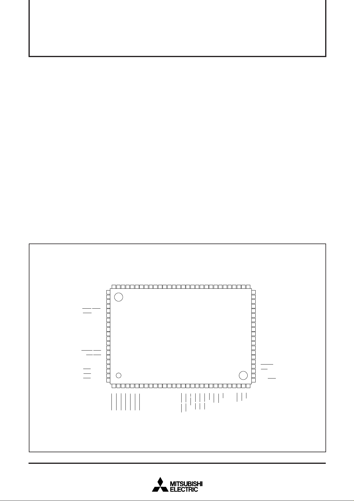
M37920S4CGP PIN CONFIGURATION (TOP VIEW)
→ A16/MA8
→ A15/MA7
→ A14/MA6
→ A13/MA5
→ A12/MA4
→ A11/MA3
→ A10/MA2
→ A9/MA1
→ A8/MA0
→ A7
→ A6
→ A5
→ A4
→ A3
→ A2
→ A1
8079787776757473727170696867666564636261605958575655545352
81
82
83
84
85
86
87
88
89
90
91
92
93
94
95
96
97
98
99
100
123456789
P66/DMAREQ3 ↔
5/TA4IN/DMAREQ2 ↔
4/TA4OUT/DMAACK2 ↔
P63/TA3IN/DMAREQ1 ↔
P6
P6
1/TA1IN/DMAREQ0 ↔
2/TA3OUT/DMAACK1 ↔
P6
P6
M37920S4CGP
101112131415161718192021222324252627282930
5/RTP11 ↔P54/RTP10 ↔P53/RTP03 ↔P52/RTP02 ↔
P5
7/TA2IN/RTP13 ↔
6/TA2OUT/RTP12 ↔
P5
P5
0/TA1OUT/DMAACK0 ↔
P6
6/WRH/UCAS ↔
1/TA0IN/RTP01 ↔
P9
0/TA0OUT/RTP00 ↔
P5
P5
6/CLK0 ↔
P8
5/RXD0 ↔
P8
P8
4/TXD0 ↔
3/CTS0/RTS0 ↔
P8
2/CTS0/CLK1 ↔
P8
1/RXD1 ↔
P8
P80/TXD1 ↔
AV
AV
3/AN3/ADTRG/INT4 ↔
P7
2/AN2/INT3 ↔
P7
1/AN1 ↔
P7
0/AN0 ↔
P7
2/INT2/TB2IN ↔
P12
1/INT1/TB1IN ↔
P12
0/INT0/TB0IN ↔
P12
V
REF
V
V
A0 ←
CC
CC
SS
SS
SS
↔ D0
← MD1
V
→ A23
→ A22/MA11
→ A21
→ A20/MA10
→ A19
→ A18/MA9
→ A17
0 ↔
CS
4/CAS/W ↔
P9
3/CS3/RAS3 ↔P92/CS2/RAS2 ↔P91/CS1/RAS1 ↔
5/WRL/LCAS ↔
P9
P9
1/φ1 ↔
2/TC ↔
P4
P4
4/HLDA ↔
3/HOLD ↔
P4
P4
↔ D4
↔ D3
↔ D2
↔ D1
51
50
↔ D5
49
↔ D6
48
↔ D7
47
↔ P20/D8
46
↔ P21/D9
45
↔ P22/D10
44
↔ P23/D11
43
↔ P24/D12
42
↔ P25/D13
41
↔ P26/D14
40
↔ P27/D15
39
VCC
38
→ XOUT
← XIN
37
SS
36
V
← MD0
35
← RESET
34
← NMI
33
← BYTE
32
↔ P30/RDY
31
RD ←
BLW ←
0/ALE ↔
3/BHW ←
P4
P3
Outline 100P6S-A
PRELIMINARY
Data bank Register DT (8)
Program Counter PC (16)
Incrementer/Decrementer (24)
Program Bank Register PG (8)
Input Buffer Register IB (16)
Direct Page Register DPR0 (16)
Stack Pointer S (16)
Index Register Y (16)
Index Register X (16)
Arithmetic Logic
Unit (16)
Accumulator B (16)
Accumulator A (16)
Instruction register (8)
Central Processing Unit
(CPU)
Incrementer (24)
Program Address Register PA (24)
Data Address Register DA (24)
Bus
Interface
Unit
(BIU)
RESET
MD1
Reference
voltage input
V
REF
(0 V)
AV
SS
AVcc
Vcc
External data bus width
select input
BYTE
Clock Generating Circuit
Clock input
X
IN
X
OUT
Data Buffer DQ0 (8)
Instruction Queue Buffer Q0 (8)
Data Bus (Odd)
Address Bus
A-D converter (10)
Watchdog timer
Timer TB1 (16)
Timer TB2 (16)
Timer TB0 (16)
Timer TA1 (16)
Timer TA2 (16)
Timer TA3 (16)
Timer TA4 (16)
Timer TA0 (16)
Input/Output
port P8
Input/Output
port P7
Input/Output
port P4
Input/Output
port P6
Input/Output
port P5
Data busInput/Output
port P2
Input/Output
port P3
MD0
(0 V)
Vss
Processor Status Register PS (11)
NMI
Data Bus (Even)
Data Buffer DQ
1
(8)
Data Buffer DQ
2
(8)
Data Buffer DQ
3
(8)
Instruction Queue Buffer Q
1
(8)
Instruction Queue Buffer Q
2
(8)
Instruction Queue Buffer Q
3
(8)
Instruction Queue Buffer Q
4
(8)
Instruction Queue Buffer Q
5
(8)
Instruction Queue Buffer Q
6
(8)
Instruction Queue Buffer Q
7
(8)
Instruction Queue Buffer Q
8
(8)
Instruction Queue Buffer Q
9
(8)
Direct Page Register DPR1 (16)
Direct Page Register DPR2 (16)
Direct Page Register DPR3 (16)
Clock output
Reset input
UART1(9)
UART0(9)
RAM
2048 bytes
P8(7)
P7(4)
P9(7)
P4(5)
P6(7)
P5(8)
DRAM controoler
DMA0(16)
DMA1(16)
DMA2(16)
DMA3(16)
P12(3)
Data I/O circuit
P2(8)P3(2)
Input/Output
port P9
Input/Output
port P12
RD
Read output
BLW
Write output
(0 V)
(5 V)
Address output circuit
Address bus
Notice: This is not a final specification.
Some parametric limits are subject to change.
MITSUBISHI MICROCOMPUTERS
M37920S4CGP
16-BIT CMOS MICROCOMPUTER
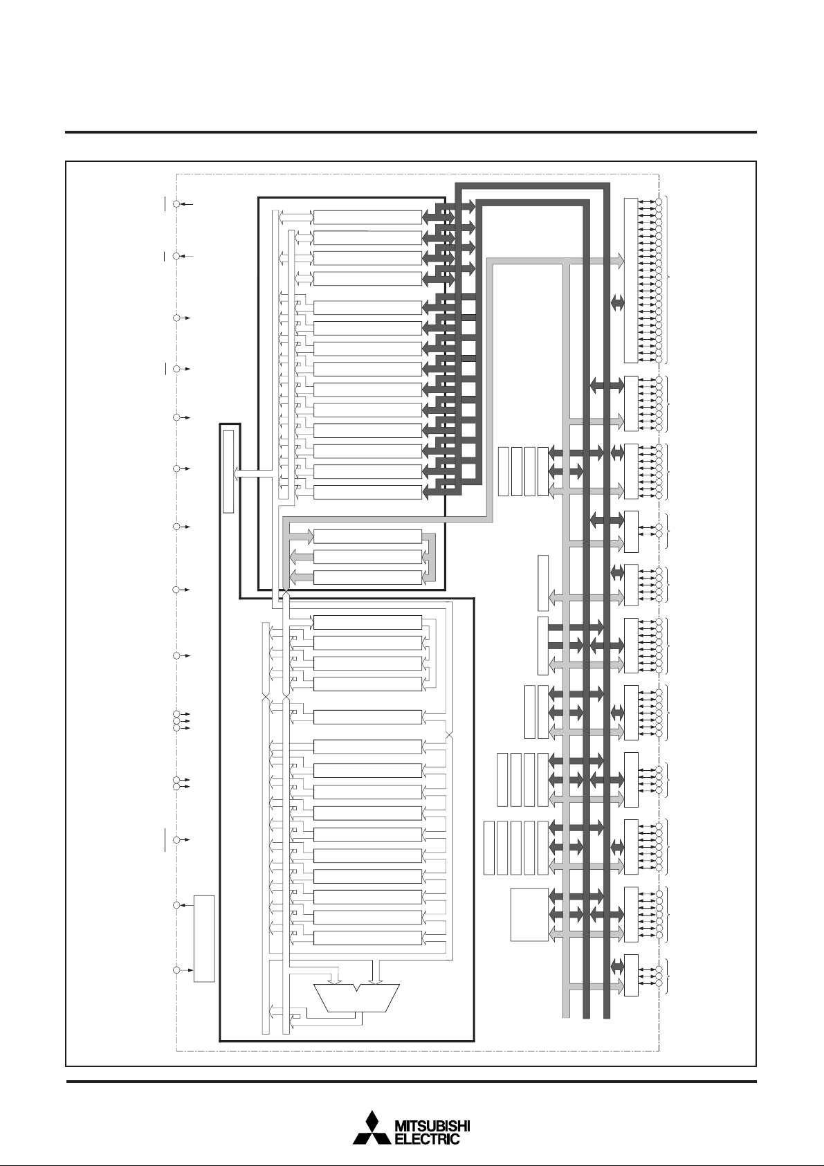
BLOCK DIAGRAM
2

PRELIMINARY
Notice: This is not a final specification.
Some parametric limits are subject to change.
FUNCTIONS (Microcomputer mode)
Number of basic machine instructions
Instruction execution time
External clock input frequency f(XIN)
Memory size
Programmable input/output
ports
Multi-functional timers
Serial I/O
A-D converter
Watchdog timer
DMA controller
DRAM controller
Chip-select wait control
ROM
RAM
P2, P5
P3
P4
P6, P8
P7
P9
P12
TA0–TA4
TB0–TB2
UART0 and UART1
MITSUBISHI MICROCOMPUTERS
M37920S4CGP
16-BIT CMOS MICROCOMPUTER
FunctionsParameter
203
50 ns (the fastest instruction at f(XIN) = 20 MHz)
20 MHz (Max.)
External
2048 bytes
8-bit ✕ 2
2-bit ✕ 1
5-bit ✕ 1
7-bit ✕ 2
4-bit ✕ 1
6-bit ✕ 1
3-bit ✕ 1
16-bit ✕ 5
16-bit ✕ 3
(UART or Clock synchronous serial I/O) ✕ 2
10-bit successive approximation method ✕ 1 (4 channels)
12-bit ✕ 1
4 channels
Maximum transfer rate 20 Mbytes/sec.
(at f(XIN) = 20 MHz, 0 wait, 1-bus cycle transfer)
10 Mbytes/sec.
(at f(XIN) = 20 MHz, 0 wait, 2-bus cycles transfer)
1 channel
Supports fast page access mode.
Incorporates 8-bit refresh timer.
Supports CAS before RAS refresh method or self refresh method.
Chip select area ✕ 4 (CS0–CS3). A wait number and bus width
can be set for each chip select area.
Real-time output
Interrupts
Clock generating circuit
Power supply voltage
Power dissipation
Ports’ input/output
characteristics
Memory expansion
Operating temperature range
Device structure
Package
Input/Output withstand voltage
Output current
4 bits ✕ 2 channels; or 6 bits ✕ 1 channel + 2 bits ✕ 1 channel
6 external types, 17 internal types. Each interrupt except NMI
can be set to a priority level within the range of 0–7 by software.
Built-in (externally connected to a ceramic resonator or quartz
crystal resonator).
5 V±10 %
135 mW (at f(XIN) = 20 MHz, typ.)
5 V
5 mA
Up to 16 Mbytes. Note that bank FF16 is a reserved area.
–20 to 85 °C
CMOS high-performance silicon gate process
100-pin plastic molded QFP
3

PRELIMINARY
Notice: This is not a final specification.
Some parametric limits are subject to change.
PIN DESCRIPTION (Microcomputer mode)
Input/
Output
—
Input
Input
Input
Input
Output
Input
—
Input
Output
Output
Output
I/O
I/O
Input
Output
Output
Output
Output
Output
I/O
Input
Output
I/O
I/O
Apply 5 V±10 % to Vcc, and 0 V to Vss.
This pin controls the processor mode. Connect this pin to VCC.
Connect this pin to Vss.
The microcomputer is reset when “L” level is applies to this pin.
These are input and output pins of the internal clock generating circuit. Connect a
ceramic or quartz- crystal resonator between the XIN and XOUT pins. When an
external clock is used, the clock source should be connected to the XIN pin, and the
XOUT pin should be left open.
This pin determines whether the external data bus has an 8-bit width or 16-bit width
for the memory expansion mode or microprocessor mode. The width is 16 bits when
“L” signal is input, and 8 bits when “H” signal is input.
Power supply input pin for the A-D converter. Connect AVcc to Vcc, and AVss to Vss
externally .
This is the reference voltage input pin for the A-D converter.
The low-order 8 bits of address (A0–A7) are output.
The middle-order 8 bits of address (A8–A15) are input/output. While DRAM space is
accessed, multiplexed address (MA0–MA7) is output.
The high-order 8 bits of address (A16–A23) are output. While DRAM space is ac-
cessed, multiplexed address (MA8–MA11) is output.
The low-order 8 bits of data (D0–D7) are input/output.
■ When 8-bit external data bus is used (BYTE = “H” level)
Port P2 is an 8-bit I/O port.
■ When 16-bit external data bus is used (BYTE = “L” level)
The high-order 8 bits (D8–D15) are input/output.
While the input level at pin RDY is “L”, the microcomputer is placed in the ready
state. While pin RD is at “L” level, the microcomputer reads out data and instruction codes. Also, pin RDY can function as a programmable I/O port pin (P30) by
software.
■ When 8-bit external data bus is used (BYTE = “H” level)
While pin BLW is at “L” level, the microcomputer writes data.
■ When 16-bit external data bus is used (BYTE = “L” level)
While pin BLW is at “L” level, the microcomputer writes data into an evennumbered address.
While pin BHW is at “L” level, the microcomputer writes data into an oddnumbered address.
Signal ALE is used to latch an address. φ1 has the same period as internal clock φ.
Pin P42 functions as a programmable I/O port pin.
While the input level at pin HOLD is at “L” level, the microcomputer is placed in the
hold state. Signal HLDA is used to inform the external that the microcomputer
enters the hold state. By software, pin ALE, clock φ1 output pin, and pins HOLD,
HLDA function as programmable I/O port pins (P40, P41, P43, P44). Pin P42 also
functions as pin TC.
Port P5 is an 8-bit I/O port. These pins also function as I/O pins for timers A0, A2,
and pulse output pins for the real-time output.
Port P6 is a 7-bit I/O port. These pins also function as I/O pins for timers A1, A3,
A4, input pins for DMA requests, and output pins for DMA acknowledge signals.
Vcc, Vss
MD0
MD1
RESET
XIN
XOUT
BYTE
AVcc,
AVss
VREF
A0–A7
A8–A15/
MA0–MA7
A16–A23/
MA8–MA11
D0–D7
P20/D8–
P27/D15
P30/RDY,
RD,
BLW,
P33/BHW
P40/ALE,
P41/φ1,
P42/TC,
P43/HOLD,
P44/HLDA
P50–P57
P60–P66
NamePin
Power supply input
MD0
MD1
Reset input
Clock input
Clock output
External data bus width
select input
Analog power supply input
Reference voltage input
Low-order address
Middle-order address/
DRAM address
High-order address/
DRAM address
Low-order data
I/O port P2/
High-order data
Memory control signal I/O
I/O port P4
I/O port P5
I/O port P6
MITSUBISHI MICROCOMPUTERS
M37920S4CGP
16-BIT CMOS MICROCOMPUTER
Functions
4

PRELIMINARY
Notice: This is not a final specification.
Some parametric limits are subject to change.
MITSUBISHI MICROCOMPUTERS
M37920S4CGP
16-BIT CMOS MICROCOMPUTER
P70–P73
P80–P86
CS0
P91–P96
P120–P122
NMI
NamePin
I/O port P7
I/O port P8
Chip-select output
I/O port P9
I/O port P12
Non-maskable interrupt
Input/
Output
I/O
I/O
Output
I/O
I/O
Input
Functions
Port P7 is a 4-bit I/O port. P72 and P73 also function as input pins for INT3 and
INT4. According to the software setting, these pins also function as input pins for
the A-D converter.
Port P8 is a 7-bit I/O port. These pins also function as I/O pins for UART0, UART1.
This is an output pin for CS0.
Port P9 is a 6-bit I/O port. According to the software setting, P91–P93 also funtion
as chip select output pins. While DRAM space is selected, P94–P96 function as
output pins for DRAM control signals.
Port P12 is a 3-bit I/O port. These pins also functions as input pins for INT0, INT1,
INT2. According to software setting, these pins also function as input pins for timers
B0–B2.
This pin is for a non-maskable interrupt.
5
PRELIMINARY
Notice: This is not a final specification.
Some parametric limits are subject to change.
MITSUBISHI MICROCOMPUTERS
M37920S4CGP
16-BIT CMOS MICROCOMPUTER
BASIC FUNCTION BLOCKS
The M37920S4CGP is the same functions as the M37920F8CGP
except for the following.
Therefore, refer to the datasheet of the M37920F8CGP.
• The M37920S4CGP does not include the internal flash memory.
• The M37920S4CGP operates only in the microprocessor mode.
• The M37920S4CGP does not have the flash memory control register (address 9E16).
• Some of programmable I/O ports of the M37920S4CGP differ from
those of the M37920FGCGP.
Bank 016
Bank 116
•
•
•
•
•
•
•
•
•
•
•
•
•
•
•
•
•
•
•
•
•
•
•
•
•
•
•
•
•
•
•
Bank FE16
Bank FF
00000016
00FFFF16
01000016
01FFFF16
FE000016
FEFFFF16
FF000016
16
FFFFFF16
00000016
0000FF16
00080016
000FFF16
00100016
00FFC016
00FFFF16
MEMORY
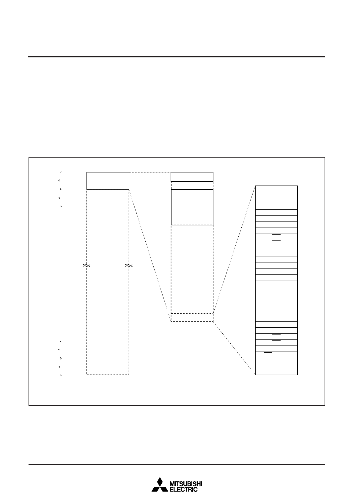
Figure 1 shows the memory map.
Peripheral devices
control registers
00FFC016
Internal RAM
2048 bytes
00FFFE16
Interrupt vector table
DMA3
DMA2
DMA1
DMA0
Address matching detect
Reserved area (Note 1)
Reserved area (Note 1)
Reserved area (Note 1)
INT4
INT3
A-D conversion
UART1 transmit
UART1 receive
UART0 transmit
UART0 receive
Timer B2
Timer B1
Timer B0
Timer A4
Timer A3
Timer A2
Timer A1
Timer A0
INT2
INT1
INT0
NMI
Watchdog timer
DBC (Note 2)
BRK instruction (Note 2)
Zero divide
RESET
Fig. 1 Memory map
6
Notes 1: Do not write to this address.
2: These are interrupts used only for debugging. Do not use these interrupts.
PRELIMINARY
Notice: This is not a final specification.
Some parametric limits are subject to change.
MITSUBISHI MICROCOMPUTERS
M37920S4CGP
16-BIT CMOS MICROCOMPUTER
Address (Hexadecimal notation)
00000016
00000116
00000216
00000316
00000416
00000516
00000616
00000716
00000816
00000916
00000A16
00000B16
00000C16
00000D16
00000E16
00000F16
00001016
00001116
00001216
00001316
00001416
00001516
00001616
00001716
00001816
00001916
00001A16
00001B16
00001C16
00001D16
00001E16
00001F16
00002016
00002116
00002216
00002316
00002416
00002516
00002616
00002716
00002816
00002916
00002A16
00002B16
00002C16
00002D16
00002E16
00002F16
00003016
00003116
00003216
00003316
00003416
00003516
00003616
00003716
00003816
00003916
00003A16
00003B16
00003C16
00003D16
00003E16
00003F16
Reserved area (Note 1)
Reserved area (Note 1)
[Port P0 register] (Note 2)
[Port P1 register] (Note 2)
[Port P0 direction register] (Note 2)
[Port P1 direction register] (Note 2)
Port P2 register
Port P3 register
Port P2 direction register
Port P3 direction register
Port P4 register
Port P5 register
Port P4 direction register
Port P5 direction register
Port P6 register
Port P7 register
Port P6 direction register
Port P7 direction register
Port P8 register
Port P9 register
Port P8 direction register
Port P9 direction register
[Port P10 register] (Note 2)
[Port P11 register] (Note 2)
[Port P10 direction register] (Note 2)
[Port P11 direction register] (Note 2)
Port P12 register
Port P12 direction register
A-D control register 0
A-D control register 1
A-D register 0
A-D register 1
A-D register 2
A-D register 3
UART0 transmit/receive mode register
UART0 baud rate register (BRG0)
UART0 transmit buffer register
UART0 transmit/receive control register 0
UART0 transmit/receive control register 1
UART0 receive buffer register
UART1 transmit/receive mode register
UART1 baud rate register (BRG1)
UART1 transmit buffer register
UART1 transmit/receive control register 0
UART1 transmit/receive control register 1
UART1 receive buffer register
Address (Hexadecimal notation)
Count start register
16
000040
00004116
00004216
00004316
00004416
00004516
00004616
00004716
00004816
00004916
00004A16
00004B16
00004C16
00004D16
00004E16
00004F16
00005016
00005116
00005216
00005316
00005416
00005516
00005616
00005716
00005816
00005916
00005A16
00005B16
00005C16
00005D16
00005E16
00005F16
00006016
00006116
00006216
00006316
00006416
00006516
00006616
00006716
00006816
00006916
00006A16
00006B16
00006C16
00006D16
00006E16
00006F16
00007016
00007116
00007216
00007316
00007416
00007516
00007616
00007716
00007816
00007916
00007A16
00007B16
00007C16
00007D16
00007E16
00007F16
One-shot start register
Up-down register
Timer A clock division select register
Timer A0 register
Timer A1 register
Timer A2 register
Timer A3 register
Timer A4 register
Timer B0 register
Timer B1 register
Timer B2 register
Timer A0 mode register
Timer A1 mode register
Timer A2 mode register
Timer A3 mode register
Timer A4 mode register
Timer B0 mode register
Timer B1 mode register
Timer B2 mode register
Processor mode register 0
Processor mode register 1
Watchdog timer register
Watchdog timer frequency select register
Particular function select register 0
Particular function select register 1
Particular function select register 2
Reserved area (Note 1)
Debug control register 0
Debug control register 1
Address comparison register 0
Address comparison register 1
3 interrupt control register
INT
4 interrupt control register
INT
A-D conversion interrupt control register
UART0 transmit interrupt control register
UART0 receive interrupt control register
UART1 transmit interrupt control register
UART1 receive interrupt control register
Timer A0 interrupt control register
Timer A1 interrupt control register
Timer A2 interrupt control register
Timer A3 interrupt control register
Timer A4 interrupt control register
Timer B0 interrupt control register
Timer B1 interrupt control register
Timer B2 interrupt control register
INT
0 interrupt control register
1 interrupt control register
INT
INT
2 interrupt control register
Notes 1: Do not read/write to this address.
2: These registers are used in the bus fixation of the power saving function. For details, refer to the
section on the power saving function of the M37920F8CGP datasheet.
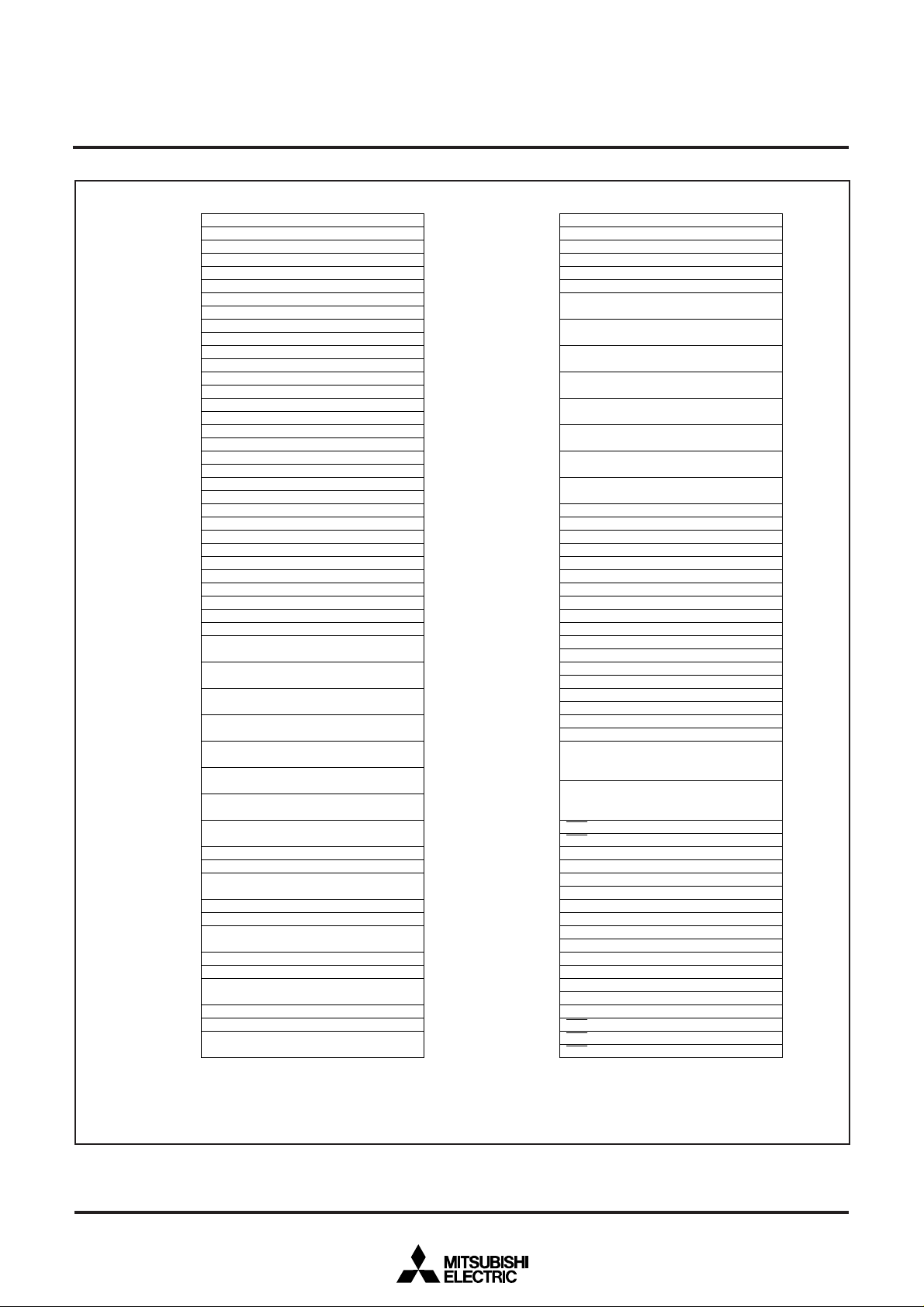
Fig. 2 Location of peripheral devices’ control registers (1)
7
PRELIMINARY
Notice: This is not a final specification.
Some parametric limits are subject to change.
MITSUBISHI MICROCOMPUTERS
M37920S4CGP
16-BIT CMOS MICROCOMPUTER
Address (Hexadecimal notation)
000080
16
control register L
0
CS
00008116
00008216
00008316
00008416
00008516
00008616
00008716
00008816
00008916
00008A16
00008B16
00008C16
00008D16
00008E16
00008F16
00009016
00009116
00009216
00009316
00009416
00009516
00009616
00009716
00009816
00009916
00009A16
00009B16
00009C16
00009D16
00009E16
00009F16
0000A016
0000A116
0000A216
0000A316
0000A416
0000A516
0000A616
0000A716
0000A816
0000A916
0000AA16
0000AB16
0000AC16
0000AD16
0000AE16
0000AF16
0000B016
0000B116
0000B216
0000B316
0000B416
0000B516
0000B616
0000B716
0000B816
0000B916
0000BA16
0000BB16
0000BC16
0000BD16
0000BE16
0000BF16
control register H
CS0
control register L
CS
1
control register H
CS
1
control register L
2
CS
control register H
2
CS
control register L
CS
3
control register H
3
CS
Area
Area
Area
Area
Reserved area (Note 1)
Reserved area (Note 1)
Reserved area (Note 1)
Real-time output control register
Pulse output data register 0
Pulse output data register 1
Reserved area (Note 1)
DRAM control register
Refresh timer
CTS/RTS separate select register
DMAC control register L
DMAC control register H
DMA0 interruput control register
DMA1 interruput control register
DMA2 interruput control register
DMA3 interruput control register
Reserved area (Note 1)
Reserved area (Note 1)
Reserved area (Note 1)
Reserved area (Note 1)
start address register
CS
0
start address register
CS
1
start address register
CS2
start address register
CS3
Address (Hexadecimal notation)
0000C016
0000C116
0000C216
0000C316
0000C416
0000C516
0000C616
0000C716
0000C816
0000C916
0000CA16
0000CB16
0000CC16
0000CD16
0000CE16
0000CF16
0000D016
0000D116
0000D216
0000D316
0000D416
0000D516
0000D616
0000D716
0000D816
0000D916
0000DA16
0000DB16
0000DC16
0000DD16
0000DE16
0000DF16
0000E016
0000E116
0000E216
0000E316
0000E416
0000E516
0000E616
0000E716
0000E816
0000E916
0000EA16
0000EB16
0000EC16
0000ED16
0000EE16
0000EF16
0000F016
0000F116
0000F216
0000F316
0000F416
0000F516
0000F616
0000F716
0000F816
0000F916
0000FA16
0000FB16
0000FC16
0000FD16
0000FE16
0000FF16
Source address
Source address
Source address
Destination address
Destination address
Destination address
Transfer counter
Transfer counter
Transfer counter
DMA0 mode
DMA0 mode
DMA0 control
Source address
Source address
Source address
Destination address
Destination address
Destination address
Transfer counter
Transfer counter
Transfer counter
DMA1 mode
DMA1 mode
DMA1 control
Source address
Source address
Source address
Destination address
Destination address
Destination address
Transfer counter
Transfer counter
Transfer counter
DMA2 mode
DMA2 mode
DMA2 control
Source address
Source address
Source address
Destination address
Destination address
Destination address
Transfer counter
Transfer counter
Transfer counter
DMA3 mode
DMA3 mode
DMA3 control
register 0 L
register 0 M
register 0 H
register 0 L
register 0 M
register 0 H
register L
register H
register
register 1 L
register 1 M
register 1 H
register 1 L
register 1 M
register 1 H
register L
register H
register
register 2 L
register 2 M
register 2 H
register 2 L
register 2 M
register 2 H
register L
register H
register
register 3 L
register 3 M
register 3 H
register 3 L
register 3 M
register 3 H
register L
register H
register
register 0 L
register 0 M
register 0 H
register 1 L
register 1 M
register 1 H
register 2 L
register 2 M
register 2 H
register 3 L
register 3 M
register 3 H
Note 1: Do not read/write to this address.
Fig. 3 Location of peripheral devices’ control registers (2)
8

PRELIMINARY
Notice: This is not a final specification.
Some parametric limits are subject to change.
MITSUBISHI MICROCOMPUTERS
M37920S4CGP
16-BIT CMOS MICROCOMPUTER
Processor mode
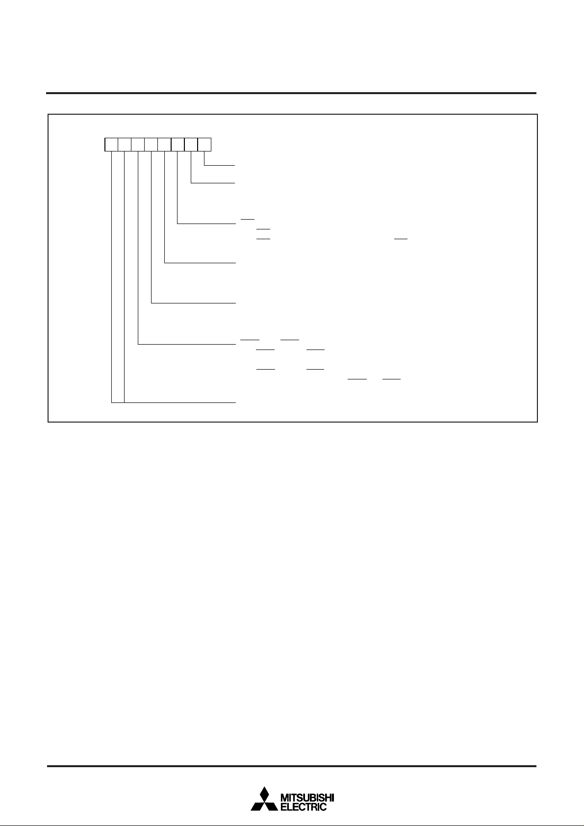
The M37920S4CGP operates only in the microprocessor mode exclusive for the external ROM. Be sure to fix the level at pin MD0 to
Vcc and the level at pin MD1 to Vss. Also, be sure to fix bits 1, 0 at
address 5E16 (the processor mode register 0) to “1” and “0”, respectively.
Microprocessor mode
When the microcomputer starts its operation after reset with the level
at pin MD0 = Vcc level (5 V), the microcomputer is placed in the microprocessor mode.
Table 1. Relationship between pins MD0, MD1 and processor mode
Pin MD0
VCC level
(5 V)
Pin MD1
VSS level
(5 V)
Processor mode
After reset, the microcomputer
starts its operation in the microprocessor mode. (Be sure
to pin MD0 to Vcc level.)
9

PRELIMINARY
Notice: This is not a final specification.
Some parametric limits are subject to change.
MITSUBISHI MICROCOMPUTERS
M37920S4CGP
16-BIT CMOS MICROCOMPUTER
76543210
Fig. 4 Processor mode register 0’s bit configuration
Processor mode register 0
Processor mode bits
0 0 : Do not select.
0 1 : Do not select.
1 0 : Microprocessor mode
1 1 : Do not select.
External bus wait number select bits
0 0 : 0 wait
0 1 : 1 wait
1 0 : 2 wait
1 1 : ALE expansion wait
Interrupt priority detection time select bits
0 0 : 7 cycles of φ
0 1 : 4 cycles of φ
1 0 : 2 cycles of φ
1 1 : Do not select.
Software reset bit
By a write of “1” to this bit, the microcomputer will be reset, and then, restarted.
1 output select bit
Clock φ
1 output is disabled. (P41 functions as a programmable I/O port pin.)
0 : φ
1 output is enabled. (P41 functions as the clock φ1 output pin.)
1 : φ
Address
5E
16
10
PRELIMINARY
Notice: This is not a final specification.
Some parametric limits are subject to change.
MITSUBISHI MICROCOMPUTERS
M37920S4CGP
16-BIT CMOS MICROCOMPUTER
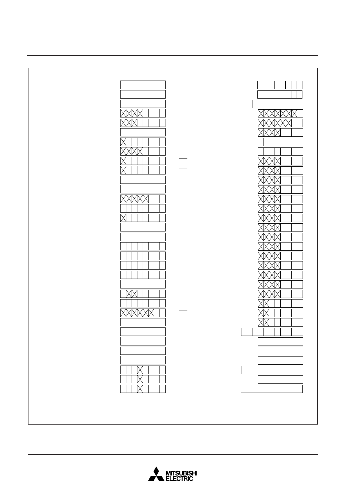
76543210
00
0
Processor mode register 1
Fix this bit to “0”.
Direct page register switch bit
0 : Only DPR0 is used.
1 : DPR0 to DPR3 are used.
RDY input select bit
0 : RDY input is disabled. (P3
1 : RDY input is enabled. (P3
ALE output select bit
0 : ALE output is disabled. (P4
1 : ALE output is enabled. (P4
Recovery cycle insert select bit
0 : No recovery cycle is inserted at access to the external area.
1 : Recovery cycle is inserted at access to the external area.
HOLD input, HLDA output select bit
0 : HOLD input and HLDA output are disabled.
1 : HOLD input and HLDA output are enabled.
“0” at read.
Address
16
5F
0 functions as a programmable I/O port pin.)
0 functions as pin RDY.)
0 functions as a programmable I/O port pin.)
0 functions as pin ALE.)
0 and P44 function as programmable I/O port pins.)
(P4
3 and P44 function as pins HOLD and HLDA, respectively.)
(P4
Fig. 5 Processor mode register 1’s bit configuration
11
PRELIMINARY
Notice: This is not a final specification.
Some parametric limits are subject to change.
MITSUBISHI MICROCOMPUTERS
M37920S4CGP
16-BIT CMOS MICROCOMPUTER
Address
(
)
16
04
Port P0 direction register 00
UART 0 Transmit/Receive mode register
UART 1 Transmit/Receive mode register
UART 0 Transmit/Receive control register 0
UART 1 Transmit/Receive control register 0
UART 0 Transmit/Receive control register 1
UART 1 Transmit/Receive control register 1
Timer A clock division select register
···
(
)
05
···Port P1 direction register
16
(
)
08
···Port P2 direction register
16
(
)
09
···Port P3 direction register
16
(
)
16
0C
···Port P4 direction register
(
)
16
0D
···Port P5 direction register 00
(
)
16
10
···Port P6 direction register
(
)
11
16
···Port P7 direction register
(
)
14
16
···Port P8 direction register
(
)
15
16
···Port P9 direction register
(
)
18
···Port P10 direction register 00
16
(
)
19
···Port P11 direction register 00
16
(
)
1C
···Port P12 direction register
16
)
(
···A-D control register 0
1E
16
)
(
···A-D control register 1
1F
16
(
)
16
30
···
(
)
38
···
16
)
(
16
···
34
(
)
3C
16
···
)
(
···
16
35
)
(
···
16
3D
(
)
16
40
···Count start register 00
)
(
···One-shot start register
16
42
)
(
16
···Up-down register
44
)
(
16
···
45
(
)
56
16
···Timer A0 mode register 00
(
)
57
···Timer A1 mode register 00
16
(
)
58
···Timer A2 mode register 00
16
(
)
59
···Timer A3 mode register 00
16
(
)
16
5A
···Timer A4 mode register 00
)
(
16
···Timer B0 mode register
5B
)
(
16
···Timer B1 mode register
5C
(
)
5D
···Timer B2 mode register
16
00
00
00
0
16
16
00
16
0000
00 000
16
0000 000
0000
0000 000
0000 000
16
16
000
00000 ???
0000 001
00
16
00
16
100 000
100 000
00000 010
00000 010
16
00 000
00000
000
16
16
16
16
16
00?0 000
00?0 000
00?0 000
00
Address
(
5E
(
5F
(
60
Watchdog timer
Watchdog timer frequency select register
Particular function select register 0
Particular function select register 1
3
interrupt control register
4
interrupt control register
A-D conversion interrupt control register
UART 0 transmit interrupt control register
UART 0 receive interrupt control register
UART 1 transmit interrupt control register
UART 1 receive interrupt control register
0
interrupt control register
1
interrupt control register
INT
2
interrupt control register
16
(
61
(
62
(
63
(
66
(
67
(
6E
(
6F
(
70
(
71
(
72
(
73
(
74
(
75
(
76
(
77
(
78
(
79
(
7A
(
7B
(
7C
(
7D
(
7E
(
7F
Processor status register PS
Program bank register PG
Program counter PC
Program counter PC
H
L
Direct page registers DPR0 to DPR3
Data bank register DT
Stack pointer
)
16
···Processor mode register 0
(Note 2)
)
16
···Processor mode register 1
)
···
)
···
16
)
···
16
)
···
16
)
16
···Debug control register 0
)
16
···Debug control register 1
)
16
···INT
)
16
···INT
)
16
···
)
16
···
)
16
···
)
16
···
)
16
···
)
16
···Timer A0 interrupt control register
)
16
···Timer A1 interrupt control register
)
···Timer A2 interrupt control register
16
)
···Timer A3 interrupt control register
16
)
16
···Timer A4 interrupt control register
)
16
···Timer B0 interrupt control register
)
16
···Timer B1 interrupt control register
)
16
···Timer B2 interrupt control register
)
16
···INT
)
···INT
16
)
16
···
(Note 2)
0000
FFF
(Note 3)
(Note 3)
010 0 000
000
Contents at address FFFF
Contents at address FFFE
0000
16
FFF
16
1000
0
16
00
0000
0000
?000
0000
0000
0000
0000
0000
0000
0000
0000
0000
0000
0000
0000
000 000
000 000
000
000
1??
000??
00
16
00
16
(Note 2)
00
(Note 3)
(Note 3)
16
16
0
0
Notes 1: The contents of the other registers and RAM are undefined at reset and must be initialized by software.
2: The status just after reset depends on the voltage level applied to pin MD0.
3: At power-on reset, these bits are clear to “0”. At hardware or software reset, on the other hand, these bits retain the state just before reset.
Fig. 6 Microcomputer internal status just after reset (1)
12
 Loading...