


MITSUBISHI MICROCOMPUTERS
M37905F8CFP, M37905F8CSP
PRELIMINARY
Notice: This is not a final specification.
Som
etric limits are subject to change.
e param
DESCRIPTION
These are single-chip 16-bit microcomputers designed with high-performance CMOS silicon gate technology, including the internal flash
memory and, being packaged in 64-pin plastic molded QFP or shrink
plastic molded DIP. These microcomputers support the 7900 Series
instruction set, which are enhanced and expanded instruction set
and are upper-compatible with the 7700/7751 Series instruction set.
The CPU of these microcomputers is a 16-bit parallel processor that
can also be switched to perform 8-bit parallel processing. Also, the
bus interface unit of these microcomputers enhances the memory
access efficiency to execute instructions fast. Therefore, these microcomputers are suitable for office, business, and industrial equipment controller that require high-speed processing of large data.
Also, they are suitable for motor-control equipment since each of
them includes the motor control circuit.
For the internal flash memory, single-power-supply programming
and erasure, using a PROM programmer or the control by the central processing unit (CPU), is supported. Also, each of these microcomputers has the memory area dedicated for storing a certain
software which controls programming and erasure (reprogramming
control software). Therefore, on these microcomputers, the program
can easily be changed even after they are mounted on the board.
16-BIT CMOS MICROCOMPUTER
<Flash memory mode>
Power supply voltage .................................................. 5 V ± 0.5 V
•
Programming/Erase voltage........................................ 5 V ± 0.5 V
•
Programming method.................... Programming in a unit of word
•
Erase method ............................................
•
M37905F8CFP, M37905F8CSP
............... 4 blocks (8 Kbytes ✕ 2, 16 Kbytes ✕ 1, 28 Kbytes ✕ 1)
Programming/Erase control by software command
•
Maximum number of reprograms ............................................ 100
•
Block erase or Total erase
APPLICATION
Control devices for office equipment such as copiers and facsimiles
•
Control devices for industrial equipment such as communication
•
and measuring instruments
Control devices for equipment, requiring motor control, such as
•
inverter air conditioners and general-purpose inverters
DISTINCTIVE FEATURES
<Microcomputer mode>
Number of basic machine instructions .................................... 203
•
Memory
•
Flash memory (User ROM area) ................................... 60 Kbytes
RAM .............................................................................3072 bytes
Flash memory (Boot ROM area) ..................................... 8 Kbytes
Instruction execution time
•
The fastest instruction at 20 MHz frequency ........................ 50 ns
Single power supply .................................................... 5 V ± 0.5 V
•
Interrupts ........... 8 external sources, 23 internal sources, 7 levels
•
Multi-functional 16-bit timer ................................................. 10 + 3
•
(Three-phase motor drive waveform or Pulse motor drive waveform
output is available.)
Serial I/O (UART or Clock synchronous)..................................... 3
•
10-bit A-D converter ..........................................12-channel inputs
•
8-bit D-A converter ............................................2-channel outputs
•
12-bit watchdog timer
•
Programmable input/output (ports P1, P2, P4, P5, P6, P7, P8)......
•
50
MITSUBISHI MICROCOMPUTERS
M37905F8CFP, M37905F8CSP
PRELIMINARY
Notice: This is not a final specification.
e param
Som
its are subject to change.
etric lim
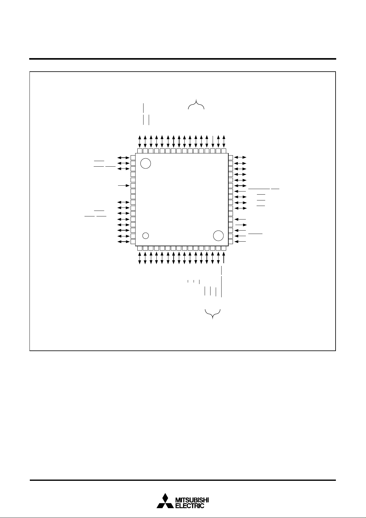
M37905F8CFP PIN CONFIGURATION (TOP VIEW)
1
1
/CLK
/RTS
1
1
1
OUT
1
/TA4
/TxD
/RxD
/CTS
/CTS
4
P1
5
P1
6
P1
7
P1
0
P2
M37905F8CFP
P12/RXD
P11/CTS0/CLK
P10/CTS0/RTS
V
AV
V
AV
P83/AN11/TXD
V
P82/AN10/RXD
P81/AN9/CTS2/CLK
P80/AN8/CTS2/RTS2/DA
P77/AN7/DA
P76/AN
P75/AN
P74/AN
CC
CC
REF
SS
SS
0
/TxD
3
P1
48474645444342414039383736
0
49
50
0
51
0
52
53
54
55
56
2
57
2
58
2
59
1
60
0
61
6
62
5
63
4
64
123456789
IN
/TA4
1
P2
OUT
/TA9
2
P2
IN
/TA9
3
P2
)
IN
(/TB2
6
P27P2
MD1
35
0
/RTP2
OUT
/TA5
0
P4
34
Note
)
)
IN
IN
(/TB1
(/TB0
5
4
P2
P2
10111213141516
1
/RTP2
IN
/TA5
1
P4
33
32
31
30
29
28
27
26
25
24
23
22
21
20
19
18
17
16-BIT CMOS MICROCOMPUTER
P42/TA6
OUT
/RTP2
P43/TA6IN/RTP2
P44/TA7
OUT
P45/TA7IN/RTP3
P46/TA8
OUT
P47/TA8IN/RTP3
P4OUT
CUT
P51/INT
1
P52/INT2/RTP
P53/INT3/RTP
V
SS
V
CONT
X
OUT
IN
X
RESET
MD0
/RTP3
/RTP3
/INT
2
3
0
1
2
3
0
TRG1
TRG0
1
/AN
1
P7
0
/AN
0
P7
2
3
/RTP1
/RTP1
IN
OUT
/TA3
7
/TA3
6
P6
P6
3
/AN
3
P7
2
/AN
2
P7
Outline 64P6N-A
3
0
1
/V/RTP1
/U/RTP1
/W/RTP0
IN
IN
OUT
/TA2
/TA1
5
3
/TA2
4
P6
P6
P6
0
1
2
/V/RTP0
/U/RTP0
/W/RTP0
IN
OUT
OUT
/TA0
1
/TA1
/TA0
2
0
P6
P6
P6
/IDU
IN
/TB2
7
/INT
7
P5
4
/IDV
/IDW
/INT
IN
IN
CUT
/TB1
/TB0
6
5
/INT
P6OUT
/INT
6
5
P5
P5
Note
Note: Allocation of pins TB0IN to TB2IN
can be switched by software.
2
MITSUBISHI MICROCOMPUTERS
M37905F8CFP, M37905F8CSP
PRELIMINARY
Notice: This is not a final specification.
e param
Som
its are subject to change.
etric lim
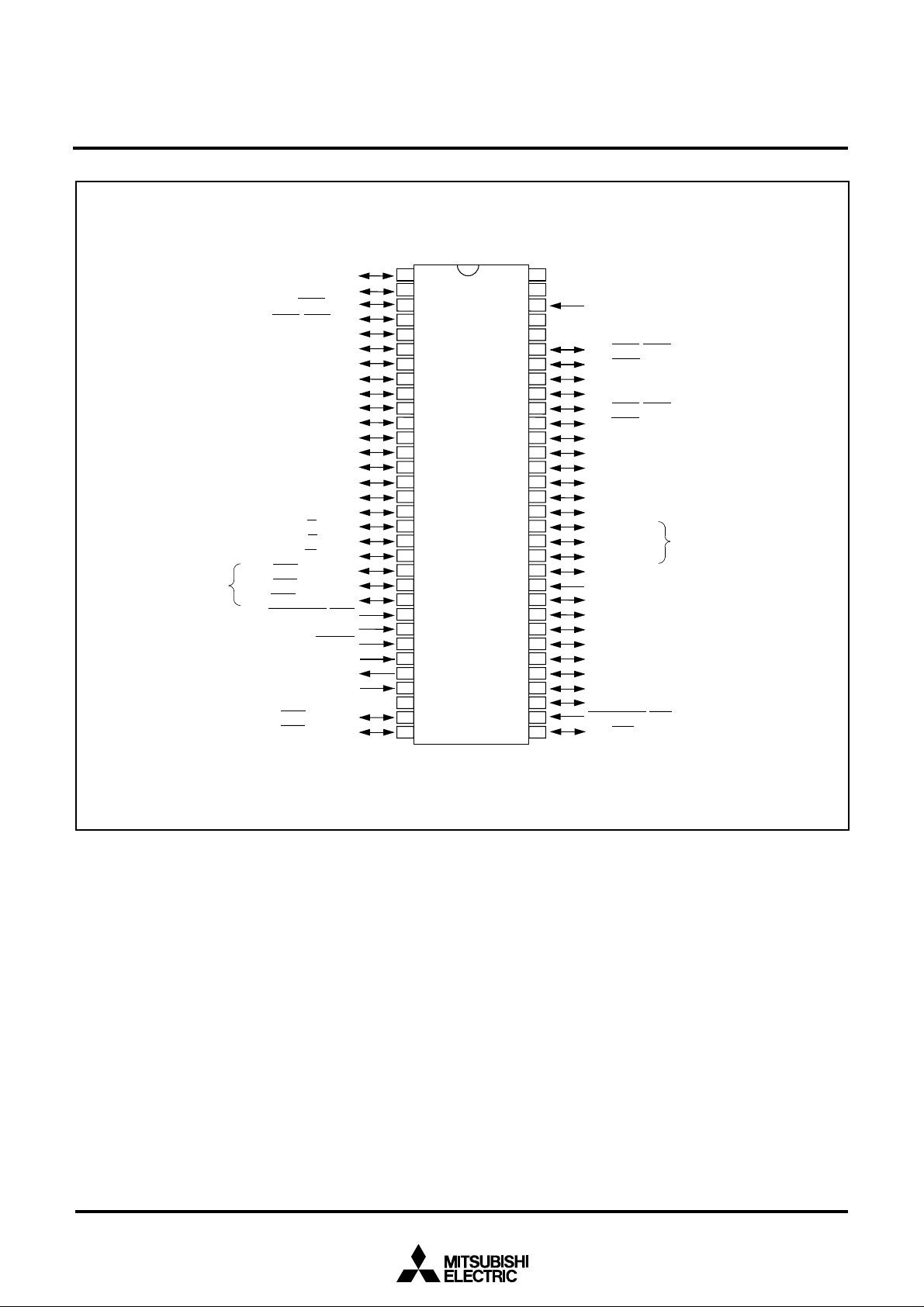
M37905F8CSP PIN CONFIGURATION (TOP VIEW)
2
/TxD
11
/AN
3
P81/AN9/CTS2/CLK
P80/AN8/
P66/TA3OUT/RTP12
P65/TA2IN/U/RTP11
P64/TA2OUT/V/RTP10
P63/TA1IN/W/RTP03
P62/TA1OUT/U/RTP02
P61/TA0IN/V/RTP01
P60/TA0OUT/W/RTP00
P57/INT7/TB2IN/IDU
Note
P5
5/INT5/TB0IN/IDW
P5
P53/INT3/RTPTRG0
P52/INT2/RTPTRG1
P8
/RxD
10
/AN
2
P8
CTS2/RTS2/
DA1
P77/AN7/DA0
P76/AN6
P75/AN5
P74/AN4
P73/AN3
P72/AN2
P71/AN1
P70/AN0
P67/TA3IN/RTP13
6/INT6/TB1IN/IDV
P6OUTCUT/INT4
MD0
RESET
XIN
XOUT
V
CONT
VSS
2
2
1
2
3
4
5
6
7
8
9
10
11
12
13
14
15
16
17
18
19
20
21
22
23
24
25
26
27
28
29
30
31
32
64
63
62
61
60
59
58
57
56
55
54
53
M37905F8CSP
52
51
50
49
48
47
46
45
44
43
42
41
40
39
38
37
36
35
34
33
16-BIT CMOS MICROCOMPUTER
SS
V
AVSS
VREF
AVCC
VCC
P10/CTS0/RTS0
P11/CTS0/CLK0
P12/RxD0
P13/TxD0
P14/CTS1/RTS1
5/CTS1/CLK1
P1
P16/RxD1
P17/TxD1
P20/TA4OUT
P21/TA4IN
P22/TA9OUT
P23/TA9IN
P24(/TB0IN)
P25(/TB1IN)
6(/TB2IN)
P2
7
P2
MD1
P40/TA5OUT/RTP20
P41/TA5IN/RTP21
P42/TA6OUT/RTP22
P43/TA6IN/RTP23
P44/TA7OUT/RTP30
P45/TA7IN/RTP31
P46/TA8OUT/RTP32
P47/TA8IN/RTP33
P4OUTCUT/INT0
P51/INT1
Note
Outline 64P4B
Note: Allocation of pins TB0IN to TB2IN
can be switched by software.
3
MITSUBISHI MICROCOMPUTERS
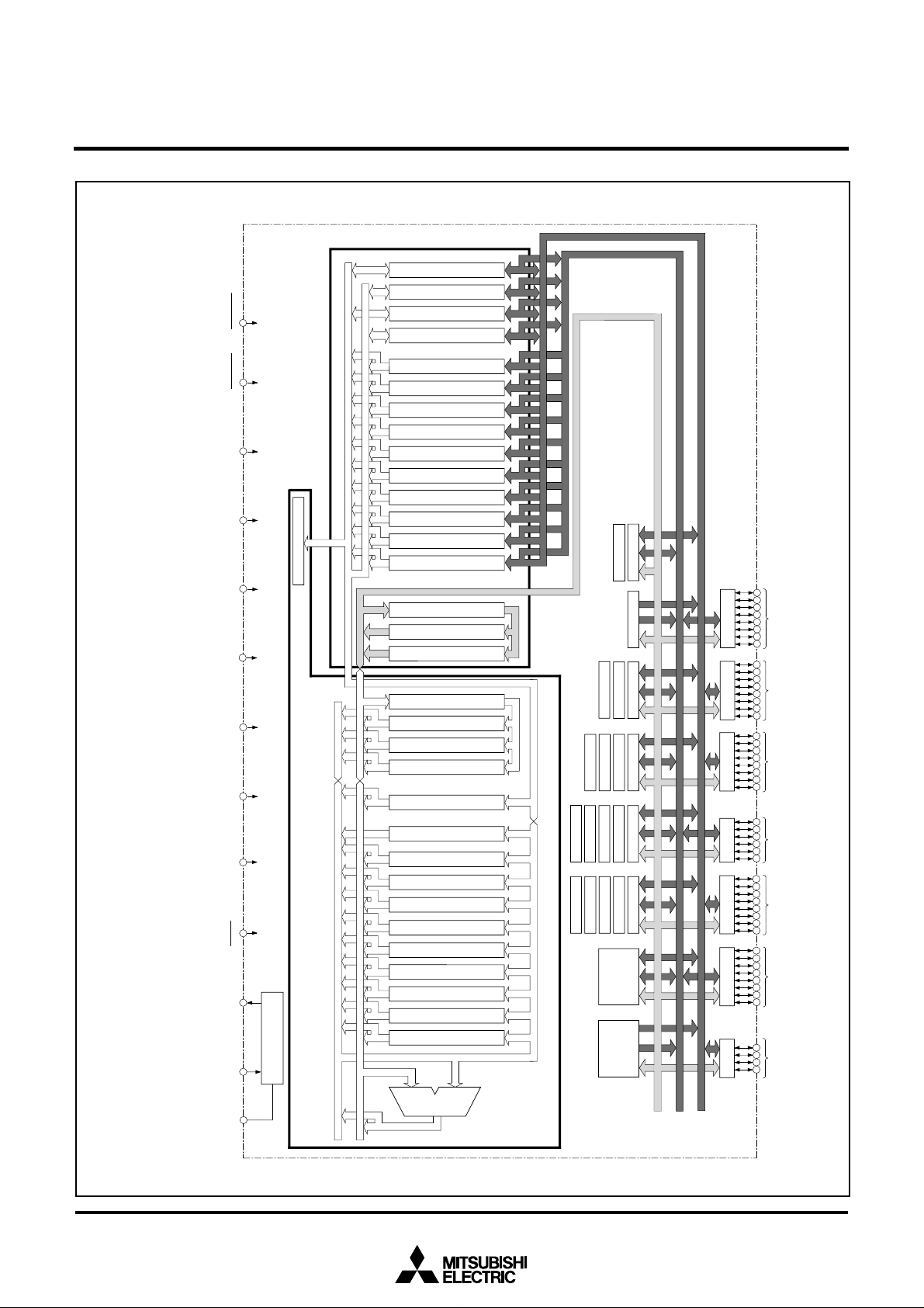
Central Processing Unit (CPU)
Bus
Interface
Unit
(BIU)
RESET
MD1
V
Reference
Voltage Input
Instruction Register (8)
REF
(0V)
AV
SS
AV
CC
V
CC
X
Clock input
Clock Generating Circuit
Reset inputClock output
IN
X
OUT
Address Bus
Data Bus (Odd)
Data Bus (Even)
A-D Converter (12)
UART1 (9)
UART0 (9)
Watchdog Timer
Timer TB1 (16)
Timer TB2 (16)
Timer TB0 (16)
D-A
1
Converter (8)
Timer TA1 (16)
Timer TA2 (16)
Timer TA3 (16)
Timer TA4 (16)
Timer TA0 (16)
RAM
3072 bytes
P6(8)
Input/Output P6
P5(6)
Input/Output P5
P7(8)
Input/Output P7
P4(8)
Input/Output P4
D-A
0
Converter (8)
P8(4)
Input/Output P8
MD0
(0V)
V
SS
P4OUT
CUT
ROM
60 Kbytes
V
CONT
Timer TA6 (16)
Timer TA7 (16)
Timer TA8 (16)
Timer TA9 (16)
Timer TA5 (16)
P6OUT
CUT
P2(8)
Input/Output P2
P1(8)
Input/Output P1
UART2 (9)
Data Buffer DQ0 (8)
Data Buffer DQ
1
(8)
Data Buffer DQ
2
(8)
Data Buffer DQ
3
(8)
Instruction Queue Buffer Q
0
(8)
Instruction Queue Buffer Q
1
(8)
Instruction Queue Buffer Q
2
(8)
Instruction Queue Buffer Q
3
(8)
Instruction Queue Buffer Q
4
(8)
Instruction Queue Buffer Q
5
(8)
Instruction Queue Buffer Q
6
(8)
Instruction Queue Buffer Q
7
(8)
Instruction Queue Buffer Q
8
(8)
Instruction Queue Buffer Q
9
(8)
Program Address Register PA (24)
Data Address Register DA (24)
Incrementer (24)
Incrementer/Decrementer (24)
Input Buffer Register IB (16)
Program Counter PC (16)
Program Bank Register PG (8)
Processor Status Register PS (11)
Direct Page Register DPR0 (16)
Direct Page Register DPR1 (16)
Direct Page Register DPR2 (16)
Direct Page Register DPR3 (16)
Stack Pointer S (16)
Index Register Y (16)
Index Register X (16)
Accumulator B (16)
Accumulator A (16)
Arithmetic Logic
Unit (16)
Data Bank Register DT (8)
M37905F8CFP, M37905F8CSP
PRELIMINARY
Notice: This is not a final specification.
e param
Som
its are subject to change.
etric lim
16-BIT CMOS MICROCOMPUTER
BLOCK DIAGRAM
4
MITSUBISHI MICROCOMPUTERS
M37905F8CFP, M37905F8CSP
PRELIMINARY
Notice: This is not a final specification.
e param
Som
its are subject to change.
etric lim
FUNCTIONS (Microcomputer mode)
Number of basic machine instructions
Instruction execution time
External clock input frequency f(X
System clock frequency f(f
Memory size
Programmable input/output
ports
Multi-functional timers
Serial I/O
A-D converter
D-A converter
Dead-time timer
Watchdog timer
Interrupts
Clock generating circuit
PLL frequency multiplier
Power supply voltage
Power dissipation
Ports’ input/output
characteristics
Memory expansion
Operating ambient temperature range
Device structure
Package
IN)
sys)
Flash memory (User ROM area)
RAM
Flash memory (Boot ROM area)
P1, P2, P4, P6, P7
P5
P8
TA0–TA9
TB0–TB2
UART0, UART1, and UART2
Maskable interrups
Non-maskable interrups
Input/Output withstand voltage
Output current
16-BIT CMOS MICROCOMPUTER
FunctionsParameter
203
50 ns (the fastest instruction at f(f
20 MHz (Max.)
20 MHz (Max.)
60 Kbytes
3072 bytes
8 Kbytes
8-bit ✕ 5
6-bit ✕ 1
4-bit ✕ 1
16-bit ✕ 10
16-bit ✕ 3
(UART or Clock synchronous serial I/O) ✕ 3
10-bit successive approximation method ✕ 1 (12 channels)
8-bit ✕ 2
8-bit ✕ 3
12-bit ✕ 1
8 external sources, 20 internal sources. Each interrupt can be set
to a priority level within the range of 0–7 by software.
3 internal sources.
Incorporated (externally connected to a ceramic resonator or
quartz crystal resonator).
The following multiplication ratios are available: ✕2, ✕3, ✕4.
5 V±0.5 V
125 mW (at f(f
is inactive.)
5 V
5 mA
Not available (single-chip mode only).
–20 to 85 °C
CMOS high-performance silicon gate process
(Note)
sys) = 20 MHz, Typ., ; the PLL frequency multiplier
sys) = 20 MHz)
Note:
Packages M37905F8CFP 64-pin plastic molded QFP (64P6N-A)
M37905F8CSP
64-pin shrink plastic moldeds DIP (64P4B)
5
MITSUBISHI MICROCOMPUTERS
M37905F8CFP, M37905F8CSP
PRELIMINARY
Notice: This is not a final specification.
e param
Som
its are subject to change.
etric lim
16-BIT CMOS MICROCOMPUTER
FUNCTIONS (Flash memory mode)
FunctionsParameter
Power supply voltage
Programming/Erase voltage
Flash memory mode
Block division for erasure
Programming method
Erase method
Programming/Erase control
Number of commands
Maximum number of reprograms
Note: On shipment, our reprogramming control firmware for the flash memory serial I/O mode has been stored into the boot ROM area.
User ROM area
Boot ROM area
Flash memory parallel I/O mode
Flash memory serial I/O mode
Flash memory CPU reprogramming mode
Flash memory parallel I/O mode
Flash memory serial I/O mode
Flash memory CPU reprogramming mode
5 V±0.5 V
5 V±0.5 V
3 modes: parallel I/O, serial I/O, and CPU reprogramming modes
4 blocks (8 Kbytes ✕ 2, 16 Kbytes ✕ 1, 28 Kbytes ✕ 1); total of
60 Kbytes
1 block (8 Kbytes ✕ 1) (Note)
Programmed per word
User ROM area + Boot ROM area
User ROM area
User ROM area
Total erase/Block erase
User ROM area + Boot ROM area
User ROM area
User ROM area
Programming/Erase control by software commands
6 commands
100
6
MITSUBISHI MICROCOMPUTERS
M37905F8CFP, M37905F8CSP
PRELIMINARY
Notice: This is not a final specification.
e param
Som
its are subject to change.
etric lim
PIN DESCRIPTION (MICROCOMPUTER MODE)
Input/
Output
—
Input
Input
Input
Input
Output
—
—
Input
I/O
I/O
I/O
I/O
I/O
I/O
I/O
Input
Input
Apply 5 V±0.5 V to Vcc, and 0 V to Vss.
Connect this pin to V
Connect this pin to Vss.
The microcomputer is reset when “L” level is applies to this pin.
These are input and output pins of the internal clock generating circuit. Connect a
ceramic resonator or quartz-crystal oscillator between pins X
external clock is used, the clock source should be connected to pin X
X
OUT should be left open.
When using the PLL frequency multiplier, connect this pin to the filter circuit. When
not using the PLL frequency multiplier, this pin should be left open.
Power supply input pins for the A-D and D-A converters. Connect AVcc to Vcc, and
AVss to Vss externally.
This is the reference voltage input pin for the A-D and D-A converters.
Port P1 is an 8-bit I/O port. This port has an I/O direction register, and each pin can
be programmed for input or output. These pins enter the input mode ar reset. These
pins also function as I/O pins of UART0, 1.
In addition to having the same functions as port P1, these pins function as I/O pins
for timers A4 and A9. Also, they can be programmed to function as input pins for timers B0 to B2.
In addition to having the same functions as port P1, these pins function as I/O pins
for timers A5 to A8. Also, they function as output pins for motor drive waveform.
In addition to having the same functions as port P1, these pins function as input pins
for INT
1 to INT3 and INT5 to INT7. Also, pins P55 to P57 function as input pins for tim-
ers B0 to B2 and as input pins for position data in the three-phase waveform mode;
and pins P5
In addition to having the same functions as port P1, these pins function as I/O pins
for timers A0 to A3. Also, they function as motor drive waveform output pins.
In addition to having the same functions as port P1, these pins function as input pins
for the A-D converter. Also, P7
In addition to having the same functions as port P1, these pins function as input pins
for the A-D converter. Also, these pins function as I/O pins for UART2, and pin P8
functions as an output pin for the D-A converter.
This pin has the function to forcibly place port P4 pins in the input mode. Also, this
pin functions as an input pin for INT
forcibly cuts off a motor drive waveform output.
This pin has the function to forcibly place port P6 pins in the input mode. Also, this
pin functions as an input pin for INT
forcibly cuts off a motor drive waveform output.
Vcc, Vss
MD0
MD1
RESET
IN
X
XOUT
VCONT
AVcc,
AVss
V
REF
P10–P17
P20–P27
P40–P47
P51–P53,
P55–P57
P60–P67
P70–P77
P80–P83
P4OUTCUT
P6OUTCUT
NamePin
Power supply input
MD0
MD1
Reset input
Clock input
Clock output
Filter circuit connection
Analog power supply input
Reference voltage input
I/O port P1
I/O port P2
I/O port P4
I/O port P5
I/O port P6
I/O port P7
I/O port P8
CUT input
P4OUT
P6OUT
CUT input
16-BIT CMOS MICROCOMPUTER
Functions
SS.
IN and XOUT. When an
IN, and pin
2 and P53 function as trigger-input pins in the pulse output port mode.
7 functions as an output pin for the D-A converter.
0
0; and this pin is used to input a signal, which
4; and this pin is used to input a signal, which
7
MITSUBISHI MICROCOMPUTERS
M37905F8CFP, M37905F8CSP
PRELIMINARY
Notice: This is not a final specification.
e param
Som
its are subject to change.
etric lim
PIN DESCRIPTION (FLASH MEMORY SERIAL I/O MODE)
Pin
VCC, VSS
MD0
MD1
_____
RESET
X
IN
XOUT
AVcc, AVss
V
REF
P10–P17
P20–P23, P2
P24
P25
P26
P4OUTCUT
P6OUTCUT
P40–P47
P55–P53,
P55–P57
P60–P67
P70–P74
P80–P83
VCONT
Name
Power supply input
MD0
MD1
Reset input
Clock input
Clock output
Analog supply input
Reference voltage input
Input port P1
Input port P2
7
SCLK input
SDA I/O
BUSY output
P4OUT
CUT input
P6OUT
CUT input
Input port P4
Input port P5
Input port P6
Input port P7
Input port P8
Filter circuit connection
Input
/Output
—
Input
Input
Input
Input
Output
—
Input
Input
Input
Input
I/O
Output
Input
Input
Input
Input
Input
Input
Input
—
Apply 5 V ± 0.5 V to Vcc, and 0 V to Vss.
Connect this pin to Vss.
Connect this pin to Vss via a resistor of 10 kΩ to 100 kΩ.
The reset input pin.
Connect a ceramic oscillator between the X
clock from the X
IN pin with the XOUT pin left open.
Connect AVcc to Vcc, and AVss to Vss.
Input an arbitrary level within the range of VSS–VCC. (This is not used in the flash memory serial I/O mode.)
Input “H” or “L”, or leave them open. (This is not used in the flash memory serial I/O mode.)
Input “H” or “L”, or leave them open. (This is not used in the flash memory serial I/O mode.)
This is an input pin for a serial clock.
This is an I/O pin for serial data. Connect this pin to V
This is an output pin for the BUSY signal.
Input “H”.
Input “H”.
Input “H” or “L”, or leave them open. (This is not used in the flash memory serial I/O mode.)
Input “H” or “L”, or leave them open. (This is not used in the flash memory serial I/O mode.)
Input “H” or “L”, or leave them open. (This is not used in the flash memory serial I/O mode.)
Input “H” or “L”, or leave them open. (This is not used in the flash memory serial I/O mode.)
Input “H” or “L”, or leave them open. (This is not used in the flash memory serial I/O mode.)
Connect this pin to the filter circuit, or leave this pin open. (This is not used in the flash
memory serial I/O mode.)
16-BIT CMOS MICROCOMPUTER
Functions
IN and XOUT pins, or input an external
CC via a resistor (about 1 kΩ).
8
MITSUBISHI MICROCOMPUTERS
M37905F8CFP, M37905F8CSP
PRELIMINARY
Notice: This is not a final specification.
e param
Som
its are subject to change.
etric lim
BASIC FUNCTION BLOCKS
Each of the M37905F8CFP and M37905F8CSP has the same function as that of the M37905M4C-XXXFP except for the following.
Therefore, for details except for the following, refer to the datasheet
of the M37905M4C-XXXFP.
• Internal ROM: type (flash memory) and size
• RAM size
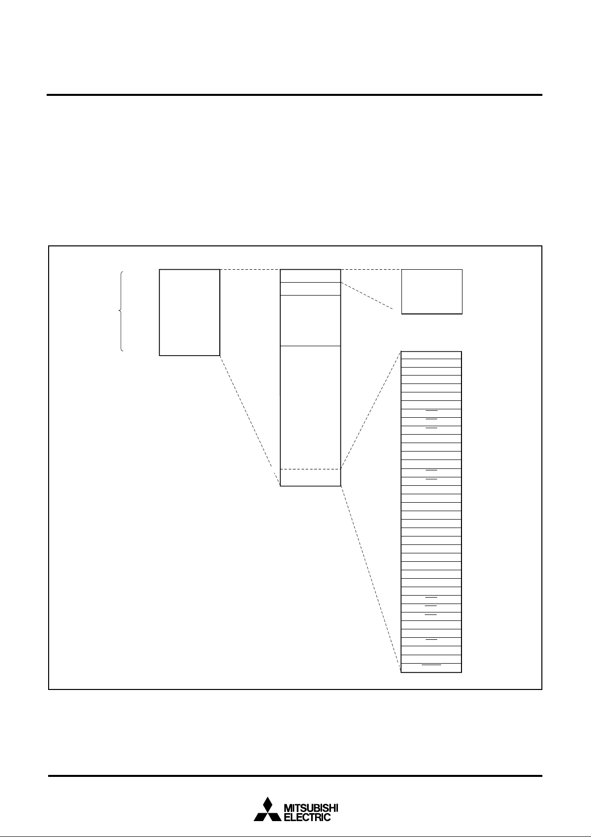
MEMORY
Figure 1 shows the memory map.
000000
Bank 0
16
16
00FFFF
16
000000
0000FF
000100
0003FF
000400
000FFF
001000
00FFB4
00FFFF
16
16
16
16
16
16
16
16
16
Peripheral devices
control registers
Unused area
Internal RAM
3072 bytes
Internal ROM
60 Kbytes
000000
0000FF
00FFB4
00FFFE
16-BIT CMOS MICROCOMPUTER
16
Peripheral devices
control registers
(See Figures 2 and 3.)
16
Interrupt vector table
16
UART2 transmit
UART2 receive
Timer A9
Timer A8
Timer A7
Timer A6
Timer A5
INT
7
INT
6
INT
5
Reserved area
Address matching detect
Reserved area
Reserved area
INT
4
INT
3
A-D conversion
UART1 transmit
UART1 receive
UART0 transmit
UART0 receive
Timer B2
Timer B1
Timer B0
Timer A4
Timer A3
Timer A2
Timer A1
Timer A0
INT
2
INT
1
INT
0
Reserved area
Watchdog timer
DBC
BRK instruction
Zero divide
16
RESET
Fig. 1 Memory map of M37905F8CFP, M37905F8CSP (Single-chip mode)
9
MITSUBISHI MICROCOMPUTERS
M37905F8CFP, M37905F8CSP
PRELIMINARY
Notice: This is not a final specification.
e param
Som
its are subject to change.
etric lim
Address (Hexadecimel notation) Address (Hexadecimel notation)
000000
000001
000002
000003
000004
000005
000006
000007
000008
000009
00000A
00000B
00000C
00000D
00000E
00000F
000010
000011
000012
000013
000014
000015
000016
000017
000018
000019
00001A
00001B
00001C
00001D
00001E
00001F
000020
000021
000022
000023
000024
000025
000026
000027
000028
000029
00002A
00002B
00002C
00002D
00002E
00002F
000030
000031
000032
000033
000034
000035
000036
000037
000038
000039
00003A
00003B
00003C
00003D
00003E
00003F
Reserved area (Note)
16
Reserved area (Note)
16
Reserved area (Note)
16
Port P1 register
16
Reserved area (Note)
16
Port P1 direction register
16
16
Port P2 register
Reserved area (Note)
16
16
Port P2 direction register
Reserved area (Note)
16
Port P4 register
16
16
Port P5 register
16
Port P4 direction register
16
Port P5 direction register
16
Port P6 register
16
Port P7 register
16
Port P6 direction register
16
Port P7 direction register
16
Port P8 register
16
16
Port P8 direction register
16
Reserved area (Note)
16
Reserved area (Note)
16
Reserved area (Note)
16
Reserved area (Note)
16
16
16
16
16
16
A-D control register 0
16
A-D control register 1
16
A-D register 0
16
16
A-D register 1
16
16
A-D register 2
16
16
A-D register 3
16
16
A-D register 4
16
16
A-D register 5
16
16
A-D register 6
16
16
A-D register 7
16
16
UART0 transmit/receive mode register
16
UART0 band rate register (BRG0)
16
UART0 transmit buffer register
16
16
UART0 transmit/receive control register 0
16
UART0 transmit/receive control register 1
16
UART0 receive buffer register
16
16
UART1 transmit/receive mode register
16
UART1 baud rate register (BRG1)
16
UART1 transmit buffer register
16
16
UART1 transmit/receive control register 0
16
UART1 transmit/receive control register 1
16
UART1 receive buffer register
16
000040
000041
000042
000043
000044
000045
000046
000047
000048
000049
00004A
00004B
00004C
00004D
00004E
00004F
000050
000051
000052
000053
000054
000055
000056
000057
000058
000059
00005A
00005B
00005C
00005D
00005E
00005F
000060
000061
000062
000063
000064
000065
000066
000067
000068
000069
00006A
00006B
00006C
00006D
00006E
00006F
000070
000071
000072
000073
000074
000075
000076
000077
000078
000079
00007A
00007B
00007C
00007D
00007E
00007F
16-BIT CMOS MICROCOMPUTER
16
Count start register 0
16
Count start register 1
16
One-shot start register 0
One-shot start register 1
16
Up-down register 0
16
Timer A clock division select register
16
16
Timer A0 register
16
16
Timer A1 register
16
16
Timer A2 register
16
16
Timer A3 register
16
16
Timer A4 register
16
16
Timer B0 register
16
16
Timer B1 register
16
16
Timer B2 register
16
Timer A0 mode register
16
Timer A1 mode register
16
Timer A2 mode register
16
Timer A3 mode register
16
16
Timer A4 mode register
16
Timer B0 mode register
16
Timer B1 mode register
16
Timer B2 mode register
Processor mode register 0
16
Processor mode register 1
16
16
Watchdog timer register
Watchdog timer frequency select register
16
16
Particular function select register 0
Particular function select register 1
16
16
Particular function select register 2
Reserved area (Note)
16
16
Debug control register 0
Debug control register 1
16
16
Address comparison register 0
16
16
16
Address comparison register 1
16
16
interrupt control register
16
3
INT
16
interrupt control register
INT
4
A-D conversion interrupt
16
16
UART0 transmit interrupt
16
UART0 receive interrupt
16
UART1 transmit interrupt
16
UART1 receive interrupt
16
Timer A0 interrupt
16
Timer A1 interrupt
16
Timer A2 interrupt
16
Timer A3 interrupt
16
Timer A4 interrupt
16
Timer B0 interrupt
16
Timer B1 interrupt
16
Timer B2 interrupt
16
0
INT
16
1
INT
16
2
INT
interrupt
interrupt
interrupt
control register
control register
control register
control register
control register
control register
control register
control register
control register
control register
control register
control register
control register
control register
control register
control register
Fig. 2 Location of SFRs (1)
10
Note: Do not write to this address.
MITSUBISHI MICROCOMPUTERS
M37905F8CFP, M37905F8CSP
PRELIMINARY
Notice: This is not a final specification.
e param
Som
its are subject to change.
etric lim
Address (Hexadecimel notation) Address (Hexadecimel notation)
000080
000081
000082
000083
000084
000085
000086
000087
000088
000089
00008A
00008B
00008C
00008D
00008E
00008F
000090
000091
000092
000093
000094
000095
000096
000097
000098
000099
00009A
00009B
00009C
00009D
00009E
00009F
0000A0
0000A1
0000A2
0000A3
0000A4
0000A5
0000A6
0000A7
0000A8
0000A9
0000AA
0000AB
0000AC
0000AD
0000AE
0000AF
0000B0
0000B1
0000B2
0000B3
0000B4
0000B5
0000B6
0000B7
0000B8
0000B9
0000BA
0000BB
0000BC
0000BD
0000BE
0000BF
Reserved area (Note)
16
Reserved area (Note)
16
Reserved area (Note)
16
Reserved area (Note)
16
Reserved area (Note)
16
Reserved area (Note)
16
Reserved area (Note)
16
16
Reserved area (Note)
16
16
Reserved area (Note)
16
16
Reserved area (Note)
16
16
Reserved area (Note)
16
16
Reserved area (Note)
16
16
16
Reserved area (Note)
16
16
External interrupt input read-out register
16
D-A control register
16
16
D-A register 0
16
D-A register 1
16
16
16
16
Reserved area (Note)
16
Reserved area (Note)
Flash memory control register
16
16
16
Pulse output control register
16
16
Pulse output data register 0
16
Pulse output data register 1
16
16
16
Waveform output mode register
16
Dead-time timer
16
Three-phase output data register 0
16
Three-phase output data register 1
Position-data-retain function control register
16
16
Serial I/O pin control register
16
16
16
Port P2 pin
16
16
UART2 transmit/receive mode register
16
UART2 band rate register (BRG2)
16
UART2 transmit buffer register
16
UART2 transmit/receive control register 0
16
UART2 transmit/receive control register 1
16
16
UART2 receive buffer register
16
Reserved area (Note)
16
16
Reserved area (Note)
16
Reserved area (Note)
16
Clock control register 0
16
Reserved area (Note)
16
Reserved area (Note)
16
Reserved area (Note)
16
function control register
0000C0
0000C1
0000C2
0000C3
0000C4
0000C5
0000C6
0000C7
0000C8
0000C9
0000CA
0000CB
0000CC
0000CD
0000CE
0000CF
0000D0
0000D1
0000D2
0000D3
0000D4
0000D5
0000D6
0000D7
0000D8
0000D9
0000DA
0000DB
0000DC
0000DD
0000DE
0000DF
0000E0
0000E1
0000E2
0000E3
0000E4
0000E5
0000E6
0000E7
0000E8
0000E9
0000EA
0000EB
0000EC
0000ED
0000EE
0000EF
0000F0
0000F1
0000F2
0000F3
0000F4
0000F5
0000F6
0000F7
0000F8
0000F9
0000FA
0000FB
0000FC
0000FD
0000FE
0000FF
16-BIT CMOS MICROCOMPUTER
16
16
16
16
16
Up-down register
16
16
Timer A5 register
16
16
16
16
16
16
16
16
16
16
16
16
16
16
16
16
16
16
16
16
16
16
16
16
16
16
16
16
16
16
16
16
16
16
16
16
16
16
16
16
16
16
16
16
16
16
16
16
16
16
16
16
16
16
16
16
16
A6
Timer
A7
Timer
A8
Timer
A9
Timer
A01 register
Timer
A11 register
Timer
Timer
A21 register
A5 mode register
Timer
Timer
A6 mode register
Timer
A7 mode register
Timer
A8 mode register
Timer
A9 mode register
A-D control register 2
Comparator function select register 0
Comparator function select register 1
Comparator result register 0
Comparator result register 1
A-D register 8
A-D register 9
A-D register 10
A-D register 11
Reserved area (Note)
Reserved area (Note)
Reserved area (Note)
Reserved area (Note)
Reserved area (Note)
Reserved area (Note)
Reserved area (Note)
Reserved area (Note)
UART2 transmit interrupt
UART2 receive interrupt
Timer A5
Timer A6
Timer A7
Timer A8
Timer A9
INT5 interrupt
INT6 interrupt
INT7 interrupt
register
register
register
register
interrupt
interrupt
interrupt
interrupt
interrupt
control register
control register
control register
1
control register
control register
control register
control register
control register
control register
control register
Note: Do not write to this address.
Fig. 3 Location of SFRs (2)
11

MITSUBISHI MICROCOMPUTERS
M37905F8CFP, M37905F8CSP
PRELIMINARY
Notice: This is not a final specification.
e param
Som
its are subject to change.
etric lim
FLASH MEMORY MODE
These microcomputers contain the flash memory; and single-powersupply reprogramming is available to this. These microcomputers
have the following three modes, enabling reading/programming/erasure for the flash memory:
• Flash memory parallel I/O mode and Flash memory serial I/O
mode, where the flash memory is handled by using an external programmer.
• CPU reprogramming mode, where the flash memory is handled by
the central processing unit (CPU).
As shown in Figure 4, the flash memory is divided into several
blocks, and erasure per block is possible.
001000
16
00FFFF
16
16-BIT CMOS MICROCOMPUTER
This internal flash memory has the boot ROM area storing the reprogramming control software for reprogramming in the CPU reprogramming mode and flash memory serial I/O mode, as well as the
user ROM area storing a certain control software for the normal operation in the microcomputer mode.
Although our reprogramming control firmware for the flash memory
serial I/O mode has been stored into this boot ROM area on shipment, the user-original reprogramming control software which is
more appropriate for the user’s system is reprogrammable into this
area, instead. Note that the reprogramming for the boot ROM area is
enabled only in the flash memory parallel I/O mode.
001000
16
28 Kbytes
007FFF
16
008000
16
00BFFF
00C000
00DFFF
00E000
00FFFF
16
16
16 Kbytes
16
16
16
8 Kbytes
8 Kbytes
Fig. 4 M37905F8CFP, M37905F8CSP: block configuration of internal flash memory
12

MITSUBISHI MICROCOMPUTERS
M37905F8CFP, M37905F8CSP
PRELIMINARY
Notice: This is not a final specification.
e param
Som
its are subject to change.
etric lim
Flash Memory Parallel I/O Mode
The flash memory parallel I/O mode is used to manipulate the internal flash memory with a parallel programmer. This parallel programmer uses the software commands listed in Table 1 to do the flash
memory manipulations, such as read/programming/erase operations.
Table 1. Software commands (flash memory parallel I/O mode
Read Array
Read Status Register
Clear Status Register
Programming
Block Erase
Erase All Block
Addresses FF90
programmer. Therefore, when the user uses the flash memory parallel I/O mode, do not program to this area.
Software Command
16 to FF9F16 are the reserved area for the parallel
16-BIT CMOS MICROCOMPUTER
User ROM Area and Boot ROM Area
The user ROM area and boot ROM area can be reprogrammed in
the flash memory parallel I/O mode.
The programming and block erase operations can be performed only
to these areas.
The boot ROM area, 8 Kbytes in size, is assigned to addresses
0000
16–1FFF16, so that programming and block erase operations
can be performed only to this area. (Access to any address out of
this area is prohibited).
The erasable block in the boot ROM area is only one block, consisting of 8 Kbytes. The reprogramming control firmware to be used in
the flash memory serial I/O mode has been stored to this boot ROM
area on our shipment. Therefore, do not reprogram the boot ROM
area if the user uses the flash memory serial I/O mode.
Do not program to addresses FF90
the reserved area for the programmer.
Note that, when the boot ROM area is read out from the CPU in the
CPU reprogramming mode, described later, its addresses will be
shifted to E000
16—FFFF16.
16 to FF9F16 because this area is
13

MITSUBISHI MICROCOMPUTERS
M37905F8CFP, M37905F8CSP
PRELIMINARY
Notice: This is not a final specification.
e param
Som
its are subject to change.
etric lim
Flash Memory Serial I/O Mode
In the flash memory serial I/O mode, addresses, data, and software
commands, which are required to read/program/erase the internal
flash memory, are serially input and output with a fewer pins and the
dedicated serial programmer.
In this mode, being different from the flash memory parallel I/O
mode, the CPU controls reprogramming of the flash memory (using
the CPU reprogramming mode), serial input of the reprogramming
data, etc.
The reprogramming control firmware for the flash memory serial I/O
mode has been stored in the boot ROM area on shipment of the
product from us. Note that, then, the flash memory serial I/O mode
will become unavailable if the boot ROM area has been reprogrammed in the flash memory parallel I/O mode.
Note that, also, this reprogramming control firmware for the flash
memory serial I/O mode is subject to change.
Figures 5 and 6 show the pin connections in the flash memory serial
I/O mode.
The three pins, SCLK, SDA, and BUSY, are used to input and output
serial data.
The SCLK pin is the input pin of external transfer clocks. The SDA
pin is the I/O pin of transmit and receive data, and its output acts as
the N-channel open-drain output. To the SDA pin, connect an external pullup resistor (about 1 kΩ). The BUSY pin is the output pin of the
BUSY flag (CMOS output) and goes “H” during BUSY periods owing
to a certain operation, such as transmit, receive, erase, programming, etc.
Transmit and receive data are serially transferred 8 bits at a time.
In the flash memory serial I/O mode, only the user ROM area can be
reprogrammed; the boot ROM area is not accessible.
Addresses FF90
programmer. Therefore, when the user uses the flash memory serial
I/O mode, do not program to this area.
16 to FF9F16 are the reserved area for the serial
16-BIT CMOS MICROCOMPUTER
14

MITSUBISHI MICROCOMPUTERS
M37905F8CFP, M37905F8CSP
PRELIMINARY
Notice: This is not a final specification.
e param
Som
its are subject to change.
etric lim
CC
SS
V
V
1
P8
8
/AN
0
P8
P1
P1
/AN
CTS
/
P8
P8
/CTS
1
/CTS
0
3
2
9
/
P7
/AN
/AN
CTS
/RTS
2
7
P1
/AN
P7
P7
P7
1
1
2
0
0
1
0
2
/RxD
/CLK
/RTS
Vcc
AVcc
V
AVss
Vss
/TxD
/RxD
/CLK
/DA
2
/DA
7
/AN
6
/AN
5
4
/AN
16-BIT CMOS MICROCOMPUTER
(Note 1)
MD1
SDA
SCLK
BUSY
0
7
36
13
P2
1
MD
35
14
/RTP2
T
OU
/TA5
0
P4
34
15
1
RTP2
/
IN
TA5
/
1
P4
33
16
32
31
30
29
28
27
26
25
24
23
22
21
20
19
18
17
/TA6
2
P4
/TA6
3
P4
/TA7
4
P4
/TA7
5
P4
/TA8
6
P4
/TA8
7
P4
P4OUT
/INT
1
P5
/INT
2
P5
/INT
3
P5
s
Vs
N
O
C
V
T
O
U
X
IN
X
RESET
0
MD
C
T
O
IN
O
IN
O
IN
T
U
1
/RTP
2
/RTP
3
/RTP2
T
U
/RTP2
/RTP3
T
U
/RTP3
/RTP3
T
U
/RTP3
/INT
2
3
0
1
2
3
0
(Note 3)
G
1
R
T
G
0
R
T
(Note 2)
T
RESE
1
1
)
)
/RTS
/CLK
1
1
1
1
4
/RxD
6
P1
45
IN
OUT
/TxD
/TA4
/TA4
7
1
0
P1
P2
P2
44
43
42
5
6
7
0
/TxD
/CTS
/CTS
3
4
5
P1
P1
P1
47
46
48
0
0
0
F
E
R
2
2
2
1
0
6
5
4
49
50
51
52
53
54
55
56
57
58
59
60
61
62
63
64
2
3
1
)
IN
IN
IN
OUT
IN
(/ TB0
/TA9
2
P2
41
8
(/ TB2
(/ TB1
/TA9
4
6
3
5
P2
P2
P2
P2
40
39
38
37
9
10
11
12
3
/AN
3
P7
2
/AN
2
P7
1
/AN
1
P7
0
/AN
0
P7
3
/RTP1
IN
/TA3
7
P6
2
/RTP1
OUT
/TA3
6
P6
1
/U/RTP1
IN
/TA2
5
P6
0
/V/RTP1
OUT
/TA2
4
P6
3
/W/RTP0
IN
/TA1
3
P6
2
/U/RTP0
OUT
/TA1
2
P6
1
/V/RTP0
IN
TA0
/
1
P6
0
/W/RTP0
OUT
0
/TA
0
P6
U
/ID
IN
2
/TB
7
INT
/
7
P5
/IDV
IN
TB1
/
6
/INT
6
P5
4
W
/INT
/ID
T
IN
0
CU
/TB
5
OUT
P6
INT
/
5
P5
(Note 3)
(Note 1)
Notes 1: Allocation of pins TB0IN to TB2IN
can be switched by software.
2: Connected to the oscillation circuit.
3: Recommended to be connected with
V
CC via a resistor.
: Connected to a serial programmer.
Outline 64P6N-A
Fig. 5 Pin connection of M37905F8CFP in flash memory serial I/O mode (outline: 64P6N-A)
15

MITSUBISHI MICROCOMPUTERS
M37905F8CFP, M37905F8CSP
PRELIMINARY
Notice: This is not a final specification.
e param
Som
its are subject to change.
etric lim
(Note 1)
(Note 3)
RESET
(Note 2)
P83/AN11/TXD2
P82/AN10/RXD2
P81/AN9/CTS2/CLK2
P80/AN8/CTS2/RTS2/DA1
P77/AN7/DA0
P76/AN6
P75/AN5
P74/AN4
P73/AN3
P72/AN2
P71/AN1
P70/AN0
P67/TA3IN/RTP13
P66/TA3OUT/RTP12
P65/TA2IN/U/RTP11
P64/TA2OUT/V/RTP10
P63/TA1IN/W/RTP03
P62/TA1OUT/U/RTP02
P61/TA0IN/V/RTP01
P60/TA0OUT/W/RTP00
P57/INT7/TB2IN/IDU
P56/INT6/TB1IN/IDV
P55/INT5/TB0IN/IDW
P6OUTCUT/INT4
MD0
RESET
XOUT
VCONT
P53/INT3/RTPTRG0
Vs
P52/INT2/RTPTRG1
XIN
s
16-BIT CMOS MICROCOMPUTER
VCC
1
2
3
4
5
6
7
8
9
10
11
12
13
14
15
16
17
18
19
20
21
22
23
24
25
26
27
28
29
30
31
32
64
63
62
61
60
59
58
57
56
55
54
53
52
51
50
49
48
47
46
45
44
43
42
41
40
39
38
37
36
35
34
33
Vss
AVss
VREF
AVcc
Vcc
P10/CTS0/RTS0
P11/CTS0/CLK0
P12/RXD0
P13/TXD0
P14/CTS1/RTS1
P15/CTS1/CLK1
P16/RXD1
P17/TXD1
P20/TA4OUT
P21/TA4IN
P22/TA9OUT
P23/TA9IN
P24(/TB0IN)
P25(/TB1IN)
P2
6(/ TB2IN)
P27
MD1
P40/TA5OUT/RTP20
P41/TA5IN/RTP21
P42/TA6OUT/RTP22
P43/TA6IN/RTP23
P44/TA7OUT/RTP30
P45/TA7IN/RTP31
P46/TA8OUT/RTP32
P47/TA8IN/RTP33
P4OUTCUT/INT0
P51/INT1
SCLK
SDA
BUSY
MD1
(Note 1)
(Note 3)
Notes 1: Allocation of pins TB0IN to TB2
can be switched by software.
2: Connected to the oscillation circuit.
3: Recommended to be connected with
V
: Connected to a serial programmer.
Outline 64P4B
Fig. 6 Pin connection of M37905F8CSP in flash memory serial I/O mode (outline: 64P4B)
CC
via a resistor.
VSS
IN
16

MITSUBISHI MICROCOMPUTERS
M37905F8CFP, M37905F8CSP
PRELIMINARY
Notice: This is not a final specification.
e param
Som
its are subject to change.
etric lim
CPU Reprogramming Mode
The CPU reprogramming mode is used to perform the operations for
the internal flash memory (reading, programming, erasing) under
control of the CPU.
In this mode, only the user ROM area can be reprogrammed; the
boot ROM area cannot be reprogrammed.
The user-original reprogramming control software for the CPU reprogramming mode can be stored in either the user ROM area or the
boot ROM area.
Because the CPU cannot read out the flash memory in the CPU reprogramming mode, the above software must be transferred to the
internal RAM in advance to be executed.
Boot Mode
The user-original reprogramming control software for the CPU reprogramming mode must be stored into the user ROM area or the boot
ROM area in the flash memory parallel I/O mode in advance. (If this
program has been stored into the boot ROM area, the flash memory
serial I/O mode will become unavailable).
16-BIT CMOS MICROCOMPUTER
Note that addresses of the boot ROM area depend on the accessing
ways to the boot ROM area, When accessing in the flash memory
parallel I/O mode, these addresses will be shifted to 0000
1FFF
16. On the other hand, when accessing with the CPU, these ad-
dresses will be shifted to E000
16 to FFFF16.
Reset removal with both of the MD0 and MD1 pins held “L” invokes
the normal microcomputer mode, and the CPU operates using the
control software stored in the user ROM area. In this case, the boot
ROM area is not accessible.
Removing reset with the MD0 pin held “L” and the MD1 pin “H”, the
CPU starts its operation using the reprogramming control software
stored in the boot ROM area. This mode is called the boot mode. The
reprogramming control software in the boot ROM area can also reprogram the user ROM area.
After reset removal, be sure not to change the status at pins MD0
and MD1.
16 to
7654321
Notes 1: The contents of the flash memory control register after reset is removed are “XX000001”.
2: To set “1”, writing of “0” to bit 1 and subsequent writing of “1” to bit 1 are necessary. Writing to bit 1 must be
performed by the user-original reprogramming control software in the internal RAM.
3: This bit is valid only when bit 1 = “1”. Before setting this bit to “0”, be sure to confirm that bit 0 = “1” after
setting this bit to “1” (reset). This bit 3 must be controlled with bit 1 = “1”.
4: Writing to bit 5 must be performed by the user-original reprogramming control software in the internal RAM.
0
Fig. 7 Bit configuration of flash memory control register
Flash memory control register
RY/BY status bit
0: Busy (Programming or erasing is active.)
1: Ready
CPU reprogramming mode select bit (Note 2)
0: Normal mode (Software commands are ignored.)
1: CPU reprogramming mode (Software commands are acceptable.)
Flash memory reset bit (Note 3)
0: Normal operation
1: Reset
User ROM area select bit (Note 4)
(Valid only in the boot mode.)
0: Boot ROM area access
1: User ROM area access
Address
16
9E
17

MITSUBISHI MICROCOMPUTERS
M37905F8CFP, M37905F8CSP
PRELIMINARY
Notice: This is not a final specification.
e param
Som
its are subject to change.
etric lim
Function overview (CPU reprogramming mode)
The CPU reprogramming mode is available in the single-chip mode,
memory expansion mode, and boot mode to reprogram the user
ROM area only.
In the CPU reprogramming mode, the CPU erases, programs, and
reads the internal flash memory by writing software commands. Note
that the user-original reprogramming control software must be transferred to the internal RAM in advance to be executed.
The CPU reprogramming mode becomes active when “1” is written
into the flash memory control register’s bit 1 (the CPU reprogramming mode select bit) shown in Figure 7, and software commands
become acceptable.
In the CPU reprogramming mode, software commands and data are
all written to and read from even addresses (Note that address A
byte addresses = “0”.) 16 bits at a time. Therefore, a software command consisting of 8 bits must be written to an even address; therefore, any command written to an odd address will be invalid. Since
the write data at the 2nd cycle of a programming command consists
of 16 bits, this data must be written to even and odd addresses.
The seaquencer in the flash memory controls the erase and programming operations. What the status of the seaquencer operation
is and whether the programming or erase operation has been completed normally or terminated by an error can be examined by reading the flash memory control register.
Figure 7 shows the bit configuration of the flash memory control register.
Bit 0 (the RY/BY status bit) is a read-only bit for indicating the seaquencer operation. This bit goes to “0” (BUSY) while the automatic
programming/erase operation is active and goes to “1” (READY) during the other operations.
Bit 1 serves as the CPU reprogramming mode select bit. Writing of
“1” to this bit selects the CPU reprogramming mode, and software
commands will be acceptable. Because the CPU cannot directly access the internal flash memory in the CPU reprogramming mode,
writing to this bit 1 must be performed by the user-original reprogramming control software which has been transferred to the internal RAM in advance. To set bit 1 to “1”, it is necessary to write “0” and
“1” to this bit 1 successively. On the other hand, to clear this bit to “0”,
it is sufficient only to write “0”.
Bit 3 (the flash memory reset bit) resets the control circuit of the internal flash memory and is used when the CPU reprogramming
mode is terminated or when an abnormal access to the flash
memory happens. Writing of “1” to bit 3 with the CPU reprogramming
mode select bit = “1” preforms the reset operation. To remove the
reset, write “0” to bit 3 after confirming bit 0 (the RY/BY status bit) becomes “1”.
Bit 5 serves as the user ROM area select bit and is valid only in the
boot mode. Setting this bit to “1” in the boot mode switches an accessible area from the boot ROM area to the user ROM area. To use the
CPU reprogramming mode in the boot mode, set this bit to “1”. Note
that when the microcomputer is booted up in the user ROM area,
only the user ROM area is accessible and bit 5 is invalid; on the other
hand, when the microcomputer is in the boot mode, bit 5 is valid independent of the CPU reprogramming mode. To rewrite bit 5, execute the user-original reprogramming control software transferred
to the internal RAM in advance.
Figure 8 shows the CPU reprogramming mode set/termination flow-
0 in
16-BIT CMOS MICROCOMPUTER
chart, and be sure to follow this flowchart. As shown in Note 1 of Figure 8, before selecting the CPU reprogramming mode, set “0” to the
processor mode register 1’s bit 7 (the internal ROM bus cycle select
bit) and set flag I to “1” to avoid an interrupt request input.
When a watchdog timer interrupt request is generated in the CPU
reprogramming mode, when an input to the RESET pin is “L”, or
when the software reset is performed, the flash memory control circuit and flash memory control register will be reset.
When the flash memory is reset during the erase or programming
operation, this operation is cancelled and the target block’s data will
be invalid. Just before writing a software command related to the
erase/programming operation, be sure to write to the watchdog
timer. In the CPU reprogramming mode, be sure not to use the STP
and WIT instructions.
18

MITSUBISHI MICROCOMPUTERS
M37905F8CFP, M37905F8CSP
PRELIMINARY
Notice: This is not a final specification.
e param
Som
its are subject to change.
etric lim
Single-chip mode,
Memory expansion mode,
or Boot mode
The processor mode register 1 is set (Note 1).
Flag I is set to “1”.
The user-original reprogramming control software
for the CPU reprogramming mode is transferred to
the internal RAM.
Jump to the above software in the internal RAM.
(The operations shown below will be executed by
the above software in this RAM.)
(Only in the boot mode.)
The user ROM area select bit is set to “1”.
Writing of “1” to the CPU reprogramming mode select bit.
(Writing of “0” → Writing of “1”)
Start
16-BIT CMOS MICROCOMPUTER
Software Commands
Table 2 lists the software commands.
By writing a software command after the CPU reprogramming mode
select bit has been set to “1”, erasing, programming, etc. can be
specified. Note that, at software commands’ input, the high-order
byte (D
8–D15) is ignored. (Except for the write data at the 2nd cycle
of a programming command.)
Software commands are explained as below.
Read Array Command (FF16)
By writing command code “FF16” at the 1st bus cycle, the microcomputer enters the read array mode. If an address to be read is input in
the next or the following bus cycles, the contents at the specified address are output to the data bus (D
0 to D15) in a unit of 16 bits.
The read array mode is maintained until writing of another software
command.
Read Status Register Command (7016)
Writing command code “7016” at the 1st bus cycle outputs the contents of the status register to the data bus (D
0-D7) by a read at the
2nd bus cycle.
The status register is explained later.
Clear Status Register Command (5016)
This command clears two status bits (SR.4, 5) each of which is set
to “1” to indicate that the operation has been terminated by an error.
To clear these bits, write command code “50
16” at the 1st bus cycle.
Operations such as erasing, programming are
executed by using software commands.
Read array command is executed, or reset is
performed by setting the flash memory reset bit.
(Writing of “1” → Writing of “0”) (Note 2)
Writing of “0” to the CPU reprogramming mode
select bit.
(Only in the boot mode.)
Writing of “0” to user ROM area select bit (Note 3).
Completed
Notes 1: The processor mode register 1’s bit 7 (address 5F16, the
internal ROM bus cycle select bit) must be “0” (bus cycle
= 3φ).
2: To terminate the CPU reprogramming mode after the
erase and programming operations have been
completed, be sure to execute the read array command
or perform the flash memory reset operation.
3: This bit may remain “1”. However, if this bit is “1”, the
user ROM area access is specified.
Fig. 8 CPU reprogramming mode set/termination flowchart
Programming Command (4016)
This command facilitates programming of 1 word (2 bytes) at a time.
To initiate programming, write command code “40
cycle; when write data is written in a unit of 16 bits at the 2nd bus
cycle, the address is specified at the same time. Upon completion of
data writing, automatic programming (data programming and verification) operation is started.
The completion of the automatic programming operation is confirmed by a read of the flash memory control register. The R Y/BY status bit of the flash memory control register goes “0” during the
automatic programming operation; and also, it goes “1” after the
end of it.
Before execution of the next command, be sure to confirm that the
RY/BY status bit is set to “1” (READY). During the automatic programming operation, writing of commands and access to the flash
memory must not be performed.
When programming continuously, the programming command can
be executed with the read status register mode kept if there is no
programming error. Simultaneously with start of the automatic programming, the read status register mode is automatically active. In
this case, the read status register mode is retained until the next read
array command (FF
16) is written or until the reset is performed by
using the flash memory reset bit.
Reading out the status register after the automatic programming operation is completed reports the result of it. For details, refer to the
section on the status register.
Figure 9 shows an example of the programming flowchart.
Additional programming to any word that has already been programmed is prohibited.
16” at the 1st bus
19

MITSUBISHI MICROCOMPUTERS
M37905F8CFP, M37905F8CSP
PRELIMINARY
Notice: This is not a final specification.
e param
Som
its are subject to change.
etric lim
Table 2. Software commands (CPU reprogramming mode)
1st cycle
Command
Mode
Read Array
Read Status Register
Clear Status Register
Programming
Block Erase
Erase All Block
Notes 1: At software commands’ input, the high-order byte of data (D8–D15) is ignored.
2: X = An arbitrary address in the user ROM area. (Note that A
3: SRD = Status Register Data
4: WA = Write Address, WD = Write Data (16 bits).
5: Block address: the maximum address of each block must be input. Note that address A
Write
Write
Write
Write
Write
Write
Address
X (Note 2)
X
X
X
X
X
Data
(D
0 to D7)
FF
7016
5016
4016
2016
2016
0 = “0”.)
Mode
16
Read
Write
Write
Write
Block Erase Command (2016/D016)
Writing command code “2016” at the 1st bus cycle and writing confirmation command code “D0
block (Note that address A
initiate the automatic erase (erasing and erase verification) operation
for the specified block.
The completion of the automatic erase operation is confirmed by a
read of the flash memory control register. The R Y/BY status bit of the
flash memory control register goes “0” simultaneously with start of
the automatic erase operation; and also, it goes “1” simultaneously
with completion of it.
Before execution of the next command, be sure to confirm that the
RY/BY status bit is set to “1” (READY). During the automatic erase
operation, writing of commands and access to the flash memory
must not be performed.
Simultaneously with start of the automatic erase, the read status register mode is automatically active. In this case, the read status register mode is retained until the next read array command (FF
written or until the reset is performed by using the flash memory reset bit.
Reading out the status register after the automatic erase operation
is completed reports the result of it. For details, refer to the section
on the status register.
Figure 10 shows an example of the block erase flowchart.
16” and the maximum address of the
0 = “0”.) at the subsequent 2nd bus cycle
16) is
—
—
2nd cycle
Address
—
X
—
WA (Note 4)
BA (Note 5)
X
0 = “0”.
16-BIT CMOS MICROCOMPUTER
Data
—
SRD
(Note 3)
—
WD (Note 4)
D016
2016
20

MITSUBISHI MICROCOMPUTERS
M37905F8CFP, M37905F8CSP
PRELIMINARY
Notice: This is not a final specification.
e param
Som
its are subject to change.
etric lim
Write 40
Address, Data
Flash memory control
register Read
RY/BY Status
Bit = 1?
Full status check
Programming
Completed
Fig. 9 Programming flowchart
Start
Write,
16
YES
NO
16-BIT CMOS MICROCOMPUTER
Erase All Block Command (2016/2016)
Writing command code “2016” at the 1st bus cycle and writing command code “20
16” at the subsequent 2nd bus cycle initiate the con-
tinuous block erase (chip erase) operations for all the blocks.
The completion of the chip erase operation, as well as of the block
erase operation, is confirmed by a read of the flash memory control
register. The result of the automatic erase operation is also reported
by a read of the status register.
During the automatic erase operation (when the RY/BY status bit =
“0”), writing of commands and access to the flash memory must not
be performed.
Status Register
The status register is used to indicate whether the programming/
erase operation has been completed normally or terminated by an
error. By writing the read status register command (70
tents of the status register can be read out; by writing the clear status register command (50
16), the contents of the status register can
be cleared.
Table 3 lists the definition of each bit of the status register.
The status register outputs “80
16” after reset is removed.
The status of each bit is described below.
16), the con-
Block address
Flash memory control
register Read
Full status check
Block erase Completed
Fig. 10 Block erase flowchart
Start
Write 20
16
Write D016,
RY/BY Status
Bit = 1?
YES
NO
21

MITSUBISHI MICROCOMPUTERS
M37905F8CFP, M37905F8CSP
PRELIMINARY
Notice: This is not a final specification.
e param
Som
its are subject to change.
etric lim
Erase Status Bit (SR.5)
This bit reports the status of the automatic erase operation. This bit
is set to “1” if an erase error occurs and returns to “0” if the clear status register command (50
16) is written.
Programming Status Bit (SR.4)
This bit reports the status of the automatic programming operation.
This bit is set to “1” if a programming error occurs and returns to “0”
if the clear status register command (50
Under the condition that any of SR.5, SR.4 = “1”, none of the programming, block erase, and erase all block commands can be accepted. Before execution of these commands, execute the clear
status register command (50
16), in advance, to clear these status
bits.
Both of SR.4, SR.5 are set to “1” under the following conditions
(Command Sequence Error):
Table 3. Bit definition of status register
Symbol
SR.7 (D7)
SR.6 (D
SR.5 (D
SR.4 (D
SR.3 (D
SR.2 (D
SR.1 (D
SR.0 (D
6)
5)
4)
3)
2)
1)
0)
Reserved
Reserved
Erase Status
Programming Status
Reserved
Reserved
Reserved
Reserved
16) is written.
Status
16-BIT CMOS MICROCOMPUTER
(1) when data other than “D0
the 2nd bus cycle of the block erase command (20
(2) when data other than “20
the 2nd bus cycle of the erase all block command
(20
16/2016)
Note that, writing of “FF
array mode. Simultaneously with this, the command written in the 1st
bus cycle will be canceled.
16” and “FF16” is written to the data in
16/D016)
16” and “FF16” is written to the data in
16” forces the microcomputer into the read
Full Status Check
The full status check reports the results of the erase or programming
operation.
Figure 11 shows the full status check flowchart and actions to be
taken if an error has occurred.
Definition
“1”
Terminated by error.
Terminated by error.
Terminated normally.
Terminated normally.
“0”
22

MITSUBISHI MICROCOMPUTERS
M37905F8CFP, M37905F8CSP
PRELIMINARY
Notice: This is not a final specification.
e param
Som
its are subject to change.
etric lim
Status Register Read
SR.4 = 1
and
SR.5 = 1
?
SR.5 = 0?
SR.4 = 0?
(Block erase, Programming)
End
YES
NO
NO
YES
NO
YES
Command Sequence
Error
Block Erase Error
Programming Error
Note: Under the condition that any of SR.5 and SR.4 = 1 , none of the programming,
block erase, and erase all block commands can be accepted. Before execution
of these commands, execute the clear status register command (50
➀ Execute the clear status register command (50
➁ Confirm whether the command has correctly been input or not; and then,
start the operation again.
Perform the block erase operation again.
If an error occurs even after the above operation is performed, the block cannot be used.
Perform the programming operation again.
If an error occurs even after the above operation is performed, the word cannot be used.
16-BIT CMOS MICROCOMPUTER
16
) to clear the status register.
16
) in advance.
Fig. 11 Full status check flowchart and actions to be taken if an error has ocurred
DC Electrical Characteristics (VCC = 5 V ± 0.5 V, Ta = 0 to 60 °C, f(fsys) = 20 MHz (Note))
Symbol
Icc1
Icc2
Icc3
Icc4
Parameter
CC power source current (at read)
V
CC power source current (at write)
V
V
CC power source current (at programming)
CC power source current (at erasing)
V
Limits
Min. Typ. Max.
Limits of VIH, VIL, VOH, VOL, IIH, and IIL for each pin are the same as those in the microcomputer mode.
Note: f(f
sys) indicates the system clcok (fsys) frequency.
30
48
48
54
54
Unit
mA
mA
mA
mA
AC Electrical Characteristics (VCC = 5 V ± 0.5 V, Ta = 0 to 60 °C, f(fsys) = 20 MHz (Note))
Parameter
256-byte programming time
Block erase time
Erase all block time
n = Number of blocks to be erased
The limits of parameters other than the above are same as those in the microcomputer mode.
Note: f(f
sys) indicates the system clock (fsys) frequency.
Limits
Min. Typ. Max.
4
40
0.6
0.6 ✕ n
8
8 ✕ n
Unit
ms
s
s
23

MITSUBISHI MICROCOMPUTERS
M37905F8CFP, M37905F8CSP
PRELIMINARY
Notice: This is not a final specification.
e param
Som
its are subject to change.
etric lim
ABSOLUTE MAXIMUM RATINGS
Symbol
CC
V
AVCC
VI
VO
Pd
Topr
Tstg
Power source voltage
Analog power source voltage
Input voltage P1
Output voltage P1
0–P17, P20–P27, P40–P47, P51–P53, P55–P57, P60–P67,
P7
0–P77, P80–P83, P4OUTCUT, P6OUTCUT, VCONT, VREF,
X
IN, RESET, MD0, MD1
0–P17, P20–P27, P40–P47, P51–P53, P55–P57, P60–P67,
P7
0–P77, P80–P83, XOUT
Power dissipation
Operating ambient temperature
Storage temperature
RECOMMENDED OPERATING CONDITIONS
Symbol
V
CC
AVCC
VSS
AVSS
VIH
VIL
IOH(peak)
IOH(avg)
I
OL(peak)
IOL(peak)
IOL(avg)
IOL(avg)
f(XIN)
sys)
f(f
Notes 1: When using the PLL frequency multiplier, be sure that f(fsys) = 20 MHz or less.
Power source voltage
Analog power source voltage
Power source voltage
Analog power source voltage
High-level Input voltage
P10–P17, P20–P27, P40–P47, P51–P53, P55–P57, P60–P67,
P7
0–P77, P80–P83, P4OUTCUT, P6OUTCUT, XIN, RESET,
MD0, MD1
Low-level Input voltage
P10–P17, P20–P27, P40–P47, P51–P53, P55–P57, P60–P67,
P7
0–P77, P80–P83, P4OUTCUT, P6OUTCUT, XIN, RESET,
MD0, MD1
High-level peak output current P1
High-level average output current P10–P17, P20–P27, P55–P57, P60–P67, P70–P77
Low-level peak output current P10–P17, P20–P27, P51–P53, P55–P57, P70–P77
Low-level peak output current P40–P47, P60–P67
Low-level average output current P10–P17, P20–P27, P51–P53, P55–P57, P70–P77
Low-level average output current P40–P47, P60–P67
External clock input frequency (Note 1)
System clock frequency
2: Average output current is the average value of an interval of 100 ms.
3: The sum of I
OL(peak) must be 110 mA or less, the sum of IOH(peak) must be 80 mA or less.
Parameter
(Vcc = 5 V, Ta = –20 to 85 °C, unless otherwise noted)
Parameter
0–P17, P20–P27, P55–P57, P60–P67, P7 0–P77
16-BIT CMOS MICROCOMPUTER
Min.
4.5
0.8 Vcc
0
Ratings
–0.3 to 6.5
–0.3 to 6.5
–0.3 to V
–0.3 to V
300
–20 to 85
–40 to 150
Limits
Typ.
V
5.0
CC
0
0
CC+0.3
CC+0.3
Max.
5.5
Vcc
0.2 V
–10
–5
10
20
5
15
20
20
Unit
mW
Unit
CC
mA
mA
mA
mA
mA
mA
MHz
MHz
V
V
V
V
°C
°C
V
V
V
V
V
V
24

MITSUBISHI MICROCOMPUTERS
M37905F8CFP, M37905F8CSP
PRELIMINARY
Notice: This is not a final specification.
e param
Som
its are subject to change.
etric lim
16-BIT CMOS MICROCOMPUTER
DC ELECTRICAL CHARACTERISTICS (Vcc = 5 V, Vss = 0 V, Ta = –20 to 85 °C, f(fsys) = 20 MHz)
Symbol
V
OH
VOL
VT+ —VT–
VT+ —VT–
VT+ —VT–
IIH
IIL
VRAM
ICC
High-level output voltage
Low-level output voltage
Hysteresis TA0IN–TA9IN, T A0OUT–TA9OUT,
Hysteresis RESET
Hysteresis X
High-level input current
Low-level input current
RAM hold voltage
Power source current
Parameter
P10–P17, P20–P27, P40–P47,
P5
1
–P53, P55–P57, P60–P67,
P7
0
–P77, P80–P8
P10–P17, P20–P27, P40–P47,
P5
1
–P53, P55–P57, P60–P67,
P7
0
–P77, P80–P8
TB0
IN–TB2IN, INT0–INT7, CTS0, CTS1,
CTS
2, CLK0, CLK1, CLK2, RxD0, RxD1,
RxD
2, RTPTRG0, RTPTRG1, P4OUTCUT,
P6OUT
CUT
IN
P10–P17, P20–P27, P40–P47,
P5
1
–P53, P55–P57, P60–P67,
P7
0
–P77, P80–P83, P4OUT
P6OUT
CUT
,
XIN, RESET, MD0,
MD1
P10–P17, P20–P27, P40–P47,
P5
1
–P53, P55–P57, P60–P67,
P7
0
–P77, P80–P83, P4OUT
P6OUT
CUT
,
XIN, RESET, MD0,
MD1
Test conditions
OH = –10 mA
I
3
I
OL = 10 mA
3
Min.
3
0.4
0.5
0.1
I = 5.0 V
V
CUT
,
I = 0 V
V
CUT
,
When clock is stoped.
Output-only pins
are open, and the
other pins are con-
f(fsys) = 20 MHz.
CPU is active.
2
nected to Vss or
Vcc. An external
square-waveform
clock is input. (Pin
OUT
is open.) The
X
PLL frequency
multiplier is inactive.
Ta = 25 °C when
clock is inactive.
Ta = 85 °C when
clock is inactive.
Limits
Typ.25Max.
1.5
0.3
–5
50
20
Unit
V
V
2
V
1
V
V
5
µ
A
µ
A
V
mA
µ
1
A
25

MITSUBISHI MICROCOMPUTERS
M37905F8CFP, M37905F8CSP
PRELIMINARY
Notice: This is not a final specification.
e param
Som
its are subject to change.
etric lim
A-D CONVERTER CHARACTERISTICS
(VCC = AVCC = 5 V ± 0.5 V, VSS = AVSS = 0 V, Ta = –20 to 85 °C, unless otherwise noted)
—————
—————
R
LADDER
tCONV
VREF
VIA
Note: This is applied when A-D conversion freguency (
Resolution
Absolute accuracy
Ladder resistance
Conversion time
Reference voltage
Analog input voltage
VREF = VCC
VREF = VCC
VREF = VCC
f(fsys) ≤ 20 MHz
φ
AD) = f1 (
φ
A-D converter
Comparator
10-bit resolution mode
8-bit resolution mode
Comparater
10-bit resolution mode
8-bit resolution mode
Comparater
).
16-BIT CMOS MICROCOMPUTER
Limits
1
256
Max.
10
± 3
± 2
± 40
CC
V
VREF
REF
V
Min.
5
5.9
2.45 (Note)
0.7 (Note)
2.7
0
Typ.
UnitParameterSymbol Test conditions
Bits
V
LSB
LSB
mV
kΩ
µ
V
V
s
D-A CONVERTER CHARACTERISTICS
(VCC = 5 V, VSS = AVSS = 0 V, VREF = 5 V, Ta = –20 to 85 °C, unless otherwise noted)
Test conditions
——
——
t
su
RO
IVREF (Note)
Note: The test conditions are as follows:
• One D-A converter is used.
• The D-A register value of the unused D-A converter is “00
• The reference power source input current for the ladder resistance of the A-D converter is excluded.
Resolution
Absolute accuracy
Set time
Output resistance
Reference power source input current
16.”
RESET INPUT
Reset input timing requirements
Symbol Parameter
tw(RESETL)
RESET input
RESET input low-level pulse width
(VCC = 5 V ± 0.5 V, VSS = 0V, Ta = –20 to 85 °C, unless otherwise noted)
tw(RESETL)
Min.
2
Min.
10
Limits
Typ.
3.5
Limits
Typ.
Max.
8
± 1.0
3
4.5
3.2
Max.
UnitParameterSymbol
Bits
%
µ
kΩ
mA
Unit
µ
s
s
26

MITSUBISHI MICROCOMPUTERS
M37905F8CFP, M37905F8CSP
PRELIMINARY
Notice: This is not a final specification.
e param
Som
its are subject to change.
etric lim
16-BIT CMOS MICROCOMPUTER
PERIPHERAL DEVICE INPUT/OUTPUT TIMING
(VCC = 5 V±0.5 V, VSS = 0 V, Ta = –20 to 85 °C, f(fsys) = 20 MHz unless otherwise noted)
For limits depending on f(fsys), their calculation formulas are shown below. Also, the values at f(fsys) = 20 MHz are shown in ( ).
∗
Timer A input (Count input in event counter mode)
Symbol
tc(TA)
tw(TAH)
tw(TAL)
TAi
IN input cycle time
TAi
IN input high-level pulse width
TAi
IN input low-level pulse width
Parameter
Min.
80
40
40
Limits
Max.
Unit
ns
ns
ns
Timer A input (Gating input in timer mode)
Symbol Parameter
t
c(TA)
tw(TAH)
tw(TAL)
Note : The TAiIN input cycle time requires 4 or more cycles of a count source. The TAiIN input high-level pulse width and the TAiIN input low-level pulse width
respectively require 2 or more cycles of a count source. The limits in this table are applied when the count source = f
TAiIN input cycle time
TAi
IN input high-level pulse width
TAi
IN input low-level pulse width
f(fsys) ≤ 20 MHz
f(f
sys)
≤
20 MHz
f(f
sys)
≤
20 MHz
Min. Max.
16 × 10
f(fsys)
9
8 × 10
f(fsys)
9
8 × 10
f(fsys)
Limits
9
(800)
(400)
(400)
2 at f(fsys)
≤
20 MHz.
Unit
ns
ns
ns
Timer A input (External trigger input in one-shot pulse mode)
Symbol Parameter
tc(TA)
tw(TAH)
tw(TAL)
TAi
IN input cycle time
TAi
IN input high-level pulse width
TAi
IN input low-level pulse width
sys) ≤ 20 MHz
f(f
Timer A input (External trigger input in pulse width modulation mode)
Symbol
tw(TAH)
tw(TAL)
TAi
IN input high-level pulse width
TAi
IN input low-level pulse width
Parameter
Timer A input (Up-down input and Count input in event counter mode)
Symbol
tc(UP)
tw(UPH)
tw(UPL)
tsu(UP-TIN)
th(TIN-UP)
TAi
OUT input cycle time
OUT input high-level pulse width
TAi
TAi
OUT input low-level pulse width
TAi
OUT input setup time
TAi
OUT input hold time
Parameter
Limits
Min. Max.
9
8 × 10
f(fsys)
(400)
80
80
Min.
80
80
Min.
2000
1000
1000
400
400
Limits
Limits
Max.
Max.
Unit
ns
ns
ns
Unit
ns
ns
Unit
ns
ns
ns
ns
ns
27

MITSUBISHI MICROCOMPUTERS
M37905F8CFP, M37905F8CSP
PRELIMINARY
Notice: This is not a final specification.
e param
Som
its are subject to change.
etric lim
Timer A input (Two-phase pulse input in event counter mode)
Symbol Parameter
TAj
tc(TA)
tsu(TAjIN-TAjOUT)
tsu(TAjOUT-TAjIN)
• Gating input in timer mode
• Count input in event counter mode
• External trigger input in one-shot pulse mode
• External trigger input in pulse width modulation mode
IN input cycle time
TAj
IN input setup time
TAj
OUT input setup time
TAiIN input
t
w(TAH)
t
c(TA)
t
w(TAL)
16-BIT CMOS MICROCOMPUTER
Min.
800
200
200
Limits
Max.
Unit
ns
ns
ns
• Up-down and Count input in event counter mode
t
w(UPH)
TAi
OUT input
(Up-down input)
OUT input
TAi
(Up-down input)
TAiIN input
(When count by falling)
IN input
TAi
(When count by rising)
• Two-phase pulse input in event counter mode
TAj
IN input
t
su(TAjIN-TAj
TAj
OUT input
OUT
)
t
su(TAj
t
h(TIN-UP)
OUT
-TAjIN)
t
c(UP)
t
c(TA)
t
w(UPL)
t
su(TAjIN-TAj
t
su(UP-TIN)
OUT
)
t
su(TAj
OUT
-TAjIN)
28
Test conditions
• V
CC
= 5 V ± 0.5 V, Ta = –20 to 85 °C
• Input timing voltage : V
IL
= 1.0 V, VIH = 4.0 V

MITSUBISHI MICROCOMPUTERS
M37905F8CFP, M37905F8CSP
PRELIMINARY
Notice: This is not a final specification.
e param
Som
its are subject to change.
etric lim
16-BIT CMOS MICROCOMPUTER
Timer B input (Count input in event counter mode)
Symbol
t
c(TB)
tw(TBH)
tw(TBL)
tc(TB)
tw(TBH)
tw(TBL)
Parameter
TBi
IN input cycle time (one edge count)
TBi
IN input high-level pulse width (one edge count)
TBi
IN input low-level pulse width (one edge count)
TBi
IN input cycle time (both edge count)
TBi
IN input high-level pulse width (both edge count)
IN input low-level pulse width (both edge count)
TBi
Min.
80
40
40
160
80
80
Limits
Max.
Unit
ns
ns
ns
ns
ns
ns
Timer B input (Pulse period measurement mode)
Symbol Parameter
t
c(TB)
tw(TBH)
tw(TBL)
Note: The TBiIN input cycle time requires 4 or more cycles of a count source. The TBiIN input high-level pulse width and the TBiIN input low-level pulse width
respectively require 2 or more cycles of a count source. The limits in this table are applied when the count source = f
TBiIN input cycle time
TBi
IN input high-level pulse width
TBi
IN input low-level pulse width
f(f
sys) ≤ 20 MHz
f(f
sys) ≤ 20 MHz
f(f
sys) ≤ 20 MHz
Min. Max.
16 × 10
f(fsys)
9
8 × 10
f(fsys)
9
8 × 10
f(fsys)
Limits
9
(800)
(400)
(400)
2 at f(fsys) ≤ 20 MHz.
Unit
ns
ns
ns
Timer B input (Pulse width measurement mode)
Symbol Parameter
t
c(TB)
tw(TBH)
tw(TBL)
Note: The TBiIN input cycle time requires 4 or more cycles of a count source. The TBiIN input high-level pulse width and the TBiIN input low-level pulse width
respectively require 2 or more cycles of a count source. The limits in this table are applied when the count source = f
TBiIN input cycle time
TBi
IN input high-level pulse width
TBi
IN input low-level pulse width
f(fsys) ≤ 20 MHz
f(f
sys) ≤ 20 MHz
f(f
sys) ≤ 20 MHz
Min. Max.
16 × 10
f(fsys)
9
8 × 10
f(fsys)
9
8 × 10
f(fsys)
Limits
9
(800)
(400)
(400)
2 at f(fsys) ≤ 20 MHz.
Unit
ns
ns
ns
Serial I/O
Symbol
tc(CK)
tw(CKH)
tw(CKL)
td(C-Q)
th(C-Q)
tsu(D-C)
th(C-D)
CLK
i input cycle time
CLK
i input high-level pulse width
CLK
i input low-level pulse width
XDi output delay time
T
T
XDi hold time
R
XDi input setup time
R
XDi input hold time
Parameter
Min.
200
100
100
20
90
0
Limits
Max.
80
Unit
ns
ns
ns
ns
ns
ns
ns
29

MITSUBISHI MICROCOMPUTERS
M37905F8CFP, M37905F8CSP
PRELIMINARY
Notice: This is not a final specification.
e param
Som
its are subject to change.
etric lim
External interrupt (INTi) input
Symbol
i
input
INT
i input high-level pulse width
INT
i input low-level pulse width
tw(INH)
tw(INL)
TBiIN input
CLK
t
w(TBH)
t
w(CKH)
Parameter
t
c(TB)
t
c(CK)
t
w(TBL)
t
w(CKL)
16-BIT CMOS MICROCOMPUTER
t
h(C-Q)
Min.
250
250
Limits
Max.
Unit
ns
ns
TxD
i
output
RxD
i
input
INT
i
input
Test conditions
• Vcc = 5 V ± 0.5 V, Ta = –20 to 85 °C
• Input timing voltage : V
• Output timing voltage : V
IL
OL
t
d(C-Q)
t
w(INL)
t
w(INH)
= 1.0 V, VIH = 4.0 V
= 0.8 V, VOH = 2.0 V, CL = 50 pF
t
su(D-C)
t
h(C-D)
30

MITSUBISHI MICROCOMPUTERS
M37905F8CFP, M37905F8CSP
PRELIMINARY
Notice: This is not a final specification.
e param
Som
its are subject to change.
etric lim
External clock input
Timing Requirements (VCC = 5 V±0.5 V, VSS = 0 V, Ta = –20 to 85 °C, unless otherwise noted)
Symbol Parameter
tc
tw(half)
tw(H)
tw(L)
tr
tf
External clock input
External clock input cycle time
External clock input pulse width with half input-voltage
External clock input high-level pulse width
External clock input low-level pulse width
External clock input rise time
External clock input fall time
t
w(L)
X
IN
t
w(H)
t
r
t
f
16-BIT CMOS MICROCOMPUTER
Limits
Min.
50
0.45 tc
0.5 t
c – 8
0.5 t
c – 8
t
w(half)
t
c
Max.
0.55 tc
8
8
Unit
ns
ns
ns
ns
ns
ns
Test conditions
• Vcc = 5 V ± 0.5 V, Ta = –20 to 85 °C
• Input timing voltage : V
• Output timing voltage : 2.5 V (t
IL
= 1.0 V, VIH = 4.0 V (t
c
, t
w(half)
w(H)
, t
w(L)
, tr, tf)
)
31

MITSUBISHI MICROCOMPUTERS
M37905F8CFP, M37905F8CSP
PRELIMINARY
Notice: This is not a final specification.
e param
Som
its are subject to change.
etric lim
PACKAGE OUTLINE
64P6N-A
EIAJ Package Code
QFP64-P-1414-0.80 1.11
64 49
1
16
17
e
JEDEC Code
H
D
D
16-BIT CMOS MICROCOMPUTER
Plastic 64pin 14✕14mm body QFP
–
Weight(g)
48
E
E
H
33
32
F
b
x
M
y
Lead Material
Alloy 42
A
2
A
1
A
Detail F
M
D
e
E
2
b
I
2
M
Recommended Mount Pad
Symbol
L
1
c
L
Dimension in Millimeters
Min Nom Max
A
0
A
1
––
2
A
––
2.8
b
c
D
E
e
–
D
H
E
H
14.214.013.8
14.214.013.8
0.8
17.116.816.5
17.116.816.5
L
L
1
1.4
––
x ––0.2
y
–
–
–
b
2
2
I
1.3
D
M
E
M
0.5
14.6
14.6
3.05
0.20.1
0.450.350.3
0.20.150.13
–
0.80.60.4
0.1
10°0°
––
––
––
––
64P4B
EIAJ Package Code
SDIP64-P-750-1.78
A
L
SEATING PLANE
MMP
JEDEC Code
Weight(g)
– 7.9
64 33
1
D
Lead Material
Alloy 42/Cu Alloy
e
1
b
b
Plastic 64pin 750mil SDIP
c
E
32
Symbol
A
1
A
2
2
A
A
b
b
1
b
2
1
A
b
2
c
D
E
e
e
1
L
1
e
Dimension in Millimeters
Min Nom Max
––5.08
0.38 ––
– 3.8 –
0.4 0.5 0.59
0.9 1.0 1.3
0.65 0.75 1.05
0.2 0.25 0.32
56.2 56.4 56.6
16.85 17.0 17.15
– 1.778 –
– 19.05 –
2.8 ––
0° – 15°
32

MITSUBISHI MICROCOMPUTERS
M37905F8CFP, M37905F8CSP
PRELIMINARY
Notice: This is not a final specification.
e param
Som
its are subject to change.
etric lim
16-BIT CMOS MICROCOMPUTER
Keep safety first in your circuit designs!
• Mitsubishi Electric Corporation puts the maximum effort into making semiconductor products better and more reliable, but there is always the possibility that trouble may occur with them. Trouble with
semiconductors may lead to personal injury, fire or property damage. Remember to give due consideration to safety when making your circuit designs, with appropriate measures such as (i) placement of
substitutive, auxiliary circuits, (ii) use of non-flammable material or (iii) prevention against any malfunction or mishap.
Notes regarding these materials
• These materials are intended as a reference to assist our customers in the selection of the Mitsubishi semiconductor product best suited to the customer’s application; they do not convey any license under any
intellectual property rights, or any other rights, belonging to Mitsubishi Electric Corporation or a third party.
• Mitsubishi Electric Corporation assumes no responsibility for any damage, or infringement of any third-party’s rights, originating in the use of any product data, diagrams, charts, programs, algorithms, or circuit
application examples contained in these materials.
• All information contained in these materials, including product data, diagrams, charts, programs and algorithms represents information on products at the time of publication of these materials, and are subject to
change by Mitsubishi Electric Corporation without notice due to product improvements or other reasons. It is therefore recommended that customers contact Mitsubishi Electric Corporation or an authorized
Mitsubishi Semiconductor product distributor for the latest product information before purchasing a product listed herein.
The information described here may contain technical inaccuracies or typographical errors. Mitsubishi Electric Corporation assumes no responsibility for any damage, liability, or other loss rising from these
inaccuracies or errors.
Please also pay attention to information published by Mitsubishi Electric Corporation by various means, including the Mitsubishi Semiconductor home page (http://www.mitsubishichips.com).
• When using any or all of the information contained in these materials, including product data, diagrams, charts, programs, and algorithms, please be sure to evaluate all information as a total system before making
a final decision on the applicability of the information and products. Mitsubishi Electric Corporation assumes no responsibility for any damage, liability or other loss resulting from the information contained herein.
• Mitsubishi Electric Corporation semiconductors are not designed or manufactured for use in a device or system that is used under circumstances in which human life is potentially at stake. Please contact
Mitsubishi Electric Corporation or an authorized Mitsubishi Semiconductor product distributor when considering the use of a product contained herein for any specific purposes, such as apparatus or systems for
transportation, vehicular, medical, aerospace, nuclear, or undersea repeater use.
• The prior written approval of Mitsubishi Electric Corporation is necessary to reprint or reproduce in whole or in part these materials.
• If these products or technologies are subject to the Japanese export control restrictions, they must be exported under a license from the Japanese government and cannot be imported into a country other than the
approved destination.
Any diversion or reexport contrary to the export control laws and regulations of Japan and/or the country of destination is prohibited.
• Please contact Mitsubishi Electric Corporation or an authorized Mitsubishi Semiconductor product distributor for further details on these materials or the products contained therein.
© 2001 MITSUBISHI ELECTRIC CORP.
New publication, effective May., 2001.
Specifications subject to change without notice.

REVISION HISTORY M37905F8CFP, M37905F8CSP DATASHEET
Rev. Date Description
Page Summary
1.0 5/28/01 — First Edition
(1/1)
 Loading...