

MITSUBISHI MICROCOMPUTERS
M37735S4LHP
New product
DESCRIPTION
The M37735S4LHP is a microcomputer using the 7700 Family core.
This microcomputer has a CPU and a bus interface unit. The CPU is
a 16-bit parallel processor that can be an 8-bit parallel processor,
and the bus interface unit enhances the memory access efficiency to
execute instructions fast. This microcomputer also includes a 32 kHz
oscillation circuit, in addition to the RAM, multiple-function timers,
serial I/O, A-D converter, and so on.
Its strong points are the low power dissipation, the low supply voltage,
and the small package.
FEATURES
●Number of basic instructions .................................................. 103
●Memory size RAM ................................................ 2048 bytes
●Instruction execution time
The fastest instruction at 12 MHz frequency .......................333 ns
●Single power supply ..................................................... 2.7 – 5.5 V
●Low power dissipation (At 3 V supply voltage, 12 MHz frequency)
............................................ 10.8 mW (Typ.)
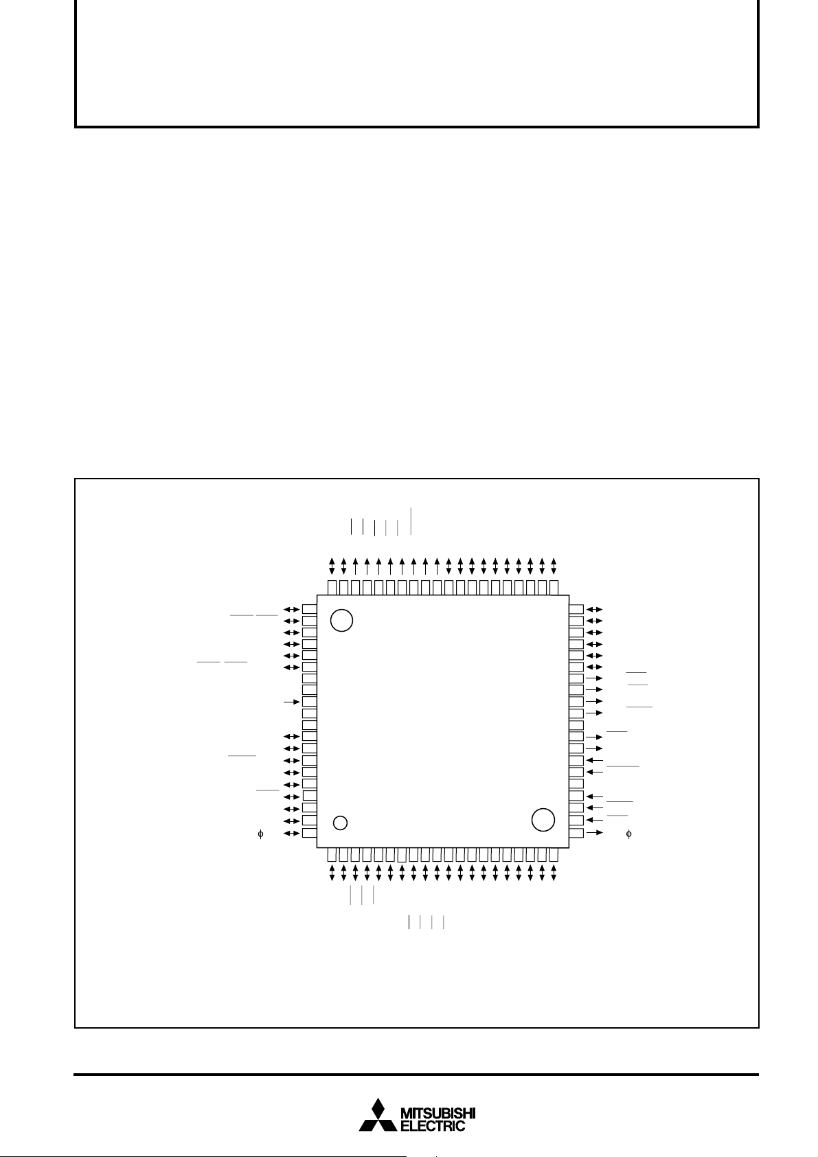
PIN CONFIGURATION (TOP VIEW)
2
1
0
D1
xD1
6/R
P8
7/Tx
P8
0/CS
P0
1/CS
P0
2/CS
P0
16-BIT CMOS MICROCOMPUTER
●Interrupts ............................................................ 19 types, 7 levels
●Multiple-function 16-bit timer ................................................. 5 + 3
●Serial I/O (UART or clock synchronous)..........................................3
●10-bit A-D converter ..............................................8-channel inputs
●12-bit watchdog timer
●Programmable input/output
(ports P4, P5, P6, P7, P8) ..............................................................37
●Clock generating circuit ........................................ 2 circuits built-in
●Small package.......................80-pin plastic molded fine-pitch QFP
(80P6D-A; 0.5 mm lead pitch)
APPLICATION
Control devices for general commercial equipment such as office
automation, office equipment, and so on.
Control devices for general industrial equipment such as
communication equipment, and so on.
11
12
3
3/CS
P0
4
4/CS
P0
RSMP
5/
P0
16
A
6/
P0
17
A
7/
P0
8
/D
8
/A
0
P1
9
/D
9
/A
1
P1
10
/D
10
/A
2
P1
/D
11
/A
3
P1
/D
12
/A
4
P1
13
/D
13
/A
5
P1
14
/D
14
/A
6
P1
15
/D
15
/A
7
P1
0
/D
0
/A
0
P2
1
/D
1
/A
1
P2
P8
0
P7
P8
/CTS
5/AN
P8
P6
P7
2
P7
P7
/R
0
P7
5/
P7
4
/CTS
X
/RTS
6
/AN
AD
4
/AN
3
/AN
2
/TB2
7
P8
D
P8
7
/AN
P8
/AN
5
/CLK
1
/RTS
3
/T
/CLKS
0
1
/CLK
/CLKS
0
7
/X
6
TRG
/R
4
/CLK
3
/CTS
2
1
P7
0
P7
/
IN
X
V
AV
V
AV
V
/X
COUT
X
/T
X
/AN
/AN
D
CC
CC
REF
SS
CIN
D
D
SUB
59
57
58
60
61
1
62
1
0
63
0
64
65
0
66
1
67
68
69
70
SS
71
72
73
74
2
75
2
76
2
77
2
78
1
79
0
80
3
2
1
4
1
2
IN
IN
/INT
/INT
3
4
/TB1
/TB0
6
5
P6
P6
P6
P6
53
55
54
56
M37735S4LHP
5
8
7
6
3
0
IN
OUT
/INT
2
/RTP1
1/TA4
3
P6
0/TA4
P6
/KI
P6
IN
/TA3
7
P5
52
9
2
/RTP1
2
/KI
OUT
6/TA3
P5
51
10
1
/RTP1
/KI1
IN
/TA2
5
P5
50
11
0
/RTP1
/KI0
OUT
4/TA2
P5
49
47
45
46
48
16
14
13
12
15
0
1
2
3
7
P4
/RTP0
/RTP0
/RTP0
/RTP0
IN
IN
OUT
OUT
/TA1
/TA0
2/TA1
0/TA0
P53
P51
P5
P5
41
42
43
44
40
39
38
37
36
35
34
33
32
31
30
29
28
27
26
25
24
23
22
21
20
18
17
19
6
2
/A
P2
/A
3
P2
4
/A
P2
/A
5
P2
/A
6
P2
P2
7
/A
P3
/WEL
0
1
/WEH
P3
/ALE
2
P3
/HLDA
3
P3
SS
V
RDE
OUT
X
IN
X
RESET
SS
CNV
BYTE
HOLD
RDY
/
2
P4
2
2
/D
3
/D
3
4
4
/D
5
/D
5
6
6
/D
7
7
/D
1
P43P44P45P4
Outline 80P6D-A
MITSUBISHI MICROCOMPUTERS
X
IN
X
OUT
RESET
Reset input
V
REF
P8(8) P7(8) P5(8) P6(8) P4(5)
Address (18)/Data (16)
CNVss
BYTE
UART1(9)
UART0(9)
AV
SS
(0V)
AV
CC
(0V)
V
SS
V
CC
A-D Converter(10)
X
CIN
X
COUT
X
CIN
X
COUT
Clock input Clock output
Reference
voltage input
External data bus width
selection input
Clock Generating Circuit
Instruction Register(8)
Arithmetic Logic
Unit(16)
Accumulator A(16)
Accumulator B(16)
Index Register X(16)
Index Register Y(16)
Stack Pointer S(16)
Direct Page Register DPR(16)
Input Butter Register IB(16)
Data Bank Register DT(8)
Program Bank Register PG(8)
Incrementer/Decrementer(24)
Data Address Register DA(24)
Incrementer(24)
Instruction Queue Buffer Q
2
(8)
Instruction Queue Buffer Q
1
(8)
Instruction Queue Buffer Q
0
(8)
Data Buffer DB
L
(8)
Data Buffer DB
H
(8)
RAM
2048 bytes
Timer TA3(16)
Timer TA4(16)
Timer TA2(16)
Timer TA1(16)
Timer TA0(16)
Watchdog Timer
Timer TB2(16)
Timer TB1(16)
Timer TB0(16)
Address Bus
Data Bus(Odd)
Data Bus(Even)
Input/Output
port P8
Input/Output
port P7
Input/Output
port P6
Input/Output
port P5
Input/Output
port P4
Address bus/Data bus
UART2(9 )
WEL
WEHALEHLDAHOLDRDY
1
RDE
RSMP
CS
0
CS
1
CS
2
CS
3
CS
4
Processor Status Register PS(11)
Program Counter PC(16)
Program Address Register PA(24)
M37735S4LHP
New product
16-BIT CMOS MICROCOMPUTER
M37735S4LHP BLOCK DIAGRAM
2
MITSUBISHI MICROCOMPUTERS
M37735S4LHP
New product
16-BIT CMOS MICROCOMPUTER
FUNCTIONS OF M37735S4LHP
Parameter Functions
Number of basic instructions 103
Instruction execution time 333 ns (the fastest instruction at external clock 12 MHz frequency)
Memory size RAM 2048 bytes
Input/Output ports
Multi-function timers
Serial I/O (UART or clock synchronous serial I/O) ✕ 3
A-D converter 10-bit ✕ 1 (8 channels)
Watchdog timer 12-bit ✕ 1
Interrupts
Clock generating circuit
Supply voltage 2.7 – 5.5 V
Power dissipation
Input/Output characteristic
Memory expansion Maximum 1 Mbytes
Operating temperature range –40 to 85 °C
Device structure CMOS high-performance silicon gate process
Package 80-pin plastic molded fine-pitch QFP (80P6D-A; 0.5 mm lead pitch)
P5 – P8 8-bit ✕ 4
P4 5-bit ✕ 1
TA0, TA1, TA2, TA3, TA4 16-bit ✕ 5
TB0, TB1, TB2 16-bit ✕ 3
3 external types, 16 internal types
Each interrupt can be set to the priority level (0 – 7.)
2 circuits built-in (externally connected to a ceramic resonator or a
quartz-crystal oscillator)
10.8 mW (at 3 V supply voltage, external clock 12 MHz frequency)
27 mW (at 5 V supply voltage, external clock 12 MHz frequency)
Input/Output voltage 5 V
Output current 5 mA
3
MITSUBISHI MICROCOMPUTERS
M37735S4LHP
New product
16-BIT CMOS MICROCOMPUTER
PIN DESCRIPTION
Pin Name Input/Output Functions
Vcc, Power source Apply 2.7 – 5.5 V to Vcc and 0 V to Vss.
Vss
CNVss CNVss input Input Connect to Vcc.
_____
RESET Reset input Input When “L” level is applied to this pin, the microcomputer enters the reset state.
XIN Clock input Input
XOUT Clock output Output
___
RDE
BYTE
Read enable output
Bus width
Output
Input This pin determines whether the external data bus has an 8-bit width or a 16-bit width.
selection input The data bus has a 16-bit width when “L” signal is input and an 8-bit width when “H” signal
AVcc, Analog power Power source input pin for the A-D converter. Externally connect AVcc to Vcc and AVss to Vss.
AVss source input
V
REF Reference Input This is reference voltage input pin for the A-D converter.
voltage input
___
P00/CS0 – Chip selection Output
___
P04/CS4 output
____
P05/RSMP
Ready sampling
Output
output
P06/A16,
Address output
Output An address (A16, A17) is output.
P07/A17
P10/A8/D8 – Address output
P17/A15/D15/data
(high
I/O When the BYTE pin is set
-order) I/O
P20/A0/D0 –
P27/A7/D7
P30/WEL Write enable Output
___
Address output
/data (low
-order) I/O
I/O Low-order data (D0 – D7) is input/output or an address (A0 – A7) is output.
output is “L”. When the BYTE pin is “H” and writing to an even address or an odd address is performed,
___
P31/WEH Write enable Output
high output
P3
2/ALE Address latch Output This is used to retrieve only the address from the multiplex signal which consists of address and
enable output data.
____
P33/HLDA Hold acknow- Output This outputs “L” level when the microcomputer enters hold state after a hold request is accepted.
____
HOLD Hold request Input
___
RDY Ready input Input
ledge output
input signal is “L”.
These are pins of main-clock generating circuit. Connect a ceramic resonator or a quartz-crystal
oscillator between X
connected to the XIN pin, and the XOUT pin should be left open.
When data/instruction read is performed, output level of RDE signal is “L”.
IN and XOUT. When an external clock is used, the clock source should be
___
is input.
___
When the specified external memory area is accessed, CS0 – CS4 signals are “L”.
The timing signal to be input to the RDY pin is output.
to
___
“L”
and
external data bus has a 16-bit width, high-order data
___
(D8 – D15) is input/output or an address (A8 – A15) is output. When the BYTE pin is “H” and an
external data bus has an 8-bit width, only address (A8 – A15) is output.
When the BYTE pin is “L” and writing to an even address is performed, output level of WEL signal
output level of WEL signal is “L”.
When the BYTE pin is “L” and writing to an odd address is performed, output level of WEH signal
is “L”. When the BYTE pin is “H”, WEH signal is always “H”.
This is an input pin for HOLD request signal. The microcomputer enters hold state while this
This is an input pin for RDY signal. The microcomputer enters ready state while this signal is “L”.
___
___
____
___
___
___
P42/ 1 Clock output Output This pin outputs the clock 1.
P4
3 – P47 I/O port P4 I/O These pins become a 5-bit I/O port. An I/O direction register is available so that each pin can be
programmed for input or output. These ports are in the input mode when reset.
P5
0 – P57 I/O port P5 I/O In addition to having the same functions as port P4, these pins also function as I/O pins for timers
A0 to A3 and input pins for key input interrupt input (KI0 – KI3).
P6
0 – P67 I/O port P6 I/O In addition to having the same functions as port P4, these pins also function as I/O pins for timer
A4, input pins for external interrupt input (INT0 – INT2) and input pins for timers B0 to B2. P67 also
___ ___
__ __
functions as sub-clock SUB output pin.
P7
0 – P77 I/O port P7 I/O In addition to having the same functions as port P4, these pins function as input pins for A-D
converter. P72 to P75 also function as I/O pins for UART2. Additionally, P76 and P77 have the
function as the output pin (XCOUT) and the input pin (XCIN) of the sub-clock (32 kHz) oscillation
circuit, respectively. When P76 and P77 are used as the XCOUT and XCIN pins, connect a resonator
or an oscillator between the both.
P80 – P87 I/O port P8 I/O In addition to having the same functions as port P4, these pins also function as I/O pins for UART
0 and UART 1.
4
MITSUBISHI MICROCOMPUTERS
M37735S4LHP
New product
BASIC FUNCTION BLOCKS
The M37735S4LHP has the same functions as the M37735MHBXXXFP
except for the following:
(1) The memory map is different.
(2) The processor mode is different.
(3) The reset circuit is different.
(4) Pulse output port mode of timer A is available.
(5) The function of ROM area modification is not available.
Refer to the section on the M37735MHBXXXFP, except for above
(1)–(5).
MEMORY
The memory map is shown in Figure 1. The address space has a
capacity of 16 Mbytes and is allocated to addresses from 0
FFFFFF
16. The address space is divided by 64-Kbyte unit called bank.
The banks are numbered from 0
However, banks 10
16–FF16 of the M37735S4LHP cannot be
16 to FF16.
accessed.
000000
16
Bank 0
16
00FFFF
16
010000
16
16 to
000000
00007F
000080
16-BIT CMOS MICROCOMPUTER
Built-in RAM and control registers for internal peripheral devices are
assigned to bank 0
Addresses FFD6
addresses and contain the interrupt vectors. Use ROM for memory
of this address.
The 2048-byte area allocated to addresses from 80
built-in RAM. In addition to storing data, the RAM is used as stack
during a subroutine call or interrupts.
Peripheral devices such as I/O ports, A-D converter, serial I/O, timer,
and interrupt control registers are allocated to addresses from 0
7F
16.
A 256-byte direct page area can be allocated anywhere in bank 0
by using the direct page register (DPR). In the direct page addressing
mode, the memory in the direct page area can be accessed with two
words. Hence program steps can be reduced.
16
16
16
Internal RAM
2048 bytes
16.
16 to FFFF16 are the RESET and interrupt vector
16 to 87F16 is the
000000
16
Internal peripheral
devices
control registers
refer to Fig. 2 for
detail information
00007F
16
16 to
16
Bank 1
16
• • • • • • • • • • • • • • • • • • •
Bank FE
16
Bank FF
16
00087F
00FFD6
00FFFF
16
16
16
01FFFF
FE0000
FEFFFF
FF0000
FFFFFF
16
16
16
16
16
: Internal
: External
Note. Banks 1016–FF16 cannot be accessed in the M37735S4LHP.
00FFD6
00FFFE
Interrupt vector table
16
A-D/UART2 trans./rece.
UART1 transmission
UART1 receive
UART0 transmission
UART0 receive
Timer B2
Timer B1
Timer B0
Timer A4
Timer A3
Timer A2
Timer A1
Timer A0
INT
2
/Key input
INT
1
INT
0
Watchdog timer
DBC
BRK instruction
Zero divide
16
RESET
Fig. 1 Memory map
5
MITSUBISHI MICROCOMPUTERS
M37735S4LHP
New product
Address (Hexadecimal notation)
000000
000001
000002
000003
000004
000005
000006
000007
000008
000009
00000A
00000B
00000C
00000D
00000E
00000F
000010
000011
000012
000013
000014
000015
000016
000017
000018
000019
00001A
00001B
00001C
00001D
00001E
00001F
000020
000021
000022
000023
000024
000025
000026
000027
000028
000029
00002A
00002B
00002C
00002D
00002E
00002F
000030
000031
000032
000033
000034
000035
000036
000037
000038
000039
00003A
00003B
00003C
00003D
00003E
00003F
Port P0 register
Port P1 register
Port P0 direction register
Port P1 direction register
Port P2 register
Port P3 register
Port P2 direction register
Port P3 direction register
Port P4 register
Port P5 register
Port P4 direction register
Port P5 direction register
Port P6 register
Port P7 register
Port P6 direction register
Port P7 direction register
Port P8 register
Port P8 direction register
Pulse output data register 1
Pulse output data register 0
A-D control register 0
A-D control register 1
A-D register 0
A-D register 1
A-D register 2
A-D register 3
A-D register 4
A-D register 5
A-D register 6
A-D register 7
UART 0 transmit/receive mode register
UART 0 baud rate register (BRG0)
UART 0 transmission buffer register
UART 0 transmit/receive control register 0
UART 0 transmit/receive control register 1
UART 0 receive buffer register
UART 1 transmit/receive mode register
UART 1 baud rate register (BRG1)
UART 1 transmission buffer register
UART 1 transmit/receive control register 0
UART 1 transmit/receive control register 1
UART 1 receive buffer register
16-BIT CMOS MICROCOMPUTER
Address (Hexadecimal notation)
000040
Count start flag
000041
000042
One-shot start flag
000043
000044
Up-down flag
000045
000046
000047
000048
000049
00004A
00004B
00004C
00004D
00004E
00004F
000050
000051
000052
000053
000054
000055
000056
000057
000058
000059
00005A
00005B
00005C
00005D
00005E
00005F
000060
000061
000062
000063
000064
000065
000066
000067
000068
000069
00006A
00006B
00006C
00006D
00006E
00006F
000070
000071
000072
000073
000074
000075
000076
000077
000078
000079
00007A
00007B
00007C
00007D
00007E
00007F
Timer A0 register
Timer A1 register
Timer A2 register
Timer A3 register
Timer A4 register
Timer B0 register
Timer B1 register
Timer B2 register
Timer A0 mode register
Timer A1 mode register
Timer A2 mode register
Timer A3 mode register
Timer A4 mode register
Timer B0 mode register
Timer B1 mode register
Timer B2 mode register
Processor mode register 0
Processor mode register 1
Watchdog timer register
Watchdog timer frequency selection flag
Waveform output mode register
Reserved area (Note)
UART2 transmit/receive mode register
UART2 baud rate register (BRG2)
UART2 transmission buffer register
UART2 transmit/receive control register 0
UART2 transmit/receive control register 1
UART2 receive buffer register
Oscillation circuit control register 0
Port function control register
Serial transmit control register
Oscillation circuit control register 1
A-D/UART2 trans./rece. interrupt control register
UART 0 transmission interrupt control register
UART 0 receive interrupt control register
UART 1 transmission interrupt control register
UART 1 receive interrupt control register
Timer A0 interrupt control register
Timer A1 interrupt control register
Timer A2 interrupt control register
Timer A3 interrupt control register
Timer A4 interrupt control register
Timer B0 interrupt control register
Timer B1 interrupt control register
Timer B2 interrupt control register
INT
0
interrupt control register
INT
1
interrupt control register
INT
2
/Key input interrupt control register
Note. Writing to reserved area is disabled.
Fig. 2 Location of internal peripheral devices and interrupt control registers
6
MITSUBISHI MICROCOMPUTERS
M37735S4LHP
New product
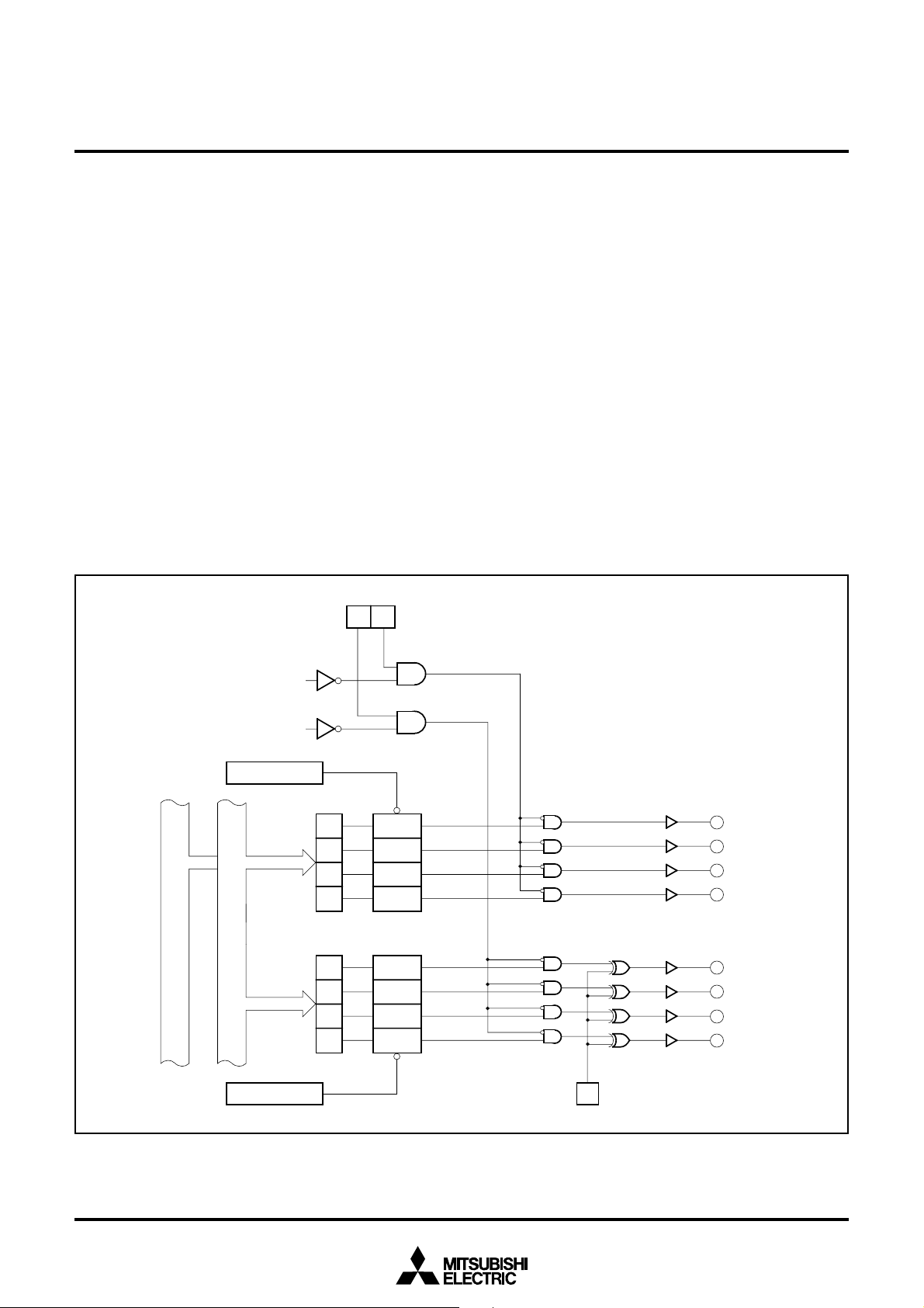
Pulse output port mode
The pulse motor drive waveform can be output by using plural internal
timer A.
Figure 3 shows a block diagram for pulse output port mode. In the
pulse output port mode, two pairs of four-bit pulse output ports are
used. Whether using pulse output port or not can be selected by
waveform output selection bit (bit 0, bit 1) of waveform output mode
register (62
output selection bit is set to “1”, RTP1
are used as pulse output ports, and when bit 1 of waveform output
selection bit is set to “1”, RTP0
used as pulse output ports. When bits 1 and 0 of waveform output
selection bit are set to“1”, RTP1
RTP0
The ports not used as pulse output ports can be used as normal
parallel ports, timer input/output or key input interruput input.
In the pulse output port mode, set timers A0 and A2 to timer mode as
timers A0 and A2 are used. Figure 5 shows the bit configuration of
timer A0, A2 mode registers in pulse output port mode.
Data can be set in each bit of the pulse output data register
corresponding to four ports selected as pulse output ports. Figure 6
16 address) shown in Figure 4. When bit 0 of waveform
0, RTP11, RTP12, and RTP13
0, RTP01, RTP02, and RTP03 are
0, RTP11, RTP12, and RTP13, and
0, RTP01, RTP02, and RTP03 are used as pulse output ports.
16-BIT CMOS MICROCOMPUTER
shows the bit configuration of the pulse output data register. The
contents of the pulse output data register 1 (low-order four bits of
1C
16 address) corresponding to RTP10, RTP11, RTP12, and RTP13
is output to the ports each time the counter of timer A2 becomes
0000
16. The contents of the pulse output data register 0 (low-order
four bits of 1D
and RTP0
becomes 0000
Figure 7 shows example of waveforms in pulse output port mode.
When “0” is written to a specified bit of the pulse output data register,
“L” level is output to the corresponding pulse output port when the
counter of corresponding timer becomes 0000
written, “H” level is output to the pulse output port.
Pulse width modulation can be applied to each pulse output port.
Since pulse width modulation involves the use of timers A1 and A3,
activate these timers in pulse width modulation mode.
16 address) corresponding to RTP00, RTP01, RTP02,
3 is output to the ports each time the counter of timer A0
16.
16, and when “1” is
Pulse width modulation selection bit
(Bit 4, 5 of 62
16
address)
Pulse width modulation output
by timer A3
Pulse width modulation output
by timer A1
Timer A2
Pulse output data
register 1 (1C16 address)
Data bus (even)
Data bus (odd)
Pulse output data
register 0 (1D
Timer A0
3
D
D
2
D
1
D
0
D
11
D
10
D
9
D
8
16
address)
45
T
D
D
D
D
D
D
D
D
T
Q
Q
Q
Q
Q
Q
Q
Q
Polarity selection bit
(Bit 3 of 62
16
address)
3
(P57)
RTP1
RTP1
2
(P56)
RTP1
1
(P55)
RTP1
0
(P54)
RTP0
3
(P53)
RTP02 (P52)
RTP0
1
(P51)
RTP0
0
(P50)
Fig. 3 Block diagram for pulse output port mode
7
MITSUBISHI MICROCOMPUTERS
M37735S4LHP
New product
RTP10, RTP11, RTP12, and RTP13 are applied pulse width modulation
by timer A3 by setting the pulse width modulation selection bit by
timer A3 (bit 5) of the waveform output mode register to “1”.
RTP0
0, RTP01, RTP02, and RTP03 are applied pulse width modulation
by timer A1 by setting the pulse width modulation selection bit by
timer A1 (bit 4) of the waveform output mode register to “1”.
The contents of the pulse output data register 0 can be reversed and
output to pulse output ports RTP0
the polarity selection bit (bit 3) of the waveform output mode register.
When the polarity selection bit is “0”, the contents of the pulse output
data register 0 is output unchangeably, and when “1”, the contents of
the pulse output data register 0 is reversed and output. When pulse
width modulation is applied, likewise the polarity reverse to pulse
width modulation can be selected by the polarity selection bit.
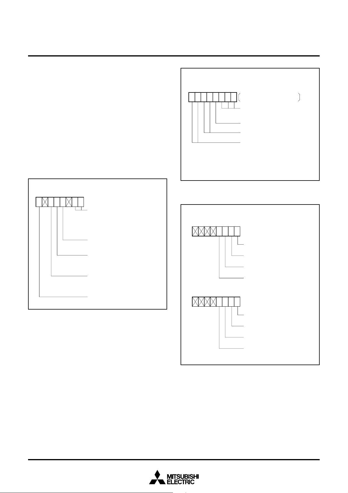
765432 01
0
0, RTP01, RTP02, and RTP03 by
Address
Weveform output mode register 6216
Weveform output selection bit
0 0 : Parallel port
0 1 : RTP1 selected
1 0 : RTP0 selected
1 1 : RTP1 and RTP0 selected
Polarity selection bit
0 : Positive polarity
1 : Negative polarity
Pulse width modulation selection bit
by timer A1
0 : Not modulated
1 : Modulated
Pulse width modulation selection bit
by timer A3
0 : Not modulated
1 : Modulated
Always “0”
16-BIT CMOS MICROCOMPUTER
765432 01
0 0 X 1 0 0
Timer A0 mode register 5616
Timer A2 mode register 5816
Always “100” in pulse output
port mode
Not used in pulse output port mode
Always “00” in pulse output port mode
Clock source selection bit
0 0 : Select f
0 1 : Select f16
1 0 : Select f64
1 1 : Select f512
2
Fig. 5 Timer A0, A2 mode register bit configuration in pulse output
port mode
765432 01
Pulse output data register 0 1D16
RTP00 output data
RTP01 output data
RTP02 output data
RTP03 output data
765432 01
Pulse output data register 1 1C16
Address
Address
Address
Fig. 4 Waveform output mode register bit configuration
8
0
output data
RTP1
RTP11 output data
RTP12 output data
RTP13 output data
Fig. 6 Pulse output data register bit configuration
MITSUBISHI MICROCOMPUTERS
M37735S4LHP
New product
Output signal at each time
when timer A2 becomes 0000
3 (P57)
RTP1
RTP1
2 (P56)
1 (P55)
RTP1
RTP10 (P54)
Output signal at each time
when timer A2 becomes 0000
16-BIT CMOS MICROCOMPUTER
Example of pulse output port (RTP10 – RTP13)
16
Example of pulse output port (RTP10 – RTP13) when pulse width modulation is applied by timer A3.
16
3 (P57)
RTP1
RTP1
2 (P56)
1 (P55)
RTP1
0 (P54)
RTP1
Output signal at each time
when timer A0 becomes 0000
RTP0
3 (P53)
RTP0
2 (P52)
1 (P51)
RTP0
Example of pulse output port (RTP00 – RTP03) when pulse width modulation is applied
by timer A1 with polarity selection bit = “1”.
16
0 (P50)
RTP0
Fig. 7 Example of waveforms in pulse output port mode
9
MITSUBISHI MICROCOMPUTERS
M37735S4LHP
New product
PROCESSOR MODE
Only the microprocessor mode can be selected.
Figure 9 shows the functions of pins P00/CS0 — P47 in the
microprocessor mode.
Figure 10 shows external memory area for the microprocessor mode.
Access to the external memory is affected by the BYTE pin, the wait
bit (bit 2 of the processor mode register 0 at address 5E
wait selection bit (bit 0 of the processor mode register 1 at address
5F
16) .
765432 01
0
10
Processor mode register 0
Must be “10” (“10” after reset)
Wait bit
0 : Wait
1 : No wait
___
16), and the
Address
16
5E
16-BIT CMOS MICROCOMPUTER
• BYTE pin
When accessing the external memory, the level of the BYTE pin is
used to determine whether to use the data bus as 8-bit width or 16bit width.
The data bus has a width of 8 bits when level of the BYTE pin is “H”,
and pins P2
The data bus has a width of 16 bits when the level of the BYTE pin is
“L”, and pins P2
D
15 are the data I/O pins.
When accessing the internal memory, the data bus always has a
width of 16 bits regardless of the BYTE pin level.
765432 01
0/A0/D0 — P27/A7/D7 are the data I/O pins.
0/A0/D0 — P27/A7/D7 and pins P10/A8/D8 — P17/A15/
Address
Processor mode register 1
Wait selection bit
0 : Wait 0
1 : Wait 1
5F16
Software reset bit
Reset occurs when this bit is set to “1”
Interrupt priority detection time selection bit
0 0 : Internal clock ✕ 7 (cycle)
0 1 : Internal clock
1 0 : Internal clock ✕ 2 (cycle)
Must be “0”
Not used
Fig. 8 Processor mode register bit configuration
✕ 4 (cycle)
10
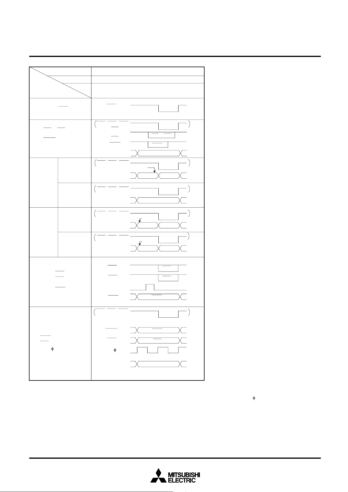
MITSUBISHI MICROCOMPUTERS
M37735S4LHP
New product
PM1
PM0
Mode
Pin
RDE
0 to CS4
CS
RSMP,
A16, A17
BYTE = “L”
P10/A8/D8
to
P17/A15/D15
BYTE = “H”
BYTE = “L”
P20/A0/D0
to
P27/A7/D7
BYTE = “H”
RDE
RDE, WEL, WEH
P00/CS0
to
P04/CS4
P05/RSMP
P06/A16
P07/A17
RDE, WEL, WEH
P10/A8/D8
to
7/A15 /D15
P1
RDE, WEL, WEH
P10/A8/D8
to
7/A15/D15
P1
RDE, WEL, WEH
P20/A0/D0
to
7/A7/D7
P2
RDE, WEL, WEH
P20/A0/D0
to
7/A7/D7
P2
1
0
Microprocessor mode
CS0 — CS4
RSMP
Address A16, A17
A8 to A15
Address
Data(odd)
Address A8 – A15
A0 to A7
Address
A0 to A7
Address
Data(even)
Data
(odd,even)
16-BIT CMOS MICROCOMPUTER
(Note)
0/WEL,
P3
P31/WEH,
P32/ALE,
P33/HLDA
HOLD,
,
RDY
P42/ 1,
Ports P43 to P47
P30/WEL
P31/WEH
P32/ALE
P33/HLDA
RDE, WEL, WEH
HOLD
RDY
P42/ 1
ALE
HLDA
HOLD
RDY
WEL
WEH
(Note)
(Note)
(Note)
P43
to
I/O Port
P47
Fig. 9 Functions of pins P00/CS0 to P47 in microprocessor mode
Note. The signal output disable selection bit (bit 6 of the oscillation circuit control register 0) can stop the 1 output in the microprocessor
mode. In this mode, signals RDE, WEL, WEH can also be fixed to “H” when the internal memory area is accessed.
___
___ ___ ___
11
MITSUBISHI MICROCOMPUTERS
M37735S4LHP
New product
• Wait bit
As shown in Figure 11, when the external memory area is accessed
with the wait bit (bit 2 of the processor mode register 0 at address
5E
16) cleared to “0”, the access time can be extended compared with
no wait (the wait bit is “1”).
The access time is extended in two ways and this is selected with the
wait selection bit (bit 0 of the processor mode register 1 at address
5F
16).
When this bit is “1”, the access time is 1.5 times compared to that for
no wait. When this bit is “0”, the access time is twice compared to
that for no wait.
At reset, the wait bit and the wait selection bit are “0”.
Access to internal memory area is always performed in the no wait
mode regardless of the wait bit.
The processor modes are described below.
Microprocessor
mode
0016
SFR
8016
RAM
87F16
16-BIT CMOS MICROCOMPUTER
Internal clock
Wait bit “1”
(No wait)
Wait bit “0”
(Wait 1)
Wait bit “0”
(Wait 0)
Ai/Di
RDE or
WEL, WEH
ALE
Ai/Di
RDE or
WEL, WEH
ALE
Ai/Di
RDE or
WEL, WEH
ALE
Address
Access time
Address
Address
Data
Data
Access time
Address
Access time
Data
Address
Data
Data
Address
Fig. 11 Relationship between wait bit, wait selection bit, and access time
(1) Microprocessor mode [10]
The microcomputer enters the microprocessor mode after connecting
the CNVss pin to Vcc and starting from reset.
___ ___
Pin RDE is the output pin for the read enable signal (RDE).
___
RDE is “L” during the data read term in the read cycle. When the
internal memory area is read, RDE can be fixed to “H” by setting the
signal output disable selection bit (bit 6 of the oscillation circuit control
register 0) to “1”.
___
FFFFFF16
The shaded area is the external memory area.
Note that banks 10
16 to FF16 cannot be accessed.
Fig. 10 External memory area for microprocessor mode
12

MITSUBISHI MICROCOMPUTERS
M37735S4LHP
New product
___ ___
CS0 to CS4 are the chip select signals and are “L” when the address
shown in Table 2 is accessed. RSMP is the ready-sampling signal
which is output for the RDY input described later when the external
memory area is accessed. By inputting logical AND of RSMP and
___ ____
CSn (n = 0 to 4) to the RDY pin, read/write term for any address areas
___
can be extended by 1 cycle of clock
term can also be extended by 2 cycles of clock
function and wait 0/1 function specified with the wait bit are used
together.
Pins P1
0/A8/D8 — P17/A15/D15 have two functions depending on the
level of the BYTE pin.
When the BYTE pin level is “L”, pins P1
as address (A8 to A15) output pins while RDE or WEL, WEH are “H”
and as odd address data I/O pins while these signals are “L”. However,
if an internal memory is read, external data is ignored while RDE is
“L”.
When the BYTE pin level is “H”, pins P1
as address (A
Pins P2
8 to A15) output pins.
0/A0/D0 — P27/A7/D7 have two functions depending on the
level of the BYTE pin.
When the BYTE pin level is “L”, pins P2
as address (A0 to A7) output pins while RDE or WEL, WEH are “H” and
as even address data I/O pins while these signals are “L”. However,
if an internal memory is read, external data is ignored while RDE is
“L”.
When the BYTE pin level is “H”, pins P2
as address (A0 to A7) output pins while RDE or WEL, WEH are “H” and
as even and odd address data I/O pins while these signals are “L”.
However, if an internal memory is read, external data is ignored while
___
RDE is “L”.
___ ___
WEL, WEH are the write-enable low signal and the write-enable high
signal, respectively. These signals are “L” during the data write term
of the write cycle, but their operations differ depending on the BYTE
pin level.
In the case the BYTE pin level is “L”, WEL is “L” when writing to
an even address, WEH is “L” when writing to an odd address, and
___ ___
both WEL and WEH are “L” when writing to even and odd addresses.
In the case the BYTE pin level is “H”, regardless of address, only
___ ___ ___ ___
WEL is “L”, and WEH retains “H”. WEL and WEH can also be fixed to
___
“H” when the internal memory is accessed, same as RDE, by writing
“1” to the signal output disable selection bit.
ALE is an address latch enable signal used to latch the address signal
from a multiplexed signal of address and data. The latch is transparent
while ALE is “H” to let the address signal pass through and held
while ALE is “L”.
____
HLDA is a hold acknowledge signal and is used to notify externally
when the microcomputer receives HOLD input and enters into hold
state.
____
HOLD is a hold request signal. It is an input signal used to put the
microcomputer in hold state. HOLD input is accepted when the internal
clock falls from “H” level to “L” level while the bus is not used.
Pins P00/CS0 — P31/WEH and RDE are floating while the microcomputer
___
____
stays in hold state. After HLDA signal changes to “L” level and one
cycle of internal clock passed, these ports become floating. After
____
HLDA signal changes to “H” level and one cycle of internal clock
passed, these ports are released from floating state.
____
____
___
____
1. In addition, the read/write
1 if the above
0/A8/D8 — P17/A15/D15 function
___ ___ ___
0/A8/D8 — P17/A15/D15 function
0/A0/D0 — P27/A7/D7 function
___ ___ ___
0/A0/D0 — P27/A7/D7 function
___ ___ ___
___
___
____
____
___
___
16-BIT CMOS MICROCOMPUTER
___
RDY is a ready signal. If this signal goes “L”, the internal clock
stops at “L”. RDY is used when slow external memory is attached.
P4
2/ 1 pin is an output pin for clock 1. The 1 output is
independent of RDY and does not stop even when internal clock
stops because of “L” input to the RDY pin.
___
___
___
13

MITSUBISHI MICROCOMPUTERS
M37735S4LHP
New product
As shown in Table 3,
1 output can be stopped with the signal
output disable selection bit = “1”. In this case, write “1” to the port P4
direction register.
Table 1 shows the relationship between the CNVss pin input level
and the processor mode.
Table 2. Relationship between access addresses and chip-select signals CS0 to CS4
Chip-select
signal
___
CS0
___
CS1
The first half of bank 0016 except
internal memory area
The latter half of bank 0016 except
internal memory area and banks
Area
0116 to 0316.
___
CS2
___
CS3
___
CS4
Banks 0416 to 0716
Banks 0816 to 0B16
Banks 0C16 to 0F16
Table 1. Relationship between CNVss pin input levels and processor
2
CNVss Mode Description
Vcc
___ ___
Access address
Microprocessor mode
16
00 0880
to
00 7FFF
16
00 800016
to
03 FFFF
16
04 000016
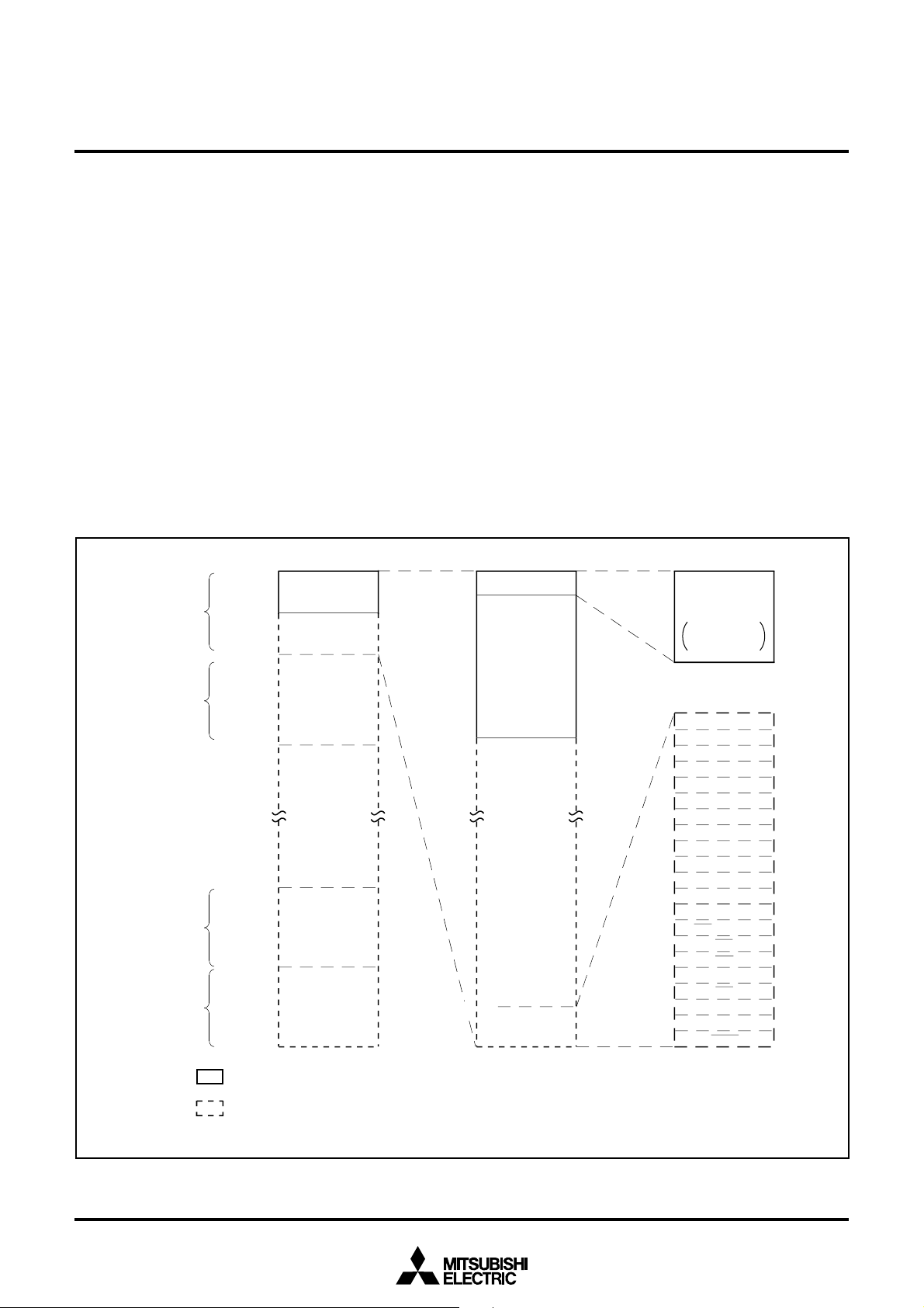
to
07 FFFF16
08 000016
to
0B FFFF
16
0C 000016
to
0F FFFF
16
mode
16-BIT CMOS MICROCOMPUTER
• Microprocessor
Microprocessor mode upon
starting after reset.
Table 3. Function of signal output disable selection bit CM6 (bit 6 of oscillation circuit control register 0)
Processor mode Pin
___
RDE,
___
WEL, WEH
___
RDE
Microprocessor mode
1
___ ___ ___
RDE, WEL, WEH are output when the
CM6 = “0” CM6 = “1”
internal/external memory area is accessed.
After WIT/STP instruction is executed,
“H” is output.
Clock
1 is output independent of 1
output selection bit.
Function
___ ___ ___
RDE, WEL, WEH are output only when the
external memory area is accessed.
“L” is output after WIT/STP instruction is
executed
∗ Standby state selection bit (bit 0 of port
function control register) must be set to “1”.
“H” or “L” is output. (Contents of P4
latch is output.)
∗ Port P4
2 direction register must be set to
2 port
“1”.
Note. Functions shown in Table 3 cannot be emulated with a debugger. For the oscillation circuit control register 0 and port function control
register, refer to Figures 64 and 11 in data sheet “M37735MHBXXXFP”, respectively.
14

MITSUBISHI MICROCOMPUTERS
M37735S4LHP
New product
RESET CIRCUIT
The microcomputer is released from the reset state when the RESET
pin is returned to “H” level after holding it at “L” level with the power
source voltage at 2.7 to 5.5 V. Program execution starts at the address
formed by setting address A
of address FFFF
16, and A7 – A0 to the contents of address FFFE16.
Figure 13 shows an example of a reset circuit. If the stabilized clock
is input from the external to the main-clock oscillation circuit, the reset
Port P0 direction register
Port P1 direction register
Port P2 direction register
Port P3 direction register
Port P4 direction register
Port P5 direction register
Port P6 direction register
Port P7 direction register
Port P8 direction register
A-D control register 0
A-D control register 1
UART 0 transmit/receive mode register
UART 1 transmit/receive mode register
UART 0 transmit/receive
control register 0
UART 1 transmit/receive
control register 0
UART 0 transmit/receive
control register 1
UART 1 transmit/receive
control register 1
Count start flag
One- shot start flag
Up-down flag
Timer A0 mode register
Timer A1 mode register
Timer A2 mode register
Timer A3 mode register
Timer A4 mode register
Timer B0 mode register
Timer B1 mode register
Timer B2 mode register
Processor mode register 0
Processor mode register 1
Watchdog timer register
23 – A16 to 0016, A15 – A8 to the contents
Address
(0416)
•••
(0516)
•••
(0816)
•••
(0916)
•••
(0C16)
•••
(0D16)
•••
(1016)
•••
(1116)
•••
(1416)
•••
(1E16)
(1F16)
(3016)
(3816)
(3416)
(3C16)
(3516)
(3D16)
(4016)
(4216)
(4416)
(5616)
(5716)
(5816)
(5916)
(5A16)
(5B16)
(5C16)
(5D16)
(5E16)
(5F16)
(6016)
•••
0000
•••
0
•••
•••
•••
•••
0000
•••
0000
•••
0000
•••
•••
•••
•••
•••
•••
•••
•••
•••
•••
001
•••
001 00 00
•••
•••
•••
FFF
00
16
00
16
00
16
0000
00
16
00
16
00
16
00
16
00
16
0
???
00
00
16
00
16
1000
000010
00
16
000 00
00
16
00
16
00
16
00
16
00
16
00
16
0001 00 00
00 00
00
16
16
_____
11
0000
0010
10
0
16-BIT CMOS MICROCOMPUTER
input voltage must be 0.55 V or less when the power source voltage
reaches 2.7 V. If a resonator/oscillator is connected to the main-clock
oscillation circuit, change the reset input voltage from “L” to “H” after
the main-clock oscillation is fully stabilized.
Figure 12 shows the status of the internal registers during reset.
Address
(6116)
(6216)
(6416)
(6816)
(6916)
(6C16)
(6D16)
(6E16)
(6F16)
(7016)
(7116)
(7216)
(7316)
(7416)
(7516)
(7616)
(7716)
(7816)
(7916)
(7A16)
(7B16)
(7C16)
(7D16)
(7E16)
(7F16)
•••
0 0 0 0 0 0
•••
•••
0 0
•••
0 0 0
•••
•••
0 0 0 0 1 0
•••
•••
•••
•••
•••
•••
•••
•••
•••
•••
•••
•••
•••
•••
•••
•••
•••
•••
•••
00
00
0
0
0
0
0
0
0
0
?
00
?000
00
Content of FFFF
Content of FFFE
0000
16
00
0 0 000
0001
0 1 0 0 0
16
000
0
0000
0000
0000
0000
0000
0000
0000
0000
0000
0000
0000
0000
0000
000
0
000
0
0 00
0
1??
0
16
16
Watchdog timer frequency selection flag
Waveform output mode register
UART2 transmit/receive mode register
UART2 transmit/receive control register 0
UART2 transmit/receive control register 1
Oscillation circuit control register 0
Port function control register
Serial transmit control register
Oscillation circuit control register 1
A-D/UART2 trans./rece. interrupt control register
UART 0 transmission interrupt control register
UART 0 receive interruupt control register
UART 1 transmission interrupt control register
UART 1 receive interruupt control register
Timer A0 interrupt control register
Timer A1 interrupt control register
Timer A2 interrupt control register
Timer A3 interrupt control register
Timer A4 interrupt control register
Timer B0 interrupt control register
Timer B1 interrupt control register
Timer B2 interrupt control register
0
interrupt control register
INT
INT1 interrupt control register
INT2/key input interrupt control register
Processor status register (PS)
Program bank register (PG)
H
Program counter (PC
Program counter (PC
Direct page register (DPR)
Data bank register (DT)
)
L
)
0
16
16
Fig. 12 Microcomputer internal status during reset
Contents of other registers and RAM are undefined during reset. Initialize them by software.
15

MITSUBISHI MICROCOMPUTERS
M37735S4LHP
New product
RESET
Note. In this case, stabilized clock is input from the
external to the main-clock oscillation circuit.
Perform careful evaluation at the system design
level before using.
Fig. 13 Example of a reset circuit
VCC
VCC
0 V
RESET
0 V
Power on
2.7 V
0.55 V
16-BIT CMOS MICROCOMPUTER
ADDRESSING MODES
The M37735S4LHP has 28 powerful addressing modes.Refer to the
MITSUBISHI SEMICONDUCTORS DATA BOOK SINGLE-CHIP 16BIT MICROCOMPUTERS for the details of each addressing mode.
MACHINE INSTRUCTION LIST
The M37735S4LHP has 103 machine instructions. Refer to the
MITSUBISHI SEMICONDUCTORS DATA BOOK SINGLE-CHIP 16BIT MICROCOMPUTERS for details.
16

MITSUBISHI MICROCOMPUTERS
M37735S4LHP
New product
16-BIT CMOS MICROCOMPUTER
ABSOLUTE MAXIMUM RATINGS
Symbol Parameter Conditions Ratings Unit
Vcc Power source voltage –0.3 to +7 V
AVcc Analog power source voltage –0.3 to +7 V
VI
Input voltage RESET, CNVss, BYTE –0.3 to +12 V
Input voltage
VI
Output voltage
VO
_____
P10/A8/D8 – P17/A15/D15, P20/A0/D0 – P27/A7/D7,
P4
3 – P47, P50 – P57, P60 – P67, P70 – P77,
P80 – P87, VREF, XIN, HOLD, RDY
___
P00/CS0 – P07/A17, P10/A8/D8 – P17/A15/D15,
P20/A0/D0 – P27/A7/D7, P30/WEL – P33/HLDA ,P42/ 1,
P4
3 – P47, P50 – P57, P60 – P67, P70 – P77, P80 – P87,
___
XOUT, RDE
____
___
___ ____
–0.3 to Vcc + 0.3 V
–0.3 to Vcc + 0.3 V
Pd Power dissipation Ta = 25 °C 200 mW
Topr Operating temperature –40 to +85 °C
T
stg Storage temperature –65 to +150 °C
RECOMMENDED OPERATING CONDITIONS (Vcc = 2.7 – 5.5 V, Ta = –40 to +85 °C, unless otherwise noted)
Limits
___
Vcc
Vcc
0.2Vcc
0.16Vcc
–10
–5
10
16
5
____
HLDA
and P8 must
Unit
V
V
V
V
V
mA
mA
mA
mA
mA
___
Vcc Power source voltage
ParameterSymbol
f(XIN) : Operating 2.7 5.5
f(XIN) : Stopped, f(XCIN) = 32.768 kHz 2.7 5.5
Min. Typ. Max.
AVcc Analog power source voltage Vcc V
Vss Power source voltage 0V
AVss Analog power source voltage 0 V
V
VIH
VIL
VIL
IH
High-level input voltage
High-level input voltage P10/A8/D8 – P17/A15/D15, P20/A0/D0 – P27/A7/D7
Low-level input voltage
Low-level input voltage P10/A8/D8 – P17/A15/D15, P20/A0/D0 – P27/A7/D7
High-level peak output current P00/CS0 – P07/A17, P10/A8/D8 – P17/A15/D15,
IOH(peak)
High-level average output current P00/CS0 – P07/A17, P10/A8/D8 – P17/A15/D15,
IOH(avg)
Low-level peak output current P00/CS0 – P07/A17, P10/A8/D8 – P17/A15/D15,
IOL(peak)
____ ___
HOLD, RDY, P43 – P47, P50 – P57, P60 – P67, P70 – P77,
P80 – P87, XIN, RESET, CNVss, BYTE, XCIN (Note 3)
____ ___
HOLD, RDY, P43 – P47, P50 – P57, P60 – P67, P70 – P77,
P80 – P87, XIN, RESET, CNVss, BYTE, XCIN (Note 3)
_____
_____
___
P20/A0/D0 – P27/A7/D7, P30/WEL – P33/
P4
2/ 1, P43 – P47, P50 – P57, P60 – P67,
P70 – P77, P80 – P87
___
P20/A0/D0 – P27/A7/D7, P30/WEL – P33/
P4
2/ 1, P43 – P47, P50 – P57, P60 – P67,
P70 – P77, P80 – P87
___
P20/A0/D0 – P27/A7/D7, P30/WEL – P33/
P4
2/ 1, P43, P54 – P57, P60 – P67, P70 – P77,
___
___
___
____
HLDA
____
HLDA
,
____
HLDA
,
0.8 Vcc
0.5 Vcc
0
0
,
P80 – P87
IOL(peak)
IOL(avg)
Low-level peak output current P44 – P47, P50 – P53
Low-level average output current P00/CS0 – P07/A17, P10/A8/D8 – P17/A15/D15,
___
P20/A0/D0 – P27/A7/D7, P30/WEL – P33/
P4
2/ 1, P43, P54 – P57,P60 – P67, P70 – P77,
___
____
HLDA
,
P80 – P87
IOL(avg) Low-level average output current P44 – P47, P50 – P53 12 mA
f(XIN) Main-clock oscillation frequency (Note 4) 12 MHz
f(X
CIN) Sub-clock oscillation frequency 32.768 50 kHz
Notes 1. Average output current is the average value of a 100 ms interval.
2. The sum of IOL(peak) for ports P00/CS0 – P07/A17, P10/A8/D8 – P17/A15/D15, P20/A0/D0 – P27/A7/D7, P30/WEL – P33/
be 80 mA or less, the sum of IOH(peak) for ports P00/CS0 – P07/A17, P10/A8/D8 – P17/A15/D15, P20/A0/D0 – P27/A7/D7, P30/WEL – P33/
____
HLDA
and P8 must be 80 mA or less, the sum of IOL(peak) for ports P4, P5, P6, and P7 must be 100 mA or less, and the sum of IOH(peak)
___
___
for ports P4, P5, P6, and P7 must be 80 mA or less.
3. Limits V
4. The maximum value of f(X
IH and VIL for XCIN are applied when the sub clock external input selection bit = “1”.
IN) = 6 MHz when the main clock division selection bit = “1”.
17

MITSUBISHI MICROCOMPUTERS
M37735S4LHP
New product
16-BIT CMOS MICROCOMPUTER
ELECTRICAL CHARACTERISTICS (Vcc = 5 V, Vss = 0 V, Ta = –40 to +85 °C, f(XIN) = 12 MHz, unless otherwise noted)
Symbol Parameter Test conditions
___
P20/A0/D0 – P27/A7/D7, P33/HLDA, P42/
____
P43 – P47, P50 – P57, P60 – P67, P70 – P77,
P8
0 – P87
___
P20/A0/D0 – P27/A7/D7, P33/HLDA, P42/
___
____
____
VCC = 5 V, IOH = –10 mA
1,
CC = 3 V, IOH = –1 mA
V
V
CC = 5 V, IOH = –400 A
1
VCC = 5 V, IOH = –10 mA
VCC = 5 V, IOH = –400 A
V
OH
VOH
VOH
High-level output voltage P00/CS0 – P07/A17, P10/A8/D8 – P17/A15/D15,
High-level output voltage P00/CS0 – P07/A17, P10/A8/D8 – P17/A15/D15,
High-level output voltage P30/WEL, P31/WEH, P32/ALE
VCC = 3 V, IOH = –1 mA
V
VOH
VOL
VOL
VOL
VOL
VOL
VT+ – VT–
VT+ – VT–
VT+ – VT–
VT+ – VT–
IIH
IIL
IIL
VRAM
High-level output voltage RDE
Low-level output voltage P00/CS0 – P07/A17, P10/A8/D8 – P17/A15/D15,
___
___
P20/A0/D0 – P27/A7/D7, P33/HLDA, P42/
____
P43, P54 – P57, P60 – P67, P70 – P77,
P80 – P87
Low-level output voltage
Low-level output voltage P00/CS0 – P07/A17, P10/A8/D8 – P17/A15/D15,
Low-level output voltage P30/WEL, P31/WEH, P32/ALE
Low-level output voltage RDE
Hysteresis HOLD, RDY, TA0IN – TA4IN, TB0IN – TB2IN,
____ ___
___ ___ ____ ___ ___ ___
INT0 – INT2, ADTRG, CTS0, CTS1, CTS2, CLK0,
CLK1, CLK2, KI0 – KI3
Hysteresis RESET
_____
P44 – P47, P50 – P53
___
P20/A0/D0 – P27/A7/D7, P33/HLDA, P42/
____
___
__ __
____
____
Hysteresis XIN
Hysteresis XCIN (When external clock is input)
High-level input current P10/A8/D8 – P17/A15/D15,
P2
0/A0/D0 – P27/A7/D7, P43 – P47,
P5
0 – P57, P60 – P67, P70 – P77,
P80 – P87, XIN, RESET, CNVss, BYTE
Low-level input current P1
0/A8/D8 – P17/A15/D15,
P2
0/A0/D0 – P27/A7/D7, P43 – P47,
P5
0 – P53, P60, P61, P65 – P67, P70 – P77,
P80 – P87, XIN, RESET, CNVss, BYTE
_____
_____
Low-level input current P54 – P57, P62 – P64
RAM hold voltage
CC = 5 V, IOH = –10 mA
VCC = 5 V, IOH = –400 A
VCC = 3 V, IOH = –1 mA
V
CC = 5 V, IOL = 10 mA
1,
CC = 3 V, IOL = 1 mA
V
VCC = 5 V, IOL = 16 mA
V
CC = 3 V, IOL = 10 mA
V
CC = 5 V, IOL = 2 mA
1
VCC = 5 V, IOL = 10 mA
V
CC = 5 V, IOL = 2 mA
V
CC = 3 V, IOL = 1 mA
V
CC = 5 V, IOL = 10 mA
VCC = 5 V, IOL = 2 mA
V
CC = 3 V, IOL = 1 mA
VCC = 5 V
VCC = 3 V
VCC = 5 V
V
CC = 3 V
V
CC = 5 V
V
CC = 3 V
VCC = 5 V
V
CC = 3 V
VCC = 5 V, VI = 5 V
VCC = 3 V, VI = 3 V
CC = 5 V, VI = 0 V
V
VCC = 3 V, VI = 0 V
VI = 0 V,
without a pull-up
transistor
VI = 0 V,
with a pull-up
transistor
When clock is stopped.
VCC = 5 V
CC = 3 V
V
V
CC = 5 V
CC = 3 V
V
Min. Typ. Max.
2.5
4.7
3.1
4.8
2.6
3.4
4.8
2.6
0.4
0.1
0.2
0.1
0.1
0.06
0.1
0.06
–0.25
–0.08
Limits
3
2
0.5
1.8
1.5
0.45
1.9
0.43
0.4
1.6
0.4
0.4
1
0.7
0.5
0.4
0.4
0.26
0.4
0.26
5
4
–5
–4
–5
–4
–0.5
–0.18
–1.0
–0.35
2
Unit
V
V
V
V
V
V
V
V
V
V
V
V
V
A
A
A
mA
V
18

MITSUBISHI MICROCOMPUTERS
M37735S4LHP
New product
16-BIT CMOS MICROCOMPUTER
ELECTRICAL CHARACTERISTICS (Vcc = 5 V, Vss = 0 V, Ta = –40 to +85 °C, unless otherwise noted)
Test conditionsSymbol Parameter
VCC = 5 V,
f(X
IN) = 12 MHz (square waveform),
(f(f
2) = 6 MHz),
f(XCIN) = 32.768 kHz,
in operating (Note 1)
VCC = 3 V,
f(XIN) = 12 MHz (square waveform),
(f(f2) = 6 MHz),
f(XCIN) = 32.768 kHz,
in operating (Note 1)
VCC = 3 V,
f(XIN) = 12 MHz (square waveform),
When external bus
CC
I
Notes 1. This applies when the main clock external input selection bit = “1”, the main clock division selection bit = “0”, and the signal output stop
2. This applies when the main clock external input selection bit = “1” and the system clock stop bit at wait state = “1”.
3. This applies when CPU and the clock timer are operating with the sub clock (32.768 kHz) selected as the system clock.
4. This applies when the X
Power source
current
bit = “1”.
is in use, output
pins are open, and
other pins are VSS.
COUT drivability selection bit = “0” and the system clock stop bit at wait state = “1”.
(f(f2) = 0.75 MHz),
f(X
CIN) : Stopped,
in operating
V
CC = 3 V,
f(X
IN) = 12 MHz (square waveform),
f(XCIN) = 32.768 kHz,
when a WIT instruction is executed (Note 2)
VCC = 3 V,
f(XIN) : Stopped,
f(XCIN) = 32.768 kHz,
in operating (Note 3)
VCC = 3 V,
f(XIN) : Stopped,
f(XCIN) = 32.768 kHz,
when a WIT instruction is executed (Note 4)
Ta = 25 °C,
when clock is stopped
Ta = 85 °C,
when clock is stopped
Min.
Limits
Typ.
5.4
3.6
0.5
40
12
80
20
Unit
mA
mA
mA
A
A
6
1
A
A
A
Max.
10.8
7.2
1.0
6
3
A–D CONVERTER CHARACTERISTICS
(VCC = AVCC = 5 V, VSS = AVSS = 0 V, Ta = –40 to +85 °C, f(XIN) = 12 MHz, unless otherwise noted (Note))
Symbol Parameter Test conditions
— Resolution VREF = VCC 10 Bits
— Absolute accuracy VREF = VCC ± 3 LSB
RLADDER Ladder resistance VREF = VCC 10 25 kΩ
tCONV Conversion time 19.6 s
VREF Reference voltage 2.7 VCC V
V
IA Analog input voltage 0 VREF V
Note. This applies when the main clock division selection bit = “0” and f(f
2) = 6 MHz.
Min. Typ. Max.
Limits
Unit
19

MITSUBISHI MICROCOMPUTERS
M37735S4LHP
New product
16-BIT CMOS MICROCOMPUTER
TIMING REQUIREMENTS (VCC = 2.7 – 5.5 V, VSS = 0 V, Ta = –40 to +85 °C, f(XIN) = 12 MHz, unless otherwise noted (Note 1))
Notes 1. This applies when the main clock division selection bit = “0” and f(f
2. Input signal’s rise/fall time must be 100 ns or less, unless otherwise noted.
2) = 6 MHZ.
External clock input
Symbol Parameter
tc External clock input cycle time (Note 1) 83 ns
tw(H) External clock input high-level pulse width (Note 2) 33 ns
tw(L) External clock input low-level pulse width (Note 2) 33 ns
tr External clock rise time 15 ns
t
f External clock fall time 15 ns
Notes 1. When the main clock division selection bit = “1”, the minimum value of tc = 166 ns.
2. When the main clock division selection bit = “1”, values of t
w(H) / tc and tw(L) / tc must be set to values from 0.45 through 0.55.
Limits
Min. Max.
Unit
Microprocessor mode
Symbol Parameter
tsu(P4D–RDE) Port P4 input setup time 200 ns
tsu(P5D–RDE) Port P5 input setup time 200 ns
tsu(P6D–RDE) Port P6 input setup time 200 ns
tsu(P7D–RDE) Port P7 input setup time 200 ns
tsu(P8D–RDE) Port P8 input setup time 200 ns
th(RDE–P4D) Port P4 input hold time 0ns
th(RDE–P5D) Port P5 input hold time 0ns
th(RDE–P6D) Port P6 input hold time 0ns
th(RDE–P7D) Port P7 input hold time 0ns
th(RDE–P8D) Port P8 input hold time 0ns
tsu(D–RDE) Data input setup time 80 ns
tsu(RDY–
tsu(HOLD–
th(RDE–D) Data input hold time 0ns
th(
1–RDY)
t
h( 1–HOLD)
___
1)
RDY input setup time 80 ns
____
1)
HOLD input setup time 80 ns
___
RDY input hold time 0ns
____
HOLD input hold time 0ns
Limits
Min. Max.
Unit
20

MITSUBISHI MICROCOMPUTERS
M37735S4LHP
New product
16-BIT CMOS MICROCOMPUTER
Timer A input (Count input in event counter mode)
Symbol Parameter
tc(TA) TAiIN input cycle time 250 ns
tw(TAH) TAiIN input high-level pulse width 125 ns
t
w(TAL) TAiIN input low-level pulse width 125 ns
Limits
Min. Max.
Timer A input (Gating input in timer mode)
Symbol Parameter
tc(TA) TAiIN input cycle time (Note) 666 ns
tw(TAH) TAiIN input high-level pulse width (Note) 333 ns
t
w(TAL) TAiIN input low-level pulse width (Note) 333 ns
Note. Limits change depending on f(XIN). Refer to “DATA FORMULAS”.
Limits
Min. Max.
Timer A input (External trigger input in one-shot pulse mode)
Symbol Parameter
tc(TA) TAiIN input cycle time (Note) 3 3 3 ns
tw(TAH) TAiIN input high-level pulse width 166 ns
t
w(TAL) TAiIN input low-level pulse width 166 ns
Note. Limits change depending on f(X
IN). Refer to “DATA FORMULAS”.
Limits
Min. Max.
Unit
Unit
Unit
Timer A input (External trigger input in pulse width modulation mode)
Symbol Parameter
tw(TAH) TAiIN input high-level pulse width 166 ns
t
w(TAL) TAiIN input low-level pulse width 166 ns
Limits
Min. Max.
Timer A input (Up-down input in event counter mode)
Symbol Parameter
tc(UP) TAiOUT input cycle time 3333 ns
tw(UPH) TAiOUT input high-level pulse width 1666 ns
tw(UPL) TAiOUT input low-level pulse width 1666 ns
tsu(UP–TIN) TAiOUT input setup time 666 ns
t
h(TIN–UP) TAiOUT input hold time 666 ns
Limits
Min. Max.
Timer A input (Two-phase pulse input in event counter mode)
Symbol Parameter
tc(TA) TAjIN input cycle time 2000 ns
tsu(TAjIN–TAjOUT) TAjIN input setup time 500 ns
t
su(TAjOUT–TAjIN) TAjOUT input setup time 500 ns
Limits
Min. Max.
Unit
Unit
Unit
21

MITSUBISHI MICROCOMPUTERS
M37735S4LHP
New product
16-BIT CMOS MICROCOMPUTER
Timer B input (Count input in event counter mode)
Symbol Parameter
tc(TB) TBiIN input cycle time (one edge count) 250 ns
tw(TBH) TBiIN input high-level pulse width (one edge count) 125 ns
tw(TBL) TBiIN input low-level pulse width (one edge count) 125 ns
tc(TB) TBiIN input cycle time (both edges count) 500 ns
tw(TBH) TBiIN input high-level pulse width (both edges count) 250 ns
t
w(TBL) TBiIN input low-level pulse width (both edges count) 250 ns
Limits
Min. Max.
Timer B input (Pulse period measurement mode)
Symbol Parameter
tc(TB) TBiIN input cycle time (Note) 666 ns
tw(TBH) TBiIN input high-level pulse width (Note) 333 ns
tw(TBL) TBiIN input low-level pulse width (Note) 333 ns
Note. Limits change depending on f(XIN). Refer to “DATA FORMULAS”.
Limits
Min. Max.
Timer B input (Pulse width measurement mode)
Symbol Parameter
tc(TB) TBiIN input cycle time (Note) 666 ns
tw(TBH) TBiIN input high-level pulse width (Note) 333 ns
t
w(TBL) TBiIN input low-level pulse width (Note) 333 ns
Note. Limits change depending on f(X
IN). Refer to “DATA FORMULAS”.
Limits
Min. Max.
Unit
Unit
Unit
A-D trigger input
Symbol Parameter
t
c(AD)
tw(ADL)
____
ADTRG input cycle time (minimum allowable trigger) 1333 ns
____
ADTRG input low-level pulse width 166 ns
Limits
Min. Max.
Unit
Serial I/O
Symbol Parameter
tc(CK) CLKi input cycle time 333 ns
tw(CKH) CLKi input high-level pulse width 166 ns
tw(CKL) CLKi input low-level pulse width 166 ns
td(C–Q) TXD i output delay time 100 ns
th(C–Q) TXDi hold time 0ns
tsu(D–C) RXDi input setup time 65 ns
th(C–D) RXDi input hold time 75 ns
____ ___
Limits
Min. Max.
Unit
External interrupt INTi input, key input interrupt KIi input
Symbol Parameter
t
w(INH)
tw(INL)
t
w(KIL)
___
INTi input high-level pulse width 250 ns
___
INTi input low-level pulse width 250 ns
__
KIi input low-level pulse width 250 ns
Limits
Min. Max.
Unit
22

MITSUBISHI MICROCOMPUTERS
M37735S4LHP
New product
16-BIT CMOS MICROCOMPUTER
DATA FORMULAS
Timer A input
Symbol Parameter
tc(TA) TAiIN input cycle time
tw(TAH) TAiIN input high-level pulse width
w(TAL) TAiIN input low-level pulse width
t
(Gating input in timer mode)
Limits
Min. Max.
9
8 ✕ 10
2 • f(f2)
9
4 ✕ 10
2 • f(f2)
9
4 ✕ 10
2 • f(f2)
Timer A input (External trigger input in one-shot pulse mode)
Symbol Parameter
t
c(TA) TAiIN input cycle time ns
Limits
Min. Max.
9
8 ✕ 10
2 • f(f2)
Timer B input (In pulse period measurement mode or pulse width measurement mode)
Symbol Parameter
tc(TB) TBiIN input cycle time
tw(TBH) TBiIN input high-level pulse width
w(TBL) TBiIN input low-level pulse width
t
Limits
Min. Max.
9
8 ✕ 10
2 • f(f2)
9
4 ✕ 10
2 • f(f2)
9
4 ✕ 10
2 • f(f2)
Unit
ns
ns
ns
Unit
Unit
ns
ns
ns
Note. f(f2) represents the clock f2 frequency.
For the relation to the main clock and sub clock, refer to Table 10 in data sheet “M37735MHBXXXFP”.
23

MITSUBISHI MICROCOMPUTERS
M37735S4LHP
New product
16-BIT CMOS MICROCOMPUTER
SWITCHING CHARACTERISTICS
(VCC = 2.7 – 5.5 V, VSS = 0 V, Ta = –40 to +85°C, f(XIN) = 12 MHz, unless otherwise noted (Note))
Microprocessor mode
Symbol Parameter Test conditions
td(WE–P4Q) Port P4 data output delay time 300 ns
td(WE–P5Q) Port P5 data output delay time 300 ns
td(WE–P6Q) Port P6 data output delay time 300 ns
td(WE–P7Q) Port P7 data output delay time 300 ns
t
d(WE–P8Q) Port P8 data output delay time 300 ns
Note. This applies when the main clock division selection bit = “0” and f(f2) = 6 MHz.
CS0 – CS4
RSMP
A16, A17
A0/D0 – A15/D15
WEL
WEH
ALE
HLDA
P 4
P 5
P 6
P 7
P 8
1
RDE
Fig. 14
50 pF
Limits
Min. Max.
Unit
24
Fig. 14 Measuring circuit for each pin

MITSUBISHI MICROCOMPUTERS
M37735S4LHP
New product
Microprocessor mode
(VCC = 2.7 – 5.5 V, VSS = 0 V, Ta = –40 to +85 °C, f(XIN) = 12 MHz, unless otherwise noted (Note 1))
Symbol Parameter
td(CS–WE)
td(CS–RDE)
th(WE–CS)
th(RDE–CS)
td(An–WE)
td(An–RDE)
td(A–WE)
td(A–RDE)
th(WE–An)
th(RDE–An)
tw(ALE)
tsu(A–ALE)
th(ALE–A)
td(ALE–WE)
td(ALE–RDE)
td(WE–DQ)
th(WE–DQ)
tw(WE)
tpxz(RDE–DZ)
tpzx(RDE–DZ)
tw(RDE)
td(RSMP–WE)
td(RSMP–RDE)
th(
1–RSMP)
td(WE–
td(RDE– 1)
td( 1–HLDA)
Chip-select output delay time
Chip-select hold time
Address output delay time
Address output delay time
Address hold time
ALE pulse width
Address output setup time
Address hold time
ALE output delay time
Data output delay time
Data hold time
___ ___
WEL/WEH pulse width
Floating start delay time
Floating release delay time
___
RDE pulse width
____
RSMP output delay time
____
RSMP hold time
1)
1 output delay time
____
HLDA output delay time
Notes 1. This applies when the main clock division selection bit = “0” and f(f2) = 6 MHz.
2. No wait : Wait bit = “1”.
Wait 1 : The external memory area is accessed with wait bit = “0” and wait selection bit = “1”.
Wait 0 : The external memory area is accessed with wait bit = “0” and wait selection bit = “0”.
(Note 2)
Wait mode Min. Max.
conditions
No wait
Wait 1
Wait 0
No wait
Wait 1
Wait 0
No wait
Wait 1
Wait 0
No wait
Wait 1
Wait 0
No wait
Wait 1
Wait 0
No wait
Wait 1
Wait 0
No wait
Wait 1
Wait 0
No wait
Wait 1
Wait 0
No wait
Wait 1
Wait 0
16-BIT CMOS MICROCOMPUTER
20
182
20
182
20
162
40
40
123
10
93
40
40
40
131
298
53
128
295
25
4
9
4
0
0
Limits
Unit
90
10
30
120
Test
Fig. 14
ns
ns
ns
ns
ns
ns
ns
ns
ns
ns
ns
ns
ns
ns
ns
ns
ns
ns
ns
ns
ns
ns
ns
ns
ns
ns
ns
ns
25

MITSUBISHI MICROCOMPUTERS
M37735S4LHP
New product
16-BIT CMOS MICROCOMPUTER
Bus timing data formulas (VCC = 2.7 – 5.5V, VSS = 0 V, Ta = –40 to +85 °C, f(XIN) = 12 MHz (Max.), unless otherwise noted (Note1))
Symbol Parameter
t
d(CS–WE)
td(CS–RDE)
th(WE–CS)
th(RDE–CS)
td(An–WE)
td(An–RDE)
td(A–WE)
td(A–RDE)
th(WE–An)
th(RDE–An)
tw(ALE)
tsu(A–ALE)
th(ALE–A)
td(ALE–WE)
td(ALE–RDE)
td(WE–DQ)
th(WE–DQ)
tw(WE)
tpxz(RDE–DZ)
tpzx(RDE–DZ)
tw(RDE)
td(RSMP–WE)
td(RSMP–RDE)
th(
1–RSMP)
td(WE–
td(RDE–
Chip-select output delay time
Chip-select hold time
Address output delay time
Address output delay time
Address hold time
ALE pulse width
Address output setup time
Address hold time
ALE output delay time
Data output delay time
Data hold time
___ ___
WEL/WEH pulse width
Floating start delay time
Floating release delay time
___
RDE pulse width
____
RSMP output delay time
____
RSMP hold time
1)
1 output delay time
1)
Notes 1. This applies when the main clock division selection bit = “0”.
2) represents the clock f2 frequency.
2. f(f
For the relation to the main clock and sub clock, refer to Table 10 in data sheet “M37735MHBXXXFP”.
Wait mode Min. Max.
No wait
Wait 1
Wait 0
No wait
Wait 1
Wait 0
No wait
Wait 1
Wait 0
1 ✕ 10
2 • f(f2)
3 ✕ 10
2• f(f2)
1 ✕ 10
2 • f(f2)
3 ✕ 10
2 • f(f2)
1 ✕ 10
2 • f(f2)
3 ✕ 10
2 • f(f2)
1 ✕ 10
2 • f(f2)
No wait
Wait 1
Wait 0
No wait
Wait 1
Wait 0
1 ✕ 10
2 • f(f2)
2 ✕ 10
2 • f(f2)
1 ✕ 10
2 • f(f2)
2 ✕ 10
2 • f(f2)
No wait
Wait 1
Wait 0
1 ✕ 10
2 • f(f2)
No wait
Wait 1
Wait 0
1 ✕ 10
2 • f(f2)
1 ✕ 10
2 • f(f2)
No wait
Wait 1
Wait 0
2 ✕ 10
2 • f(f2)
4 ✕ 10
2 • f(f2)
1 ✕ 10
2 • f(f2)
No wait
Wait 1
Wait 0
2 ✕ 10
2 • f(f2)
4 ✕ 10
2 • f(f2)
1 ✕ 10
2 • f(f2)
Limits
9
– 63
9
– 68
Unit
ns
ns
ns4
9
– 63
9
– 68
9
– 63
9
– 88
9
– 43
9
– 43
9
– 43
9
– 73
9
– 73
9
9
– 43
4
9
– 43
9
90
– 43
9
– 35
9
– 35
9
– 30
9
– 38
9
– 38
9
– 58
10
0
0
30
ns
ns
ns
ns
ns
ns
ns
ns
ns
ns
ns
ns
ns
ns
ns
ns
ns
ns
ns
ns
ns
ns
ns
ns
26

MITSUBISHI MICROCOMPUTERS
M37735S4LHP
New product
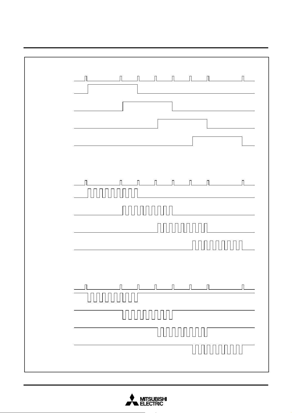
TIMING DIAGRAM
X
IN
RDE, WEL, WEH
Port P4 output
Port P4 input
Port P5 output
Port P5 input
Port P6 output
Port P6 input
trt
f
t
c
t
su(P4D–RDE)
t
su(P5D–RDE)
t
su(P6D–RDE)
t
d(WE–P4Q)
t
h(RDE–P4D)
t
d(WE–P5Q)
t
h(RDE–P5D)
t
d(WE–P6Q)
t
h(RDE–P6D)
16-BIT CMOS MICROCOMPUTER
t
t
w(H)
w(L)
Port P7 output
Port P7 input
Port P8 output
Port P8 input
t
su(P7D–RDE)
t
su(P8D–RDE)
t
d(WE–P7Q)
t
h(RDE–P7D)
t
d(WE–P8Q)
t
h(RDE–P8D)
27
MITSUBISHI MICROCOMPUTERS
M37735S4LHP
New product
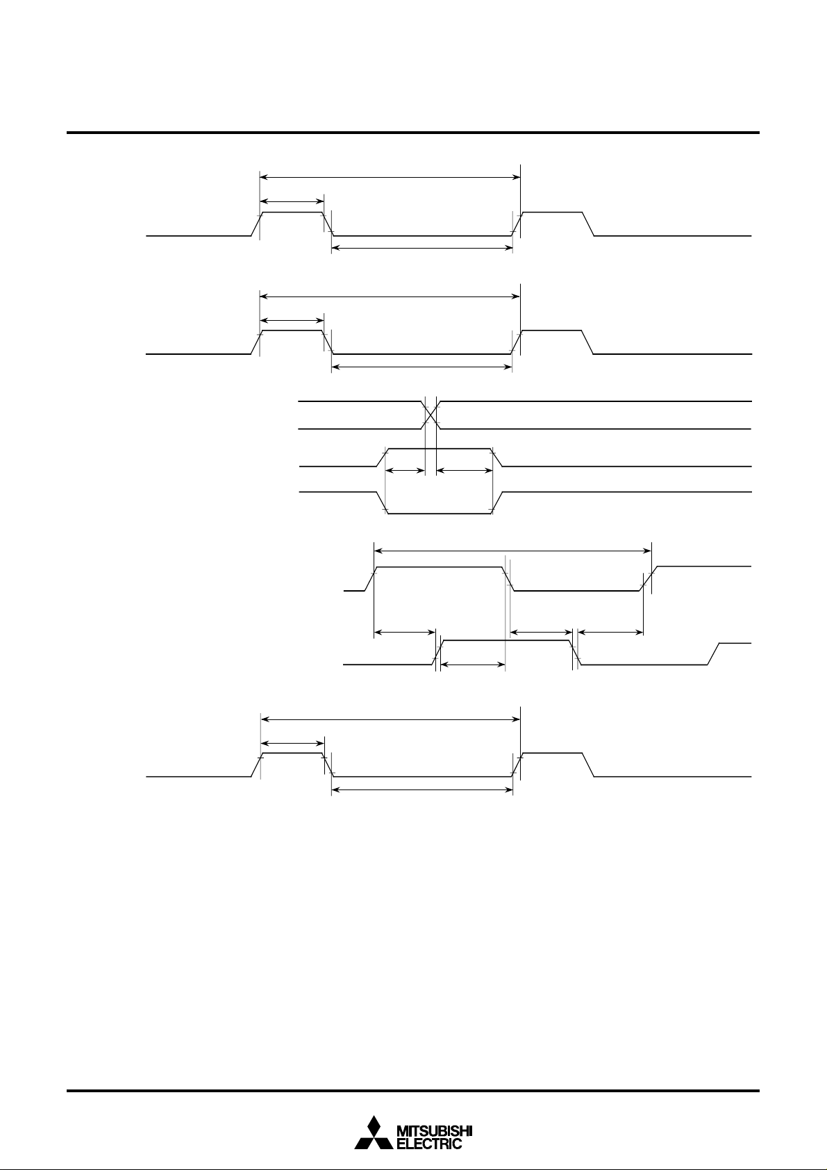
TAiIN input
OUT
input
TAi
In event count mode
t
w(TAH)
t
w(UPH)
TAi
OUT
input
(Up-down input)
IN
input
TAi
(when count by falling)
IN
input
TAi
(when count by rising)
t
c(TA)
t
w(TAL)
t
c(UP)
t
w(UPL)
t
h(TIN–UP)tsu(UP–TIN)
16-BIT CMOS MICROCOMPUTER
In event counter mode
(When two-phase pulse input is selected)
TAj
IN
input
OUT
input
TAj
TBiIN input
t
w(TBH)
t
su(TAjIN–TAjOUT)
t
c(TB)
t
w(TBL)
t
su(TAjOUT–TAjIN)
t
c(TA)
t
su(TAjIN–TAjOUT)
t
su(TAjOUT–TAjIN)
28

MITSUBISHI MICROCOMPUTERS
M37735S4LHP
New product
AD
TRG
input
CLK
i
TxD
i
RxD
i
t
w(ADL)
t
w(CKH)
t
w(INL)
t
d(C–Q)
t
c(AD)
t
c(CK)
t
w(CKL)
t
su(D–C)
16-BIT CMOS MICROCOMPUTER
t
h(C–Q)
t
h(C–D)
INTi
Kli
input
input
t
w(KNL)
t
w(INH)
29

MITSUBISHI MICROCOMPUTERS
M37735S4LHP
New product
Microprocessor mode
(When wait bit = “1”)
1
WEL
WEH
RDE
RDY
input
(When wait bit = “0”)
1
t
su(RDY–1)th(1–RDY)
16-BIT CMOS MICROCOMPUTER
WEL
WEH
RDE
RDY
input
(When wait bit = “1” or “0” in common)
1
t
su(HOLD–1)
HOLD
input
HLDA
output
t
d(1–HLDA)
t
su(RDY–1)th(1–RDY)
t
h(1–HOLD)
t
d(1–HLDA)
30
Test conditions
• V
CC
= 2.7 – 5.5 V
• Input timing voltage : V
• Output timing voltage : V
IL
= 0.2VCC, VIH = 0.8V
OL =
0.8 V, VOH = 2.0 V
CC

MITSUBISHI MICROCOMPUTERS
M37735S4LHP
New product
Microprocessor mode
(No wait : When wait bit = “1”)
t
w(L)
IN
X
1
CS
0
–
CS
4
An
t
d(CS–WE)
t
d(An–WE)
t
w(ALE)
t
w(H)
t
d(WE–1)
tft
Address
t
d(ALE–WE)
r
t
d(WE–1)
t
h(WE–An)
t
c
t
h(WE–CS)
t
t
d(CS–RDE)
t
d(An–RDE)
16-BIT CMOS MICROCOMPUTER
t
d(RDE–1)
Address Address
d(RDE–1)
t
h(RDE–CS)
t
h(RDE–An)
ALE
Am/Dm
WEL, WEH
Dm
IN
RDE
RSMP
t
t
su(A–ALE)
t
h(ALE–A)
t
h(WE–DQ)
d(ALE–RDE)
t
pxz(RDE–DZ)
t
pzx(RDE–DZ)
Address Data Address Address
t
d(A–RDE)
t
su(D–RDE)
t
h(RDE–D)
t
d(A–WE)
t
w(WE)
t
d(WE–DQ)
Data
t
w(RDE)
t
h(1–RSMP)
t
t
d(RSMP–WE)
d(RSMP–RDE)
Test conditions
• Vcc = 2.7 – 5.5 V
• Output timing voltage : VOL = 0.8 V, VOL = 2.0 V
• Data input Dm
IN
: VIL = 0.16 VCC, VIH = 0.5 VCC
31

MITSUBISHI MICROCOMPUTERS
M37735S4LHP
New product
Microprocessor mode
(Wait 1 : The external area is accessed when wait bit = “0” and wait selection bit = “1”.)
X
IN
1
CS0 – CS4
An
ALE
tw(L) tw(H) tf tr
td(WE– 1) td(RDE– 1)
td(CS–WE)
td(An–WE)
tw(ALE)
tc
td(WE– 1)
td(RDE- 1)
th(WE–CS)
Address Address
td(ALE–WE)
th(WE-An)
td(CS–RDE)
td(An–RDE)
16-BIT CMOS MICROCOMPUTER
th(RDE–CS)
th(RDE–An)
Am/Dm
WEL, WEH
DmIN
RDE
RSMP
tsu(A–ALE)
td(A–WE)
Address
td(RSMP–WE)
th(ALE–A)
td(WE–DQ)
tw(WE)
th( 1–RSMP)
td(ALE–RDE)
th(WE–DQ)
Data Address
td(A–RDE)
tpxz(RDE–DZ)
Address
tsu(D–RDE)
Data
tw(RDE)
td(RSMP–RDE)
tpzx(RDE–DZ)
th(RDE–D)
32
Test conditions
• Vcc = 2.7 – 5.5 V
• Output timing voltage : VOL = 0.8 V, VOH = 2.0 V
• Data input DmIN : VIL = 0.16 VCC, VIH = 0.5 VCC

MITSUBISHI MICROCOMPUTERS
M37735S4LHP
New product
Microprocessor mode
(Wait 0 : The external memory area is accessed when wait bit = “0” and wait selection bit = “0”.)
t
X
IN
CS
An
ALE
w(L)tw(H)tf
1
0
–
CS
4
r
t
d(WE–1)
t
d(CS–WE)
t
d(An–WE)
t
w(ALE)
tct
t
t
d(WE–1)
t
h(WE–CS)
d(RDE–1)
t
d(CS–RDE)
Address Address Address
t
d(An–RDE)
t
t
d(ALE–WE)
h(WE–An)
t
d(ALE–RDE)
16-BIT CMOS MICROCOMPUTER
t
d(RDE–1)
t
h(RDE–CS)
t
h(RDE–An)
Am/Dm
WEL, WEH
Dm
IN
RDE
RSMP
t
su(A–ALE)
t
Test conditions
• Vcc = 2.7 – 5.5 V
• Output timing voltage : V
IN
• Data input Dm
: VIL = 0.16 VCC, VIH = 0.5 VCC
t
d(A–WE)
d(RSMP–WE)
OL
= 0.8 V, VOH = 2.0 V
t
h(ALE–A)
t
d(WE–DQ)
t
w(WE)
t
h(1–RSMP)
t
h(WE–DQ)
t
d(RSMP–RDE)
AddressDataAddress
t
d(A–RDE)
t
pxz(RDE–DZ)
t
su(D–RDE)
t
w(RDE)
Data
t
pzx(RDE–DZ)
t
h(RDE–D)
Address
33

MITSUBISHI MICROCOMPUTERS
M37735S4LHP
New product
PACKAGE OUTLINE
16-BIT CMOS MICROCOMPUTER
34

New product
New product
MEMO
MITSUBISHI MICROCOMPUTERS
M37735S4LHP
16-BIT CMOS MICROCOMPUTER
35

MITSUBISHI MICROCOMPUTERS
M37735S4LHP
New product
16-BIT CMOS MICROCOMPUTER
Keep safety first in your circuit designs!
• Mitsubishi Electric Corporation puts the maximum effort into making semiconductor products better and more reliable, but there is always the possibility that trouble may occur with them. Trouble with
semiconductors may lead to personal injury, fire or property damage. Remember to give due consideration to safety when making your circuit designs, with appropriate measures such as (i) placement of
substitutive, auxiliary circuits, (ii) use of non-flammable material or (iii) prevention against any malfunction or mishap.
Notes regarding these materials
• These materials are intended as a reference to assist our customers in the selection of the Mitsubishi semiconductor product best suited to the customer’s application; they do not convey any license under any
intellectual property rights, or any other rights, belonging to Mitsubishi Electric Corporation or a third party.
• Mitsubishi Electric Corporation assumes no responsibility for any damage, or infringement of any third-party’s rights, originating in the use of any product data, diagrams, charts or circuit application examples
contained in these materials.
• All information contained in these materials, including product data, diagrams and charts, represent information on products at the time of publication of these materials, and are subject to change by Mitsubishi
Electric Corporation without notice due to product improvements or other reasons. It is therefore recommended that customers contact Mitsubishi Electric Corporation or an authorized Mitsubishi Semiconductor
product distributor for the latest product information before purchasing a product listed herein.
• Mitsubishi Electric Corporation semiconductors are not designed or manufactured for use in a device or system that is used under circumstances in which human life is potentially at stake. Please contact
Mitsubishi Electric Corporation or an authorized Mitsubishi Semiconductor product distributor when considering the use of a product contained herein for any specific purposes, such as apparatus or systems for
transportation, vehicular, medical, aerospace, nuclear, or undersea repeater use.
• The prior written approval of Mitsubishi Electric Corporation is necessary to reprint or reproduce in whole or in part these materials.
• If these products or technologies are subject to the Japanese export control restrictions, they must be exported under a license from the Japanese government and cannot be imported into a country other than the
approved destination.
Any diversion or reexport contrary to the export control laws and regulations of Japan and/or the country of destination is prohibited.
• Please contact Mitsubishi Electric Corporation or an authorized Mitsubishi Semiconductor product distributor for further details on these materials or the products contained therein.
© 1996 MITSUBISHI ELECTRIC CORP.
H-LF430-A KI-9606 Printed in Japan (ROD)
New publication, effective Jun. 1996.
Specifications subject to change without notice.
 Loading...