MITSUBISHI MICROCOMPUTERS
M37735S4BFP
PRELIMINARY
Notice: This is not a final specification.
Some parametric limits are subject to change.
16-BIT CMOS MICROCOMPUTER
DESCRIPTION
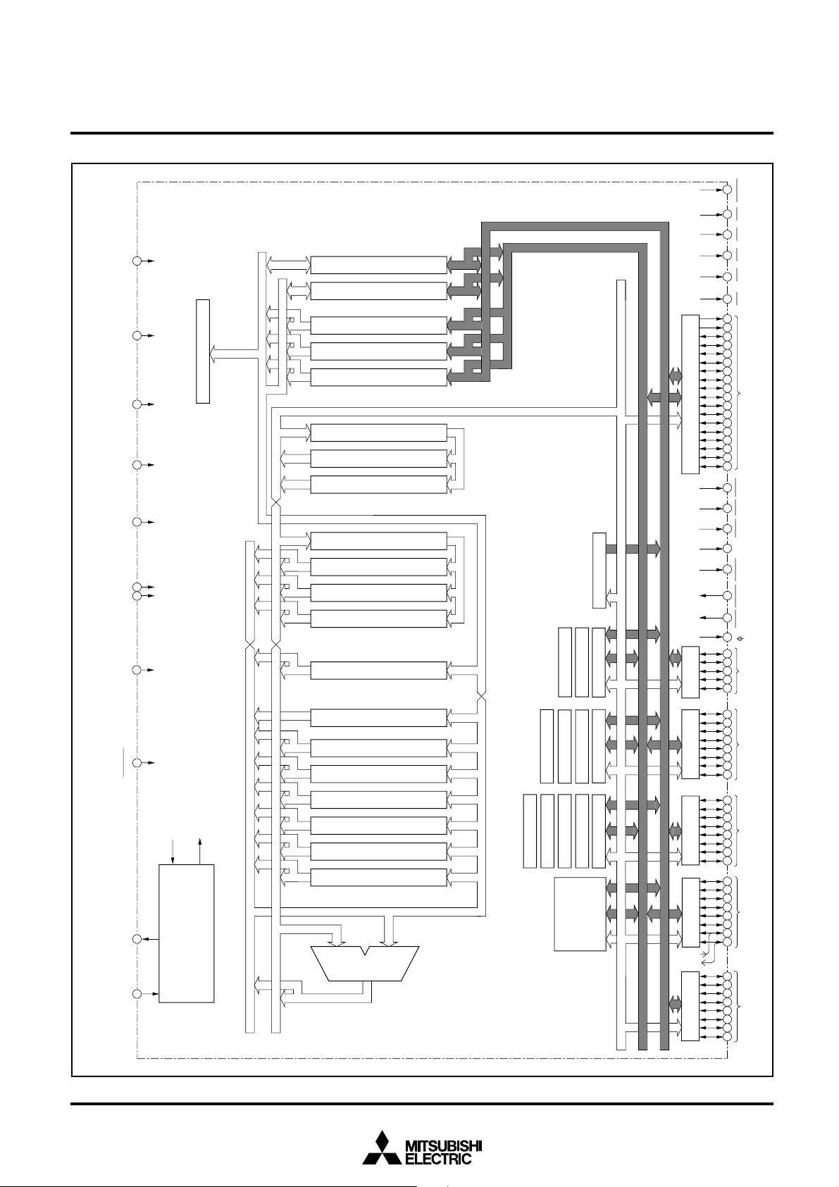
The M37735S4BFP is a microcomputer using the 7700 Family core.
This microcomputer has a CPU and a bus interface unit. The CPU is
a 16-bit parallel processor that can be an 8-bit parallel processor,
and the bus interface unit enhances the memory access efficiency to
execute instructions fast. This microcomputer also includes a 32 kHz
oscillation circuit, in addition to the RAM, multiple-function timers,
serial I/O, A-D converter, and so on.
FEATURES
●Number of basic instructions .................................................. 103
●Memory size RAM ................................................ 2048 bytes
●Instruction execution time
The fastest instruction at 25 MHz frequency ...................... 160 ns
●Single power supply ...................................................... 5 V ± 10%
●Low power dissipation (at 25 MHz frequency)
............................................ 47.5 mW (Typ.)
●Interrupts ............................................................ 19 types, 7 levels
●Multiple-function 16-bit timer ................................................. 5 + 3
●Serial I/O (UART or clock synchronous)..........................................3
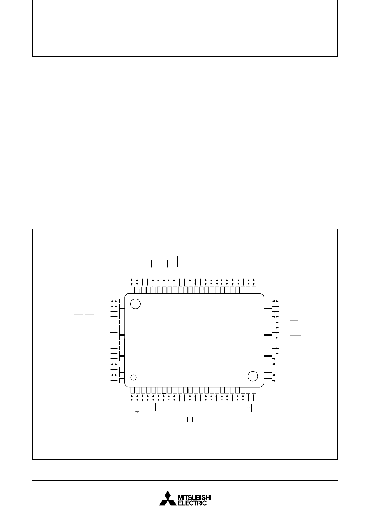
PIN CONFIGURATION (TOP VIEW)
1
RTS
/
1
1
1
CTS
/
4
P8
/CLK
5
P8
D
X
/R
6
P8
1
D
X
/T
7
P8
0
CS
/
0
P0
1
CS
/
1
P0
2
CS
/
2
P0
3
CS
/
3
P0
●10-bit A-D converter ..............................................8-channel inputs
●12-bit watchdog timer
●Programmable input/output
(ports P4, P5, P6, P7, P8) ..............................................................37
●Clock generating circuit ........................................ 2 circuits built-in
APPLICATION
Control devices for general commercial equipment such as office
automation, office equipment, and so on.
Control devices for general industrial equipment such as
communication equipment, and so on.
4
CS
/
4
P0
16
RSMP
/
/A
6
5
P0
P0
17
/A
7
P0
8
/D
8
/A
0
P1
9
/D
9
/A
1
P1
10
/D
10
/A
2
P1
11
/D
11
/A
3
P1
12
/D
12
/A
4
P1
13
/D
13
/A
5
P1
14
/D
14
/A
6
P1
15
/D
15
/A
7
P1
0
/D
0
/A
0
P2
1
/D
1
/A
1
P2
2
/D
2
/A
2
P2
3
/D
3
/A
3
P2
P82/RXD0/CLKS
P8
0
/CTS0/RTS0/
P76/AN6/Xc
P75/AN5/
P74/AN4/RXD
P73/AN3/CLK
P72/AN2/
P83/TXD
P81/CLK
CLKS
AV
V
AV
P77/AN7/Xc
AD
TRG
/TXD
CTS
P71/AN
V
REF
V
OUT
CC
CC
SS
SS
61
4
IN
/TB0
5
P6
2
NT
/I
4
P6
58
56
59
57
60
55
M37735S4BFP
1
NT
/I
3
P6
9
7
0
NT
/I
2
P6
8
IN
/TA4
1
P6
OUT
/TA4
0
P6
10
3
/RTP1
3
KI
/
IN
/TA3
7
6
5
64
62
63
65
0
66
0
67
0
68
1
69
70
71
72
73
74
IN
75
76
2
77
2
78
2
79
2
80
1
1
2
3
0
IN
SUB
/AN
0
/
/TB1
6
IN
P7
P6
/TB2
7
P6
P5
54
53
12
11
1
2
/RTP1
/RTP1
1
2
KI
KI
/
/
IN
OUT
/TA2
5
/TA3
6
P5
P5
51
52
14
13
3
0
/RTP0
/RTP1
0
IN
KI
/
/TA1
OUT
3
P5
/TA2
4
P5
49
50
16
15
2
1
/RTP0
/RTP0
IN
OUT
/TA0
1
/TA1
2
P5
P5
47
48
18
17
0
7
P4
/RTP0
OUT
/TA0
0
P5
46
19
6
P4
42
41
43
44
45
40
P24/A4/D
P25/A5/D
P26/A6/D
P27/A7/D
P30/
WEL
P31/
WEH
P32/
ALE
P33/
HLDA
V
ss
RDE
X
OUT
X
IN
RESET
CNV
SS
BYTE
HOLD
4
5
6
7
39
38
37
36
35
34
33
32
31
30
29
28
27
26
25
21
22
4
P4
3
P4
24
23
1
/
RDY
2
20
5
P4
P4
Outline 80P6N-A
PRELIMINARY
X
IN
X
OUT
RESET
Reset input
V
REF
P8(8) P7(8) P5(8) P6(8) P4(5)
Address (18)/Data (16)
CNVss
BYTE
UART1(9)
UART0(9)
AV
SS
(0V)
AV
CC
(0V)
V
SS
V
CC
A-D Converter(10)
X
CIN
X
COUT
X
CIN
X
COUT
Clock input Clock output
Reference
voltage input
External data bus width
selection input
Clock Generating Circuit
Instruction Register(8)
Arithmetic Logic
Unit(16)
Accumulator A(16)
Accumulatcr B(16)
Index Register X(16)
Index Register Y(16)
Stack Pointer S(16)
Direct Page Register DPR(16)
Input Butter Register IB(16)
Data Bank Register DT(8)
Program Bank Register PG(8)
Incrementer/Decrementer(24)
Data Address Register DA(24)
Incrementer(24)
Instruction Queue Buffer Q
2
(8)
Instruction Queue Buffer Q
1
(8)
Instruction Queue Buffer Q
0
(8)
Data Buffer DB
L
(8)
Data Buffer DB
H
(8)
RAM
2048 bytes
Timer TA3(16)
Timer TA4(16)
Timer TA2(16)
Timer TA1(16)
Timer TA0(16)
Watchdog Timer
Timer TB2(16)
Timer TB1(16)
Timer TB0(16)
Address Bus
Data Bus(Odd)
Data Bus(Even)
Input/Output
port P8
Input/Output
port P7
Input/Output
port P6
Input/Output
port P5
Input/Output
port P4
Address bus/Data bus
UART2(9 )
WEL
WEHALEHLDAHOLDRDY
1
RDE
RSMP
CS
0
CS
1
CS
2
CS
3
CS
4
Processor Status Register PS(11)
Program Counter PC(16)
Program Address Register PA(24)
Notice: This is not a final specification.
Some parametric limits are subject to change.
MITSUBISHI MICROCOMPUTERS
M37735S4BFP
16-BIT CMOS MICROCOMPUTER
M37735S4BFP BLOCK DIAGRAM
2
MITSUBISHI MICROCOMPUTERS
M37735S4BFP
PRELIMINARY
Notice: This is not a final specification.
Some parametric limits are subject to change.
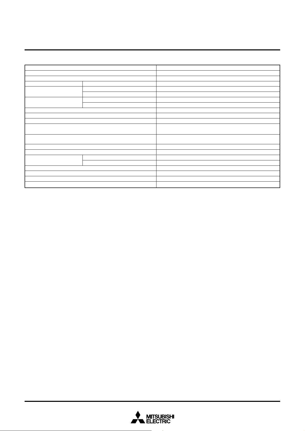
FUNCTIONS OF M37735S4BFP
Parameter Functions
Number of basic instructions 103
Instruction execution time 160ns (the fastest instruction at external clock 25 MHz frequency)
Memory size RAM 2048 bytes
Input/Output ports
Multi-function timers
Serial I/O (UART or clock synchronous serial I/O) ✕ 3
A-D converter 10-bit ✕ 1 (8 channels)
Watchdog timer 12-bit ✕ 1
Interrupts
Clock generating circuit
Supply voltage 5 V ± 10%
Power dissipation
Input/Output characteristic
Memory expansion Maximum 1 Mbytes
Operating temperature range –20 to 85 °C
Device structure CMOS high-performance silicon gate process
Package 80-pin plastic molded QFP (80P6N-A)
P5 – P8 8-bit ✕ 4
P4 5-bit ✕ 1
TA0, TA1, TA2, TA3, TA4 16-bit ✕ 5
TB0, TB1, TB2 16-bit ✕ 3
3 external types, 16 internal types
Each interrupt can be set to the priority level (0 – 7.)
2 circuits built-in (externally connected to a ceramic resonator or a
quartz-crystal oscillator)
47.5 mW (at external clock 25 MHz frequency)
Input/Output voltage 5 V
Output current 5 mA
16-BIT CMOS MICROCOMPUTER
3

MITSUBISHI MICROCOMPUTERS
M37735S4BFP
PRELIMINARY
Notice: This is not a final specification.
Some parametric limits are subject to change.
PIN DESCRIPTION
Pin Name Input/Output Functions
Vcc, Power source Apply 5 V ± 10% to Vcc and 0 V to Vss.
Vss
CNVss CNVss input Input Connect to Vcc.
_____
RESET Reset input Input When “L” level is applied to this pin, the microcomputer enters the reset state.
XIN Clock input Input
XOUT Clock output Output
____
RDE
BYTE
Read enable output
Bus width
Output
Input This pin determines whether the external data bus has an 8-bit width or a 16-bit width.
selection input The data bus has a 16-bit width when “L” signal is input and an 8-bit width when “H” signal
AVcc, Analog power Power source input pin for the A-D converter. Externally connect AVcc to Vcc and AVss to Vss.
AVss source input
V
REF Reference Input This is reference voltage input pin for the A-D converter.
voltage input
____
P00/CS0 – Chip selection Output
____
P04/CS4 output
_____
P05/RSMP
Ready sampling
Output
output
P06/A16,
Address output
Output An address (A16, A17) is output.
P07/A17
P10/A8/D8 – Address output
P17/A15/D15/data
(high
I/O When the BYTE pin is set
-order) I/O
P20/A0/D0 –
P27/A7/D7
P30/WEL Write enable Output
____
Address output
/data (low
-order) I/O
I/O Low-order data (D0 – D7) is input/output or an address (A0 – A7) is output.
output is “L”. When the BYTE pin is “H” and writing to an even address or an odd address is performed,
____
P31/WEH Write enable Output
high output
P3
2/ALE Address latch Output This is used to retrieve only the address from the multiplex signal which consists of address and
enable output data.
_____
P33/HLDA Hold acknow- Output This outputs “L” level when the microcomputer enters hold state after a hold request is accepted.
_____
HOLD Hold request Input
____
RDY Ready input Input
ledge output
input signal is “L”.
These are pins of main-clock generating circuit. Connect a ceramic resonator or a quartz-crystal
oscillator between X
IN and XOUT. When an external clock is used, the clock source should be
connected to the XIN pin, and the XOUT pin should be left open.
When data/instruction read is performed, output level of RDE signal is “L”.
is input.
When the specified external memory area is accessed, CS0 – CS4 signals are “L”.
The timing signal to be input to the RDY pin is output.
to
____
“L”
and
external data bus has a 16-bit width, high-order data
(D8 – D15) is input/output or an address (A8 – A15) is output. When the BYTE pin is “H” and an
external data bus has an 8-bit width, only address (A8 – A15) is output.
When the BYTE pin is “L” and writing to an even address is performed, output level of WEL signal
output level of WEL signal is “L”.
When the BYTE pin is “L” and writing to an odd address is performed, output level of WEH signal
is “L”. When the BYTE pin is “H”, WEH signal is always “H”.
This is an input pin for HOLD request signal. The microcomputer enters hold state while this
This is an input pin for RDY signal. The microcomputer enters ready state while this signal is “L”.
____
____
_____
____
16-BIT CMOS MICROCOMPUTER
____
____ ____
____
____
P42/ 1 Clock output Output This pin outputs the clock 1.
P4
3 – P47 I/O port P4 I/O These pins become a 5-bit I/O port. An I/O direction register is available so that each pin can be
programmed for input or output. These ports are in the input mode when reset.
P5
0 – P57 I/O port P5 I/O In addition to having the same functions as port P4, these pins also function as I/O pins for timers
A0 to A3 and input pins for key input interrupt input (KI0 – KI3).
P6
0 – P67 I/O port P6 I/O In addition to having the same functions as port P4, these pins also function as I/O pins for timer
A4, input pins for external interrupt input (INT0 – INT2) and input pins for timers B0 to B2. P67 also
____ ____
___ ___
functions as sub-clock SUB output pin.
P7
0 – P77 I/O port P7 I/O In addition to having the same functions as port P4, these pins function as input pins for A-D
converter. P72 to P75 also function as I/O pins for UART2. Additionally, P76 and P77 have the
function as the output pin (XCOUT) and the input pin (XCIN) of the sub-clock (32 kHz) oscillation
circuit, respectively. When P76 and P77 are used as the XCOUT and XCIN pins, connect a resonator
or an oscillator between the both.
P80 – P87 I/O port P8 I/O In addition to having the same functions as port P4, these pins also function as I/O pins for UART
0 and UART 1.
4
PRELIMINARY
Notice: This is not a final specification.
Some parametric limits are subject to change.
MITSUBISHI MICROCOMPUTERS
M37735S4BFP
16-BIT CMOS MICROCOMPUTER
BASIC FUNCTION BLOCKS
The M37735S4BFP has the same functions as the
M37735MHBXXXFP except for the following:
(1) The memory map is different.
(2) The processor mode is different.
(3) The reset circuit is different.
(4) Pulse output port mode of timer A is available.
(5) The function of ROM area modification is not available.
Refer to the section on the M37735MHBXXXFP, except for above
(1)–(5).
MEMORY
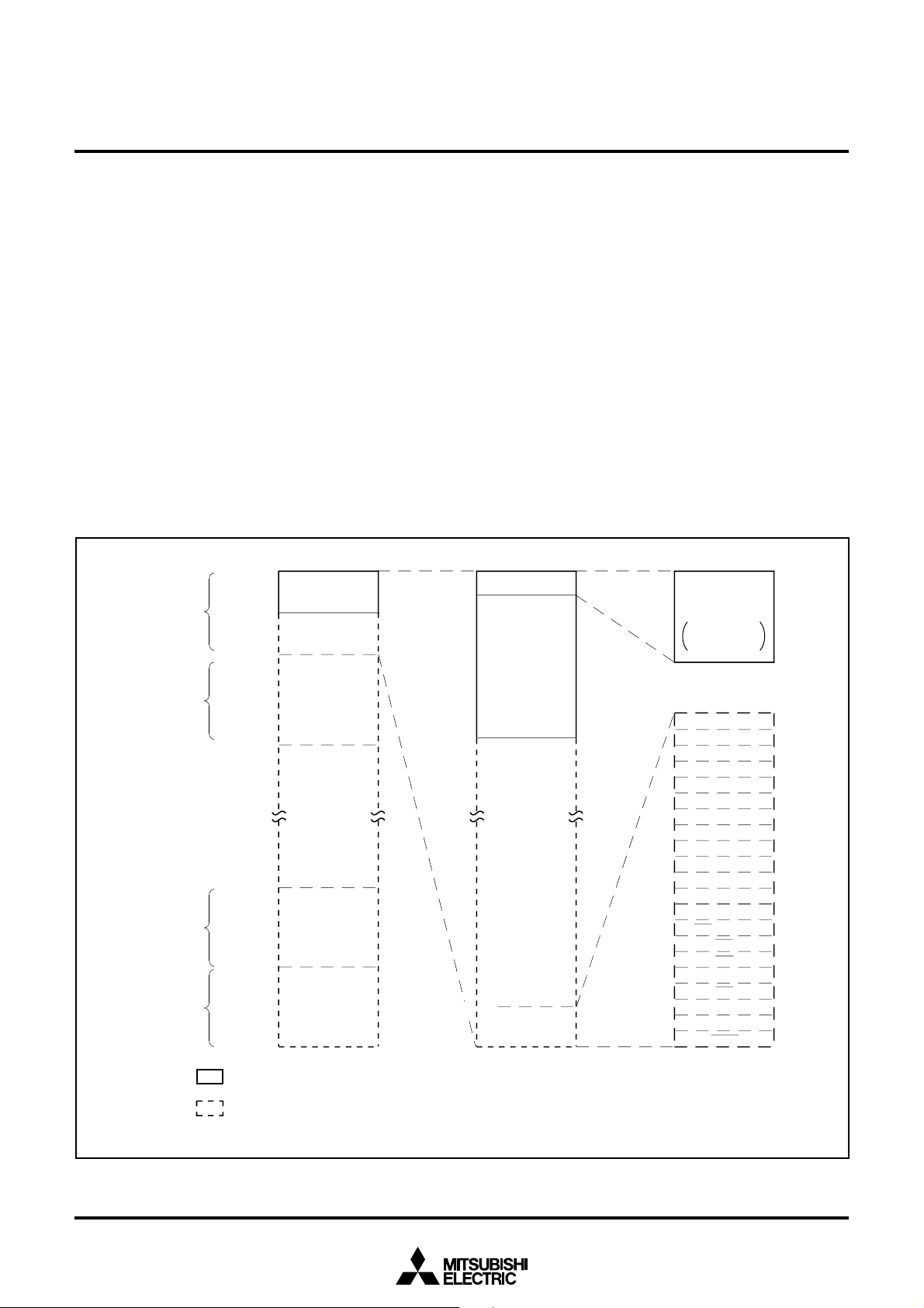
The memory map is shown in Figure 1. The address space has a
capacity of 16 Mbytes and is allocated to addresses from 0
FFFFFF
16. The address space is divided by 64-Kbyte unit called bank.
The banks are numbered from 0
However, banks 10
16–FF16 of the M37735S4BFP cannot be
16 to FF16.
accessed.
000000
16
Bank 0
16
00FFFF
16
010000
16
16 to
000000
00007F
000080
Built-in RAM and control registers for internal peripheral devices are
assigned to bank 0
Addresses FFD6
16.
16 to FFFF16 are the RESET and interrupt vector
addresses and contain the interrupt vectors. Use ROM for memory
of this address.
The 2048-byte area allocated to addresses from 80
16 to 87F16 is the
built-in RAM. In addition to storing data, the RAM is used as stack
during a subroutine call or interrupts.
Peripheral devices such as I/O ports, A-D converter, serial I/O, timer,
and interrupt control registers are allocated to addresses from 0
7F
16.
A 256-byte direct page area can be allocated anywhere in bank 0
by using the direct page register (DPR). In the direct page addressing
mode, the memory in the direct page area can be accessed with two
words. Hence program steps can be reduced.
16
16
16
Internal RAM
2048 bytes
000000
00007F
16
Internal peripheral
devices
control registers
refer to Fig. 2 for
detail information
16
16 to
16
Bank 1
16
• • • • • • • • • • • • • • • • • • •
Bank FE
16
Bank FF
16
00087F
00FFD6
00FFFF
16
16
16
01FFFF
FE0000
FEFFFF
FF0000
FFFFFF
16
16
16
16
16
: Internal
: External
Note. Banks 1016–FF16 cannot be accessed in the M37735S4BFP.
00FFD6
00FFFE
Interrupt vector table
16
A-D/UART2 trans./rece.
UART1 transmission
UART1 receive
UART0 transmission
UART0 receive
Timer B2
Timer B1
Timer B0
Timer A4
Timer A3
Timer A2
Timer A1
Timer A0
INT
2
/Key input
INT
1
INT
0
Watchdog timer
DBC
BRK instruction
Zero divide
16
RESET
Fig. 1 Memory map
5
PRELIMINARY
Notice: This is not a final specification.
Some parametric limits are subject to change.
MITSUBISHI MICROCOMPUTERS
M37735S4BFP
16-BIT CMOS MICROCOMPUTER
Address (Hexadecimal notation)
000000
000001
000002
000003
000004
000005
000006
000007
000008
000009
00000A
00000B
00000C
00000D
00000E
00000F
000010
000011
000012
Port P0 register
Port P1 register
Port P0 direction register
Port P1 direction register
Port P2 register
Port P3 register
Port P2 direction register
Port P3 direction register
Port P4 register
Port P5 register
Port P4 direction register
Port P5 direction register
Port P6 register
Port P7 register
Port P6 direction register
Port P7 direction register
Port P8 register
000013
000014
Port P8 direction register
000015
000016
000017
000018
000019
00001A
00001B
00001C
00001D
00001E
00001F
000020
000021
000022
000023
000024
000025
000026
000027
000028
000029
00002A
00002B
00002C
00002D
00002E
00002F
000030
000031
000032
000033
000034
000035
000036
000037
000038
000039
00003A
00003B
00003C
00003D
00003E
00003F
Pulse output data register 1
Pulse output data register 0
A-D control register 0
A-D control register 1
A-D register 0
A-D register 1
A-D register 2
A-D register 3
A-D register 4
A-D register 5
A-D register 6
A-D register 7
UART 0 transmit/receive mode register
UART 0 baud rate register (BRG0)
UART 0 transmission buffer register
UART 0 transmit/receive control register 0
UART 0 transmit/receive control register 1
UART 0 receive buffer register
UART 1 transmit/receive mode register
UART 1 baud rate register (BRG1)
UART 1 transmission buffer register
UART 1 transmit/receive control register 0
UART 1 transmit/receive control register 1
UART 1 receive buffer register
Address (Hexadecimal notation)
000040
Count start flag
000041
000042
One-shot start flag
000043
000044
Up-down flag
000045
000046
000047
000048
000049
00004A
00004B
00004C
00004D
00004E
00004F
000050
000051
000052
000053
000054
000055
000056
000057
000058
000059
00005A
00005B
00005C
00005D
00005E
00005F
000060
000061
000062
000063
000064
000065
000066
000067
000068
000069
00006A
00006B
00006C
00006D
00006E
00006F
000070
000071
000072
000073
000074
000075
000076
000077
000078
000079
00007A
00007B
00007C
00007D
00007E
00007F
Timer A0 register
Timer A1 register
Timer A2 register
Timer A3 register
Timer A4 register
Timer B0 register
Timer B1 register
Timer B2 register
Timer A0 mode register
Timer A1 mode register
Timer A2 mode register
Timer A3 mode register
Timer A4 mode register
Timer B0 mode register
Timer B1 mode register
Timer B2 mode register
Processor mode register 0
Processor mode register 1
Watchdog timer register
Watchdog timer frequency selection flag
Waveform output mode register
Reserved area (Note)
UART2 transmit/receive mode register
UART2 baud rate register (BRG2)
UART2 transmission buffer register
UART2 transmit/receive control register 0
UART2 transmit/receive control register 1
UART2 receive buffer register
Oscillation circuit control register 0
Port function control register
Serial transmit control register
Oscillation circuit control register 1
A-D/UART2 trans./rece. interrupt control register
UART 0 transmission interrupt control register
UART 0 receive interrupt control register
UART 1 transmission interrupt control register
UART 1 receive interrupt control register
Timer A0 interrupt control register
Timer A1 interrupt control register
Timer A2 interrupt control register
Timer A3 interrupt control register
Timer A4 interrupt control register
Timer B0 interrupt control register
Timer B1 interrupt control register
Timer B2 interrupt control register
INT
0
interrupt control register
INT
1
interrupt control register
INT
2
/Key input interrupt control register
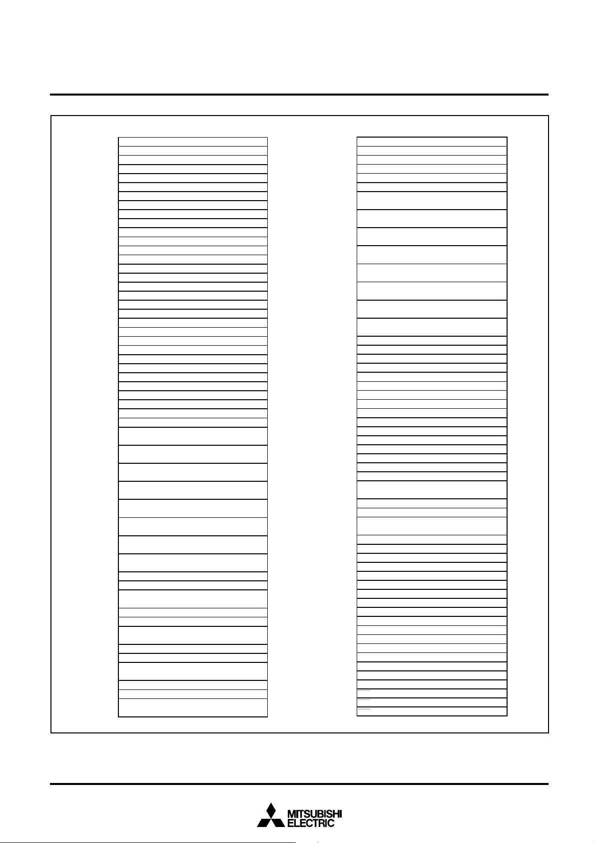
Note. Writing to reserved area is disabled.
Fig. 2 Location of internal peripheral devices and interrupt control registers
6
PRELIMINARY
Notice: This is not a final specification.
Some parametric limits are subject to change.
MITSUBISHI MICROCOMPUTERS
M37735S4BFP
16-BIT CMOS MICROCOMPUTER
Pulse output port mode
The pulse motor drive waveform can be output by using plural internal
timer A.
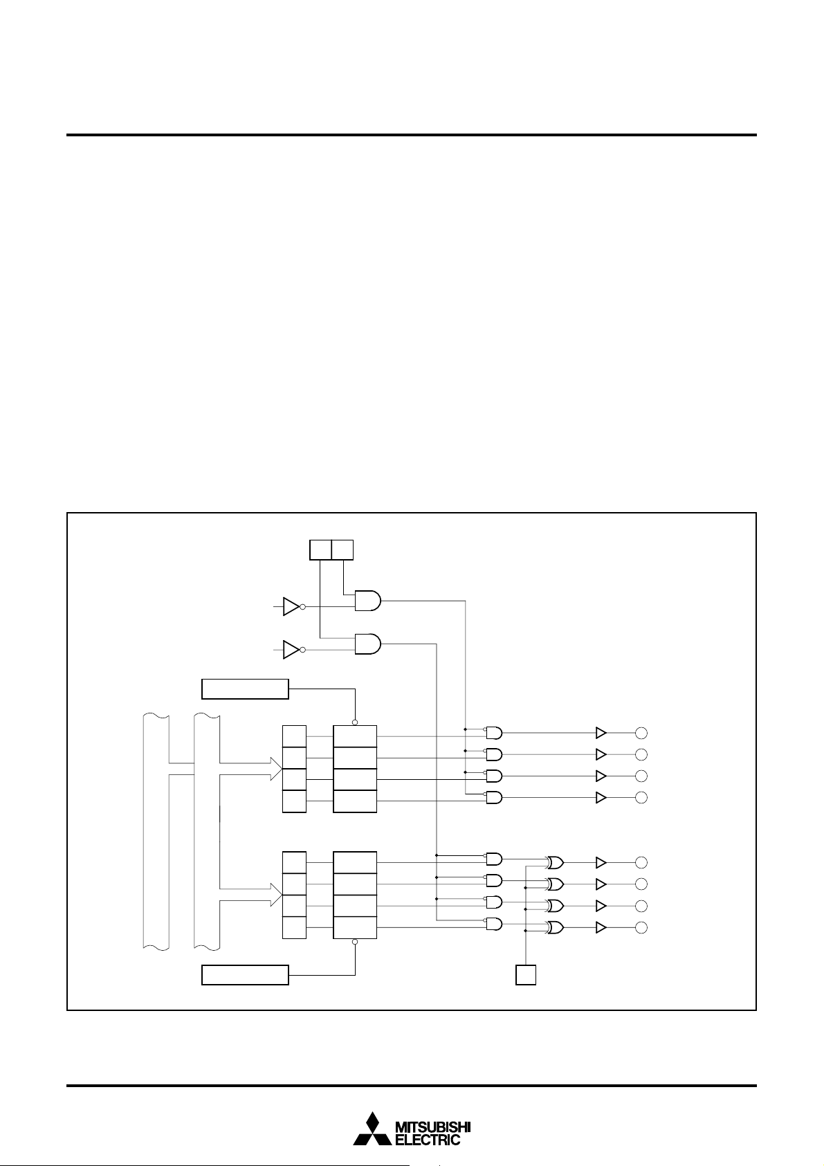
Figure 3 shows a block diagram for pulse output port mode. In the
pulse output port mode, two pairs of four-bit pulse output ports are
used. Whether using pulse output port or not can be selected by
waveform output selection bit (bit 0, bit 1) of waveform output mode
register (62
output selection bit is set to “1”, RTP1
are used as pulse output ports, and when bit 1 of waveform output
selection bit is set to “1”, RTP0
used as pulse output ports. When bits 1 and 0 of waveform output
selection bit are set to“1”, RTP1
RTP0
The ports not used as pulse output ports can be used as normal
parallel ports, timer input/output or key input interruput input.
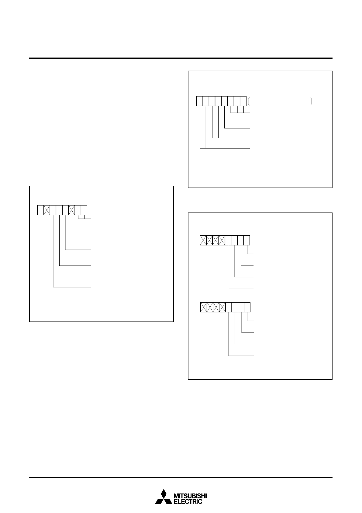
In the pulse output port mode, set timers A0 and A2 to timer mode as
timers A0 and A2 are used. Figure 5 shows the bit configuration of
timer A0, A2 mode registers in pulse output port mode.
Data can be set in each bit of the pulse output data register
corresponding to four ports selected as pulse output ports. Figure 6
16 address) shown in Figure 4. When bit 0 of waveform
0, RTP11, RTP12, and RTP13
0, RTP01, RTP02, and RTP03 are
0, RTP11, RTP12, and RTP13, and
0, RTP01, RTP02, and RTP03 are used as pulse output ports.
Pulse width modulation selection bit
(Bit 4, 5 of 62
16 address)
45
shows the bit configuration of the pulse output data register. The
contents of the pulse output data register 1 (low-order four bits of
1C
16 address) corresponding to RTP10, RTP11, RTP12, and RTP13
is output to the ports each time the counter of timer A2 becomes
0000
16. The contents of the pulse output data register 0 (low-order
four bits of 1D
and RTP0
becomes 0000
16 address) corresponding to RTP00, RTP01, RTP02,
3 is output to the ports each time the counter of timer A0
16.
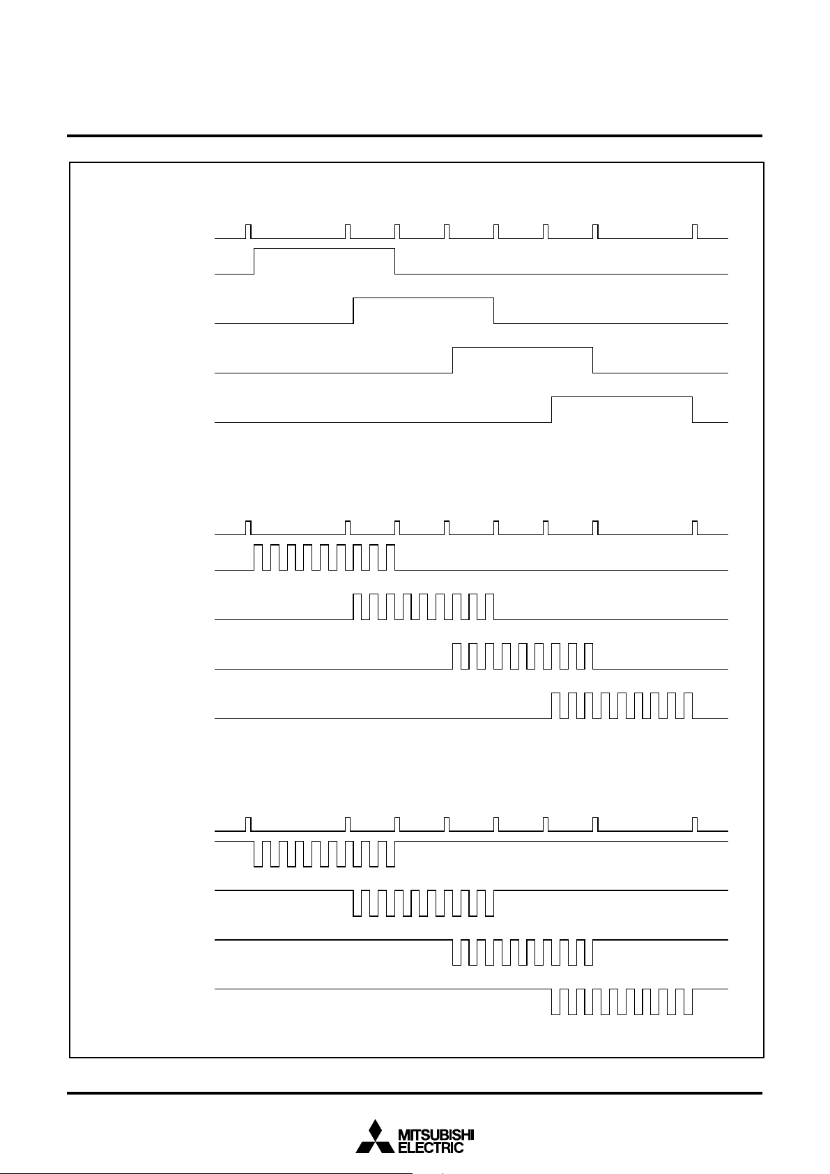
Figure 7 shows example of waveforms in pulse output port mode.
When “0” is written to a specified bit of the pulse output data register,“L”
level is output to the corresponding pulse output port when the counter
of corresponding timer becomes 0000
16, and when “1” is written, “H”
level is output to the pulse output port.
Pulse width modulation can be applied to each pulse output port.
Since pulse width modulation involves the use of timers A1 and A3,
activate these timers in pulse width modulation mode.
Pulse width modulation output
Pulse width modulation output
Data bus (even)
by timer A3
by timer A1
Timer A2
Pulse output data
register 1 (1C16 address)
Data bus (odd)
Pulse output data
register 0 (1D
Timer A0
3
D
D2
D1
D0
D11
D10
D9
D8
16 address)
D
D
D
D
D
D
D
D
T
Q
Q
Q
Q
Q
Q
Q
Q
T
Polarity selection bit
(Bit 3 of 62
16 address)
3 (P57)
RTP1
RTP1
2 (P56)
RTP1
1 (P55)
RTP1
0 (P54)
RTP0
3 (P53)
RTP02 (P52)
RTP0
1 (P51)
RTP0
0 (P50)
Fig. 3 Block diagram for pulse output port mode
7
PRELIMINARY
Notice: This is not a final specification.
Some parametric limits are subject to change.
RTP10, RTP11, RTP12, and RTP13 are applied pulse width modulation
by timer A3 by setting the pulse width modulation selection bit by
timer A3 (bit 5) of the waveform output mode register to “1”.
RTP0
0, RTP01, RTP02, and RTP03 are applied pulse width modulation
by timer A1 by setting the pulse width modulation selection bit by
timer A1 (bit 4) of the waveform output mode register to “1”.
The contents of the pulse output data register 0 can be reversed and
output to pulse output ports RTP0
the polarity selection bit (bit 3) of the waveform output mode register.
When the polarity selection bit is “0”, the contents of the pulse output
data register 0 is output unchangeably, and when “1”, the contents of
the pulse output data register 0 is reversed and output. When pulse
width modulation is applied, likewise the polarity reverse to pulse
width modulation can be selected by the polarity selection bit.
0, RTP01, RTP02, and RTP03 by
MITSUBISHI MICROCOMPUTERS
765432 01
0 0 X 1 0 0
M37735S4BFP
16-BIT CMOS MICROCOMPUTER
Address
Timer A0 mode register 5616
Timer A2 mode register 5816
Always “100” in pulse output
port mode
Not used in pulse output port mode
Always “00” in pulse output port mode
Clock source selection bit
0 0 : Select f
0 1 : Select f16
1 0 : Select f64
1 1 : Select f512
2
765432 01
0
Weveform output mode register 6216
Weveform output selection bit
0 0 : Parallel port
0 1 : RTP1 selected
1 0 : RTP0 selected
1 1 : RTP1 and RTP0 selected
Polarity selection bit
0 : Positive polarity
1 : Negative polarity
Pulse width modulation selection bit
by timer A1
0 : Not modulated
1 : Modulated
Pulse width modulation selection bit
by timer A3
0 : Not modulated
1 : Modulated
Always “0”
Fig. 4 Waveform output mode register bit configuration
Address
Fig. 5 Timer A0, A2 mode register bit configuration in pulse output
port mode
765432 01
Pulse output data register 0 1D16
RTP00 output data
RTP01 output data
RTP02 output data
RTP03 output data
765432 01
Pulse output data register 1 1C16
RTP10 output data
RTP11 output data
RTP12 output data
RTP13 output data
Address
Address
Fig. 6 Pulse output data register bit configuration
8
PRELIMINARY
Notice: This is not a final specification.
Some parametric limits are subject to change.
Output signal at each time
when timer A2 becomes 0000
3(P57)
RTP1
RTP1
2(P56)
1(P55)
RTP1
RTP10(P54)
16
MITSUBISHI MICROCOMPUTERS
M37735S4BFP
16-BIT CMOS MICROCOMPUTER
Example of pulse output port (RTP10 – RTP13)
Output signal at each time
when timer A2 becomes 0000
3(P57)
RTP1
RTP1
2(P56)
1(P55)
RTP1
0(P54)
RTP1
Output signal at each time
when timer A0 becomes 0000
RTP0
3(P53)
Example of pulse output port (RTP10 – RTP13) when pulse width modulation is applied by timer A3.
16
Example of pulse output port (RTP00 – RTP03) when pulse width modulation is applied
by timer A1 with polarity selection bit = “1”.
16
RTP0
2(P52)
1(P51)
RTP0
0(P50)
RTP0
Fig. 7 Example of waveforms in pulse output port mode
9
PRELIMINARY
Notice: This is not a final specification.
Some parametric limits are subject to change.
PROCESSOR MODE
Only the microprocessor mode can be selected.
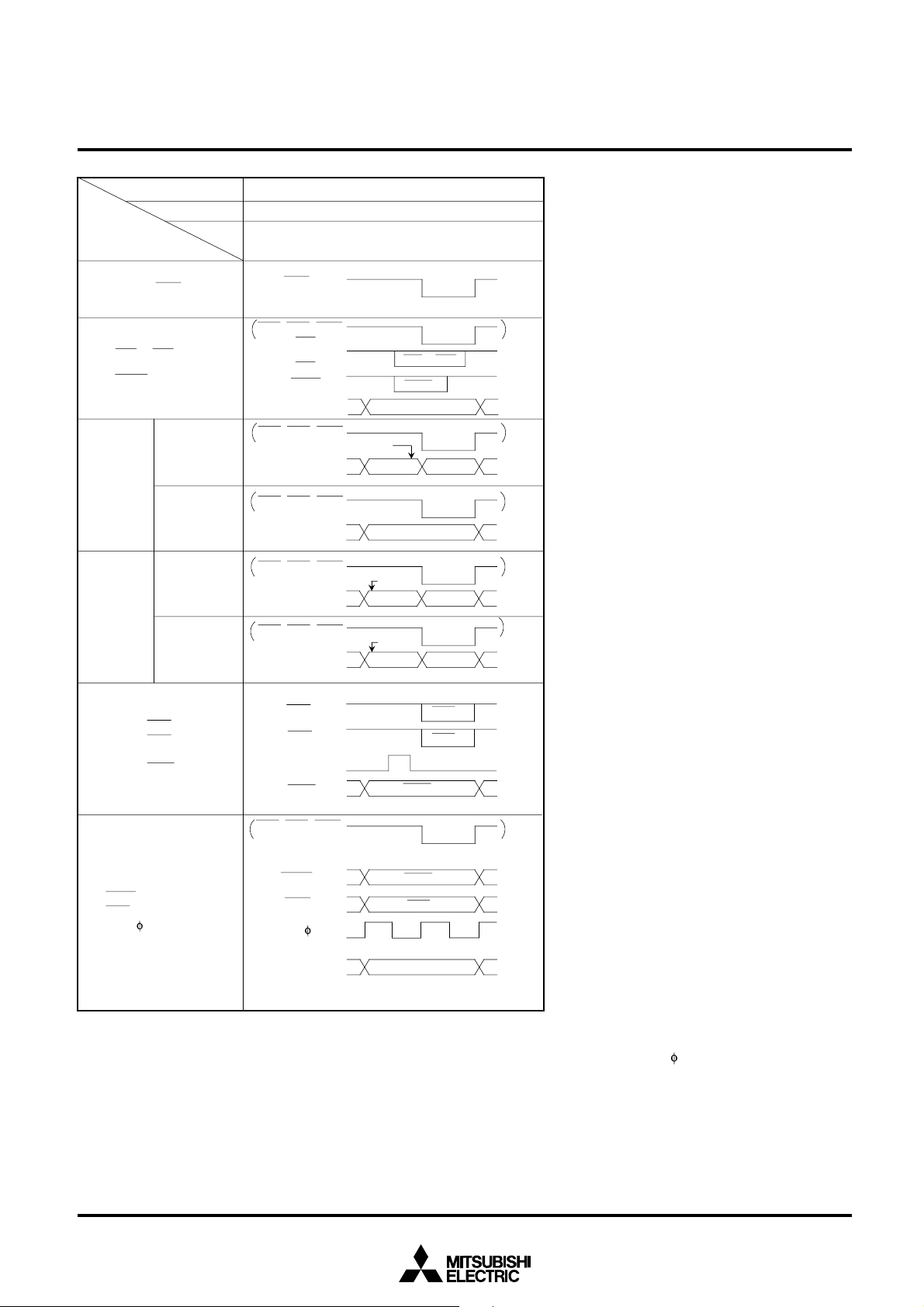
Figure 9 shows the functions of pins P00/CS0 — P47 in the
microprocessor mode.
Figure 10 shows external memory area for the microprocessor mode.
Access to the external memory is affected by the BYTE pin, the wait
bit (bit 2 of the processor mode register 0 at address 5E
wait selection bit (bit 0 of the processor mode register 1 at address
5F
16) .
___
16), and the
MITSUBISHI MICROCOMPUTERS
M37735S4BFP
16-BIT CMOS MICROCOMPUTER
• BYTE pin
When accessing the external memory, the level of the BYTE pin is
used to determine whether to use the data bus as 8-bit width or 16bit width.
The data bus has a width of 8 bits when level of the BYTE pin is “H”,
and pins P2
The data bus has a width of 16 bits when the level of the BYTE pin is
“L”, and pins P2
D
15 are the data I/O pins.
When accessing the internal memory, the data bus always has a
width of 16 bits regardless of the BYTE pin level.
0/A0/D0 — P27/A7/D7 are the data I/O pins.
0/A0/D0 — P27/A7/D7 and pins P10/A8/D8 — P17/A15/
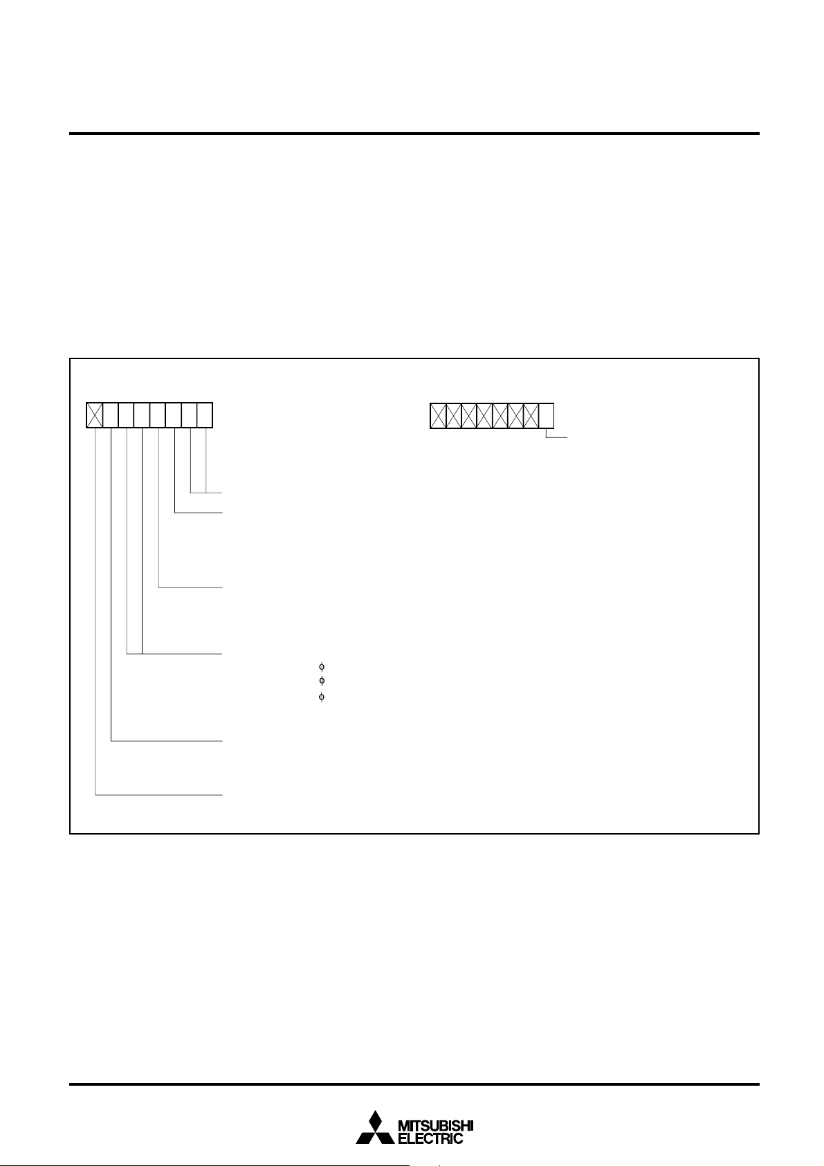
765432 01
0
10
Address
16
Processor mode register 0
Must be “10” (“10” after reset)
Wait bit
0 : Wait
1 : No wait
Software reset bit
Reset occurs when this bit is set to “1”
Interrupt priority detection time selection bit
0 0 : Internal clock ✕ 7 (cycle)
0 1 : Internal clock
1 0 : Internal clock ✕ 2 (cycle)
Must be “0”
Not used
5E
✕ 4 (cycle)
765432 01
Processor mode register 1
Wait selection bit
0 : Wait 0
1 : Wait 1
Address
5F16
Fig. 8 Processor mode register bit configuration
10
PRELIMINARY
Notice: This is not a final specification.
Some parametric limits are subject to change.
PM
1
PM
0
Mode
Pin
MITSUBISHI MICROCOMPUTERS
M37735S4BFP
16-BIT CMOS MICROCOMPUTER
1
0
Microprocessor mode
CS
RSMP
P10/A8/D
to
P17/A15/D
P20/A0/D
to
P27/A7/D
P3
P31/
P32/ALE,
P33/
0
to
8
15
0
7
0
/
RDE
CS
4
, A16, A
BYTE = “L”
BYTE = “H”
BYTE = “L”
BYTE = “H”
WEL,
WEH
,
HLDA
RDE
(Note)
RDE, WEL, WEH
P00/
CS
0
to
P04/
CS
17
RDE, WEL, WEH
RDE, WEL, WEH
RDE, WEL, WEH
RDE, WEL, WEH
P30/
P31/
P32/
P33/
P05/
P06/A
P07/A
P10/A8/D
7/A15 /D15
P1
P10/A8/D
7/A15/D15
P1
P20/A0/D
7/A7/D7
P2
P20/A0/D
7/A7/D7
P2
WEL
WEH
ALE
HLDA
RSMP
16
17
to
to
to
to
4
A8 to A
8
8
0
0
CS0 — CS
RSMP
Address A16, A
15
Address
Data(odd)
Address A8 – A
A0 to A
7
ALE
7
HLDA
Data(even)
Data
(odd,even)
WEL
WEH
Address
A0 to A
Address
4
17
15
(Note)
(Note)
RDE, WEL, WEH
HOLD
HOLD,
,
RDY
P42/1,
Ports P43 to P4
7
RDY
P42/
P4
1
3
to
P4
7
Fig. 9 Functions of pins P00/CS0 to P47 in microprocessor mode
Note. The signal output disable selection bit (bit 6 of the oscillation circuit control register 0) can stop the 1 output in the microprocessor
mode. In this mode, signals RDE, WEL, WEH can also be fixed to “H” when the internal memory area is accessed.
___
___ ___ ___
HOLD
RDY
(Note)
I/O Port
11
 Loading...