Mitsubishi M37733M4LXXXHP Datasheet
MITSUBISHI MICROCOMPUTERS
M37733M4LXXXHP
PRELIMINARY
Notice: This is not a final specification.
Some paramentic limits are suject to change.
SINGLE-CHIP 16-BIT CMOS MICROCOMPUTER
DESCRIPTION
The M37733M4LXXXHP is a single-chip microcomputer using the
7700 Family core. This single-chip microcomputer has a CPU and a
bus interface unit. The CPU is a 16-bit parallel processor that can be
an 8-bit parallel processor, and the bus interface unit enhances the
memory access efficiency to execute instructions fast. This
microcomputer also includes a 32 kHz oscillation circuit, in addition
to the ROM, RAM, multiple-function timers, serial I/O, A-D converter,
and so on.
Its strong points are the low power dissipation, the low supply voltage,
and the small package.
FEATURES
●Number of basic instructions .................................................. 103
●Memory size ROM ................................................. 32 Kbytes
RAM ................................................ 2048 bytes
●Instruction execution time
The fastest instruction at 12 MHz frequency ...................... 333 ns
●Single power supply ...................................................... 2.7–5.5 V
●Low power dissipation (At 3 V supply voltage, 12 MHz frequency)
............................................ 9 mW (Typ.)
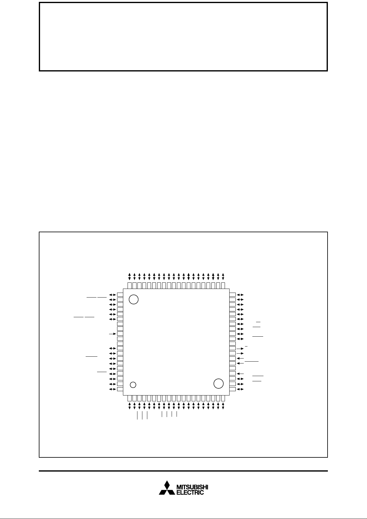
PIN CONFIGURATION (TOP VIEW)
1
1
D
D
x
0
1
2
3
4
5
/R
6
P8
x
/T
7
P8
/A
0
P0
/A
1
P0
/A
2
P0
/A
3
P0
/A
4
P0
/A
5
P0
6
/A
6
P0
●Interrupts ............................................................ 19 types, 7 levels
●Multiple-function 16-bit timer ................................................. 5 + 3
●Serial I/O (UART or clock synchronous) ..................................... 3
●10-bit A-D converter .............................................. 8-channel inputs
●12-bit watchdog timer
●Programmable input/output
(ports P0, P1, P2, P3, P4, P5, P6, P7, P8) ............................... 68
●Clock generating circuit ........................................ 2 circuits built-in
●Small package ..................... 80-pin plastic molded fine-pitch QFP
(80P6D-A;0.5 mm lead pitch)
APPLICATION
Control devices for general commercial equipment such as office
automation, office equipment, personal information equipment, and
so on.
Control devices for general industrial equipment such as
communication equipment, and so on.
10
11
12
13
14
15
0
7
/A
7
P0
8
/D
8
/A
0
P1
9
/D
9
/A
1
P1
/D
10
/A
2
P1
/D
11
/A
3
P1
/D
12
/A
4
P1
/D
13
/A
5
P1
/D
14
/A
6
P1
/D
15
/A
7
P1
/D
16
/A
0
P2
1
/D
17
/A
1
P2
P85/CLK
P84/CTS1/RTS
P83/TXD
P82/RXD0/CLKS
P81/CLK
P80/CTS0/RTS0/CLKS
AV
V
AV
P77/AN7/X
P76/AN6/X
P75/AN5/AD
COUT
TRG/TXD2
P74/AN4/RXD
P73/AN3/CLK
P72/AN2/CTS
P71/AN
P70/AN
P67/TB2IN/φ
V
V
REF
CIN
SUB
49
12
IN
/TA1
3
P5
48
13
OUT
/TA1
2
P5
47
14
IN
/TA0
1
P5
46
15
OUT
/TA0
0
P5
45
16
7
P4
58
57
59
60
61
1
62
1
63
0
64
0
65
0
66
1
67
CC
68
CC
69
70
SS
71
SS
72
73
74
75
2
76
2
77
2
78
1
79
0
80
1
IN
/TB1
6
P6
56
55
M37733M4LXXXHP
4
6
3
5
2
2
1
0
IN
/TB0
5
P6
/INT
4
P6
/INT
3
P6
/INT
2
P6
IN
/TA4
1
P6
54
7
OUT
/TA4
0
P6
53
8
3
/KI
IN
/TA3
7
P5
52
9
2
/KI
OUT
/TA3
6
P5
51
10
1
/KI
IN
/TA2
5
P5
50
11
0
/KI
OUT
/TA2
4
P5
41
42
44
43
40
P22/A18/D
P23/A19/D
P24/A20/D
P25/A21/D
P26/A22/D
P27/A23/D
P30/R/W
1
/BHE
P3
P32/ALE
P3
3
/HLDA
V
SS
E
OUT
X
IN
X
RESET
CNV
SS
BYTE
P4
0
/HOLD
P41/RDY
P42/φ
1
2
3
4
5
6
7
39
38
37
36
35
34
33
32
31
30
29
28
27
26
25
24
23
22
21
20
17
19
18
5
6
3
4
P4
P4
P4
P4
Outline 80P6D-A
MITSUBISHI MICROCOMPUTERS
M37733M4LXXXHP
PRELIMINARY
Notice: This is not a final specification.
Some paramentic limits are suject to change.
SINGLE-CHIP 16-BIT CMOS MICROCOMPUTER
Data Bus(Even)
Data Bus(Odd)
BYTE
selection input
External data bus width
VREF
Reference
voltage input
AVCC
(0V)
AVSS
CNVss
SS
V
(0V)
VCC
Instruction Register(8)
Data Buffer DB
H
(8)
Data Buffer DBL(8)
Instruction Queue Buffer Q
Instruction Queue Buffer Q
Instruction Queue Buffer Q2(8)
0(8)
1(8)
Incrementer(24)
Program Address Register PA(24)
Data Address Register DA(24)
Incrementer/Decrementer(24)
Program Counter PC(16)
Program Bank Register PG(8)
Data Bank Register DT(8)
Input Butter Register IB(16)
Address Bus
UART2(9)
UART1(9)
A-D Converter(10)
UART0(9)
P0(8)
P1(8)
P2(8)
P4(8) P3(4)
Input/Output
port P0
Input/Output
port P1
Input/Output
port P2
Input/Output
port P3
Input/Output
port P4
Processor Status Register PS(11)
Direct Page Register DPR(16)
RESET
Reset input
Stack Pointer S(16)
Index Register Y(16)
XCOUT
XCIN
Index Register X(16)
Accumulator B(16)
E
output
Enable
XOUT
Clock output
XIN
Clock input
Clock Generating Circuit
Accumulator A(16)
Arithmetic Logic
Unit(16)
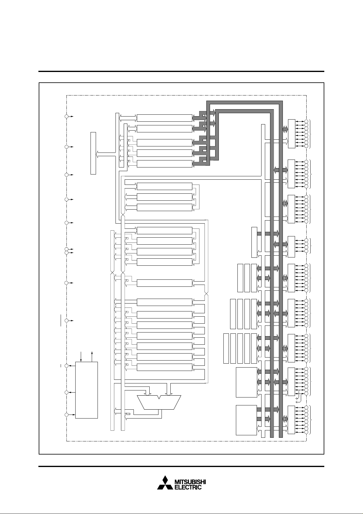
M37733M4LXXXHP BLOCK DIAGRAM
Timer TB2(16)
Watchdog Timer
Timer TA3(16)
Timer TA4(16)
Timer TA2(16)
RAM
ROM
Timer TB0(16)
Timer TB1(16)
Timer TA1(16)
Timer TA0(16)
2048 bytes
32 Kbytes
XCOUT
XCIN
P5(8)P6(8)
P7(8)
P8(8)
Input/Output
port P5
Input/Output
port P6
Input/Output
port P7
Input/Output
port P8
2

MITSUBISHI MICROCOMPUTERS
M37733M4LXXXHP
PRELIMINARY
Notice: This is not a final specification.
Some paramentic limits are suject to change.
FUNCTIONS OF M37733M4LXXXHP
Number of basic instructions 103
Instruction execution time 333 ns (the fastest instruction at external clock 12 MHz frequency)
Memory size
Input/Output ports
Multi-function timers
Serial I/O (UART or clock synchronous serial I/O) ✕ 3
A-D converter 10-bit ✕ 1 (8 channels)
Watchdog timer 12-bit ✕ 1
Interrupts
Clock generating circuit
Supply voltage 2.7 – 5.5 V
Power dissipation
Input/Output characteristic
Memory expansion Maximum 16 Mbytes
Operating temperature range –40 to 85 °C
Device structure CMOS high-performance silicon gate process
Package 80-pin plastic molded fine-pitch QFP (80P6D-A;0.5 mm lead pitch)
Parameter Functions
ROM 32 Kbytes
RAM 2048 bytes
P0 – P2, P4 – P8 8-bit ✕ 8
P3 4-bit ✕ 1
TA0, TA1, TA2, TA3, TA4 16-bit ✕ 5
TB0, TB1, TB2 16-bit ✕ 3
3 external types, 16 internal types
Each interrupt can be set to the priority level (0 – 7.)
2 circuits built-in (externally connected to a ceramic resonator or a
quartz-crystal oscillator)
9 mW (at 3 V supply voltage, external clock 12 MHz frequency)
22.5 mW (at 5 V supply voltage, external clock 12 MHz frequency)
Input/Output voltage 5 V
Output current 5 mA
SINGLE-CHIP 16-BIT CMOS MICROCOMPUTER
3

MITSUBISHI MICROCOMPUTERS
M37733M4LXXXHP
PRELIMINARY
Notice: This is not a final specification.
Some paramentic limits are suject to change.
PIN DESCRIPTION
Pin Name Input/Output Functions
Vcc, Power source Apply 2.7 – 5.5 V to Vcc and 0 V to Vss.
Vss
CNVss CNVss input Input This pin controls the processor mode. Connit to Vss for the single-chip mode and the memory
_________________
RESET Reset input Input When “L” level is applied to this pin, the microcomputer enters the reset state.
XIN Clock input Input
X
OUT Clock output Output
______
E Enable output Output This pin functions as the enable signal output pin which indicates the access status in the internal
BYTE
External data
Input In the memory expansion mode or the microprocessor mode, this pin determinis whether the
bus width
selection input
AVcc, Analog power Power source input pin for the A-D converter. Externally connict AVcc to Vcc and AVss to Vss.
AVss source input
REF Reference Input This is reference voltage input pin for the A-D converter.
V
voltage input
0 – P07 I/O port P0 I/O In the single-chip mode, port P0 becomes an 8-bit I/O port. An I/O direction register is available so
P0
0 – P17 I/O port P1 I/O In the single-chip mode, these pins have the same functions as port P0. When the BYTE pin is set
P1
0 – P27 I/O port P2 I/O In the single-chip mode, these pins have the same functions as port P0. In the memory expansion
P2
0 – P33 I/O port P3 I/O In the single-chip mode, these pins have the same function as port P0. In the memory expansion
P3
0 – P47 I/O port P4 I/O In the single-chip mode, these pins have the same functions as port P0. In the memory expansion
P4
0 – P57 I/O port P5 I/O In addition to having the same functions as port P0 in the single-chip mode, these pins also
P5
0 – P67 I/O port P6 I/O In addition to having the same functions as port P0 in the single-chip mode, these pins also
P6
0 – P77 I/O port P7 I/O In addition to having the same functions as port P0 in the single-chip mode, these pins function
P7
0 – P87 I/O port P8 I/O In addition to having the same functions as port P0 in the single-chip mode, these pins also
P8
expansion mode, and to Vcc for the microprocessor mode.
These are pins of main-clock genirating circuit. Connict a ceramic resonator or a quartzcrystal oscillator between X
IN and XOUT. When an external clock is used, the clock source should
be connected to the XIN pin, and the XOUT pin should be left open.
bus. When output level of E signal is “L”, data/instruction read or data write is performed.
___
external data bus has an 8-bit width or a 16-bit width. The data bus has a 16-bit width when “L”
signal is input and an 8-bit width when “H” signal is input.
that each pin can be programmed for input or output. These ports are in the input mode when
reset.
In the memory expansion mode or the microprocessor mode, these pins output address (A0 – A7).
to “L” in the memory expansion mode or the microprocessor mode and external data bus has a
16-bit width, high-order data (D8 – D15) is input/output or an address (A8 – A15) is output. When
the BYTE pin is “H” and an external data bus has an 8-bit width, only address (A8 – A15) is output.
mode or the microprocessor mode, low-order data (D
(A16 – A23) is output.
mode or the microprocessor mode, R/W, BHE, ALE, and HLDA signals are output.
mode or the microprocessor mode, P40, P41, and P42 become HOLD and RDY input pins, and
clock
φ1 output pin, respectively.
Functions of the other pins are the same as in the single-chip mode. However, in the memory
expansion mode, P42 also functions as an I/O port.
function as I/O pins for timers A0 to A3 and input pins for key input interrupt input (KI0 – KI3).
function as I/O pins for timer A4, input pins for external interrupt input (INT0 – INT2) and input pins
for timers B0 to B2. P67 also functions as sub-clock φSUB output pin.
as input pins for A-D converter. P7
and P77 have the function as the output pin (XCOUT) and the input pin (XCIN) of the sub-clock
(32 kHz) oscillation circuit, respectively. When P7
connect a resonator or an oscillator between the both.
function as I/O pins for UART 0 and UART 1.
SINGLE-CHIP 16-BIT CMOS MICROCOMPUTER
0 – D7) is input/output or an address
____________ ______
_______________
_________________
________________
2 to P75 also function as I/O pins for UART2. Additionally, P76
6 and P77 are used as the XCOUT and XCIN pins,
4
MITSUBISHI MICROCOMPUTERS
M37733M4LXXXHP
PRELIMINARY
Notice: This is not a final specification.
Some paramentic limits are suject to change.
SINGLE-CHIP 16-BIT CMOS MICROCOMPUTER
BASIC FUNCTION BLOCKS
The M37733M4LXXXHP has the same functions as the
M37733MHBXXXFP except for the memory allocation, the reset
circuit, the ROM area modification function, and the package.
Refer to the section on the M37733MHBXXXFP.
MEMORY
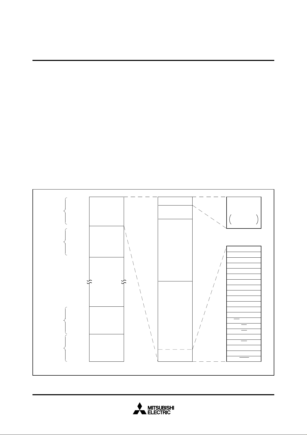
The memory map is shown in Figure 1. The address space has a
capacity of 16 Mbytes and is allocated to addresses from 0
FFFFFF
16. The address space is divided by 64-Kbyte unit called bank.
The banks are numbered from 0
16 to FF16.
Built-in ROM, RAM and control registers for internal peripheral devices
are assigned to bank 0
The 32-Kbyte area from addresses 8000
ROM. Addresses FFD6
16.
16 to FFFF16 is the built-in
16 to FFFF16 are the RESET and interrupt
vector addresses and contain the interrupt vectors. Refer to the section
on interrupts for details.
The 2048-byte area allocated to addresses from 80
16 to 87F16 is the
built-in RAM. In addition to storing data, the RAM is used as stack
during a subroutine call or interrupts.
000000
16
Bank 0
16
00FFFF
16
010000
16
16 to
000000
00007F
000080
00087F
Peripheral devices such as I/O ports, A-D converter, serial I/O, timer,
and interrupt control registers are allocated to addresses from 0
7F
16.
Additionally, the internal ROM area can be modified by software. Refer
to the section on ROM area modification function for details.
A 256-byte direct page area can be allocated anywhere in bank 0
by using the direct page register (DPR). In the direct page addressing
mode, the memory in the direct page area can be accessed with two
words. Hence program steps can be reduced.
16
16
16
16
Internal RAM
2048 bytes
000000
00007F
16
Internal peripheral
devices
control registers
refer to Fig. 2 for
detail information
16
16 to
16
Bank 1
16
01FFFF
16
• • • • • • • • • • • • • • • • • • •
008000
16
FE0000
Bank FE
Bank FF
16
16
FEFFFF
16
FF0000
16
16
FFFFFF
16
00FFD6
00FFFF
Internal ROM
32 Kbytes
16
16
Note. Internal ROM area can be modified. (Refer to the section on ROM area modification function.)
Fig. 1 Memory map
00FFD6
00FFFE
Interrupt vector table
16
A-D/UART2 trans./rece.
UART1 transmission
UART1 receive
UART0 transmission
UART0 receive
Timer B2
Timer B1
Timer B0
Timer A4
Timer A3
Timer A2
Timer A1
Timer A0
INT
2
/Key input
INT
1
INT
0
Watchdog timer
DBC
BRK instruction
Zero divide
16
RESET
5

MITSUBISHI MICROCOMPUTERS
M37733M4LXXXHP
PRELIMINARY
Notice: This is not a final specification.
Some paramentic limits are suject to change.
SINGLE-CHIP 16-BIT CMOS MICROCOMPUTER
Address (Hexadecimal notation)
000000
000001
000002
000003
000004
000005
000006
000007
000008
000009
00000A
00000B
00000C
00000D
00000E
00000F
000010
000011
000012
000013
000014
Port P0 register
Port P1 register
Port P0 direction register
Port P1 direction register
Port P2 register
Port P3 register
Port P2 direction register
Port P3 direction register
Port P4 register
Port P5 register
Port P4 direction register
Port P5 direction register
Port P6 register
Port P7 register
Port P6 direction register
Port P7 direction register
Port P8 register
Port P8 direction register
000015
000016
000017
000018
000019
00001A
00001B
00001C
00001D
00001E
00001F
000020
000021
000022
000023
000024
000025
000026
000027
000028
000029
00002A
00002B
00002C
00002D
00002E
00002F
000030
000031
000032
000033
000034
000035
000036
000037
000038
000039
00003A
00003B
00003C
00003D
00003E
00003F
Reserved area (Note)
Reserved area (Note)
A-D control register 0
A-D control register 1
A-D register 0
A-D register 1
A-D register 2
A-D register 3
A-D register 4
A-D register 5
A-D register 6
A-D register 7
UART 0 transmit/receive mode register
UART 0 baud rate register
UART 0 transmission buffer register
UART 0 transmit/receive control register 0
UART 0 transmit/receive control register 1
UART 0 receive buffer register
UART 1 transmit/receive mode register
UART 1 baud rate register
UART 1 transmission buffer register
UART 1 transmit/receive control register 0
UART 1 transmit/receive control register 1
UART 1 receive buffer register
Fig. 2 Location of internal peripheral devices and interrupt control registers
Address (Hexadecimal notation)
000040
000041
000042
000043
000044
Count start flag
One-shot start flag
Up-down flag
000045
000046
000047
000048
000049
00004A
00004B
00004C
00004D
00004E
00004F
000050
000051
000052
000053
000054
000055
000056
000057
000058
000059
00005A
00005B
00005C
00005D
00005E
00005F
000060
000061
000062
000063
000064
000065
000066
000067
000068
000069
00006A
00006B
00006C
00006D
00006E
00006F
000070
000071
000072
000073
000074
000075
000076
000077
000078
000079
00007A
00007B
00007C
00007D
00007E
00007F
Timer A0 register
Timer A1 register
Timer A2 register
Timer A3 register
Timer A4 register
Timer B0 register
Timer B1 register
Timer B2 register
Timer A0 mode register
Timer A1 mode register
Timer A2 mode register
Timer A3 mode register
Timer A4 mode register
Timer B0 mode register
Timer B1 mode register
Timer B2 mode register
Processor mode register 0
Processor mode register 1
Watchdog timer register
Watchdog timer frequency selection flag
Reserved area (Note)
Memory allocation control register
UART 2 transmit/receive mode register
UART 2 baud rate register
UART 2 transmission buffer register
UART 2 transmit/receive control register 0
UART 2 transmit/receive control register 1
UART 2 receive buffer register
Oscillation circuit control register 0
Port function control register
Serial transmit control register
Oscillation circuit control register 1
A-D/UART 2 trans./rece. interrupt control register
UART 0 transmission interrupt control register
UART 0 receive interrupt control register
UART 1 transmission interrupt control register
UART 1 receive interrupt control register
Timer A0 interrupt control register
Timer A1 interrupt control register
Timer A2 interrupt control register
Timer A3 interrupt control register
Timer A4 interrupt control register
Timer B0 interrupt control register
Timer B1 interrupt control register
Timer B2 interrupt control register
INT
0
interrupt control register
INT
1
interrupt control register
INT
2
/Key input interrupt control register
Note. Do not write to this address.
6

MITSUBISHI MICROCOMPUTERS
M37733M4LXXXHP
PRELIMINARY
Notice: This is not a final specification.
Some paramentic limits are suject to change.
SINGLE-CHIP 16-BIT CMOS MICROCOMPUTER
RESET CIRCUIT
The microcomputer is released from the reset state when the RESET
_____________
pin is returned to “H” level after holding it at “L” level with the power
source voltage at 2.7 – 5.5 V. Program execution starts at the address
formed by setting address A
of address FFFF
16, and A7 – A0 to the contents of address FFFE16.
23 – A16 to 0016, A15 – A8 to the contents
Figure 3 shows an example of a reset circuit. When the stabilized
clock is input from the external to the main-clock oscillation circuit,
the reset input voltage must be 0.55 V or less when the power source
voltage reaches 2.7 V. When a resonator/oscillator is connected to
the main-clock oscillation circuit, change the reset input voltage from
“L” to “H” after the main-clock oscillation is fully stabilized.
The status of the internal registers during reset is the same as the
M37733MHBXXXFP’s.
Power on
RESET
V
CC
V
CC
0V
RESET
0V
2.7V
0.55V
Note. In this case, stabilized clock is input from the
external to the main-clock oscillation circuit.
Perform careful evalvation at the system design
level before using.
Fig. 3 Example of a reset circuit
7
MITSUBISHI MICROCOMPUTERS
M37733M4LXXXHP
PRELIMINARY
Notice: This is not a final specification.
Some paramentic limits are suject to change.
SINGLE-CHIP 16-BIT CMOS MICROCOMPUTER
ROM AREA MODIFICATION FUNCTION
The internal ROM size and its address area of the M37733M4LXXXHP
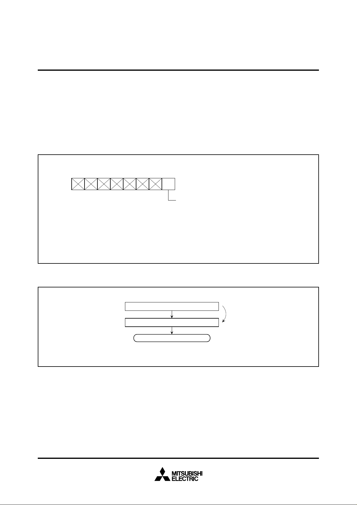
can be modified by the memory allocation control register’s bit 0 shown
in Figure 4.
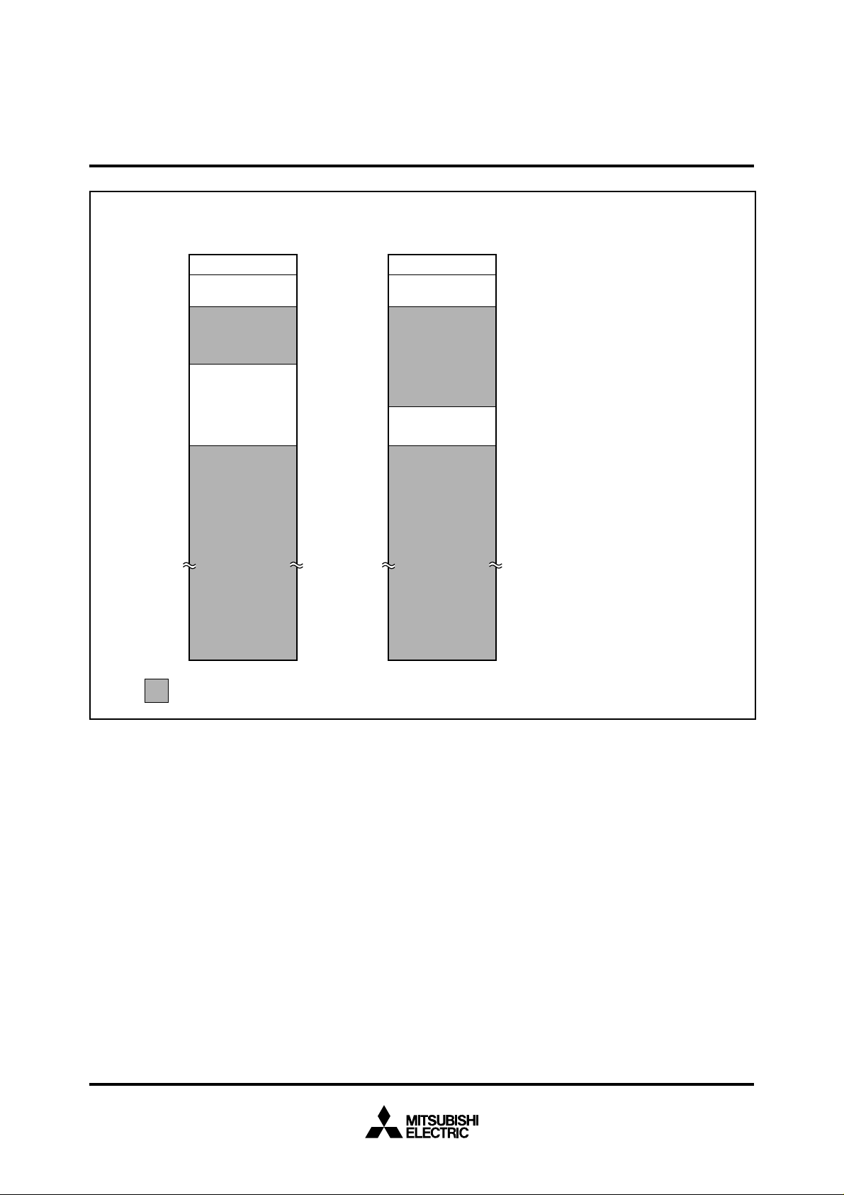
Figure 6 shows the memory allocation in which the internal ROM
size and its address area are modified.
Make sure to write data in the memory allocation control register as
the flow shown in Figure 5.
This ROM area modification function is valid in memory expansion
mode and single-chip mode.
76543210
ML
Note. Write to the memory allocation control register as the flow shown in Figure 5.
When ordering a mask ROM, Mitsubishi Electric corp. produces the
mask ROM using the data within 32 Kbytes (addresses 008000
00FFFF
16). It is regardless of the selected ROM size (refer to MASK
ROM ORDER CONFIRMATION FORM.) Therefore, program “FF
to the addresses out of the selected ROM area in the EPROM which
you tender when ordering a mask ROM.
Address 00FFFF
16 of this microcomputer corresponds to the lowest
address of the EPROM which you tender.
0
Memory allocation control register
Address
63
16
Memory allocation selection bit
ROM size (ROM area)
16
0 : 32 Kbytes (addresses 008000
1 : 16 Kbytes (addresses 00C000
– 00FFFF16)
16
– 00FFFF16)
16 –
16”
Fig. 4 Bit configuration of memory allocation control register
Writing data “5516” (LDM instruction)
Writing data “0016” or “0116” (LDM instruction)
• How to write in memory allocation control register
Fig. 5 How to write data in memory allocation control register
0
selection bit
ML
Next instruction
8
MITSUBISHI MICROCOMPUTERS
M37733M4LXXXHP
PRELIMINARY
Notice: This is not a final specification.
Some paramentic limits are suject to change.
0
) = (0) (ML0) = (1)
(ML
ROM size : 32 Kbytes ROM size : 16 Kbytes
000000
00007F
000080
00087F
008000
16
16
16
16
16
SFR
Internal RAM
2048 bytes
000000
00007F
000080
00087F
16
16
16
16
SFR
Internal RAM
2048 bytes
SINGLE-CHIP 16-BIT CMOS MICROCOMPUTER
Internal ROM
00C000
00FFFF
010000
FFFFFF
32 Kbytes
16
16
16
00FFFF
010000
FFFFFF
16
16
16
16
Internal ROM
16 Kbytes
: External memory area
Fig. 6 Memory allocation (modification of internal ROM area by memory allocation selection bit)
ADDRESSING MODES
The M37733M4LXXXHP has 28 powerful addressing modes. Refer
to the SINGLE-CHIP 16-BIT MICROCOMPUTERS DATA BOOK for
the details of each addressing mode.
MACHINE INSTRUCTION LIST
The M37733M4LXXXHP has 103 machine instructions. Refer to the
SINGLE-CHIP 16-BIT MICROCOMPUTERS DATA BOOK for details.
DATA REQUIRED FOR MASK ROM ORDERING
Please send the following data for mask orders.
(1) M37733M4LXXXHP mask ROM order confirmation form
(2) 80P6D mark specification form
(3) ROM data (EPROM 3 sets)
9

MITSUBISHI MICROCOMPUTERS
M37733M4LXXXHP
PRELIMINARY
Notice: This is not a final specification.
Some paramentic limits are suject to change.
ABSOLUTE MAXIMUM RATINGS
Symbol Parameter Conditions Ratings Unit
Vcc Power source voltage –0.3 to +7 V
AVcc Analog power source voltage –0.3 to +7 V
VI
Input voltage RESET, CNVss, BYTE –0.3 to +12 V
Input voltage P0
V
I
Output voltage
VO
Pd Power dissipation Ta = 25 °C 200 mW
Topr Operating temperature –40 to +85 °C
stg Storage temperature –65 to +150 °C
T
_____________
0 – P07, P10 – P17, P20 – P27,
0 – P33, P40 – P47, P50 – P57,
P3
0 – P67, P70 – P77, P80 – P87,
P6
VREF, XIN
P00 – P07, P10 – P17, P20 – P27,
0 – P33, P40 – P47, P50 – P57,
P3
0 – P67, P70 – P77, P80 – P87,
P6
___
XOUT, E
SINGLE-CHIP 16-BIT CMOS MICROCOMPUTER
–0.3 to Vcc + 0.3 V
–0.3 to Vcc + 0.3 V
RECOMMENDED OPERATING CONDITIONS (Vcc = 2.7 – 5.5 V, Ta = –40 to +85 °C, unless otherwise noted)
Symbol Parameter
IN) : Operating 2.7 5.5
Vcc Power source voltage
f(X
f(XIN) : Stopped, f(XCIN) = 32.768 kHz 2.7 5.5
Min. Typ. Max.
AVcc Analog power source voltage Vcc V
Vss Power source voltage 0V
AVss Analog power source voltage 0 V
IH
V
VIH
VIH
VIL
VIL
VIL
IOH(peak)
High-level input voltage P0
P70 – P77, P80 – P87, XIN, RESET, CNVss, BYTE, XCIN (Note 3)
High-level input voltage P10 – P17, P20 – P27 (in single-chip mode)
High-level input voltage P1
(in memory expansion mode and microprocessor mode)
Low-level input voltage P0
P70 – P77, P80 – P87, XIN, RESET, CNVss, BYTE, XCIN (Note 3)
Low-level input voltage P10 – P17, P20 – P27 (in single-chip mode)
Low-level input voltage P1
(in memory expansion mode and microprocessor mode)
High-level peak output current P0
0 – P07, P30 – P33, P40 – P47, P50 – P57, P60 – P67,
0 – P17, P20 – P27
0 – P07, P30 – P33, P40 – P47, P50 – P57, P60 – P67,
0 – P17, P20 – P27
0 – P07, P10 – P17, P20 – P27, P30 – P33,
0 – P47, P50 – P57, P60 – P67, P70 – P77,
P4
____________
_____________
0.8 Vcc
0.8 Vcc
0.5 Vcc
0
0
0
P80 – P87
High-level average output current P00 – P07, P10 – P17, P20 – P27, P30 – P33,
IOH(avg)
P4
0 – P47, P50 – P57, P60 – P67, P70 – P77,
P80 – P87
Low-level peak output current P00 – P07, P10 – P17, P20 – P27, P30 – P33,
IOL(peak)
0 – P43, P54 – P57, P60 – P67, P70 – P77,
P4
P80 – P87
IOL(peak)
Low-level peak output current P44 – P47, P50 – P53
Low-level average output current P00 – P07, P10 – P17, P20 – P27, P30 – P33,
0 – P43, P54 – P57, P60 – P67, P70 – P77,
IOL(avg)
P4
P80 – P87
IOL(avg) Low-level average output current P44 – P47, P50 – P53 12 mA
f(XIN) Main-clock oscillation frequency (Note 4) 12 MHz
CIN) Sub-clock oscillation frequency 32.768 50 kHz
f(X
Notes 1. Average output current is the average value of a 100 ms interval.
2. The sum of I
the sum of I
the sum of I
the sum of I
3. Limits V
4. The maximum value of f(X
OL(peak) for ports P0, P1, P2, P3, and P8 must be 80 mA or less,
OH(peak) for ports P0, P1, P2, P3, and P8 must be 80 mA or less,
OL(peak) for ports P4, P5, P6, and P7 must be 100 mA or less, and
OH(peak) for ports P4, P5, P6, and P7 must be 80 mA or less.
IH and VIL for XCIN are applied when the sub clock external input selection bit = “1”.
IN) = 6 MHz when the main clock division selection bit = “1”.
Limits
Vcc
Vcc
Vcc
0.2Vcc
0.2Vcc
0.16Vcc
–10
–5
10
16
5
Unit
V
V
V
V
V
V
V
mA
mA
mA
mA
mA
10
 Loading...