

MITSUBISHI MICROCOMPUTERS
M37702M2AXXXFP, M37702M2BXXXFP
M37702M2-XXXFP and
M37702S1FP are respectively
unified into M37702M2AXXXFP
and M37702S1AFP.
M37702S1AFP, M37702S1BFP
SINGLE-CHIP 16-BIT CMOS MICROCOMPUTER
DESCRIPTION
The M37702M2AXXXFP is a single-chip microcomputers
designed with high-performance CMOS silicon gate technology.
This is housed in a 80-pin plastic molded QFP. This single-chip
microcomputer has a large 16 M bytes address space, three instruction queue buffers, and two data buffers for high-speed
instruction execution. The CPU is a 16-bit parallel processor that
can also be switched to perform 8-bit parallel processing. This
microcomputer is suitable for office, business, and industrial
equipment controller that require high-speed processing of large
data.
The differences between M37702M2AXXXFP, M37702M2BXXXFP,
M37702S1AFP and M37702S1BFP are the ROM size and the external clock input frequency as shown below. Therefore, the
following descriptions will be for the M37702M2AXXXFP unless
otherwise noted.
Type name
M37702M2AXXXFP
M37702M2BXXXFP
M37702S1AFP
M37702S1BFP
ROM size
16 K bytes
16 K bytes
External
External
External clock input frequency
16 MHz
25 MHz
16 MHz
25 MHz
FEATURES
• Number of basic instructions ..................................................103
• Memory size ROM ................................................ 16 K bytes
RAM ................................................. 512 bytes
• Instruction execution time
M37702M2AXXXFP, M37702S1AFP
(The fastest instruction at 16 MHz frequency) .................. 250 ns
M37702M2BXXXFP, M37702S1BFP
(The fastest instruction at 25 MHz frequency) .................. 160 ns
• Single power supply..................................................... 5 V ± 10%
• Low power dissipation (at 16 MHz frequency)
......................................... 60 mW ( Typ.)
• Interrupts............................................................19 types 7 levels
• Multiple function 16-bit timer ................................................ 5 + 3
• UART (may also be synchronous).............................................. 2
• 8-bit A-D converter ............................................. 8-channel inputs
• 12-bit watchdog timer.
• Programmable input/output
(ports P0, P1, P2, P3, P4, P5, P6, P7, P8) .............................. 68
APPLICATION
Control devices for office equipment such as copiers, printers,
typewriters, facsimiles, word processors, and personal computers
Control devices for industrial equipment such as ME, NC, communication and measuring instruments.
NOTE
Refer to “Chapter 5 PRECAUTIONS” when using this microcomputer.
The M37702M2AXXXFP and M37702S1AFP satisfy the timing
requirements and the switching characteristics of the former
M37702M2-XXXFP and M37702S1FP.
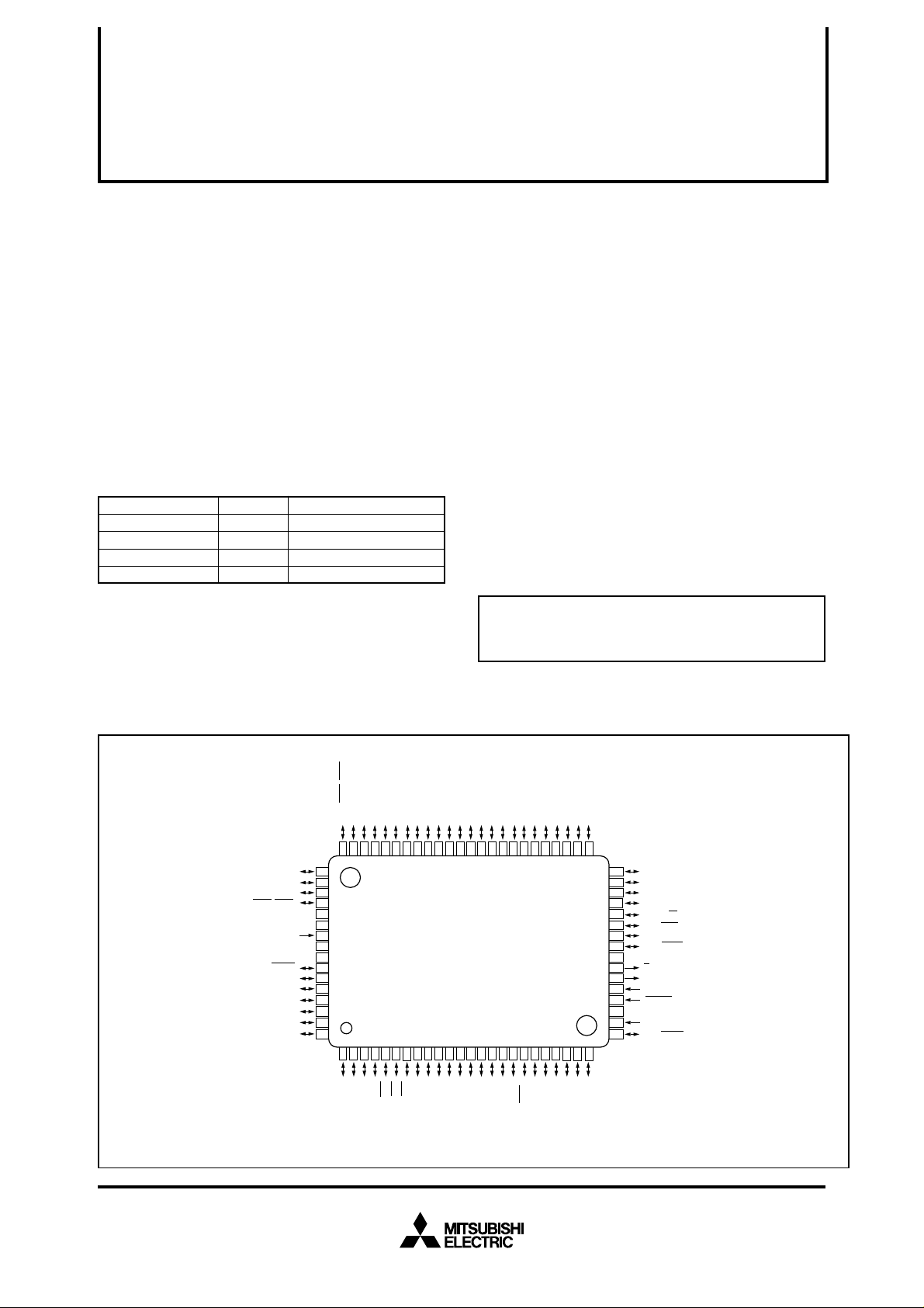
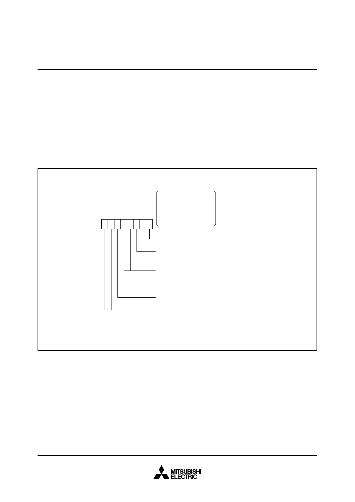
PIN CONFIGURATION (TOP VIEW)
P83/TXD
0
P82/RXD
0
P81/CLK
0
/CTS0/RTS
P76/AN
P75/AN
P74/AN
P73/AN
P72/AN
P71/AN
0
0
V
CC
AV
CC
V
REF
AV
SS
V
SS
TRG
6
5
4
3
2
1
P8
P77/AN7/AD
1
RTS
/
1
CTS
/
4
P8
64
65
66
67
6
8
69
70
71
72
73
74
75
76
77
78
79
80
1
0
/AN
0
P7
1
1
1
D
D
/CLK
5
P8
63
2
IN
/TB2
7
P6
X
/R
6
P8
62
3
IN
/TB1
6
P6
X
/T
7
P8
61
4
IN
/TB0
5
P6
0
1
A
A
/
/
0
1
P0
P0
59
60
6
5
2
1
NT
NT
/I
/I
4
3
P6
P6
6
2
A
/
2
P0
58
M37702M2AXXXFP
M37702M2BXXXFP
7
0
NT
/I
2
P6
7
3
4
5
A
A
A
/
/
/
/A
/A
3
4
5
6
7
P0
P0
P0
P0
P0
56
54
55
53
57
or
or
M37702S1AFP
or
M37702S1BFP
8
10
12
9
11
IN
IN
IN
OUT
OUT
/TA4
/TA3
/TA2
1
7
5
/TA4
/TA3
0
6
P6
P5
P5
P6
P5
Outline 80P6N-A
✽ : Used in the evaluation chip mode only
8
/D
8
/A
0
P1
52
13
OUT
/TA2
4
P5
9
/D
9
/A
1
P1
51
14
IN
/TA1
3
P5
10
/D
10
/A
2
P1
50
15
OUT
/TA1
2
P5
11
/D
11
/A
3
P1
49
16
IN
/TA0
1
P5
12
/D
12
/A
4
P1
48
17
OUT
/TA0
0
P5
13
/D
13
/A
5
P1
47
18
✽
/DBC
7
P4
14
/D
14
/A
6
P1
46
19
✽
/VPA
6
P4
15
/D
15
/A
7
P1
45
20
✽
/VDA
5
P4
0
/D
16
/A
0
P2
44
21
✽
/QCL
4
P4
43
22
✽
1
/D
17
/A
1
P2
/MX
3
P4
2
3
/D
/D
18
19
/A
/A
2
3
P2
P2
41
42
40
P24/A20/D
P25/A21/D
P26/A22/D
P27/A23/D
P30/
R/W
P31/
BHE
P32/
ALE
P33/
HLDA
V
ss
E
X
OUT
IN
X
RESET
CNV
SS
BYTE
P40/
HOLD
4
5
6
7
39
38
37
36
35
34
33
32
31
30
29
28
27
26
25
24
23
1
/ φ
RDY
2
/
1
P4
P4
X
IN
X
OUT
E
RESET
Reset input
V
REF
P8(8) P7(8) P5(8)P6(8) P4(8) P3(4)
P2(8)
P1(8)
CNVss
BYTE
P0(8)
UART1(9)
UART0(9)
AV
SS
(0V)
AV
CC
(0V)
V
SS
V
CC
A-D Converter(8)
Clock input Clock output
Enable output
Reference
voltage input
Bus width
selection input
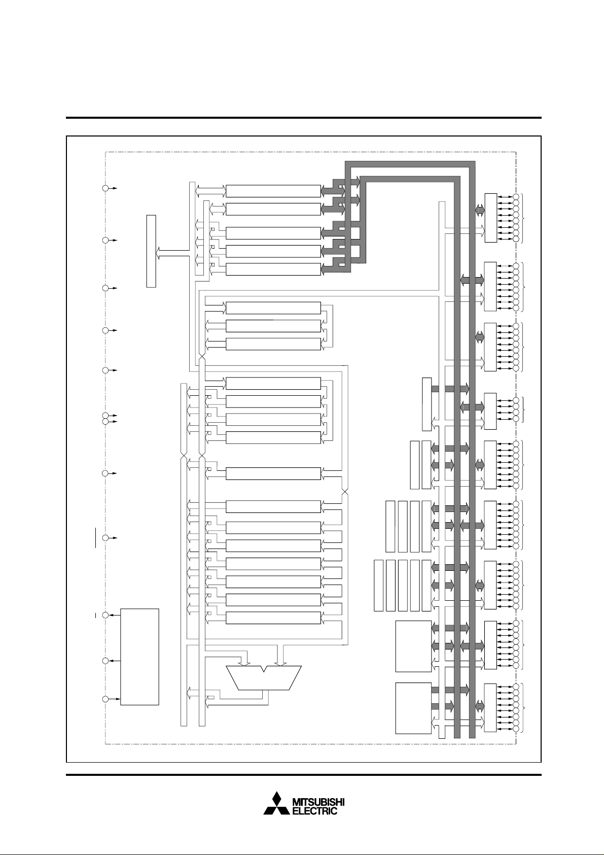
Clock Generating Circuit
Instruction Register(8)
Arithmetic Logic
Unit(16)
Accumulator A(16)
Accumulator B(16)
Index Register X(16)
Index Register Y(16)
Stack Pointer S(16)
Direct Page Register DPR(16)
Processor Status Register PS(11)
Input Buffer Register IB(16)
Data Bank Register DT(8)
Program Bank Register PG(8)
Program Counter PC(16)
Incrementer/Decrementer(24)
Data Address Register DA(24)
Program Address Register PA(24)
Incrementer(24)
Instruction Queue Buffer Q
2
(8)
Instruction Queue Buffer Q
1
(8)
Instruction Queue Buffer Q
0
(8)
Data Buffer DB
L
(8)
Data Buffer DB
H
(8)
ROM
16K Bytes
RAM
512 Bytes
Timer TA3(16)
Timer TA4(16)
Timer TA2(16)
Timer TA1(16)
Timer TA0(16)
Watchdog Timer
Timer TB2(16)
Timer TB1(16)
Timer TB0(16)
Address Bus
Data Bus(Odd)
Data Bus(Even)
Input/Output
port P8
Input/Output
port P7
Input/Output
port P6
Input/Output
port P5
Input/Output
port P4
Input/Output
port P3
Input/Output
port P2
Input/Output
port P1
Input/Output
port P0
29 30 31 28
69
32 73 27
(5V) (0V)
72 70
(5V)
71 26
60595857565554535251504948474645444342414039383725242322212019181716151413121110987654321807978777675746867666564636261 36353433
MITSUBISHI MICROCOMPUTERS
M37702M2AXXXFP, M37702M2BXXXFP
M37702S1AFP, M37702S1BFP
SINGLE-CHIP 16-BIT CMOS MICROCOMPUTER
M37702M2AXXXFP BLOCK DIAGRAM
2
MITSUBISHI MICROCOMPUTERS
M37702M2AXXXFP, M37702M2BXXXFP
M37702S1AFP, M37702S1BFP
SINGLE-CHIP 16-BIT CMOS MICROCOMPUTER
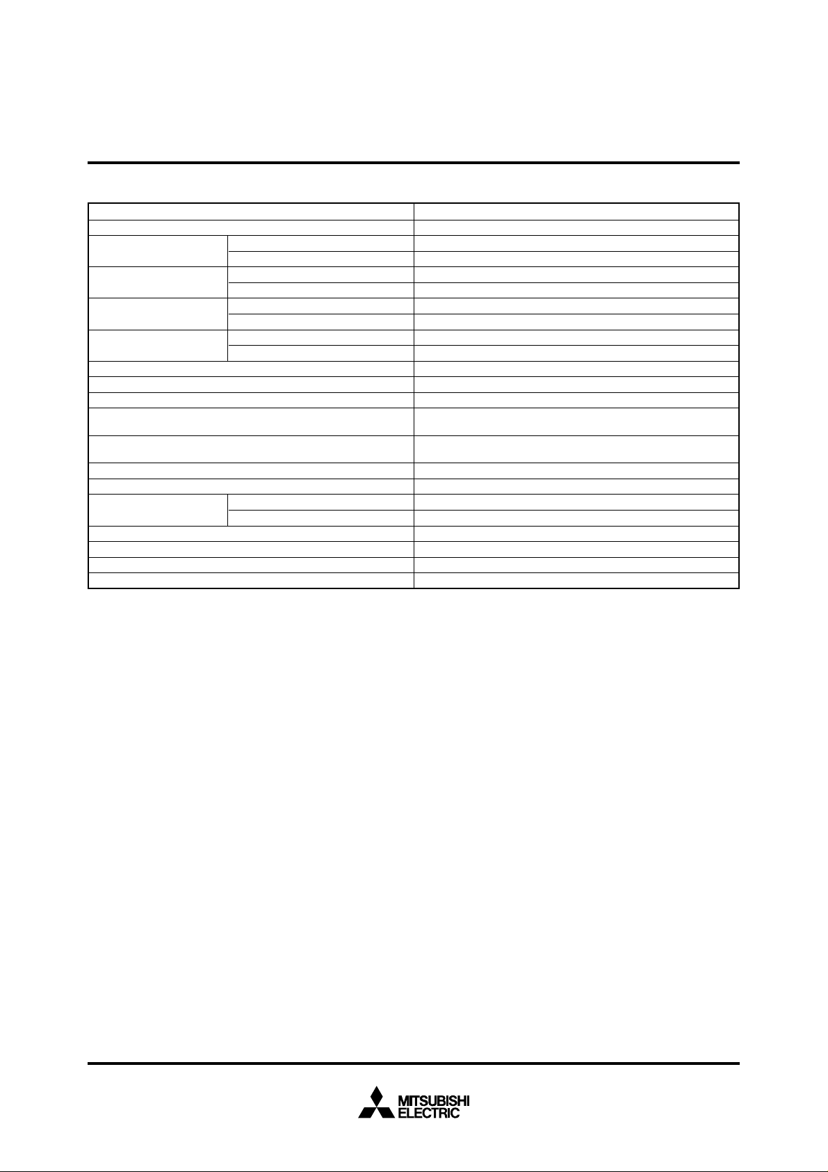
FUNCTIONS OF M37702M2AXXXFP
Number of basic instructions
Instruction execution time
Memory size
Input/Output ports
Multi-function timers
Serial I/O
A-D converter
Watchdog timer
Interrupts
Clock generating circuit
Supply voltage
Power dissipation
Input/Output characteristic
Memory expansion
Operating temperature range
Device structure
Package
Parameter
M37702M2AXXXFP, M37702S1AFP
M37702M2BXXXFP, M37702S1BFP
ROM
RAM
P0 – P2, P4 – P8
P3
TA0, TA1, TA2, TA3, TA4
TB0, TB1, TB2
Input/Output voltage
Output current
103
250 ns (the fastest instruction at external clock 16 MHz frequency)
160 ns (the fastest instruction at external clock 25 MHz frequency)
16 K bytes
512 bytes
8-bit ✕ 8
4-bit ✕ 1
16-bit ✕ 5
16-bit ✕ 3
(UART or clock synchronous serial I/O) ✕ 2
8-bit ✕ 1 (8 channels)
12-bit ✕ 1
3 external types, 16 internal types
(Each interrupt can be set the priority levels to 0 – 7.)
Built-in (externally connected to a ceramic resonator or quartz
crystal resonator)
5 V ± 10%
60 mW (at external clock 16 MHz frequency)
5 V
5 mA
Maximum 16 M bytes
–20 – 85°C
CMOS high-performance silicon gate process
80-pin plastic molded QFP
Functions
3

MITSUBISHI MICROCOMPUTERS
M37702M2AXXXFP, M37702M2BXXXFP
M37702S1AFP, M37702S1BFP
SINGLE-CHIP 16-BIT CMOS MICROCOMPUTER
PIN DESCRIPTION
Pin
VCC, VSS
CNVSS
______
RESET
X
IN
XOUT
_
E
BYTE
CC,
AV
AV
SS
VREF
P00 – P07
P10 – P17
P20 – P27
P30 – P37
P40 – P47
P50 – P57
P60 – P67
P70 – P77
P80 – P87
Name
Power supply
CNVSS input
Reset input
Clock input
Clock output
Enable output
Bus width selection
input
Analog supply input
Reference voltage
input
I/O port P0
I/O port P1
I/O port P2
I/O port P3
I/O port P4
I/O port P5
I/O port P6
I/O port P7
I/O port P8
Input/Output
Input
Input
Input
Output
Output
Input
Input
I/O
I/O
I/O
I/O
I/O
I/O
I/O
I/O
I/O
Functions
Supply 5 V ± 10% to VCC and 0V to VSS.
This pin controls the processor mode. Connect to VSS for single-chip mode, and
CC for external ROM types.
to V
To enter the reset state, this pin must be kept at a “L” condition which should be
maintained for the required time.
These are I/O pins of internal clock generating circuit. Connect a ceramic or quartz
IN
and X
OUT
crystal resonator between X
source should be connected to the X
. When an external clock is used, the clock
IN
pin and the X
OUT
pin should be left open.
Data or instruction read and data write are performed when output from this pin
is “L”.
In memory expansion mode or microprocessor mode, this pin determines
whether the external data bus is 8-bit width or 16-bit width. The width is 16 bits
when “L” signal inputs and 8 bits when “H” signal inputs.
Power supply for the A-D converter. Connect AV
CC to VCC and AVSS to VSS
externally.
This is reference voltage input pin for the A-D converter.
In single-chip mode, port P0 becomes an 8-bit I/O port. An I/O direction register
is available so that each pin can be programmed for input or output. These ports
are in input mode when reset.
Address (A7 – A0) is output in memory expansion mode or microprocessor mode.
In single-chip mode, these pins have the same functions as port P0. When the
BYTE pin is set to “L” in memory expansion mode or microprocessor mode and
external data bus is 16-bit width, high-order data (D15 – D8) is input or output
__
when E output is “L” and an address (A15 – A8) is output when E output is “H”.
If the BYTE pin is “H” that is an external data bus is 8-bit width, only address
(A15 – A8) is output.
In single-chip mode, these pins have the same functions as port P0. In memory
expansion mode or microprocessor mode low-order data (D
output when E output is “L” and an address (A23 – A16) is output when E output
__
7 – D0) is input or
is “H”.
In single-chip mode, these pins have the same functions as port P0. In memory
expansion mode or microprocessor mode, R/W, BHE, ALE and HLDA signals
__ ____
_____
are output.
In single-chip mode, these pins have the same functions as port P0. In memory
expansion mode or microprocessor mode, P40 and P41 become HOLD and RDY
_____
____
input pin respectively. Functions of other pins are the same as in single-chip
mode. In single-chip mode or memory expansion mode, port P42 can be programmed for φ
mode. P4
1 output pin divided the clock to XIN pin by 2. In microprocessor
2 always has the function as φ1 output pin.
In addition to having the same functions as port P0 in single-chip mode, these
pins also function as I/O pins for timer A0, timer A1, timer A2 and timer A3.
In addition to having the same functions as port P0 in single-chip mode, these
pins also function as I/O pins for timer A4, external interrupt input INT0, INT1 and
____
INT2 pins, and input pins for timer B0, timer B1 and timer B2.
____ ____
In addition to having the same functions as port P0 in single-chip mode, these
pins also function as analog input AN
0 – AN7 input pins. P77 also has an A-D
conversion trigger input function.
In addition to having the same functions as port P0 in single-chip mode, these
pins also function as RXD, TXD, CLK, CTS/RTS pins for UART 0 and UART 1.
____ ____
4
MITSUBISHI MICROCOMPUTERS
M37702M2AXXXFP, M37702M2BXXXFP
M37702S1AFP, M37702S1BFP
SINGLE-CHIP 16-BIT CMOS MICROCOMPUTER
BASIC FUNCTION BLOCKS
The M37702M2AXXXFP contains the following devices on a
single chip: ROM and RAM for storing instructions and data, CPU
for processing, bus interface unit (which controls instruction
prefetch and data read/write between CPU and memory), timers,
UART, A-D converter, and other peripheral devices such as I/O
ports. Each of these devices are described below.
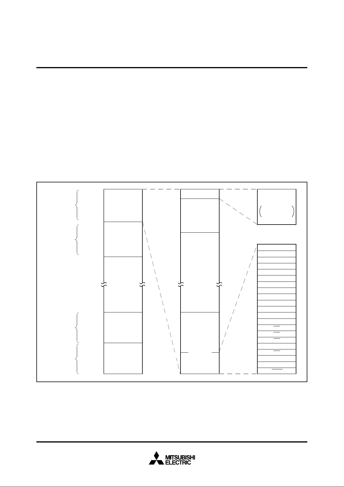
MEMORY
The memory map is shown in Figure 1. The address space is 16
M bytes from addresses 0
divided into 64 K bytes units called banks. The banks are numbered from 0
16 to FF16.
Built-in ROM, RAM and control registers for built-in peripheral devices are assigned to bank 0
Bank 0
16
Bank 1
16
• • • • • • • • • •
Bank FE
16
Bank FF
16
16 to FFFFFF16. The address space is
16.
000000
16
00FFFF
16
010000
16
01FFFF
16
FE0000
16
FEFFFF
16
FF0000
16
FFFFFF
16
000000
00007F
000080
00027F
00C000
00FFD6
00FFFF
The 16 K bytes area from addresses C000
built-in ROM. Addresses FFD6
16 to FFFF16 are the RESET and
16 to FFFF16 is the
interrupt vector addresses and contain the interrupt vectors. Refer
to the section on interrupts for details.
The 512 bytes area from addresses 80
16 to 27F16 contains the
built-in RAM. In addition to storing data, the RAM is used as stack
during a subroutine call, or interrupts.
Assigned to addresses 0
16 to 7F16 are peripheral devices such as
I/O ports, A-D converter, UART, timer, and interrupt control registers.
A 256 bytes direct page area can be allocated anywhere in bank
0
16 using the direct page register DPR. In direct page addressing
mode, the memory in the direct page area can be accessed with
two words thus reducing program steps.
16
16
16
16
Internal RAM
512 bytes
000000
00007F
16
Peripheral devices
control registers
see Fig. 2 for
further information
16
Interrupt vector table
00FFD6
16
A-D conversion
UART1 transmission
UART1 receive
UART0 transmission
UART0 receive
Timer B2
Timer B1
Timer B0
Timer A4
Timer A3
Timer A2
16
16
16
Internal ROM
16K bytes
00FFFE
16
Timer A1
Timer A0
INT
2
INT
1
INT
0
Watchdog timer
DBC
BRK instruction
Zero divide
RESET
Fig. 1 Memory map
5
MITSUBISHI MICROCOMPUTERS
M37702M2AXXXFP, M37702M2BXXXFP
M37702S1AFP, M37702S1BFP
SINGLE-CHIP 16-BIT CMOS MICROCOMPUTER
Address (Hexadecimal notation)
000000
000001
000002
000003
000004
000005
000006
000007
000008
000009
00000A
00000B
00000C
00000D
00000E
00000F
000010
000011
000012
Port P0
Port P1
Port P0 data direction register
Port P1 data direction register
Port P2
Port P3
Port P2 data direction register
Port P3 data direction register
Port P4
Port P5
Port P4 data direction register
Port P5 data direction register
Port P6
Port P7
Port P6 data direction register
Port P7 data direction register
Port P8
000013
000014
Port P8 data direction register
000015
000016
000017
000018
000019
00001A
00001B
00001C
00001D
00001E
00001F
000020
A-D control register
A-D sweep pin selection register
A-D register 0
000021
000022
A-D register 1
000023
000024
A-D register 2
000025
000026
A-D register 3
000027
000028
A-D register 4
000029
00002A
A-D register 5
00002B
00002C
A-D register 6
00002D
00002E
A-D register 7
00002F
000030
000031
000032
000033
000034
000035
000036
000037
000038
000039
00003A
00003B
00003C
00003D
00003E
00003F
UART 0 transmit/receive mode register
UART 0 bit rate generator
UART 0 transmission buffer register
UART 0 transmit/receive control register 0
UART 0 transmit/receive control register 1
UART 0 receive buffer register
UART 1 transmit/receive mode register
UART 1 bit rate generator
UART 1 transmission buffer register
UART 1 transmit/receive control register 0
UART 1 transmit/receive control register 1
UART 1 receive buffer register
Address (Hexadecimal notation)
000040
Count start flag
000041
000042
One-shot start flag
000043
000044
Up-down flag
000045
000046
000047
000048
000049
00004A
00004B
00004C
00004D
00004E
00004F
000050
000051
000052
000053
000054
000055
000056
000057
000058
000059
00005A
00005B
00005C
00005D
00005E
Timer A0
Timer A1
Timer A2
Timer A3
Timer A4
Timer B0
Timer B1
Timer B2
Timer A0 mode register
Timer A1 mode register
Timer A2 mode register
Timer A3 mode register
Timer A4 mode register
Timer B0 mode register
Timer B1 mode register
Timer B2 mode register
Processor mode register
00005F
000060
000061
Watchdog timer
Watchdog timer frequency selection flag
000062
000063
000064
000065
000066
000067
000068
000069
00006A
00006B
00006C
00006D
00006E
00006F
000070
000071
000072
000073
000074
000075
000076
000077
000078
000079
00007A
00007B
00007C
00007D
00007E
00007F
A-D conversion interrupt control register
UART 0 transmission interrupt control register
UART 0 receive interrupt control register
UART 1 transmission interrupt control register
UART 1 receive interrupt control register
Timer A0 interrupt control register
Timer A1 interrupt control register
Timer A2 interrupt control register
Timer A3 interrupt control register
Timer A4 interrupt control register
Timer B0 interrupt control register
Timer B1 interrupt control register
Timer B2 interrupt control register
INT
0
interrupt control register
INT
1
interrupt control register
INT
2
interrupt control register
Fig. 2 Location of peripheral devices and interrupt control registers
6
MITSUBISHI MICROCOMPUTERS
M37702M2AXXXFP, M37702M2BXXXFP
M37702S1AFP, M37702S1BFP
SINGLE-CHIP 16-BIT CMOS MICROCOMPUTER
CENTRAL PROCESSING UNIT (CPU)
The CPU has ten registers and is shown in Figure 3. Each of
these registers is described below.
ACCUMULATOR A (A)
Accumulator A is the main register of the microcomputer. It consists of 16 bits and the lower 8 bits can be used separately. The
data length flag m determines whether the register is used as 16bit register or as 8-bit register. It is used as a 16-bit register when
flag m is “0” and as an 8-bit register when flag m is “1”. Flag m is
a part of the processor status register (PS) which is described
later.
Data operations such as calculations, data transfer, input/output,
etc., is executed mainly through the accumulator.
ACCUMULATOR B (B)
Accumulator B has the same functions as accumulator A, but the
use of accumulator B requires more instruction bytes and execution cycles than accumulator A.
INDEX REGISTER X (X)
Index register X consists of 16 bits and the lower 8 bits can be
used separately. The index register length flag x determines
whether the register is used as 16-bit register or as 8-bit register.
It is used as a 16-bit register when flag x is “0” and as an 8-bit reg-
ister when flag x is “1”. Flag x is a part of the processor status register (PS) which is described later.
In index addressing mode, register X is used as the index register
and the contents of this address is added to obtain the real address.
Also, when executing a block transfer instruction MVP or MVN, the
contents of index register X indicate the low-order 16 bits of the
source data address. The third byte of the MVP and MVN is the
high-order 8 bits of the source data address.
INDEX REGISTER Y (Y)
Index register Y consists of 16 bits and the lower 8 bits can be
used separately. The index register length flag x determines
whether the register is used as 16-bit register or as 8-bit register.
It is used as a 16-bit register when flag x is “0” and as an 8-bit register when flag x is “1”. Flag x is a part of the processor status
register (PS) which is described later.
In index addressing mode, register Y is used as the index register
and the contents of this address is added to obtain the real address.
Also, when executing a block transfer instruction MVP or MVN, the
contents of index register Y indicate the low-order 16 bits of the
destination address. The second byte of the MVP and MVN is the
high-order 8 bits of the destination data address.
70
PG
70
DT
Program bank register PG
Data bank register DT
Fig. 3 Register structure
15 07
15 07
15 07
15 07
15 0
A
H
B
H
X
H
Y
H
A
L
B
L
X
L
Y
L
S
15 0
PC
15 0
DPR
715 0
IPL
N
0
1
IPL2IPL
Accumulator A
Accumulator B
Index register X
Index register Y
Stack pointer S
Program counter PC
Direct page register DPR
Processor status register PS0
CZIDxmV0000
Carry flag
Zero flag
Interrupt disable flag
Decimal mode flag
Index register length flag
Data length flag
Overflow flag
Negative flag
Processor interrupt priority level IPL
7

MITSUBISHI MICROCOMPUTERS
M37702M2AXXXFP, M37702M2BXXXFP
M37702S1AFP, M37702S1BFP
SINGLE-CHIP 16-BIT CMOS MICROCOMPUTER
STACK POINTER (S)
Stack pointer (S) is a 16-bit register. It is used during a subroutine
call or interrupts. It is also used during stack, stack pointer relative, or stack pointer relative indirect indexed Y addressing mode.
PROGRAM COUNTER (PC)
Program counter (PC) is a 16-bit counter that indicates the low-order 16-bits of the next program memory address to be executed.
There is a bus interface unit between the program memory and
the CPU, so that the program memory is accessed through bus interface unit. This is described later.
PROGRAM BANK REGISTER (PG)
Program bank register is an 8-bit register that indicates the highorder 8 bits of the next program memory address to be executed.
When a carry occurs by incrementing the contents of the program
counter, the contents of the program bank register (PG) is
incremented by 1. Also, when a carry or borrow occurs after adding or subtracting the offset value to or from the contents of the
program counter (PC) using branch instruction, the contents of the
program bank register (PG) is incremented or decremented by 1
so that programs can be written without worrying about bank
boundaries.
DATA BANK REGISTER (DT)
Data bank register (DT) is an 8-bit register. With some addressing
modes, a part of the data bank register (DT) is used to specify a
memory address. The contents of data bank register (DT) is used
as the high-order 8 bits of a 24-bit address. Addressing modes
that use the data bank register (DT) are direct indirect, direct indexed X indirect, direct indirect indexed Y, absolute, absolute bit,
absolute indexed X, absolute indexed Y, absolute bit relative, and
stack pointer relative indirect indexed Y.
DIRECT PAGE REGISTER (DPR)
Direct page register (DPR) is a 16-bit register. Its contents is used
as the base address of a 256-byte direct page area. The direct
page area is allocated in bank 0, but when the contents of DPR is
FF01
16 or greater, the direct page area spans across bank 016 and
bank 1
16. All direct addressing modes use the contents of the di-
rect page register (DPR) to generate the data address. If the
low-order 8 bits of the direct page register (DPR) is “00
number of cycles required to generate an address is minimized.
Normally the low-order 8 bits of the direct page register (DPR) is
set to “00
16”.
16”, the
PROCESSOR STATUS REGISTER (PS)
Processor status register (PS) is an 11-bit register. It consists of a
flag to indicate the result of operation and CPU interrupt levels.
Branch operations can be performed by testing the flags C, Z, V,
and N.
The details of each processor status register bit are described
below.
1. Carry flag (C)
The carry flag contains the carry or borrow generated by the ALU
after an arithmetic operation. This flag is also affected by shift and
rotate instructions. This flag can be set and reset directly with the
SEC and CLC instructions or with the SEP and CLP instructions.
2. Zero flag (Z)
This zero flag is set if the result of an arithmetic operation or data
transfer is zero and reset if it is not. This flag can be set and reset directly with the SEP and CLP instructions.
3. Interrupt disable flag (I)
When the interrupt disable flag is set to “1”, all interrupts except
watchdog timer, DBC, and software interrupt are disabled. This
flag is set to “1” automatically when there is an interrupt. It can be
set and reset directly with the SEI and CLI instructions or SEP and
CLP instructions.
____
4. Decimal mode flag (D)
The decimal mode flag determines whether addition and subtraction are performed as binary or decimal. Binary arithmetic is
performed when this flag is “0”. If it is “1”, decimal arithmetic is
performed with each word treated as two or four digit decimal.
Arithmetic operation is performed using four digits when the data
length flag m is “0” and with two digits when it is “1”. (Decimal operation is possible only with the ADC and SBC instructions.) This
flag can be set and reset with the SEP and CLP instructions.
8
MITSUBISHI MICROCOMPUTERS
M37702M2AXXXFP, M37702M2BXXXFP
M37702S1AFP, M37702S1BFP
SINGLE-CHIP 16-BIT CMOS MICROCOMPUTER
5. Index register length flag (x)
The index register length flag determines whether index register X
and index register Y are used as 16-bit registers or as 8-bit registers. The registers are used as 16-bit registers when flag x is “0”
and as 8-bit registers when it is “1”. This flag can be set and reset
with the SEP and CLP instructions.
6. Data length flag (m)
The data length flag determines whether the data length is 16-bit
or 8-bit. The data length is 16-bit when flag m is “0” and 8-bit when
it is “1”. This flag can be set and reset with the SEM and CLM instructions or with the SEP and CLP instructions.
7. Overflow flag (V)
The overflow flag has meaning when addition or subtraction is
performed a word as signed binary number. When the data length
flag m is “0”, the overflow flag is set when the result of addition or
subtraction is outside the range between –32768 and +32767.
When the data length flag m is “1”, the overflow flag is set when
the result of addition or subtraction is outside the range between
–128 and +127. It is reset in all other cases. The overflow flag can
also be set and reset directly with the SEP, and CLV or CLP instructions.
8. Negative flag (N)
The negative flag is set when the result of arithmetic operation or
data transfer is negative (If data length flag m is “0”, when data bit
15 is “1”. If data length flag m is “1”, when data bit 7 is “1”.) It is reset in all other cases. It can also be set and reset with the SEP
and CLP instructions.
9. Processor interrupt priority level (IPL)
The processor interrupt priority level (IPL) consists of 3 bits and
determines the priority of processor interrupts from level 0 to level
7. Interrupt is enabled when the interrupt priority of the device requesting interrupt (set using the interrupt control register) is higher
than the processor interrupt priority. When interrupt is enabled, the
current processor interrupt priority level is saved in a stack and the
processor interrupt priority level is replaced by the interrupt priority level of the device requesting the interrupt. Refer to the section
on interrupts for more details.
BUS INTERFACE UNIT
The CPU operates on an internal clock frequency which is obtained by dividing the external clock frequency f(X
frequency is twice the bus cycle frequency. In order to speed-up
processing, a bus interface unit is used to pre-fetch instructions
when the data bus is idle. The bus interface unit synchronizes the
CPU and the bus and pre-fetches instructions. Figure 4 shows the
relationship between the CPU and the bus interface unit. The bus
interface unit has a program address register, a 3-byte instruction
queue buffer, a data address register, and a 2-byte data buffer.
The bus interface unit obtains an instruction code from memory
and stores it in the instruction queue buffer, obtains data from
memory and stores it in the data buffer, or writes the data from the
data buffer to the memory.
IN) by two. This
D'
15 to D'8
D'7 to D'
0
A'
23
to A'
0
CPU
Control signal
Fig. 4 Relationship between the CPU and the bus interface unit
Bus interface
unit
D
15
to D
D7 to D
A
23
to A
BHE
R/
W
E
ALE
BYTE
HOLD
8
0
0
9
MITSUBISHI MICROCOMPUTERS
M37702M2AXXXFP, M37702M2BXXXFP
M37702S1AFP, M37702S1BFP
SINGLE-CHIP 16-BIT CMOS MICROCOMPUTER
The bus interface unit operates using one of the waveforms (1) to
(6) shown in Figure 5. The standard waveforms are (1) and (2).
The ALE signal is used to latch only the address signal from the
multiplexed signal containing data and address.
_
The E signal becomes “L” when the bus interface unit reads an instruction code or data from memory or when it writes data to
memory. Whether to perform read or write is controlled by the R/W
signal. Read is performed when the R/W signal is “H” state and
__
__
write is performed when it is “L” state.
Waveform (1) in Figure 5 is used to access a single byte or two
bytes simultaneously. To read or wr ite two bytes simultaneously,
the first address accessed must be even. Furthermore, when accessing an external memory area in memory expansion mode or
microprocessor mode, set the bus width selection input pin BYTE
to “L”. (external data bus width to 16 bits) The internal memory
area is always treated as 16-bit bus width regardless of BYTE.
When performing 16-bit data read or write, if the conditions for simultaneously accessing two bytes are not satisfied, waveform (2)
is used to access each byte one by one.
However, when prefetching the instruction code, if the address of
the instruction code is odd, waveform (1) is used, and only one
byte is read in the instruction queue buffer.
The signals A0 and BHE in Figure 5 are used to control these
____
cases: 1-byte read from even address, 1-byte read from odd address, 2-byte simultaneous read from even and odd addresses,
1-byte write to even address, 1-byte write to odd address, or 2byte simultaneous write to even and odd addresses. The A
that is the address bit 0 is “L” when an even number address is
accessed. The BHE signal becomes “L” when an odd number ad-
____
0 signal
dress is accessed.
The bit 2 of processor mode register (address 5E
When this bit is set to “0”, the “L” width of E signal is 2 times as
16) is the wait bit.
_
long when accessing an external memory area in memory expansion mode or microprocessor mode. However, the “L” width of E
signal is not extended when an internal memory area is accessed.
When the wait bit is “1”, the “L” width of E signal is not extended
_
for any access. Waveform (3) is an expansion of the “L” width of E
signal in waveform (1). Waveform (4), (5), and (6) are expansion
of each “L” width of E signal in waveform (2), first half of waveform
_
(2), and the last half of waveform (2) respectively.
Instruction code read, data read, and data write are described below.
_
_
Internal clock φ
(1)
Port P2
E
AD
ALE
A + 1
AD D
(2)
Port P2
E
ALE
AD
(3)
Port P2
E
ALE
A + 1
DD
(4)
Port P2
A
E
ALE
A + 1
DD
(5)
Port P2
A
E
ALE
A + 1
AD D
(6)
Port P2
E
ALE
A : Address
D : Data
These waveforms are at the memory expansion mode and
the microprocessor mode.
10
Access
Access 2-byte
method
A
BHE
0
____
simultaneously
“L” “L” “H”
“L” “H” “L”
Signal
Fig. 5 Relationship between access method and signals A0
and BHE
Access even
address 1-byte
Access odd
address 1-byte

MITSUBISHI MICROCOMPUTERS
M37702M2AXXXFP, M37702M2BXXXFP
M37702S1AFP, M37702S1BFP
SINGLE-CHIP 16-BIT CMOS MICROCOMPUTER
Instruction code read will be described first.
The CPU obtains instruction codes from the instruction queue
buffer and executes them. The CPU notifies the bus interface unit
that it is requesting an instruction code during an instruction code
request cycle. If the requested instruction code is not yet stored in
the instruction queue buffer, the bus interface unit halts the CPU
until it can store more instructions than requested in the instruction
queue buffer.
Even if there is no instruction code request from the CPU, the bus
interface unit reads instruction codes from memory and stores
them in the instruction queue buffer when the instruction queue
buffer is empty or when only one instruction code is stored and the
bus is idle on the next cycle.
This is referred to as instruction pre-fetching.
Normally, when reading an instruction code from memory, if the
accessed address is even the next odd address is read together
with the instruction code and stored in the instruction queue buffer.
However, in memory expansion mode or microprocessor mode, if
the bus width switching pin BYTE is “H”, external data bus width is
8 bits and the address to be read is in external memory area is
odd, only one byte is read and stored in the instruction queue
buffer. Therefore, waveform (1) or (3) in Figure 5 is used for instruction code read.
Data read and write are described below.
The CPU notifies the bus interface unit when performing data read
or write. At this time, the bus interface unit halts the CPU if the bus
interface unit is already using the bus or if there is a request with
higher priority. When data read or write is enabled, the bus interface unit uses one of the waveforms from (1) to (6) in Figure 5 to
perform the operation.
During data read, the CPU waits until the entire data is stored in
the data buffer. The bus interface unit sends the address received
from the CPU to the address bus. Then it reads the memory when
_
the E signal is “L” and stores the result in the data buffer.
During data write, the CPU writes the data in the data buffer and
the bus interface unit writes it to memory. Therefore, the CPU can
proceed to the next step without waiting for write to complete. The
bus interface unit sends the address received from the CPU to the
address bus. Then when the E signal is “L”, the bus interface unit
sends the data in the data buffer to the data bus and writes it to
memory.
_
11
MITSUBISHI MICROCOMPUTERS
M37702M2AXXXFP, M37702M2BXXXFP
M37702S1AFP, M37702S1BFP
SINGLE-CHIP 16-BIT CMOS MICROCOMPUTER
INTERRUPTS
Table 1 shows the interrupt types and the corresponding interrupt
vector addresses. Reset is also treated as a type of interrupt and
is discussed in this section, too. DBC is an interrupt used during
debugging.
Interrupts other than reset, DBC, watchdog timer, zero divide, and
BRK instruction all have interrupt control registers. Table 2 shows
the addresses of the interrupt control registers and Figure 6 shows
the bit configuration of the interrupt control register.
Use the SEB and CLB instructions when setting each interrupt
control register.
The interrupt request bit is automatically cleared by the hardware
during reset or when processing an interrupt.
Also, interrupt request bits other than DBC and watchdog timer
can be cleared by software.
____ ____
INT2 to INT0 are external interrupts and whether to cause an interrupt at the input level (level sense) or at the edge (edge sense)
can be selected with the level sense/edge sense selection bit. Furthermore, the polarity of the interrupt input can be selected with
polarity selection bit.
Timer and UART interrupts are described in the respective section. The priority of interrupts when multiple interrupts are caused
simultaneously is partially fixed by hardware, but, it can also be
adjusted by software as shown in Figure 7. The hardware priority
is fixed the following:
____
reset > DBC > watchdog timer > other interrupts
____
____
____
Table 1. Interrupt types and the interrupt vector addresses
Interrupts
A-D conversion
UART1 transmit
UART1 receive
UART0 transmit
UART0 receive
Timer B2
Timer B1
Timer B0
Timer A4
Timer A3
Timer A2
Timer A1
Timer A0
____
INT2 external interrupt
____
INT1 external interrupt
____
INT0 external interrupt
Watchdog timer
____
DBC (unusable)
Break instruction
Zero divide
Reset
Vector addresses
00FFD616 00FFD716
00FFD816 00FFD916
00FFDA16 00FFDB16
00FFDC16 00FFDD16
00FFDE16 00FFDF16
00FFE016 00FFE116
00FFE216 00FFE316
00FFE416 00FFE516
00FFE616 00FFE716
00FFE816 00FFE916
00FFEA16 00FFEB16
00FFEC16 00FFED16
00FFEE16 00FFEF16
00FFF016 00FFF116
00FFF216 00FFF316
00FFF416 00FFF516
00FFF616 00FFF716
00FFF816 00FFF916
00FFFA16 00FFFB16
00FFFC16 00FFFD16
00FFFE16 00FFFF16
7
6543210
Interrupt control register configuration for A-D converter, UART0, UART1, timer A0 to timer A4, and
timer B0 to timer B2
7
6543210
Interrupt control register configuration for
Fig. 6 Interrupt control register configuration
Interrupt priority
Interrupt request bit
0 : No interrupt
1 : Interrupt
Interrupt priority
Interrupt request bit
0 : No interrupt
1 : Interrupt
Polarity selection bit
0 : Set interrupt request bit at “H” level for level sense and when changing
from “H” to “L” level for edge sense.
1 : Set interrupt request bit at “L” level for level sense and when changing
from “L” to “H” level for edge sense.
Level sense/edge sense selection bit
0 : Edge sense
1 : Level sense
INT
2
to
INT
0.
12
MITSUBISHI MICROCOMPUTERS
M37702M2AXXXFP, M37702M2BXXXFP
M37702S1AFP, M37702S1BFP
SINGLE-CHIP 16-BIT CMOS MICROCOMPUTER
Table 2. Addresses of interrupt control registers
Interrupt control registers
A-D conversion interrupt control register
UART0 transmit interrupt control register
UART0 receive interrupt control register
UART1 transmit interrupt control register
UART1 receive interrupt control register
Timer A0 interrupt control register
Timer A1 interrupt control register
Timer A2 interrupt control register
Timer A3 interrupt control register
Timer A4 interrupt control register
Timer B0 interrupt control register
Timer B1 interrupt control register
Timer B2 interrupt control register
____
INT0 interrupt control register
____
INT1 interrupt control register
____
INT2 interrupt control register
Addresses
00007016
00007116
00007216
00007316
00007416
00007516
00007616
00007716
00007816
00007916
00007A16
00007B16
00007C16
00007D16
00007E16
00007F16
Interrupts caused by a BRK instruction and when dividing by zero
are software interrupts and are not included in this list.
Other interrupts previously mentioned are A-D converter, UART,
Timer, INT interrupts. The priority of these interrupts can be
changed by changing the priority level in the corresponding interrupt control register by software.
Figure 8 shows a diagram of the interrupt priority resolution circuit.
When an interrupt is caused, the each interrupt device compares
its own priority with the priority from above and if its own priority is
higher, then it sends the priority below and requests the interrupt.
If the priorities are the same, the one above has priority.
This comparison is repeated to select the interrupt with the highest
priority among the interrupts that are being requested. Finally the
selected interrupt is compared with the processor interrupt priority
level (IPL) contained in the processor status register (PS) and the
request is accepted if it is higher than IPL and the interrupt disable
flag I is “0”. The request is not accepted if flag I is “1”. The reset,
____
DBC, and watchdog timer interrupts are not affected by the interrupt disable flag I.
When an interrupt is accepted, the contents of the processor status register (PS) is saved to the stack and the interrupt disable
flag I is set to “1”.
Furthermore, the interrupt request bit of the accepted interrupt is
cleared to “0” and the processor interrupt priority level (IPL) in the
processor status register (PS) is replaced by the priority level of
the accepted interrupt.
Therefore, multi-level priority interrupts are possible by resetting
the interrupt disable flag I to “0” and enable further interrupts.
For reset, DBC, watchdog timer, zero divide, and BRK instruction
____
interrupts, which do not have an interrupt control register, the processor interrupt level (IPL) is set as shown in Table 3.
Priority resolution is performed by latching the interrupt request bit
and interrupt priority level so that they do not change. They are
sampled at the first half and latched at the last half of the operation code fetch cycle.
Because priority resolution takes some time, no sampling pulse is
generated for a certain interval even if it is the next operation code
fetch cycle.
Priority is determined by hardware
3
4
➂➃
Watchdog
timer
DBC
12
Reset
A-D converter, UART, Timer, INT interrupts
Priority can be changed with software inside
4
Fig. 7 Interrupt priority
Level 0
A-D conversion
Interrupt request
Reset
DBC
Watchdog
timer
Interrupt disable flag I
IPL
UART1 transmit
UART1 receive
UART0 transmit
UART0 receive
Timer B2
Timer B1
Timer B0
Timer A4
Timer A3
Timer A2
Timer A1
Timer A0
INT
2
INT
1
INT
0
Fig. 8 Interrupt priority resolution
13
MITSUBISHI MICROCOMPUTERS
M37702M2AXXXFP, M37702M2BXXXFP
M37702S1AFP, M37702S1BFP
SINGLE-CHIP 16-BIT CMOS MICROCOMPUTER
As shown in Figure 9, there are three different interrupt priority
resolution time from which one is selected by software. After the
selected time has elapsed, the highest priority is determined and
is processed after the currently executing instruction has been
completed.
The time is selected with bits 4 and 5 of the processor mode register (address 5E
16) shown in Figure 10. Table 4 shows the
relationship between these bits and the number of cycles. After a
reset, the processor mode register is initialized to “00
16” and
therefore, the longest time is selected.
However, the shortest time should be selected by software.
Internal clock
Operation code fetch cycle
Sampling pulse
Priority resolution time
φ
0
Table 3. Value set in processor interrupt level (IPL) during an
interrupt
Interrupt types
Reset
____
DBC
Watchdog timer
Zero divide
BRK instruction
Setting value
0
7
7
Not change value of IPL.
Not change value of IPL.
Table 4. Relationship between priority level resolution time
selection bit and number of cycles
Priority level resolution time selection bit
Bit 5
0
0
1
Bit 4
0
1
0
Number of cycles
7 cycles of φ
4 cycles of φ
2 cycles of φ
φ : internal clock
Select from 0 to 2 with bits
4 and 5 of the processor
mode register
Fig. 9 Interrupt priority resolution time
7
6 5 4 3 2 1 0
0
Fig. 10 Processor mode register configuration
1
2
Processor mode register (5E16)
Processor mode bits
0 0 : Single-chip mode
0 1 : Memory expansion mode
1 0 : Microprocessor mode
1 1 : Evaluation chip mode
Wait bit
0 : Wait
1 : No wait
Software reset bit
The processor is reset when this bit is set to “1”.
Priority resolution time selection bits
0 0 : Select 0 in Figure 9
0 1 : Select 1 in Figure 9
1 0 : Select 2 in Figure 9
Test mode bit
Must be “0”
Clock
φ
1
output selection bit
φ
1
φ
1
output
output
0 : No
1 :
14
MITSUBISHI MICROCOMPUTERS
M37702M2AXXXFP, M37702M2BXXXFP
M37702S1AFP, M37702S1BFP
SINGLE-CHIP 16-BIT CMOS MICROCOMPUTER
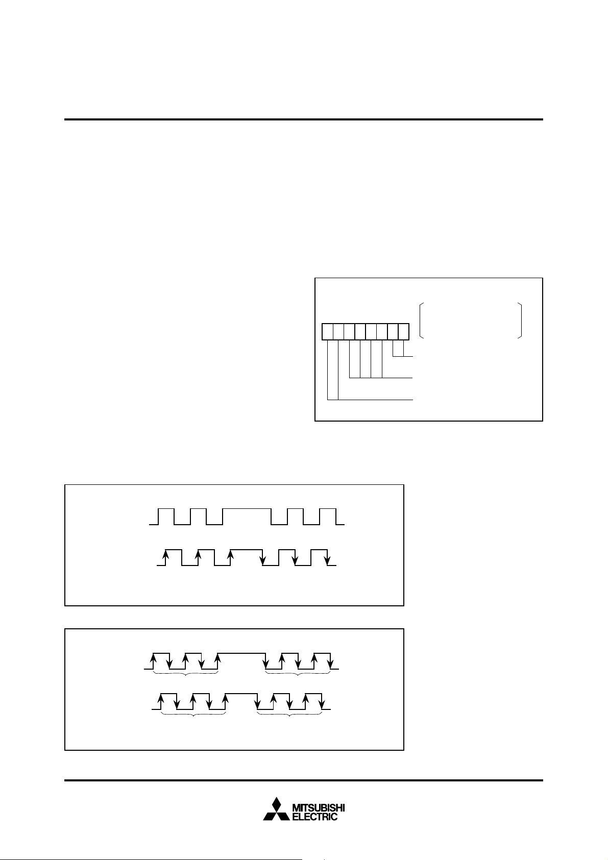
TIMER
There are eight 16-bit timers. They are divided by type into timer A
(5) and timer B (3).
The timer I/O pins are shared with I/O pins for port P5 and P6. To
use these pins as timer input pins, the data direction register bit
corresponding to the pin must be cleared to “0” to specify input
mode.
TIMER A
Figure 11 shows a block diagram of timer A.
Timer A has four modes; timer mode, event counter mode, oneshot pulse mode, and pulse width modulation mode. The mode is
selected with bits 0 and 1 of the timer Ai mode register (i = 0 to 4).
Each of these modes is described below.
f
f(X
IN
)
Clock source selection
f
2
f
16
f
64
f
512
TAi
(i = 0 – 4)
2
1/2 1/8 1/2 1/2 1/8
Polarity
selection
IN
f
16
• Timer
• One-shot
• Pulse width modulation
Timer (gate function)
Event counter
External trigger
f
32
(1) Timer mode [00]
Figure 12 shows the bit configuration of the timer Ai mode register
during timer mode. Bits 0, 1, and 5 of the timer Ai mode register
must always be “0” in timer mode.
Bit 3 is ignored if bit 4 is “0”.
Bits 6 and 7 are used to select the timer counter source.
The counting of the selected clock starts when the count start flag
is “1” and stops when it is “0”.
Figure 13 shows the bit configuration of the count start flag. The
counter is decremented, an interrupt is caused and the interrupt
request bit in the timer Ai interrupt control register is set when the
contents becomes 0000
reload register is transferred to the counter and count is continued.
f
64
f
Data bus (odd)
Data bus (even)
Reload register(16)
Count start flag
(4016)
Down count
16. At the same time, the contents of the
512
(Lower 8 bits)
(Higher 8 bits)
Counter(16)
Up/Down
Always decremented
except in event count mode
Addresses
Timer A0 4716 46
Timer A1 4916 48
Timer A2 4B16 4A
Timer A3 4D16 4C
Timer A4 4F16 4E
16
16
16
16
16
Pulse output
TAi
OUT
(i = 0 – 4)
Fig. 11 Block diagram of timer A
Up-down flag
(4416)
Toggle flip-flop
15
MITSUBISHI MICROCOMPUTERS
M37702M2AXXXFP, M37702M2BXXXFP
M37702S1AFP, M37702S1BFP
SINGLE-CHIP 16-BIT CMOS MICROCOMPUTER
When bit 2 of the timer Ai mode register is “1”, the output is generated from TAi
of the counter reaches to 0000
start flag is “0”, “L” is output from TAi
When bit 2 is “0”, TAi
bit 4 is “0”, TAi
OUT pin. The output is toggled each time the contents
16. When the contents of the count
OUT pin.
OUT can be used as a normal port pin. When
IN can be used as a normal port pin. When bit 4 is
“1”, counting is performed only while the input signal from the
TAi
IN pin is “H” or “L” as shown in Figure 14. Therefore, this can
be used to measure the pulse width of the TAi
IN input signal.
Whether to count while the input signal is “H” or while it is “L” is
determined by bit 3. If bit 3 is “1”, counting is performed while the
TAi
IN pin input signal is “H” and if bit 3 is “0”, counting is performed
Timer A0 mode register 56
Timer A1 mode register 57
Timer A2 mode register 58
623451
70
0
Timer A3 mode register 59
Timer A4 mode register 5A
00
0
0 : Always “00” in timer mode
0 : No pulse output (TAi
1 : Pulse output
while it is “L”.
Note that the duration of “H” or “L” on the TAi
IN pin must be two or
more cycles of the timer count source.
When data is written to timer Ai register with timer Ai halted, the
same data is also written to the reload register and the counter.
When data is written to timer Ai which is busy, the data is written to
the reload register, but not to the counter. The counter is reloaded
with new data from the reload register at the next reload timer. The
contents of the counter can be read at any time.
When the value set in the timer Ai register is n, the timer frequency
dividing ratio is 1/(n + 1).
Addresses
16
16
16
16
16
OUT
is normal port pin)
0 ✕ : No gate function (TAi
1
0 : Count only while TAiIN input is “L”
1 : Count only while TAi
1
0 : Always “0” in timer mode
Clock source selection bit
0 0 : Select f
0 1 : Select f
1 0 : Select f
1 1 : Select f
Fig. 12 Timer Ai mode register bit configuration during timer mode
2
16
64
512
IN
is normal port pin)
IN
input is “H”
16
MITSUBISHI MICROCOMPUTERS
M37702M2AXXXFP, M37702M2BXXXFP
M37702S1AFP, M37702S1BFP
SINGLE-CHIP 16-BIT CMOS MICROCOMPUTER
70654321
Fig. 13 Count start flag bit configuration
Selected clock source f
TAi
i
N
Count start flag
(Stop at “0”, Start at “1”)
Timer A0 count start flag
Timer A1 count start flag
Timer A2 count start flag
Timer A3 count start flag
Timer A4 count start flag
Timer B0 count start flag
Timer B1 count start flag
Timer B2 count start flag
Address
40
16
Timer mode register
Bit 4 Bit 3
10
Timer mode register
Bit 4 Bit 3
11
11
Fig. 14 Count waveform when gate function is available
17
MITSUBISHI MICROCOMPUTERS
M37702M2AXXXFP, M37702M2BXXXFP
M37702S1AFP, M37702S1BFP
SINGLE-CHIP 16-BIT CMOS MICROCOMPUTER
(2) Event counter mode [01]
Figure 15 shows the bit configuration of the timer Ai mode register
during event counter mode. In event counter mode, the bit 0 of the
timer Ai mode register must be “1” and bit 1 and 5 must be “0”.
The input signal from the TAi
IN pin is counted when the count start
flag shown in Figure 13 is “1“ and counting is stopped when it
is “0”.
Count is performed at the fall of the input signal when bit 3 is “0”
and at the rise of the signal when it is “1”.
In event counter mode, whether to increment or decrement the
count can be selected with the up-down flag or the input signal
from the TAi
OUT pin.
When bit 4 of the timer Ai mode register is “0”, the up-down flag is
used to determine whether to increment or decrement the count
(decrement when the flag is “0” and increment when it is “1”). Figure 16 shows the bit configuration of the up-down flag.
When bit 4 of the timer Ai mode register is “1”, the input signal
from the TAi
OUT pin is used to determine whether to increment or
decrement the count. However, note that bit 2 must be “0” if bit 4
is “1” because if bit 2 is “1”, TAi
OUT pin becomes an output pin with
pulse output.
The count is decremented when the input signal from the TAi
OUT
pin is “L” and incremented when it is “H”. Determine the level of
the input signal from the TAi
the TAi
IN pin.
OUT pin before valid edge is input to
An interrupt request signal is generated and the interrupt request
bit in the timer Ai interrupt control register is set when the counter
reaches 0000
16 (decrement count) or FFFF16 (increment count).
At the same time, the contents of the reload register is transferred
to the counter and the count is continued.
When bit 2 is “1” and the counter reaches 0000
count) or FFFF
ity is output from TAi
If bit 2 is “0”, TAi
ever, if bit 4 is “1“ and the TAi
16 (increment count), the waveform reversing polar-
OUT pin.
OUT pin can be used as a normal port pin. How-
OUT pin is used as an output pin, the
16 (decrement
output from the pin changes the count direction. Therefore, bit 4
should be “0” unless the output from the TAi
OUT pin is to be used
to select the count direction.
Timer A0 mode register 56
Timer A1 mode register 57
Timer A2 mode register 58
7 6543210
001
✕✕
Timer A3 mode register 59
Timer A4 mode register 5A
0 1 : Always “01” in event counter
mode
0 : No pulse output
1 : Pulse output
0 : Count at the falling edge of input
signal
1 : Count at the rising edge of input
signal
0 : Increment or decrement according
to up-down flag
1 : Increment or decrement according
to TAi
0 : Always “0” in event counter mode
✕ ✕
OUT
: Not used in event counter mode
Fig. 15 Timer Ai mode register bit configuration during event
counter mode
7 6543210
Up-down flag
Timer A0 up-down flag
Timer A1 up-down flag
Timer A2 up-down flag
Timer A3 up-down flag
Timer A4 up-down flag
Timer A2 two-phase pulse signal processing
selection bit
0 : Two-phase pulse signal processing disabled
1 : Two-phase pulse signal processing mode
Timer A3 two-phase pulse signal processing
selection bit
0 : Two-phase pulse signal processing disabled
1 : Two-phase pulse signal processing mode
Timer A4 two-phase pulse signal processing
selection bit
0 : Two-phase pulse signal processing disabled
1 : Two-phase pulse signal processing mode
Addresses
16
16
16
16
16
pin input signal level
Address
44
16
18
Fig. 16 Up-down flag bit configuration
MITSUBISHI MICROCOMPUTERS
M37702M2AXXXFP, M37702M2BXXXFP
M37702S1AFP, M37702S1BFP
SINGLE-CHIP 16-BIT CMOS MICROCOMPUTER
Data write and data read are performed in the same way as for
timer mode. That is, when data is written to timer Ai halted, it is
also written to the reload register and the counter. When data is
written to timer Ai which is busy, the data is written to the reload
register, but not to the counter. The counter is reloaded with new
data from the reload register at the next reload time. The counter
can be read at any time.
In event counter mode, whether to increment or decrement the
counter can also be determined by supplying two-phase pulse input with phase shifted by 90° to timer A2, A3, or A4. There are two
types of two-phase pulse processing operations. One uses timers
A2 and A3, and the other uses timer A4. In either processing operation, two-phase pulse is input in the same way, that is, pulses
out of phase by 90° are input at the TAj
TAj
IN pin.
OUT (j = 2 to 4) pin and
When timers A2 and A3 are used, as shown in Figure 17, the
count is incremented when a rising edge is input to the TAk
after the level of TAk
OUT (k = 2, 3) pin changes from “L” to “H”, and
IN pin
when the falling edge is inserted, the count is decremented.
For timer A4, as shown in Figure 18, when a phase related pulse
with a rising edge input to the TA4
TA4
OUT pin changes from “L” to “H”, the count is incremented at
the respective rising edge and falling edge of the TA4
TA4
IN pin.
IN pin is input after the level of
OUT pin and
When a phase related pulse with a falling edge input to the
TA4
OUT pin is input after the level of TA4IN pin changes from “H” to
“L”, the count is decremented at the respective rising edge and
falling edge of the TA4
IN pin and TA4OUT pin. When performing
this two-phase pulse signal processing, timer Aj mode register bit
0 and bit 4 must be set to “1” and bits 1, 2, 3, and 5 must be “0”.
Bits 6 and 7 are ignored. Note that bits 5, 6, and 7 of the up-down
flag register (44
16) are the two-phase pulse signal processing se-
lection bit for timer A2, A3, and A4 respectively. Each timer
operates in normal event counter mode when the corresponding
bit is “0” and performs two-phase pulse signal processing when it
is “1”.
Count is started by setting the count start flag to “1”. Data write
and read are performed in the same way as for normal event
counter mode. Note that the direction register of the input port
must be set to input mode because two-phase pulse signal is input. Also, there can be no pulse output in this mode.
Addresses
7 6543210
✕✕
001
100
Timer A2 mode register 58
Timer A3 mode register 59
Timer A4 mode register 5A
0 1 : Always “01” in event counter
mode
0 1 0 0 : Always “0100” when processing
two-phase pulse signal
✕ ✕ : Not used in event counter mode
16
16
16
Fig. 19 Timer Aj mode register bit configuration when per-
forming two-phase pulse signal processing in event
counter mode
TAk
OUT
TAk
IN
(k = 2, 3)
Increment-
Fig. 17 Two-phase pulse processing operation of timer A2 and timer A3
TA4
OUT
Increment-count at each edge Decrement-count at each edge
TA4
IN
Increment-count at each edge Decrement-count at each edge
Fig. 18 Two-phase pulse processing operation of timer A4
count
Increment-
count
Increment-
count
Decrement-
count
Decrement-
count
Decrement-
count
19
MITSUBISHI MICROCOMPUTERS
M37702M2AXXXFP, M37702M2BXXXFP
M37702S1AFP, M37702S1BFP
SINGLE-CHIP 16-BIT CMOS MICROCOMPUTER
(3) One-shot pulse mode [10]
Figure 20 shows the bit configuration of the timer Ai mode register
during one-shot pulse mode. In one-shot pulse mode, bit 0 and bit
5 must be “0” and bit 1 and bit 2 must be “1”.
The trigger is enabled when the count start flag is “1”. The trigger
can be generated by software or it can be input from the TAi
IN pin.
Software trigger is selected when bit 4 is “0” and the input signal
from the TAi
IN pin is used as the trigger when it is “1”.
Bit 3 is used to determine whether to trigger at the fall of the trigger signal or at the rise. The trigger is at the fall of the trigger
signal when bit 3 is “0” and at the rise of the trigger signal when it
is “1”.
Software trigger is generated by setting the bit in the one-shot
start flag corresponding to each timer.
Figure 21 shows the bit configuration of the one-shot start flag.
As shown in Figure 22, when a trigger signal is received, the
counter counts the clock selected by bits 6 and 7.
If the contents of the counter is not 0000
16, the TAiOUT pin goes
“H” when a trigger signal is received. The count direction is decrement.
When the counter reaches 0001
16, The TAiOUT pin goes “L” and
count is stopped. The contents of the reload register is transferred
to the counter. At the same time, and interrupt request signal is
generated and the interrupt request bit in the timer Ai interrupt
control register is set. This is repeated each time a trigger signal is
received. The output pulse width is
1
pulse frequency of the selected clock
✕ (counter’s value at the time of trigger).
If the count start flag is “0”, TAi
OUT goes “L”. Therefore, the value
corresponding to the desired pulse width must be written to timer
Ai before setting the timer Ai count start flag.
As shown in Figure 23, a trigger signal can be received before the
operation for the previous trigger signal is completed. In this case,
the contents of the reload register is transferred to the counter by
the trigger and then that value is decremented.
Except when retriggering while operating, the contents of the reload register is not transferred to the counter by triggering.
When retriggering, there must be at least one timer count source
cycle before a new trigger can be issued.
Data write is performed to the same way as for timer mode. When
data is written in timer Ai halted, it is also written to the reload register and the counter.
When data is written to timer Ai which is busy, the data is written to
the reload register, but not to the counter. The counter is reloaded
with new data from the reload register at the next reload time.
Undefined data is read when timer Ai is read.
Timer A0 mode register 5616
Timer A1 mode register 5716
Timer A2 mode register 5816
7 6543210
0101
Timer A3 mode register 5916
Timer A4 mode register 5A16
1 0 : Always “10” in one-shot
pulse mode
1 : Always “1” in one-shot pulse
mode
0 ✕ : Software trigger
1
0 : Trigger at the falling edge of
IN
input
TAi
1 1 : Trigger at the rising edge of
IN
input
TAi
0 : Always “0” in one-shot pulse
mode
Clock source selection
0 0 : Select f
0 1 : Select f
1 0 : Select f
1 1 : Select f
Fig. 20 Timer Ai mode register bit configuration during one-
shot pulse mode
70654321
One-shot start flag
Timer A0 one-shot start flag
Timer A1 one-shot start flag
Timer A2 one-shot start flag
Timer A3 one-shot start flag
Timer A4 one-shot start flag
Fig. 21 One-shot start flag bit configuration
2
16
64
512
Addresses
Address
42
16
20

MITSUBISHI MICROCOMPUTERS
M37702M2AXXXFP, M37702M2BXXXFP
M37702S1AFP, M37702S1BFP
SINGLE-CHIP 16-BIT CMOS MICROCOMPUTER
Selected
clock source f
TAi
IN
(in case of the
rising edge)
OUT
TAi
i
Example when the contents of the reload register is 000316.
Fig. 22 Pulse output example when external rising edge is selected
Selected
clock source f
TAi
IN
(in case of the
rising edge)
i
OUT
TAi
Example when the contents of the reload register is 000416.
Fig. 23 Example when trigger is re-issued during pulse output
21

MITSUBISHI MICROCOMPUTERS
M37702M2AXXXFP, M37702M2BXXXFP
M37702S1AFP, M37702S1BFP
SINGLE-CHIP 16-BIT CMOS MICROCOMPUTER
(4) Pulse width modulation mode [11]
Figure 24 shows the bit configuration of the timer Ai mode register
during pulse width modulation mode. In pulse width modulation
mode, bits 0, 1, and 2 must be set to “1”. Bit 5 is used to determine whether to perform 16-bit length pulse width modulator or
8-bit length pulse width modulator. 16-bit length pulse width modulator is performed when bit 5 is “0” and 8-bit length pulse width
modulator is performed when it is “1”. The 16-bit length pulse
width modulator is described first.
The pulse width modulator can be started with a software trigger
or with an input signal from a TAi
IN pin (external trigger).
The software trigger mode is selected when bit 4 is “0”. Pulse
width modulator is started and pulse is output from TAi
OUT when
the timer Ai start flag is set to “1”.
The external trigger mode is selected when bit 4 is “1”. Pulse width
modulator starts when a trigger signal is input from the TAi
IN pin
when the timer Ai start flag is “1”. Whether to trigger at the fall or
rise of the trigger signal is determined by bit 3. The trigger is at the
fall of the trigger signal when bit 3 is “0” and at the rise when it is
“1”.
When data is written to timer Ai with the pulse width modulator
halted, it is written to the reload register and the counter.
Then when the timer Ai start flag is set to “1” and a software trigger or an external trigger is issued to start modulation, the
waveform shown in Figure 25 is output continuously. Once modulation is started, triggers are not accepted. If the value in the
reload register is m, the duration “H” of pulse is
1
selected clock frequency
✕ m
and the output pulse period is
1
selected clock frequency
✕ (2
16
– 1).
An interrupt request signal is generated and the interrupt request
bit in the timer Ai interrupt control register is set at each fall of the
output pulse.
The width of the output pulse is changed by updating timer data.
The update can be performed at any time. The output pulse width
is changed at the rise of the pulse after data is written to the timer.
The contents of the reload register are transferred to the counter
just before the rise of the next pulse so that the pulse width is
changed from the next output pulse.
Undefined data is read when timer Ai is read.
The 8-bit length pulse width modulator is described next.
The 8-bit length pulse width modulator is selected when the timer
Ai mode register bit 5 is “1”.
The reload register and the counter are both divided into 8-bit
halves.
The low order 8 bits function as a prescaler and the high order 8
bits function as the 8-bit length pulse width modulator. The
prescaler counts the clock selected by bits 6 and 7. A pulse is generated when the counter reaches 0000
16 as shown in Figure 26.
At the same time, the contents of the reload register is transferred
to the counter and count is continued.
Timer A0 mode register 56
Timer A1 mode register 57
7654321
111
Timer A2 mode register 58
0
Timer A3 mode register 59
Timer A4 mode register 5A
1 1 : Always “11” in pulse width
modulation mode
1 : Always “1” in pulse width
modulation mode
0
✕ :
Software trigger
: Trigger at the falling of TAiIN input
1 0
1 1 : Trigger at the rising of TAi
0 : 16 bit pulse width modulator
1 : 8 bit pulse width modulator
Clock source selection bit
0 0 : Select f
0 1 : Select f
1 0 : Select f
1 1 : Select f
Fig. 24 Timer Ai mode register bit configuration during pulse
width modulation mode
2
16
64
512
Addresses
IN
16
16
16
16
16
input
22

MITSUBISHI MICROCOMPUTERS
M37702M2AXXXFP, M37702M2BXXXFP
M37702S1AFP, M37702S1BFP
SINGLE-CHIP 16-BIT CMOS MICROCOMPUTER
Therefore, if the low order 8-bit of the reload register is n, the period of the generated pulse is
1
selected clock frequency
✕ (n
+ 1).
The high order 8-bit function as an 8-bit length pulse width modulator using this pulse as input. The operation is the same as for
16-bit length pulse width modulator except that the length is 8 bits.
1 / fi ✕ (216 – 1)
Selected clock
i
source f
TAiIN
(in case of the
rising edge)
OUT
TAi
i ✕ (m)
1 / f
Example when the contents of the reload register is 0003
This trigger is not accepted
If the high order 8-bit of the reload register is m, the duration “H” of
pulse is
1
selected clock frequency
✕ (n
+ 1) ✕ m.
And the output pulse period is
1
selected clock frequency
✕ (n
+ 1) ✕ (2
16.
8
– 1).
Fig. 25 16-bit length pulse width modulator output pulse example
1
Selected clock
i
source f
TAi
IN
(in case of the
falling edge)
1 / fi ✕ (n + 1)
Prescaler output
(when n = 2)
1 / f
i
✕ (n + 1) ✕ (m)
8-bit length pulse
width modulator
output
(when m = 2)
/ f
i
✕ (n + 1) ✕ (28 – 1)
Fig. 26 8-bit length pulse width modulator output pulse example
23

MITSUBISHI MICROCOMPUTERS
M37702M2AXXXFP, M37702M2BXXXFP
M37702S1AFP, M37702S1BFP
SINGLE-CHIP 16-BIT CMOS MICROCOMPUTER
TIMER B
Figure 27 shows a block diagram of timer B.
Timer B has three modes; timer mode, event counter mode, and
pulse period measurement/pulse width measurement mode. The
mode is selected with bits 0 and 1 of the timer Bi mode register
(i = 0 to 2). Each of these modes is described below.
(1) Timer mode [00]
Figure 28 shows the bit configuration of the timer Bi mode register
during timer mode. Bits 0, and 1 of the timer Bi mode register must
always be “0” in timer mode.
Bits 6 and 7 are used to select the clock source. The counting of
the selected clock starts when the count start flag is “1” and stops
when “0”.
Clock source selection
f
2
f
16
f
64
f
512
TBi
IN
(i = 0 – 2)
Polarity selection
and edge pulse
• Timer
• Pulse period measurement/pulse
width measurement
Event counter
generator
As shown in Figure 13, the timer Bi count start flag is at the same
address as the timer Ai count start flag. The count is decremented,
an interrupt occurs, and the interrupt request bit in the timer Bi interrupt control register is set when the contents becomes 0000
At the same time, the contents of the reload register is stored in
the counter and count is continued.
Timer Bi does not have a pulse output function or a gate function
like timer A.
When data is written to timer Bi halted, it is written to the reload
register and the counter. When data is written to timer Bi which is
busy, the data is written to the reload register, but not to the
counter. The counter is reloaded with new data from the reload
register at the next reload time. The contents of the counter can
be read at any time.
Data bus (odd)
Data bus (even)
(Lower 8 bits)
(Higher 8 bits)
Reload register (16)
Counter (16)
Count start flag
(4016)
Addresses
Timer B0 51
Timer B1 5316 52
Timer B2 5516 54
16
50
16.
16
16
16
Fig. 27 Timer B block diagram
24
Counter reset
circuit
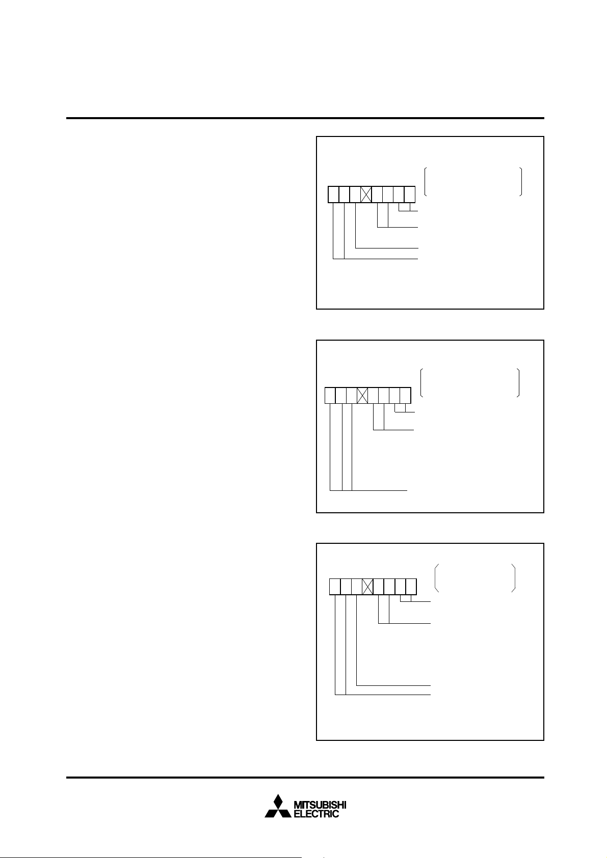
MITSUBISHI MICROCOMPUTERS
M37702M2AXXXFP, M37702M2BXXXFP
M37702S1AFP, M37702S1BFP
SINGLE-CHIP 16-BIT CMOS MICROCOMPUTER
(2) Event counter mode [01]
Figure 29 shows the bit configuration of the timer Bi mode register
during event counter mode. In event counter mode, the bit 0 in the
timer Bi mode register must be “1” and bit 1 must be “0”.
The input signal from the TBi
IN pin is counted when the count start
flag is “1” and counting is stopped when it is “0”. Count is performed at the fall of the input signal when bits 2, and 3 are “0” and
at the rise of the input signal when bit 3 is “0” and bit 2 is “1”.
When bit 3 is “1” and bit 2 is “0”, count is performed at the rise and
fall of the input signal.
Data write, data read and timer interrupt are performed in the
same way as for timer mode.
(3) Pulse period measurement/pulse width
measurement mode [10]
Figure 30 shows the bit configuration of the timer Bi mode register
during pulse period measurement/pulse width measurement
mode.
In pulse period measurement/pulse width measurement mode, bit
0 must be “0” and bit 1 must be “1”. Bits 6 and 7 are used to select
the clock source. The selected clock is counted when the count
start flag is “1” and counting stops when it is “0”.
The pulse period measurement mode is selected when bit 3 is “0”.
In pulse period measurement mode, the selected clock is counted
during the interval starting at the fall of the input signal from the
TBi
IN pin to the next fall or at the rise of the input signal to the next
rise and the result is stored in the reload register. In this case, the
reload register acts as a buffer register.
When bit 2 is “0”, the clock is counted from the fall of the input signal to the next fall. When bit 2 is “1”, the clock is counted from the
rise of the input signal to the next rise.
In the case of counting from the fall of the input signal to the next
fall, counting is performed as follows. As shown in Figure 31,
when the fall of the input signal from TBi
tents of the counter is transferred to the reload register. Next the
counter is cleared and count is started from the next clock. When
the fall of the next input signal is detected, the contents of the
counter is transferred to the reload register once more, the
counter is cleared, and the count is started. The period from the
fall of the input signal to the next fall is measured in this way.
IN pin is detected, the con-
76543210
✕✕ ✕
Timer B0 mode register 5B
Timer B1 mode register 5C
Timer B2 mode register 5D
0
0
0 0 : Always “00” in timer mode
✕ ✕ : Not used in timer mode and
may be any
✕ : Not used in timer mode
Clock source selection bit
0 0 : Select f
0 1 : Select f16
1 0 : Select f
1 1 : Select f
Fig. 28 Timer Bi mode register bit configuration during timer
mode
76543210
1
✕✕✕
Timer B0 mode register 5B
Timer B1 mode register 5C
Timer B2 mode register 5D
0
0 1 : Always “01” in event counter
mode
0 0 : Count at the falling edge of input
signal
0 1 : Count at the rising edge of input
signal
1 0 : Count at the both falling edge and
rising edge of input signal
✕ ✕ ✕ : Not used in event counter mode
Fig. 29 Timer Bi mode register bit configuration during event
counter mode
76543210
Timer B0 mode register 5B
Timer B1 mode register 5C
01
Timer B2 mode register 5D
1 0 : Always “10” in pulse period
measurement/pulse width
measurement mode
0 0 : Count from the falling edge of
input signal to the next falling one
0 1 : Count from the rising edge of
input signal to the next rising one
1 0 : Count from the falling edge of input
signal to the next rising one
and from the rising edge to the
next falling one
Timer Bi overflow flag
Clock source selection bit
0 0 : Select f
0 1 : Select f
1 0 : Select f
1 1 : Select f
2
64
512
2
16
64
512
Addresses
16
16
16
Addresses
16
16
16
Addresses
16
16
16
Fig. 30 Timer Bi mode register bit configuration during pulse
period measurement/pulse width measurement mode
25
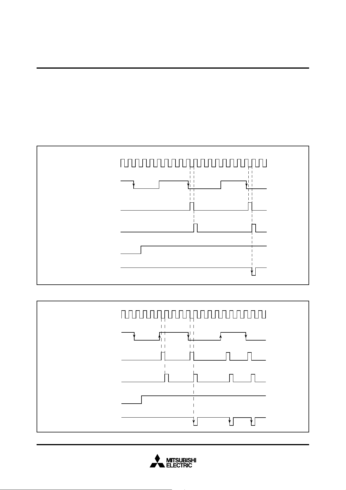
MITSUBISHI MICROCOMPUTERS
M37702M2AXXXFP, M37702M2BXXXFP
M37702S1AFP, M37702S1BFP
SINGLE-CHIP 16-BIT CMOS MICROCOMPUTER
After the contents of the counter is transferred to the reload register, an interrupt request signal is generated and the interrupt
request bit in the timer Bi interrupt control register is set. However,
no interrupt request signal is generated when the contents of the
counter is transferred first time to the reload register after the
count start flag is set to “1”.
When bit 3 is “1”, the pulse width measurement mode is selected.
Pulse width measurement mode is similar to pulse period measurement mode except that the clock is counted from the fall of the
TBi
IN pin input signal to the next rise or from the rise of the input
Selected clock
source f
Reload register←Counter
Count start flag
TBi
Counter←0
i
IN
signal to the next fall as shown in Figure 32.
When timer Bi is read, the contents of the reload register is read.
Note that in this mode, the interval between the fall of the TBi
IN pin
input signal to the next rise or from the rise to the next fall must be
at least two cycles of the timer count source.
Timer Bi overflow flag which is bit 5 of time Bi mode register is set
to “1” when the timer Bi counter reaches 0000
16.
This flag is cleared by writing to corresponding timer Bi mode register. This bit is set to “1” at reset.
Interrupt request signal
Fig. 31
Pulse period measurement mode operation (example of measuring the interval between the falling edge to next falling one)
Selected
clock source fi
IN
TBi
Reload register←Counter
Counter←0
Count start
flag
Interrupt
request signal
Fig. 32 Pulse width measurement mode operation
26
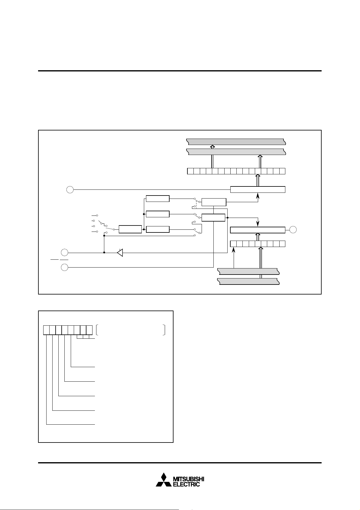
MITSUBISHI MICROCOMPUTERS
M37702M2AXXXFP, M37702M2BXXXFP
M37702S1AFP, M37702S1BFP
SINGLE-CHIP 16-BIT CMOS MICROCOMPUTER
SERIAL I/O PORTS
Two independent serial I/O ports are provided. Figure 33 shows a
block diagram of the serial I/O ports.
Bits 0, 1, and 2 of the UARTi (i = 0, 1) Transmit/Receive mode register shown in Figure 34 are used to determine whether to use port
P8 as parallel port, clock synchronous serial I/O port, or asynchro-
RxDi
1/16 Divider
Clock synchronous
1/16 Divider
Clock synchronous
1/2 Divider
Clock synchronous
(Internal clock)
CLKi
CTSi/RTSi
Clock source selection
f
2
f
16
f
64
f
512
External
Bit rate
generator
UART0(31
UART1(39
Internal
Clock synchronous
16
)
16
)
1/(n + 1)
Divider
(Internal clock)
nous (UART) serial I/O port using start and stop bits.
Figures 35 and 36 show the connections of receiver/transmitter
according to the mode.
Figure 37 shows the bit configuration of the UARTi transmit/receive control register.
Each communication method is described below.
Data bus (odd)
Data bus (even)
0000000 D7D6D5D4D3D2D1D
UART receive
UART transmission
Clock synchronous
(External clock)
Receive control
circuit
Transmission
control circuit
D
8
UART0 (37
UART1 (3F
Receive register
Receive clock
Transmission clock
Transmission register
D7D6D5D4D3D2D1D
D
8
Data bus (odd)
Data bus (even)
UART0 (33
UART1 (3B
0
16
, 3616)
16
, 3E16)
0
16
Receive
buffer register
TxDi
Transmission
buffer register
, 3216)
16
, 3A16)
Fig. 33 Serial I/O port block diagram
76543210
UART 0 transmit/receive mode register 30
UART 1 transmit/receive mode register 38
Serial communication method selection bits
0 0 0 : Parallel port
0 0 1 : Clock synchronous
1 0 0 : 7-bit UART
1 0 1 : 8-bit UART
1 1 0 : 9-bit UART
Internal clock/External clock selection bit
0 : Internal clock
1 : External clock
Stop bit length selection bit
0 : 1 stop bit
1 : 2 stop bits
Even/Odd parity selection bit
0 : Odd parity
1 : Even parity
Parity enable selection bit
0 : No parity
1 : With parity
Sleep selection bit
0 : No sleep
1 : Sleep
Fig. 34 UART i Transmit/ Receive mode register bit
configuration
Addresses
16
16
27

MITSUBISHI MICROCOMPUTERS
M37702M2AXXXFP, M37702M2BXXXFP
M37702S1AFP, M37702S1BFP
SINGLE-CHIP 16-BIT CMOS MICROCOMPUTER
Data bus (odd)
Data bus (even)
0 D
000000
RxDi
Stop
bit
2 stop bit
1 stop bit
Fig. 35 Receiver block diagram
2 stop bit
Stop
“0”
Stop
bit
bit
1 stop bit
Fig. 36 Transmitter block diagram
Stop
bit
Parity
Parity
bit
Synchronous
Parity
Parity
bit
7 bit
8 bit
9 bit
No
parity
“0”
7 bit
8 bit
9 bit
No
parity
Synchronous
8
9 bit
7 bit
8 bit
Synchronous
Data bus (odd)
Data bus (even)
D
8
7 bit
9 bit
Synchro-
nous
8 bit 7 bit
D
7
D6D5D4D3D2D
8 bit
9 bit
Synchronous
7 bit
D
7
D6D5D4D3D2D
8 bit
9 bit
Synchronous
1
1
Transmission register
D
0
D
0
Receive buffer
register
Receive
register
Transmission
buffer register
TxDi
76543210
Tx
R/C
1 CS0
EPTY
CS
76543210
SUM PER FER OER RI
RE TI
Fig. 37 UARTi Transmit/Receive control register bit configuration
UART 0 transmit/receive control register 0 3416
UART 1 transmit/receive control register 0 3C16
Clock source selection bits
0 0 : Select f
0 1 : Select f16
1 0 : Select f64
1 1 : Select f512
CTS, RTS Selection bit
0 : Select
1 : Select RTS
2
CTS
Transmission register empty bit
UART 0 transmit/receive control register 1 35
TE
UART 1 transmit/receive control register 1 3D16
Transmit enable flag
Transmit buffer empty flag
Receive enable flag
Receive completion flag
Overrun error flag
Framing error flag
Parity error flag
Error sum flag
Addresses
Addresses
16
28

MITSUBISHI MICROCOMPUTERS
M37702M2AXXXFP, M37702M2BXXXFP
M37702S1AFP, M37702S1BFP
SINGLE-CHIP 16-BIT CMOS MICROCOMPUTER
CLOCK SYNCHRONOUS SERIAL COMMUNICATION
A case where communication is performed between two clock synchronous serial I/O ports as shown in Figure 38 will be described.
(The transmission side will be denoted by subscript j and the receiving side will be denoted by subscript k.)
Bit 0 of the UARTj transmit/receive mode register and UARTk
transmit/receive mode register must be set to “1” and bits 1 and 2
must be “0”. The length of the transmission data is fixed at 8 bits.
Bit 3 of the UARTj transmit/receive mode register of the clock
sending side is cleared to “0” to select the internal clock. Bit 3 of
the UARTk transmit/receive mode register of the clock receiving
side is set to “1” to select the external clock. Bits 4, 5 and 6 are ignored in-clock synchronous mode. Bit 7 must always be “0”.
The clock source is selected by bit 0 (CS
0) and bit 1 (CS1) of the
clock sending side UARTj transmit/receive control register 0. As
shown in Figure 33, the selected clock is divided by (n +1), then
by 2, passed through a transmission control circuit, and output as
transmission clock CLKj. Therefore, when the selected clock is fi,
Bit Rate = fi
On the clock receiving side, the CS
{(n + 1) ✕ 2}
/
0 and CS1 bits of the UARTk
transmit/receive control register 0 are ignored because an external
clock is selected.
The bit 2 of the clock sending side UARTj transmit/receive control
register 0 is clear to “0” to select CTSj input. The bit 2 of the clock
receiving side is set to “1” to select RTSk output. CTS, and RTS
____
_____
____ ____
signals are described later.
Transmission
Transmission is started when the bit 0 (TEj flag) of UARTj transmit/receive control register 1 is “1”, bit 1 (Tlj flag) of one is “0”, and
____
CTSj input is “L”. As shown in Figure 39, data is output from TxDj
pin when transmission clock CLKj changes from “H” to “L”. The
data is output from the least significant bit.
The Tlj flag indicates whether the transmission buffer register is
empty or not. It is cleared to “0” when data is written in the transmission buffer register and set to “1” when the contents of the
transmission buffer register is transferred to the transmission register.
When the transmission register becomes empty after the contents
has been transmitted, data is transferred automatically from the
transmission buffer register to the transmission register if the next
transmission start condition is satisfied. If the bit 2 of UARTj transmit/receive control register 0 is “1”, CTSj input is ignored and
transmission start is controlled only by the TEj flag and TIj flag.
Once transmission has started, the TEj flag, TIj flag, and CTSj signals are ignored until data transmission completes. Therefore,
transmission is not interrupt when CTSj input is changed to “H”
during transmission.
The transmission start condition indicated by TEj flag, TIj flag, and
____
CTSj is checked while the TENDj signal shown in Figure 39 is “H”.
Therefore, data can be transmitted continuously if the next transmission data is written in the transmission buffer register and TIj
flag is cleared to “0” before the T
____
____
____
ENDj signal goes “H”.
The bit 3 (TxEPTYj flag) of UARTj transmit/receive control register 0 changes to “1” at the next cycle after the T
ENDj signal goes
“H” and changes to “0” when transmission starts. Therefore, this
flag can be used to determine whether data transmission has
completed.
When the TIj flag changes from “0” to “1”, the interrupt request bit
in the UARTj transmission interrupt control register is set to “1”.
Receive
Receive starts when the bit 2 (REk flag) of UARTk transmit/receive
control register 1 is set to “1”.
_____
The RTSk output is “H” when the REk flag is “0” and goes “L” when
the RE
k flag changed to “1”. It goes back to “H” when receive
starts. Therefore, the RTSk output can be used to determine
whether the receive register is ready to receive. It is ready when
_____
RTSk output is “L”.
The data from the RxD
ceive register is shifted by 1 bit each time the transmission clock
CLKj changes from “L” to “H”. When an 8-bit data is received, the
contents of the receive register is transferred to the receive buffer
register and the bit 3 (RI
register 1 is set to “1”. In other words, the setting of the RI
dicates that the receive buffer register contains the received data.
At this point, RTSj output goes “L” to indicate that the next data
_____
can be received. When the RI
terrupt request bit in the UART
set to “1”. Bit 4 (OER
ister is set to “1” when the next data is transferred from the receive
register to the receive buffer register while RI
cates that the next data was transferred to the receive register
before the contents of the receive buffer register was read.
RI
k and OERk flags are cleared automatically to “0” when the low-
order byte of the receive buffer register is read. The OER
also cleared when the RE
(PER
k flag), and bit 7 (SUMk flag) are ignored in clock synchro-
nous mode.
As shown in Figure 33, with clock synchronous serial communication, data cannot be received unless the transmitter is operating
because the receive clock is created from the transmission clock.
Therefore, the transmitter must be operating even when there is
no data to be sent from UART
_____
k pin is retrieved and the contents of the re-
k flag) of UARTk transmit/receive control
k flag in-
k flag changes from “0” to “1”, the in-
k receive interrupt control register is
k flag) of UARTk transmit/receive control reg-
k flag is “1”, and indi-
k flag is
k flag is cleared. Bit 5 (FERk flag), bit 6
k to UARTj.
29
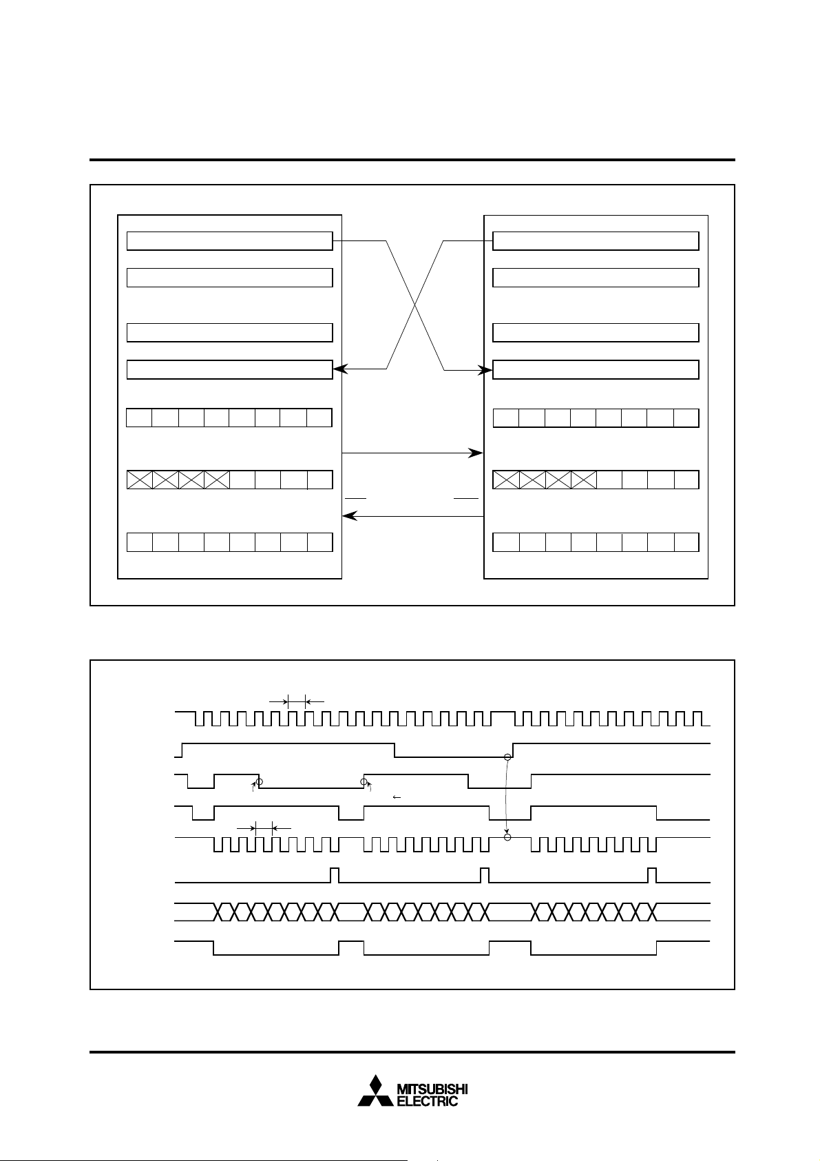
MITSUBISHI MICROCOMPUTERS
M37702M2AXXXFP, M37702M2BXXXFP
M37702S1AFP, M37702S1BFP
SINGLE-CHIP 16-BIT CMOS MICROCOMPUTER
UARTj transmission register
UART
j
transmission buffer register
UART
j
receive buffer register
UART
j
receive register
j
transmit/receive mode register
UART
✕0 ✕✕000
1
UARTj transmit/receive control register 0
Tx
Tx
EPTY
EPTY
UART
j
transmit/receive control register 1
0
0
CS
1CS0
CS1CS
0
RIPERSUM FER OER RE TI TE
Fig. 38 Clock synchronous serial communication
TxD
RxD
CLK
CTS
j
j
j
j
TxD
RxD
CLK
RTS
k
k
k
k
UARTk transmission register
UART
k
transmission buffer register
UART
k
receive buffer register
k
receive register
UART
k
transmit/receive mode register
UART
000
✕✕✕
k
transmit/receive control register 0
UART
UART
k
transmit/receive control register 1
1
Tx
1 ✕✕
EPTY
1
FER RIPERSUM OER RE TI TE
Transmission
clock
TE
j
TI
j
Write in transmission buffer register
CTSj
1 / fi ✕ ( n + 1 ) ✕ 2
j
CLK
T
ENDj
TXD
TXEPTY
j
j
D0D1D2D3D
4
Fig. 39 Clock synchronous serial I/O timing
30
1 / fi ✕ ( n + 1 ) ✕ 2
Transmission register Transmission buffer register
D
5
D6D
D0D1D2D3D
7
4
D5D6D
Stopped because TEj = “0”
7
D0D1D2D3D4D5D6D
7

MITSUBISHI MICROCOMPUTERS
M37702M2AXXXFP, M37702M2BXXXFP
M37702S1AFP, M37702S1BFP
SINGLE-CHIP 16-BIT CMOS MICROCOMPUTER
ASYNCHRONOUS SERIAL
COMMUNICATION
Asynchronous serial communication can be performed using 7-,
8-, or 9-bit length data. The operation is the same for all data
lengths. The following is the description for 8-bit asynchronous
communication.
With 8-bit asynchronous communication, the bit 0 of UARTi transmit/receive mode register is “1“, the bit 1 is “0”, and the bit 2 is “1”.
Bit 3 is used to select an internal clock or an external clock. If bit 3
is “0”, an internal clock is selected and if bit 3 is “1”, then external
clock is selected. If an internal clock is selected, the bit 0 (CS
and bit 1 (CS
used to select the clock source. When an internal clock is selected
for asynchronous serial communication, the CLKi pin can be used
as a normal I/O pin.
Transmission clock
1) of UARTi transmit/receive control register 0 are
(1 / f1 , or 1 / f
TE
i
TI
i
CTS
i
Write in transmission buffer register
EXT
) ✕ (n + 1) ✕ 16
Transmission register ←
The selected internal or external clock is divided by (n +1), then by
16, and passed through a control circuit to create the UART transmission clock or UART receive clock.
Therefore, the transmission speed can be changed by changing
the contents n of the bit rate generator. If the selected clock is an
internal clock fi or an external clock f
Bit Rate = (f
i or fEXT)
/
{(n + 1) ✕ 16}
EXT,
Bit 4 is the stop bit length selection bit to select 1 stop bit or 2 stop
bits.
The bit 5 is a selection bit of odd parity or even parity.
0)
In the odd parity mode, the parity bit is adjusted so that the sum of
the 1’s in the data and parity bit is always odd.
In the even parity mode, the parity bit is adjusted so that the sum
of the 1’s in the data and parity bit is always even.
Transmission
buffer register
T
ENDi
Stopped because TEi = “0”
SP
P
ST
TXD
i
TXEPTY
Start bit
ST
D
D
1
0
i
D2D
D4D
3
Parity bit Stop bit
5
D6D
7
PSPST
D
D
0
1
D2D3D
D
5
4
D6D
7
Fig. 40 Transmit timing example when 8-bit asynchronous communication with parity and 1 stop bit is selected
(1 / f1 or 1 / f
EXT
) ✕ (n + 1) ✕ 16
Transmission clock
TE
i
TI
i
T
ENDi
TXD
i
TXEPTY
Write in transmission buffer register
Start bit
ST
i
1D2D3D4D5
D
0
D
Stop Bit Stop Bit
D
6
D
7
D
Transmission register ← Transmission
D
D1D2D3D4D
8
SP
SP
ST
0
buffer register
5
D6D
Stopped because
SP
ST
D
7
8
SP
Fig. 41 Transmit timing example when 9-bit asynchronous communication with no parity and 2 stop bits is selected
D
0
TEi = “0”
D
0D1
D
1
D
2
31

MITSUBISHI MICROCOMPUTERS
M37702M2AXXXFP, M37702M2BXXXFP
M37702S1AFP, M37702S1BFP
SINGLE-CHIP 16-BIT CMOS MICROCOMPUTER
Bit 6 is the parity bit selection bit which indicates whether to add
parity bit or not.
Bits 4 to 6 should be set or reset according to the data format of
the communicating devices.
Bit 7 is the sleep selection bit. The sleep mode is described later.
The UART
termine whether to use CTSi input or RTSi output.
____ ____
CTSi input is used if bit 2 is “0” and RTSi output is used if bit 2 is
“1”.
If CTSi input is selected, the user can control whether to stop or
start transmission by external CTSi input. RTSi will be described
i transmit/receive control register 0 bit 2 is used to de-
____
____ ____
____ ____
later.
Transmission
Transmission is started when the bit 0 (TEi flag) of UARTi transmit/
receive control register 1 is “1”, the bit 1 (TIi flag) is “0”, and CTSi
input is “L” if CTSi input is selected. As shown in Figure 40 and 41,
data is output from the TxD
specified by the bits 4 to 6 of UART
____
i pin with the stop bit and parity bit
i transmit/receive mode regis-
ter. The data is output from the least significant bit.
The TIi flag indicates whether the transmission buffer is empty or
not. It is cleared to “0” when data is written in the transmission
buffer and set to “1” when the contents of the transmission buffer
register is transferred to the transmission register.
____
When the transmission register becomes empty after the contents
has been transmitted, data is transferred automatically form the
transmission buffer register to the transmission register if the next
transmission start condition is satisfied.
Once transmission has started, the TEi flag, TIi flag, and CTSi sig-
____
nal (if CTSi input is selected) are ignored until data transmission is
____
completed.
Therefore, transmission does not stop until it completes even if the
TE
i flag is cleared during transmission.
The transmission start condition indicated by TE
____
CTSi is checked while the TENDi signal shown in Figure 40 is “H”.
i flag, TIi flag, and
Therefore, data can be transmitted continuously if the next transmission data is written in the transmission buffer register and TI
flag is cleared to 0 before the TENDi signal goes “H”.
The bit 3 (TxEPTY
0 changes to “1” at the next cycle after the T
i flag) of UARTi transmit/receive control register
ENDi signal goes “H”
and changes to “0” when transmission starts. Therefore, this flag
can be used to determine whether data transmission is completed.
When the TI
in the UART
i flag changes from “0” to “1”, the interrupt request bit
i transmission interrupt control register is set to “1”.
Receive
Receive is enabled when the bit 2 (REi flag) of UARTi transmit/receive control register 1 is set. As shown in Figure 42, the
frequency divider circuit at the receiving end begin to work when a
start bit is arrived and the data is received.
i
fi or f
EXT
RE
i
RxD
i
Start bit
Check to be “L” level Get data
D
0
1
D
7
D
Stop bit
Receive
Clock
RI
i
RTS
i
Starting at the falling
edge of start bit
Fig. 42 Receive timing example when 8-bit asynchronous communication with no parity and 1 stop bit is selected.
Start bit
32

MITSUBISHI MICROCOMPUTERS
M37702M2AXXXFP, M37702M2BXXXFP
M37702S1AFP, M37702S1BFP
SINGLE-CHIP 16-BIT CMOS MICROCOMPUTER
____
If RTSi output is selected by setting the bit 2 of UARTi transmit/receive control register 0 to “1”, the RTSi output is “H” when the REi
flag is “0”. When the REi flag changes to “1”, the RTSi output goes
“L” to indicate receive ready and returns to “H” once receive has
started. In other words, RTSi output can be used to determine ex-
____
____
____
ternally whether the receive register is ready to receive.
The entire transmission data bits are received when the start bit
passes the final bit of the receive block shown in Figure 35. At this
point, the contents of the receive register is transferred to the receive buffer register and the bit 3 of UART
register 1 is set. In other words, the RI
ceive buffer register contains data when it is set. If RTSi output is
selected, RTSi output goes “L” to indicate that the register is ready
____
i transmit/receive control
i flag indicates that the re-
____
to receive the next data.
The interrupt request bit in the UART
ister is set when the RI
The bit 4 (OER
i flag changes from “0” to “1”.
i flag) of UARTi transmission control register 1 is
i receive interrupt control reg-
set when the next data is transferred from the receive register to
the receive buffer register while the RI
when an overrun error occurs. If the OER
i flag is “1”. In other words
i flag is “1”, it indicates
that the next data has been transferred to the receive buffer register before the contents of the receive buffer register has been
read.
Bit 5 (FER
i flag) is set when the number of stop bits is less than
required (framing error).
Bit 6 (PER
Bit 7 (SUM
PER
i flag) is set when a parity error occurs.
i flag) is set when either the OERi flag, FERi flag, or the
i flag is set. Therefore, the SUMi flag can be used to deter-
mine whether there is an error.
The setting of the RIi flag, OER
i flag, FERi flag, and the PERi flag
is performed while transferring the contents of the receive register
to the receive buffer register. The RI
i OERi, FERi, PERi, and SUMi
flags are cleared when the low order byte of the receive buffer register is read or when the RE
i flag is cleared.
puters receive the same data. Each subordinate microcomputer
checks the received data, clears the sleep bit if bits 0 to 6 are its
own address and sets the sleep bit if not. Next the main microcomputer sends data with bit 7 cleared. Then the microcomputer
with the sleep bit cleared will receive the data, but the microcomputer with the sleep bit set will not. In this way, the main
microcomputer is able to communicate with only the designated
microcomputer.
Sleep mode
The sleep mode is used to communicate only between certain microcomputers when multiple microcomputers are connected
through serial I/O.
The sleep mode is entered when the bit 7 of UART
ceive mode register is set.
The operation of the sleep mode for an 8-bit asynchronous communication is described below.
When sleep mode is selected, the contents of the receive register
is not transferred to the receive buffer register if bit 7 (bit 6 if 7-bit
asynchronous communication and bit 8 if 9-bit asychronous communication) of the received data is “0”. Also the RI
PER
i, and the SUMi flag are unchanged. Therefore, the interrupt
request bit of the UART
i receive interrupt control register is also
unchanged.
Normal receive operation takes place when bit 7 of the received
data is “1”.
The following is an example of how the sleep mode can be used.
The main microcomputer first sends data with bit 7 set to “1” and
bits 0 to 6 set to the address of the subordinate microcomputer
which wants to communicate with. Then all subordinate microcom-
i transmit/re-
i, OERi, FERi,
33
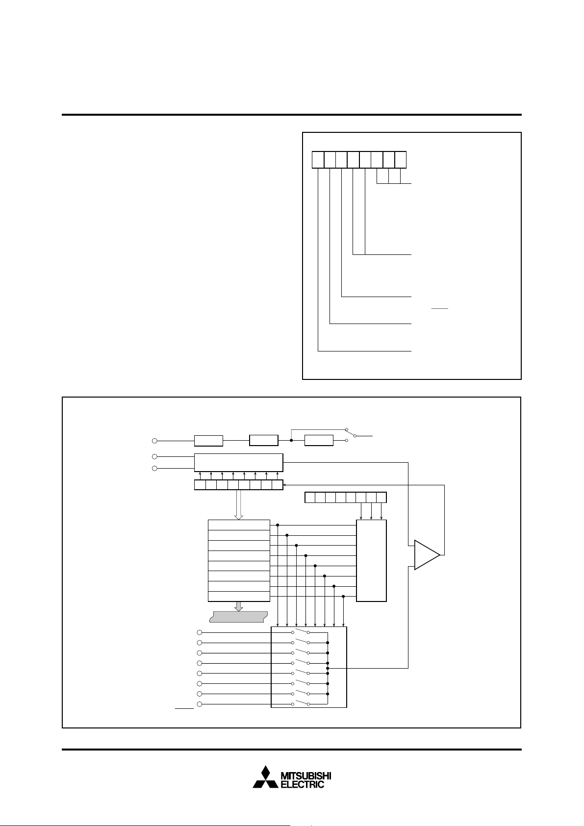
MITSUBISHI MICROCOMPUTERS
M37702M2AXXXFP, M37702M2BXXXFP
M37702S1AFP, M37702S1BFP
SINGLE-CHIP 16-BIT CMOS MICROCOMPUTER
A-D CONVERTER
The A-D converter is an 8-bit successive approximation converter.
Figure 43 shows a block diagram of the A-D converter and Figure
44 shows the bit configuration of the A-D control register. The frequency of the A-D converter operating clock φ
bit 7 of the A-D control register. When bit 7 is “0”, φ
frequency divided by 8. That is, φ
φ
AD is the clock frequency divided by 4 and φAD is = f(XIN)/4. The
φ
AD during A-D conversion must be 250 kHz minimum because
AD = f(XIN)/8. When bit 7 is “1”,
the comparator consists of a capacity coupling amplifier.
The operating mode is selected by the bits 3 and 4 of A-D control
register. The available operating modes are one-shot, repeat,
single sweep, and repeat sweep.
The bit of data direction register bit corresponding to the A-D converter pin must be “0” (input mode) because the analog input port
is shared with port P7.
The operation of each mode is described below.
AD is selected by the
AD is the clock
765432 01
A-D control register 1
Analog input selection bits
0 0 0 : Select AN
0 0 1 : Select AN
0 1 0 : Select AN
0 1 1 : Select AN
1 0 0 : Select AN
1 0 1 : Select AN
1 1 0 : Select AN
1 1 1 : Select AN
A-D operation mode selection bits
0 0 : One-shot mode
0 1 : Repeat mode
1 0 : Single sweep mode
1 1 : Repeat sweep mode
Trigger selection bit
0 : Software trigger
AD
TRG
1 :
A-D conversion start flag
0 : Stop A-D conversion
1 : Start A-D conversion
Frequency selection flag
0 : Select f(X
1 : Select f(X
input trigger
Fig 44 A-D control register bit configuration
0
1
2
3
4
5
6
7
IN
IN
)/8
)/4
Address
1E
16
f(XIN)
REF
V
AV
SS
1/2
Ladder network
Successive approximation register
A-D register 0 (20
A-D register 1 (22
A-D register 2 (24
A-D register 3 (26
A-D register 4 (28
A-D register 5 (2A
A-D register 6 (2C
A-D register 7 (2E
Data bus (even)
AN
0
AN
1
AN
2
AN
3
AN
4
AN
5
AN
6
AN
7
AD
TRG
2
f
1/2
Addresses
16
)
16
)
16
)
16
)
16
)
16
)
16
)
16
)
A-D conversion speed selection
1/2
Vref
A-D control register
(1E
16
)
Decoder
Selector
AD
φ
Comparator
Fig 43 A-D converter block diagram
34
MITSUBISHI MICROCOMPUTERS
M37702M2AXXXFP, M37702M2BXXXFP
M37702S1AFP, M37702S1BFP
SINGLE-CHIP 16-BIT CMOS MICROCOMPUTER
(1) One-shot mode [00]
The A-D conversion pins are selected with the bit 0 to 2 of A-D
control register. A-D conversion can be started by a software trigger or by an external trigger.
A software trigger is selected when the bit 5 of A-D control register
is “0” and an external trigger is selected when it is “1”.
When a software trigger is selected, A-D conversion is started
when bit 6 (A-D conversion start flag) is set. A-D conversion ends
after 57 φ
AD cycles and an interrupt request bit is set in the A-D
conversion interrupt control register. At the same time, A-D control
register bit 6 (A-D conversion start flag) is cleared and A-D conversion stops. The result of A-D conversion is stored in the A-D
register corresponding to the selected pin.
If an external trigger is selected, A-D conversion starts when the
A-D conversion start flag is “1” and the ADTRG input changes from
“H” to “L”. In this case, the pins that can be used for A-D conversion are AN0 to AN6 because the ADTRG pin is shared with the
analog voltage input pin AN
7. The operation is the same as with
______
______
software trigger except that the A-D conversion start flag is not
cleared after A-D conversion and a retrigger can be available during A-D conversion.
(2) Repeat mode [01]
The operation of this mode is the same as the operation of oneshot mode except that when A-D conversion of the selected pin is
complete and the result is stored in the A-D register, conversion
does not stop, but is repeated. Also, no interrupt request is issued
in this mode. Furthermore, if software trigger is selected, the A-D
conversion start flag is not cleared. The contents of the A-D register can be read at any time.
The operation is the same as done by software trigger except that
the A-D conversion start flag is not cleared after A-D conversion
and a retrigger can be available during A-D conversion.
(4) Repeat sweep mode [11]
The difference with the single sweep mode is that A-D conversion
does not stop after converting from the AN
pins, but repeats again from the AN
0 pin. The repeat is performed
among the selected pins. Also, no interrupt request is generated.
Furthermore, if software trigger is selected, the A-D conversion
start flag is not cleared. The A-D register can be read at any time.
7
6 5 4 3 2 1 0
A-D sweep pin
selection register
Fig. 45 A-D sweep pin selection register configuration
0 pin to the selected
Address
1F
0 0 : AN0, AN1 (2 pins)
0 1 : AN
1 0 : AN
1 1 : AN
0
to AN3 (4 pins)
0
to AN5 (6 pins)
0
to AN7 (8 pins)
16
(3) Single sweep mode [10]
In the sweep mode, the number of analog input pins to be swept
can be selected. Analog input pins are selected by bits 1 and 0 of
the A-D sweep pin selection register (1F
ure 45. Two pins, four pins, six pins, or eight pins can be selected
as analog input pins, depending on the contents of these bits.
A-D conversion is performed only for selected input pins. After
A-D conversion is performed for input of AN
result is stored in A-D register 0, and in the same way, A-D conversion is performed for selected pins one after another. After A-D
conversion is performed for all selected pins, the sweep is
stopped.
A-D conversion can be started with a software trigger or with an
external trigger input. A software trigger is selected when bit 5 is
“0” and an external trigger is selected when it is “1”.
When a software trigger is selected, A-D conversion is started
when A-D control register bit 6 (A-D conversion start flag) is set.
When A-D conversion of all selected pins end, an interrupt request
bit is set in the A-D conversion interrupt control register. At the
same time, A-D control register bit 6 (A-D conversion start flag) is
cleared and A-D conversion stops.
When an external trigger is selected, A-D conversion starts when
the A-D conversion start flag is “1” and the ADTRG input changes
from “H” to “L”. In this case, the A-D conversion result of the trigger input itself is stored in the A-D register 7 because the ADTRG
pin is shared with AN7 pin.
16 address) shown in Fig-
0 pin, the conversion
______
______
35

MITSUBISHI MICROCOMPUTERS
M37702M2AXXXFP, M37702M2BXXXFP
M37702S1AFP, M37702S1BFP
SINGLE-CHIP 16-BIT CMOS MICROCOMPUTER
WATCHDOG TIMER
The watchdog timer is used to detect unexpected execution sequence caused by software run-away.
Figure 46 shows a block diagram of the watchdog timer. The
watchdog timer consists of a 12-bit binary counter.
The watchdog timer counts the clock frequency divided by 32 (f
or by 512 (f
512). Whether to count f32 or f512 is determined by the
watchdog timer frequency selection flag shown in Figure 47. f
is selected when the flag is “0” and f32 is selected when it is “1”.
The flag is cleared after reset. FFF
when “L” or 2VCC is applied to the RESET pin, STP instruction is
16 is set in the watchdog timer
______
executed, data is written to the watchdog timer, or the most significant bit of the watchdog timer become “0”.
After FFF
16 is set in the watchdog timer, the contents of watchdog
timer is decremented by one at every cycle of selected frequency
f
32 or f512, and after 2048 counts, the most significant bit of watch-
dog timer become “0”, and a watchdog timer interrupt request bit
is set, and FFF
16 is preset in the watchdog timer.
Normally, a program is written so that data is written in the watchdog timer before the most significant bit of the watchdog timer
become “0”. If this routine is not executed due to unexpected program execution, the most significant bit of the watchdog timer
become eventually “0” and an interrupt is generated.
The processor can be reset by setting the bit 3 (software reset bit)
of processor mode register described in Figure 10 in the interrupt
section and generating a reset pulse.
The watchdog timer stops its function when the RESET pin voltage is raised to double the V
CC voltage.
______
The watchdog timer can also be used to recover from when the
clock is stopped by the STP instruction. Refer to the section on
clock generation circuit for more details.
The watchdog timer hold the contents during a hold state and the
frequency is stopped to input.
32)
512
Watchdog timer
32
frequency selection (connection forced to f
during
STP instruction execution)
f
32
f
512
Watchdog timer
Hold
(6016)
Write to watchdog
timer
RESET
STP instruction
2Vcc
detection
circuit
SQ
R
Fig. 46 Watchdog timer block diagram
7
6 5 4 3 2 1 0
Watchdog timer
frequency selection
0 : Select f
1 : Select f
512
32
Fig. 47 Watchdog timer frequency selection flag
Set “FFF16”
Address
61
16
36

MITSUBISHI MICROCOMPUTERS
M37702M2AXXXFP, M37702M2BXXXFP
M37702S1AFP, M37702S1BFP
SINGLE-CHIP 16-BIT CMOS MICROCOMPUTER
RESET CIRCUIT
Reset occurs when the RESET pin is returned to “H” level after
______
holding it at “L” level when the power voltage is at 5 V ± 10%. Program execution starts at the address formed by setting the
address pins A
FFFF
16, and A7 – A0 to the contents of address FFFE16.
23 – A16 to 0016, A15 – A8 to the contents of address
Figure 48 shows the status of the internal registers when a reset
occurs.
Figure 49 shows an example of a reset circuit. The reset input
voltage must be held 0.9 V or lower when the power voltage
reaches 4.5 V.
Address
(1) Port P0 data direction register
(2) Port P1 data direction register
(3) Port P2 data direction register
(4) Port P3 data direction register
(5) Port P4 data direction register
(6) Port P5 data direction register
(7) Port P6 data direction register
(8) Port P7 data direction register
(9) Port P8 data direction register
(10) A-D control register
A-D sweep pin selection register
(11)
(12)
UART 0 transmit/receive mode
register
(13)
UART 1 transmit/receive mode
register
(14)
UART 0 transmit/receive
(15)
(16)
(17)
(18) Count start flag
(19) One- shot start flag
(20) Up-down flag
(21) Timer A0 mode register
(22) Timer A1 mode register
(23) Timer A2 mode register
(24) Timer A3 mode register
(25) Timer A4 mode register
(26) Timer B0 mode register
(27) Timer B1 mode register
(28) Timer B2 mode register
control register 0
UART 1 transmit/receive
control register 0
UART 0 transmit/receive
control register 1
UART 1 transmit/receive
control register 1
16)•••
(04
(0516)•••
(0816)•••
(0916)•••
(0C16)•••
(0D16)•••
(1016)•••
(1116)•••
(1416)•••
(1E16)•••
(1F16)•••
(3016)•••
(3816)•••
(3416)•••
(3C16)•••
(3516)•••
(3D16)•••
(4016)•••
(4216)•••
(4416)•••
(5616)•••
(5716)•••
(5816)•••
(5916)•••
(5A16)•••
(5B16)•••
(5C16)•••
(5D16)•••
0016
00
16
0016
0000
0016
0016
0016
0016
0016
0
0000 ???
11
0016
0016
00
10
0010
0000
000010
0000
00
10
16
000 00
0016
0016
0016
0016
0016
0016
001 00 00
001
00 00
001 00 00
M37702M2AXXXFP
RESET
V
CC
0V
6928
0V
Power on
4.5V
0.9V
Fig. 49 Example of a reset circuit (perform careful evaluation
at the system design level before using)
Address
(29) Processor mode register
(30) Watchdog timer
Watchdog timer frequency selection
flag
(32)
A-D conversion interrupt control register
(33)
UART 0 transmission interrupt control
(34)
(35)
(36)
(37)
(38)
(39)
(40)
(41)
(42)
(43)
(44)
(45)
(46)
(47)
(48) Processor status register PS
(49) Program bank register PG
(50) Program counter PC
(51) Program counter PCL
(52) Direct page register DPR
(53) Data bank register DT
Contents of other registers and RAM are not initialized and should be initialized by software.
register
UART 0 receive interrupt control register
UART 1 transmission interrupt control
register
UART 1 receive interrupt control register
Timer A0 interrupt control register
Timer A1 interrupt control register
Timer A2 interrupt control register
Timer A3 interrupt control register
Timer A4 interrupt control register
Timer B0 interrupt control register
Timer B1 interrupt control register
Timer B2 interrupt control register
INT
0
interrupt control register
INT
1
interrupt control register
INT
2
interrupt control register
H
(5E16)•••
(6016)•••
(6116)•••(31)
(7016)•••
(7116)•••
(7216)•••
(7316)•••
(7416)•••
(7516)•••
(7616)•••
(7716)•••
(7816)•••
(7916)•••
(7A16)•••
(7B16)•••
(7C16)•••
(7D16)•••
(7E16)•••
(7F16)•••
0016
FFF16
0000
0000
0000
0000
0000
0000
0000
0000
0000
0000
0000
0000
0000
000
0
0
0
000
0
0
0
0
0
000
0
?
?000
00
1??
0
0016
Content of FFFF16
Content of FFFE16
000016
0016
00
Fig. 48 Microcomputer internal status during reset
37

MITSUBISHI MICROCOMPUTERS
M37702M2AXXXFP, M37702M2BXXXFP
M37702S1AFP, M37702S1BFP
SINGLE-CHIP 16-BIT CMOS MICROCOMPUTER
INPUT/OUTPUT PINS
Ports P8 to P0 all have a data direction register and each bit can
be programmed for input or output. A pin becomes an output pin
when the corresponding data direction register is set and an input
pin when it is cleared.
When pin programmed for output, the data is written to the port
latch and it is output to the output pin. When a pin is programmed
for output, the contents of the port latch is read instead of the
value of the pin. Therefore, a previously output value can be read
correctly even when the output “L” voltage is raised due to reasons such as directly driving an LED.
A pin programmed for input is floating and the value input to the
pin can be read. When a pin is programmed for input, the data is
written only in the port latch and the pin stays floating.
If an input/output pin is not used as an output port, clear the bit of
the corresponding data direction register so that the pin become
input mode.
Figure 50 shows a block diagram of ports P8 to P0 in single-chip
mode and the E pin output.
In memory expansion mode, microprocessor mode, and evaluation chip mode, ports P4 to P0 are also used as address, data,
and control signal pins.
Refer to the section on processor modes for more details.
_
38
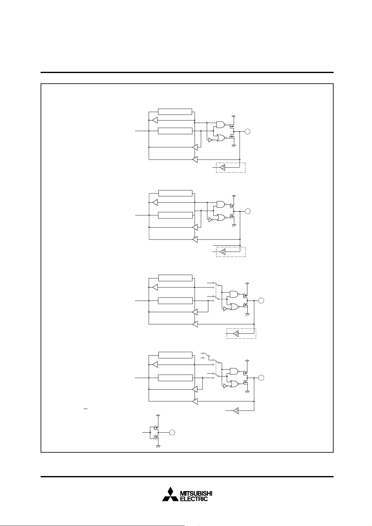
MITSUBISHI MICROCOMPUTERS
M37702M2AXXXFP, M37702M2BXXXFP
M37702S1AFP, M37702S1BFP
SINGLE-CHIP 16-BIT CMOS MICROCOMPUTER
• Ports P00 – P07, P10 – P17, P20 – P27, P30 – P33, P42 – P46 (Inside dotted-line not included)
0
, P41, P47, P57, P61 – P67, P82, P86 (Inside dotted-line included, but P82, P86 are without hysterisis)
Ports P4
Data direction register
Data bus
• Ports P70 – P76 (Inside dotted-line not included)
7
• Ports P7
(Inside dotted-line included)
Data direction register
Data bus
• Ports P83, P87 (Inside dotted-line not included)
• Ports P5
0
– P56, P60 (Inside dotted-line included)
Data direction register
Data bus
Port latch
Port latch
Port latch
Analog input
“1”
Output
• Ports P80, P81, P84, P8
5
Data bus
Data direction register
Port latch
“1”
“0”
Output
• E
Fig. 50_Block diagram for ports P8 to P0 in single-chip mode and the E pin output
39

MITSUBISHI MICROCOMPUTERS
M37702M2AXXXFP, M37702M2BXXXFP
M37702S1AFP, M37702S1BFP
SINGLE-CHIP 16-BIT CMOS MICROCOMPUTER
PROCESSOR MODE
The bits 0 and 1 of processor mode register as shown in Figure 51
are used to select any mode of single-chip mode, memory expansion mode, microprocessor mode, and evaluation chip mode.
Ports P3 to P0 and a part of port P4 are used as address, data,
and control signal I/O pins except in single-chip mode.
Figure 52 shows the functions of ports P4 to P0 in each mode.
The external memory area changes when the mode changes.
Figure 53 shows the memory map for each mode.
Refer to Figure 1 for the memory map of the single-chip mode.
The external memory area can be accessed except in single-chip
mode. The accessing of the external memory is affected by the
BYTE pin and the bit 2 (wait bit) of processor mode register.
These will be described next.
765432 01
0
• BYTE pin
When accessing the external memory, the level of the BYTE pin is
used to determine whether to use the data bus as 8-bit width or
16-bit width.
The data bus width is 8 bits when the level of the BYTE pin is “H”
and port P2 becomes the data I/O pin.
The data bus width is 16 bits when the level of the BYTE pin is “L”
and ports P1 and P2 become the data I/O pins.
When accessing the internal memory, The data bus width is always 16 bits regardless of the BYTE pin level.
An exclusive mode in the evaluation chip mode allows the BYTE
pin level to be set to 2·V
different from the above. This is described in the evaluation chip
mode section.
Processor mode register
Processor mode bit
0 0 : Single-chip mode
0 1 : Memory expansion mode
1 0 : Microprocessor mode
1 1 : Evaluation chip mode
Wait bit
0 : Wait
1 : No Wait
CC. In this case, the operation is slightly
Address
16
5E
Fig. 51 Processor mode register bit configuration
Software reset bit
Reset occurs when this bit is set to 1
Interrupt priority resolusion time selection bit
0 0 : Select 1/f (X
0 1 : Select 1/f (X
1 0 : Select 1/f (X
Test mode bit
This bit must be "0"
Clock φ1 output selection bit
0 : No φ
1 : φ
1 output
IN) ✕ 14
IN) ✕ 8
IN) ✕ 4
1 output
40
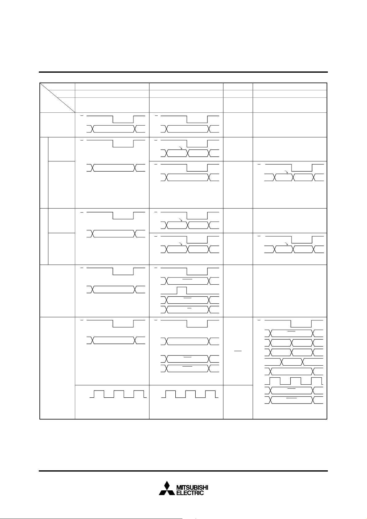
MITSUBISHI MICROCOMPUTERS
M37702M2AXXXFP, M37702M2BXXXFP
M37702S1AFP, M37702S1BFP
SINGLE-CHIP 16-BIT CMOS MICROCOMPUTER
CM
Port
CM
Mode
1
0
0
0
Single-chip Mode Memory Expansion Mode Evaluation Chip Mode
0
1
1
0
Microprocessor
Mode
1
1
Port P0
BYTE =“L”
BYTE =“H”
Port P1Port P2
or 2 • V
(Evaluation
chip mode
only.)
BYTE =“L”
BYTE =“H”
or 2 • V
(Evaluation
chip mode
only.)
Port P3
E
7
P0
P0
to
0
I/O Port
E
P1
7
to
P1
0
CC
I/O Port
E
P2
7
to
P2
0
CC
I/O Port
E
P3
3
P3
to
0
I/O Port
P1
P1
P1
P1
P2
P2
P2
P2
P3
P3
P3
P3
P0
P0
E
E
E
to
E
to
E
E
7
to
0
7
to
0
7
to
0
A23 to A
7
0
A23 to A
7
0
3
2
1
0
15 to A8
A
Address A
Address
Address A
16
Address
16
Address
ALE
7
Data(odd)
15
(even, odd)
HLDA
BHE
R
/W
to A
to A
Data
(even)
Data
0
8
Same as left Same as left
Same as left
Same as left
Same as left
Same as left
E
P1
to
P1
Ports P4, P5 and their direction
registers are treated as 16-bit wide
bus. If BYTE = 2 • V
ROM area is also treated as 16-bit
wide bus.
E
P2
to
P2
7
0
7
0
A15 to A
23
to A
A
Same as left
8
Address
Same as left
16
Address
Data(odd)
CC
(even, odd)
, the internal
Data
Same as for Port P1
Same as left
Same as left
Port P4
E
P4
7
to
P4
0
When processor mode
✽
register bit 7 =“0”
P4
2
I/O Port
φ
1
Same as above except P4
When processor mode
✽
register bit 7 =“1”
2
P4
P4
P4
P4
P4
E
to
✽
Fig. 52 Processor mode and ports P4 to P0 functions
7
2
1
0
2
I/O Port
RDY
HOLD
When processor mode
✽
register bit 7 =“0”
φ
1
Same as above except P4
When processor mode
register bit 7 =“1”
E
P4
7
P4
6
P4
5
P4
4
P4
3
P4
2
P4
Same as left in
2
spite of proces
-sor mode regi
-ster bit 7
P4
1
0
DBC
VPA
VDA
QCL
MX
1
φ
RDY
HOLD
41

MITSUBISHI MICROCOMPUTERS
M37702M2AXXXFP, M37702M2BXXXFP
M37702S1AFP, M37702S1BFP
SINGLE-CHIP 16-BIT CMOS MICROCOMPUTER
• Wait bit
As shown in Figure 54, when the external memory area is accessed with the processor mode register bit 2 (wait bit) cleared to
“0”, the “L” width of E signal becomes twice compared with no wait
(the wait bit is “1”). The wait bit is cleared to “0” at reset.
The accessing of internal memory area is performed in no wait
mode regardless of the wait bit.
The processor modes are described below.
Memory expansion
80
27F
C000
FFFF
FFFFFF
The shaded area is the external memory area.
Fig. 53 External memory area for each processor mode
_
Microprocessor
mode
2
16
9
16
16
RAM
16
16
mode
RAM
Evaluation
chip mode
2
16
9
16
A
16
C
16
RAM
ROM
16
16
(1) Single-chip mode [00]
Single-chip mode is entered by connecting the CNVSS pin to VSS
and starting from reset. Ports P4 to P0 all function as normal I/O
ports. Port P4
2 can be the φ1 output pin divided the clock to XIN
pin by 2 by setting bit 7 of processor mode register to “1”.
(2) Memory expansion mode [01]
Memory expansion mode is entered by setting the processor
mode bits to “01” after connecting the CNV
ing from reset.
Port P0 becomes an address output pin and loses its I/O port
function.
Port P1 has two functions depending on the level of the BYTE pin.
When the BYTE pin level is “L”, port P1 functions as an address
output pin while E is “H” and as an odd address data I/O pin while
_
E is “L”. However, if an internal memory is read, external data is
ignored while E is “L”. In this case the I/O port function is lost.
_
_
When the BYTE pin level “H”, port P1 functions as an address output pin and loses its I/O port function.
Port P2 has two functions depending on the level of the BYTE pin.
When the BYTE pin level is “L”, port P2 functions as an address
output pin while E is “H” and as an even address data I/O pin
_
while E is “L”. However, if an internal memory is read, external
data is ignored while E is “L”.
When the BYTE pin level is “H”, port P2 functions as an address
output pin while E is “H” and as an even and odd address data I/O
pin while E is “L”. However, if an internal memory is read, external
data is ignored while E is “L”. In this case the I/O port function is
_
_
_
_
_
lost.
Ports P30, P31, P32, and P33 become R/W, BHE, ALE, and HLDA
output pin respectively and lose their I/O port functions.
__
R/W is a read/write signal which indicates a read when it is “H”
and a write when it is “L”.
____
BHE is a byte high enable signal which indicates that an odd address is accessed when it is “L”.
Therefore, two bytes at even and odd addresses are accessed simultaneously if address A0 is “L” and BHE is “L”.
SS pin to VSS and start-
__
____ _____
____
Internal clock φ
Wait bit
“1”
Wait bit
“0”
Port P2
E
ALE
Port P2
E
ALE
Address
Address
Data
Data
Address
Data
Address
Data
Fig. 54 Relationship between wait bit and access time
42

MITSUBISHI MICROCOMPUTERS
M37702M2AXXXFP, M37702M2BXXXFP
M37702S1AFP, M37702S1BFP
SINGLE-CHIP 16-BIT CMOS MICROCOMPUTER
ALE is an address latch enable signal used to latch the address
signal from a multiplexed signal of address and data. The latch is
transparent while ALE is “H” to let the address signal pass through
and held while ALE is “L”.
_____
HLDA is a hold acknowledge signal and is used to notify externally
when the microcomputer receives HOLD input and enters into
hold state.
Ports P40 and P41 become HOLD and RDY input pin respectively
_____
_____ ____
and lose their output pin function, but the input pin function remains.
_____
HOLD is a hold request signal. It is an input signal used to put the
microcomputer in hold state. HOLD input is accepted when the in-
_____
ternal clock φ falls from “H” level to “L” level while the bus is not
used. Ports P0, P1, P2, P3
computer stays in hold state. These ports are floating after one
cycle of the internal clock φ later than HLDA signal changes to “L”
level. At the removing of hold state, these ports are removed from
floating state after one cycle of φ later than HLDA signal changes
to “H” level.
____
RDY is a ready signal. If this signal goes “L”, the internal clock φ
stops at “L”. When φ
bit 7 of processor mode register to “1”, φ1 output keeps on. RDY is
0, and P31 are floating while the micro-
_____
_____
1 output from port P42 is selected by setting
____
used when slow external memory is attached.
(3) Microprocessor mode [10]
Microprocessor mode is entered by connecting the CNVSS pin to
V
CC and starting from reset. It can also be entered by program-
ming the processor mode bits to “10” after connecting the CNV
SS
pin to VSS and starting from reset. This mode is similar to memory
expansion mode except that internal ROM is disabled and an external memory is required, and φ
1 from port P42 is always output
in spite of bit 7 of processor mode register.
(4) Evaluation chip mode [11]
Evaluation chip mode is entered by applying voltage twice the VCC
voltage to the CNVSS pin. This mode is normally used for evaluation tools.
The functions of ports P0 and P3 are the same as in memory expansion mode.
Port P1 functions as an address output pin while E is “H” and as
data I/O pin of odd addresses while E is “L” regardless of the
BYTE pin level. However, if an internal memory is read, external
data is ignored while E is “L”.
_
Port P2 function as an address output pin while E is “H” and as
data I/O pin of even addresses while E is “L” when the BYTE pin
level is “L”. However, if an internal memory is read, external data
is ignored while E is “L”.
When the BYTE pin level is “H” or 2·V
address output pin while E is “H” and as data I/O pin of even and
odd addresses while E is “L”. However, if an internal memory is
_
_
_
read, external data is ignored while E is “L”.
_
_
CC, port P2 functions as an
_
Port P4 and its data direction register which are located at address 0A
16 and 0C16 are treated differently in evaluation chip
mode. When these addresses are accessed, the data bus width is
treated as 16 bits regardless of the BYTE pin level, and the access cycle is treated as internal memory regardless of the wait bit.
_
_
When a voltage twice the V
CC voltage is applied to the BYTE pin,
the addresses corresponding to the internal ROM area are also
treated as 16-bit data bus.
The functions of ports P4
0 and P41 are the same as in memory
expansion mode.
Ports P4
2 to P46 become φ1, MX, QCL, VDA, and VPA output pins
respectively. Port P47 becomes the DBC input pin.
φ
1 from port P42 divided the clock to XIN pin by 2 is always output
____
in spite of bit 7 of processor mode register.
The MX signal normally contains the contents of flag m, but the
contents of flag x is output if the CPU is using flag x.
QCL is the queue buffer clear signal. It becomes “H” when the instruction queue buffer is cleared, for example, when a jump
instruction is executed.
VDA is the valid data address signal. It becomes “H” while the
CPU is reading data from data buffer or writing data to data buffer.
It also becomes “H” when the first byte of the instruction (operation code) is read from the instruction queue buffer.
VPA is the valid program address signal. It becomes “H” while the
CPU is reading an instruction code from the instruction queue
buffer.
____
DBC is the debug control signal and is used for debugging. Table
5 shows the relationship between the CNV
SS pin input levels and
processor modes.
Table 5. Relationship between the CNVSS pin input levels and
processor modes
CNVSS Mode
• Single-chip
VSS
• Memory expansion
• Microprocessor
• Evaluation chip
Description
Single-chip mode upon
starting after reset. Other
modes can be selected by
changing the processor
mode bit by software.
• Microprocessor
• Evaluation chip
VCC
Microprocessor mode upon
starting after reset. Evaluation chip mode can be
selected by changing the
processor mode bit by software.
2·VCC
• Evaluation chip
• Evaluation chip mode only.
43
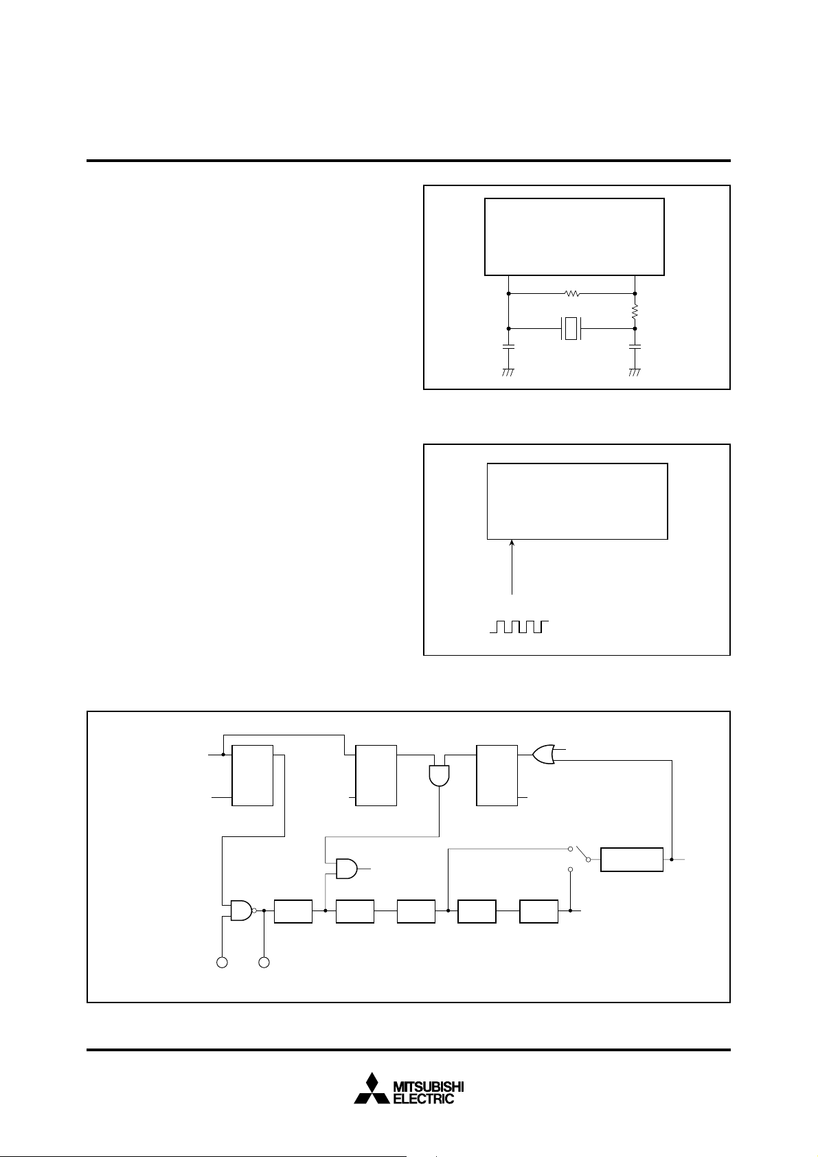
MITSUBISHI MICROCOMPUTERS
M37702M2AXXXFP, M37702M2BXXXFP
M37702S1AFP, M37702S1BFP
SINGLE-CHIP 16-BIT CMOS MICROCOMPUTER
CLOCK GENERATING CIRCUIT
Figure 55 shows a block diagram of the clock generator.
When an STP instruction is executed, the internal clock φ stops
oscillating at “L” level. At the same time, FFF
dog timer and the watchdog timer input connection is forced to f
16 is written to watch-
32.
This connection is broken and connected to the input determined
by the watchdog timer frequency selection flag when the most significant bit of the watchdog timer is cleared or reset.
Oscillation resumes when an interrupt is received, but the internal
clock φ remains at “L” level until the most significant bit of the
watchdog timer is cleared. This is to avoid the unstable interval at
the start of oscillation when using a ceramic resonator.
When a WIT instruction is executed, the internal clock φ stops at
“L” level, but the oscillator does not stop. The clock is restarted
when an interrupt is received. Instructions can be executed immediately because the oscillator is not stopped.
The stop or wait state is released when an interrupt is received or
when reset is issued. Therefore, interrupts must be enabled before executing a STP or WIT instruction.
Figure 56 shows a circuit example using a ceramic (or quartz crystal) resonator. Use the manufacture’s recommended values for
constants such as capacitance which differ for each resonator.
Figure 57 shows an example of using an external clock signal.
Fig. 56 Circuit using a ceramic resonator
M37702M2AXXXFP
X
IN
M37702M2AXXXFP
X
IN
29
1MΩ
X
OUT
X
OUT
Open
3029
Rd
30
Interrupt request
STP instruction
External clock source
Vcc
Vss
Fig. 57 External clock input circuit
QS
R
WIT instruction
QS
R
QS
R
Reset
STP instruction
Watchdog
Internal clock φ
f
2
f
16
f
32
f
64
1/2 1/8 1/2 1/2 1/8
X
X
OUT
IN
timer
f
512
Fig. 55 Block diagram of a clock generator
44

MITSUBISHI MICROCOMPUTERS
M37702M2AXXXFP, M37702M2BXXXFP
M37702S1AFP, M37702S1BFP
SINGLE-CHIP 16-BIT CMOS MICROCOMPUTER
ADDRESSING MODES
The M37702M2AXXXFP has 28 powerful addressing modes.
Refer to the 7700 Family addressing mode description for the details of each addressing mode.
MACHINE INSTRUCTION LIST
The M37702M2AXXXFP has 103 machine instructions. Refer to
the 7700 Family machine instruction list for details.
DATA REQUIRED FOR MASK ORDERING
Please send the following data for mask orders.
(1) Mask ROM order confirmation form
(2) 80P6N mark specification form
(3) ROM data (EPROM 3 sets)
45

MITSUBISHI MICROCOMPUTERS
M37702M2AXXXFP, M37702M2BXXXFP
M37702S1AFP, M37702S1BFP
SINGLE-CHIP 16-BIT CMOS MICROCOMPUTER
M37702M2AXXXFP
ELECTRICAL CHARACTERISTICS (VCC = 5 V, VSS = 0 V, Ta = 25 °C, f(XIN) = 16 MHz, unless otherwise noted)
Symbol Parameter Test conditions Unit
VOH
VOH
VOH
VOH
VOL
VOL
VOL
VOL
VT+ – VT–
VT+ – VT–
VT+ – VT–
IIH
IIL
VRAM
ICC
High-level output voltage P00–P07, P10–P17, P20–P27,
0
, P31, P33, P40–P47,
P3
P5
0
–P57, P60–P67, P70–P77,
0
–P8
7
P8
High-level output voltage P00–P07, P10–P17, P20–P27,
P3
0
, P31, P3
3
High-level output voltage P3
2
High-level output voltage_E
Low-level output voltage P0
0
–P07, P10–P17, P20–P27,
0
, P31, P33, P40–P47,
P3
P5
0
–P57, P60–P67, P70–P77,
0
–P8
7
P8
Low-level output voltage P00–P07, P10–P17, P20–P27,
P3
0
, P31, P3
3
Low-level output voltage P3
2
Low-level output voltage_E
_____
Hysteresis
Hysteresis
Hysteresis X
____
HOLD, RDY, TA0IN–TA4IN, TB0IN–TB2IN,
____ ____
INT0–INT2, AD
______
RESET
IN
_____
_____ _____
TRG
, CTS0, CTS1, CLK0, CLK
High-level input current P00–P07, P10–P17, P20–P27,
0
–P33, P40–P47, P50–P57,
P3
P6
0
–P67, P70–P77, P80–P8
______
XIN, RESET, CNVSS, BYTE
0
Low-level input current P0
–P07, P10–P17, P20–P27,
P3
0
–P33, P40–P47, P50–P57,
0
–P67, P70–P77, P80–P8
P6
______
XIN, RESET, CNVSS, BYTE
RAM hold voltage
Power supply current
IOH = –10 mA
OH = –400 µA
I
OH = –10 mA
I
OH = –400 µA
I
OH = –10 mA
I
OH = –400 µA
I
OL = 10 mA
I
OL = 2 mA
I
OL = 10 mA
I
OL = 2 mA
I
OL = 10 mA
I
OL = 2 mA
I
1
I = 5 V
V
7,
I = 0 V
V
7,
When clock is stopped.
In single-chip
mode output only
pin is open and
other pins are
SS during reset.
V
f(XIN) = 16 MHz,
square waveform
a = 25 °C when
T
clock is stopped.
a = 85 °C when
T
clock is stopped.
Limits
Min. Typ. Max.
3
4.7
3.1
4.8
3.4
4.8
0.45
1.9
0.43
1.6
0.4
0.4
0.2
0.1
0.5
0.3
–5
2
12
24
20
V
V
V
V
2
V
V
V
V
1
V
V
V
5
µA
µA
V
mA
1
µA
A-D CONVERTER CHARACTERISTICS (VCC = 5 V, VSS = 0 V, Ta = 25 °C, f(XIN) = 16 MHz, unless otherwise noted)
Symbol Parameter Test conditions Unit
LADDER
R
tCONV
VREF
VIA
—
—
Resolution
Absolute accuracy
Ladder resistance
Conversion time
Reference voltage
Analog input voltage
REF = VCC
V
VREF = VCC
VREF = VCC
Min. Typ. Max.
14.25
46
Limits
8
±3
2
2
0
10
CC
V
VREF
Bits
LSB
kΩ
µs
V
V

MITSUBISHI MICROCOMPUTERS
M37702M2AXXXFP, M37702M2BXXXFP
M37702S1AFP, M37702S1BFP
SINGLE-CHIP 16-BIT CMOS MICROCOMPUTER
ABSOLUTE MAXIMUM RATINGS
RatingsSymbol Parameter Conditions Unit
VCC
AVCC
VI
VI
VO
Pd
Topr
Tstg
Supply voltage
Analog supply voltage
Input voltage
Input voltage P0
______
RESET, CNVSS, BYTE
0–P07, P10–P17, P20–P27, P30–P33,
P4
0–P47, P50–P57, P60–P67, P70–P77,
0–P87, VREF, XIN
P8
Output voltage P00–P07, P10–P17, P20–P27, P30–P33,
0–P47, P50–P57, P60–P67, P70–P77,
P4
P80–P87, XOUT, E
_
Power dissipation
Operating temperature
Storage temperature
a = 25 °C
T
–0.3 to 7
–0.3 to 7
–0.3 to 12
–0.3 to V
–0.3 to V
300
–20 to 85
–40 to 150
CC+0.3
CC+0.3
RECOMMENDED OPERATING CONDITIONS (VCC = 5 V ± 10%, Ta = –20 to 85 °C, unless otherwise noted)
CC
Limits
Typ.
5.0
CC
V
0
0
Max.
5.5
CC
V
VCC
VCC
0.2VCC
0.2VCC
0.16VCC
–10
–5
10
5
16
25
Symbol Parameter Unit
VCC
AVCC
VSS
AVSS
VIH
VIH
Supply voltage
Analog supply voltage
Supply voltage
Analog supply voltage
High-level input voltage P0
P60–P67, P70–P77, P80–P87, XIN, RESET,
CNV
High-level input voltage P1
0–P07, P30–P33, P40–P47, P50–P57,
SS, BYTE
0–P17, P20–P27
______
Min.
4.5
0.8V
0.8VCC
(in single-chip mode)
VIH
High-level input voltage P1
0–P17, P20–P27
0.5VCC
(in memory expansion mode and microprocessor mode)
VIL
VIL
Low-level input voltage P0
Low-level input voltage P1
0–P07, P30–P33, P40–P47, P50–P57,
P60–P67, P70–P77, P80–P87, XIN, RESET,
CNV
SS, BYTE
0–P17, P20–P27
______
0
0
(in single-chip mode)
VIL
Low-level input voltage P1
0–P17, P20–P27
0
(in memory expansion mode and microprocessor mode)
IOH(peak)
IOH(avg)
IOL(peak)
IOL(avg)
f(XIN)
High-level peak output current P0
High-level average output current P00–P07, P10–P17, P20–P27, P30–P33,
Low-level peak output current P00–P07, P10–P17, P20–P27, P30–P33,
Low-level average output current P00–P07, P10–P17, P20–P27, P30–P33 ,
External clock frequency input
0–P07, P10–P17, P20–P27, P30–P33,
0–P47, P50–P57, P60–P67, P70–P77,
P4
P8
0–P87
P4
0–P47, P50–P57, P60–P67, P70–P77,
0–P87
P8
P4
0–P47, P50–P57, P60–P67, P70–P77,
0–P87
P8
P4
0–P47, P50–P57, P60–P67, P70–P77,
0–P87
P8
M37702M2AXXXFP, M37702S1AFP
M37702M2BXXXFP, M37702S1BFP
Note 1. Average output current is the average value of a 100 ms interval.
2. The sum of I
must be 80 mA or less, the sum of I
OL(peak) for ports P0, P1, P2, P3, and P8 must be 80 mA or less, the sum of IOH(peak) for ports P0, P1, P2, P3, and P8
OL(peak) for ports P4, P5, P6, and P7 must be 80 mA or less, and the sum of IOH(peak) for ports
P4, P5, P6, and P7 must be 80 mA or less.
V
V
V
V
V
mW
°C
°C
V
V
V
V
V
V
V
V
V
V
mA
mA
mA
mA
MHz
47

MITSUBISHI MICROCOMPUTERS
M37702M2AXXXFP, M37702M2BXXXFP
M37702S1AFP, M37702S1BFP
SINGLE-CHIP 16-BIT CMOS MICROCOMPUTER
TIMING REQUIREMENTS (VCC = 5 V ± 10%, VSS = 0 V, Ta = 25 °C, unless otherwise noted) External clock input
Limits
Symbol Parameter Unit
tc
tw(H)
tw(L)
tr
tf
External clock input cycle time
External clock input high-level pulse width
External clock input low-level pulse width
External clock rise time
External clock fall time
16 MHz 25 MHz
Min.
62
25
25
Max.
Min.
40
15
15
10
10
Max.
8
8
ns
ns
ns
ns
ns
Single-chip mode
Limits
Symbol Parameter Unit
tsu(P0D–E)
tsu(P1D–E)
tsu(P2D–E)
tsu(P3D–E)
tsu(P4D–E)
tsu(P5D–E)
tsu(P6D–E)
tsu(P7D–E)
tsu(P8D–E)
th(E–P0D)
th(E–P1D)
th(E–P2D)
th(E–P3D)
th(E–P4D)
th(E–P5D)
th(E–P6D)
th(E–P7D)
th(E–P8D)
Port P0 input setup time
Port P1 input setup time
Port P2 input setup time
Port P3 input setup time
Port P4 input setup time
Port P5 input setup time
Port P6 input setup time
Port P7 input setup time
Port P8 input setup time
Port P0 input hold time
Port P1 input hold time
Port P2 input hold time
Port P3 input hold time
Port P4 input hold time
Port P5 input hold time
Port P6 input hold time
Port P7 input hold time
Port P8 input hold time
16 MHz 25 MHz
Min.
100
100
100
100
100
100
100
100
100
Max.
0
0
0
0
0
0
0
0
0
Min.
60
60
60
60
60
60
60
60
60
0
0
0
0
0
0
0
0
0
Max.
ns
ns
ns
ns
ns
ns
ns
ns
ns
ns
ns
ns
ns
ns
ns
ns
ns
ns
Memory expansion mode and microprocessor mode
Limits
Symbol Parameter Unit
tsu(P1D–E)
tsu(P2D–E)
tsu(RDY–φ1)
tsu
(HOLD–φ1)
th(E–P1D)
th(E–P2D)
th(φ1–RDY)
th(φ1–HOLD)
48
Port P1 input setup time
Port P2 input setup time
____
RDY input setup time
_____
HOLD input setup time
Port P1 input hold time
Port P2 input hold time
____
RDY input hold time
_____
HOLD input hold time
16 MHz 25 MHz
Min.
45
45
60
60
Max.
0
0
0
0
Min.
30
30
55
55
0
0
0
0
Max.
ns
ns
ns
ns
ns
ns
ns
ns

MITSUBISHI MICROCOMPUTERS
M37702M2AXXXFP, M37702M2BXXXFP
M37702S1AFP, M37702S1BFP
SINGLE-CHIP 16-BIT CMOS MICROCOMPUTER
M37702M2BXXXFP
ELECTRICAL CHARACTERISTICS (VCC = 5 V, VSS = 0 V, Ta = 25 °C, f(XIN) = 25 MHz, unless otherwise noted)
Symbol Parameter Test conditions Unit
VOH
VOH
VOH
VOH
VOL
VOL
VOL
VOL
VT+ – VT–
VT+ – VT–
VT+ – VT–
IIH
IIL
VRAM
ICC
High-level output voltage P00–P07, P10–P17, P20–P27,
0
, P31, P33, P40–P47,
P3
P5
0
–P57, P60–P67, P70–P77,
0
–P8
7
P8
High-level output voltage P00–P07, P10–P17, P20–P27,
P3
0
, P31, P3
3
High-level output voltage P3
2
High-level output voltage_E
Low-level output voltage P0
0
–P07, P10–P17, P20–P27,
0
, P31, P33, P40–P47,
P3
P5
0
–P57, P60–P67, P70–P77,
0
–P8
7
P8
Low-level output voltage P00–P07, P10–P17, P20–P27,
P3
0
, P31, P3
3
Low-level output voltage P3
2
Low-level output voltage_E
_____
Hysteresis
Hysteresis
Hysteresis X
____
HOLD, RDY, TA0IN–TA4IN, TB0IN–TB2IN,
____ ____
INT0–INT2, AD
______
RESET
IN
_____ ____ ____ ____ ____
TRG
, CTS0, CTS1, CLK0, CLK
High-level input current P00–P07, P10–P17, P20–P27,
0
–P33, P40–P47, P50–P57,
P3
P6
0
–P67, P70–P77, P80–P8
______
XIN, RESET, CNVSS, BYTE
0
Low-level input current P0
–P07, P10–P17, P20–P27,
P3
0
–P33, P40–P47, P50–P57,
0
–P67, P70–P77, P80–P8
P6
______
XIN, RESET, CNVSS, BYTE
RAM hold voltage
Power supply current
IOH = –10 mA
OH = –400 µA
I
OH = –10 mA
I
OH = –400 µA
I
OH = –10 mA
I
OH = –400 µA
I
OL = 10 mA
I
OL = 2 mA
I
OL = 10 mA
I
OL = 2 mA
I
OL = 10 mA
I
OL = 2 mA
I
1
I = 5 V
V
7,
I = 0 V
V
7,
When clock is stopped.
In single-chip
mode output only
pin is open and
other pins are
SS during reset.
V
f(XIN) = 25 MHz,
square waveform
a = 25 °C when
T
clock is stopped.
a = 85 °C when
T
clock is stopped.
Limits
Min. Typ. Max.
3
4.7
3.1
4.8
3.4
4.8
0.45
1.9
0.43
1.6
0.4
0.4
0.2
0.1
0.5
0.3
–5
2
19
38
20
V
V
V
V
2
V
V
V
V
1
V
V
V
5
µA
µA
V
mA
1
µA
A-D CONVERTER CHARACTERISTICS (VCC = 5 V, VSS = 0 V, Ta = 25 °C, f(XIN) = 25 MHz, unless otherwise noted)
Symbol Parameter Test conditions Unit
LADDER
R
tCONV
VREF
VIA
—
—
Resolution
Absolute accuracy
Ladder resistance
Conversion time
Reference voltage
Analog input voltage
REF = VCC
V
VREF = VCC
VREF = VCC
Min. Typ. Max.
9.12
Limits
8
±3
2
2
0
10
CC
V
VREF
Bits
LSB
kΩ
µs
V
V
49
MITSUBISHI MICROCOMPUTERS
M37702M2AXXXFP, M37702M2BXXXFP
M37702S1AFP, M37702S1BFP
SINGLE-CHIP 16-BIT CMOS MICROCOMPUTER
Timer A input (Count input in event counter mode)
Limits
Symbol Parameter Unit
tc(TA)
tw(TAH)
tw(TAL)
TAiIN input cycle time
IN input high-level pulse width
TAi
IN input low-level pulse width
TAi
Timer A input (Gating input in timer mode)
Symbol Parameter Unit
tc(TA)
tw(TAH)
tw(TAL)
TAiIN input cycle time
IN input high-level pulse width
TAi
IN input low-level pulse width
TAi
16 MHz 25 MHz
Min.
Max.
125
62
62
16 MHz 25 MHz
Min.
Max.
500
250
250
Min.
80
40
40
Limits
Min.
320
160
160
Max.
ns
ns
ns
Max.
ns
ns
ns
Timer A input (External trigger input in one-shot pulse mode)
Limits
Symbol Parameter Unit
tc(TA)
tw(TAH)
tw(TAL)
TAiIN input cycle time
IN input high-level pulse width
TAi
IN input low-level pulse width
TAi
16 MHz 25 MHz
Min.
250
125
125
Max.
Min.
160
80
80
Max.
Timer A input (External trigger input in pulse width modulation mode)
Limits
Symbol Parameter Unit
tw(TAH)
tw(TAL)
TAiIN input high-level pulse width
IN input low-level pulse width
TAi
16 MHz 25 MHz
Min.
125
125
Max.
Min.
80
80
Max.
Timer A input (Up-down input in event counter mode)
Limits
Symbol Parameter Unit
tc(UP)
tw(UPH)
tw(UPL)
tsu(UP-TIN)
th(TIN-UP)
TAiOUT input cycle time
OUT input high-level pulse width
TAi
OUT input low-level pulse width
TAi
OUT input setup time
TAi
OUT input hold time
TAi
16 MHz 25 MHz
Min.
2500
1250
1250
500
500
Max.
Min.
2000
1000
1000
400
400
Max.
ns
ns
ns
ns
ns
ns
ns
ns
ns
ns
50
MITSUBISHI MICROCOMPUTERS
M37702M2AXXXFP, M37702M2BXXXFP
M37702S1AFP, M37702S1BFP
SINGLE-CHIP 16-BIT CMOS MICROCOMPUTER
Timer B input (Count input in event counter mode)
Limits
Symbol Parameter Unit
tc(TB)
tw(TBH)
tw(TBL)
tc(TB)
tw(TBH)
tw(TBL)
TBiIN input cycle time (one edge count)
IN input high-level pulse width (one edge count)
TBi
IN input low-level pulse width (one edge count)
TBi
IN input cycle time (both edges count)
TBi
IN input high-level pulse width (both edges count)
TBi
IN input low-level pulse width (both edges count)
TBi
Timer B input (Pulse period measurement mode)
Symbol Parameter Unit
tc(TB)
tw(TBH)
tw(TBL)
TBiIN input cycle time
IN input high-level pulse width
TBi
IN input low-level pulse width
TBi
16 MHz 25 MHz
Min.
125
62
62
250
125
125
Max.
Min.
80
40
40
160
80
80
Limits
16 MHz 25 MHz
Min.
500
250
250
Max.
Min.
320
160
160
Max.
ns
ns
ns
ns
ns
ns
Max.
ns
ns
ns
Timer B input (Pulse width measurement mode)
Limits
Symbol Parameter Unit
tc(TB)
tw(TBH)
tw(TBL)
TBiIN input cycle time
IN input high-level pulse width
TBi
IN input low-level pulse width
TBi
16 MHz 25 MHz
Min.
500
250
250
Max.
Min.
320
160
160
Max.
A-D trigger input
Limits
Symbol Parameter Unit
tc(AD)
tw(ADL)
______
ADTRG input cycle time (minimum allowable trigger)
_____
ADTRG input low-level pulse width
16 MHz 25 MHz
Min.
1000
125
Max.
Min.
1000
125
Max.
Serial I/O
Limits
Symbol Parameter Unit
tc(CK)
tw(CKH)
tw(CKL)
td(C–Q)
th(C–Q)
tsu(D–C)
th(C–D)
CLKi input cycle time
i input high-level pulse width
CLK
i input low-level pulse width
CLK
i output delay time
TxD
i hold time
TxD
i input setup time
RxD
i input hold time
RxD
_____
16 MHz 25 MHz
Min.
250
125
125
Max.
Min.
200
100
100
90
0
30
90
20
90
Max.
80
0
External interrupt INTi input
Limits
Symbol Parameter Unit
tw(INH)
tw(INL)
____
INTi input high-level pulse width
____
INTi input low-level pulse width
16 MHz 25 MHz
Min.
250
250
Max.
Min.
250
250
Max.
ns
ns
ns
ns
ns
ns
ns
ns
ns
ns
ns
ns
ns
ns
51

MITSUBISHI MICROCOMPUTERS
M37702M2AXXXFP, M37702M2BXXXFP
M37702S1AFP, M37702S1BFP
SINGLE-CHIP 16-BIT CMOS MICROCOMPUTER
SWITCHING CHARACTERISTICS (VCC = 5 V ± 10%, VSS = 0 V, Ta = 25 °C, unless otherwise noted) Single-chip mode
Limits
Symbol Parameter Unit
td(E–P0Q)
td(E–P1Q)
td(E–P2Q)
td(E–P3Q)
td(E–P4Q)
td(E–P5Q)
td(E–P6Q)
td(E–P7Q)
td(E–P8Q)
Port P0 data output delay time
Port P1 data output delay time
Port P2 data output delay time
Port P3 data output delay time
Port P4 data output delay time
Port P5 data output delay time
Port P6 data output delay time
Port P7 data output delay time
Port P8 data output delay time
Test conditions
Fig. 58
16 MHz 25 MHz
Min.
Max.
Min. Max.
100
100
100
100
100
100
100
100
100
80
80
80
80
80
80
80
80
80
ns
ns
ns
ns
ns
ns
ns
ns
ns
Memory expansion mode and microprocessor mode (when wait bit = “1”)
Limits
Symbol Parameter Unit
td(P0A–E)
td(E–P1Q)
tPXZ(E–P1Z)
td(P1A–E)
td(P1A–ALE)
td(E–P2Q)
tPXZ(E–P2Z)
td(P2A–E)
td(P2A–ALE)
td(φ1–HLDA)
td(ALE–E)
tw(ALE)
td(BHE–E)
td(R/W–E)
td(E–φ1)
th(E–P0A)
th(ALE–P1A)
th(E–P1Q)
tPZX(E–P1Z)
th(E–P1A)
th(ALE–P2A)
th(E–P2Q)
tPZX(E–P2Z)
th(E–BHE)
th(E–R/W)
tw(EL)
Port P0 address output delay time
Port P1 data output delay time (BYTE = “L”)
Port P1 floating start delay time (BYTE = “L”)
Port P1 address output delay time
Port P1 address output delay time
Port P2 data output delay time
Port P2 floating start delay time
Port P2 address output delay time
Port P2 address output delay time
_____
HLDA output delay time
ALE output delay time
ALE pulse width
____
BHE output delay time
__
R/W output delay time
1 output delay time
φ
Port P0 address hold time
Port P1 address hold time (BYTE = “L”)
Port P1 data hold time (BYTE = “L”)
Port P1 floating release delay time (BYTE = “L”)
Port P1 address hold time (BYTE = “H”)
Port P2 address hold time
Port P2 data hold time
Port P2 floating release delay time
____
BHE hold time
__
R/W hold time
_
E pulse width
Test conditions
Fig. 58
16 MHz 25 MHz
Min.
30
Max.
Min.
12
70
5
30
24
12
5
70
5
30
24
12
5
50
4
22
20
20
0
18
9
18
18
18
9
18
18
18
18
50
35
30
30
25
25
25
25
25
25
18
18
95
4
20
0
9
9
Max.
45
5
45
5
50
18
ns
ns
ns
ns
ns
ns
ns
ns
ns
ns
ns
ns
ns
ns
ns
ns
ns
ns
ns
ns
ns
ns
ns
ns
ns
ns
52
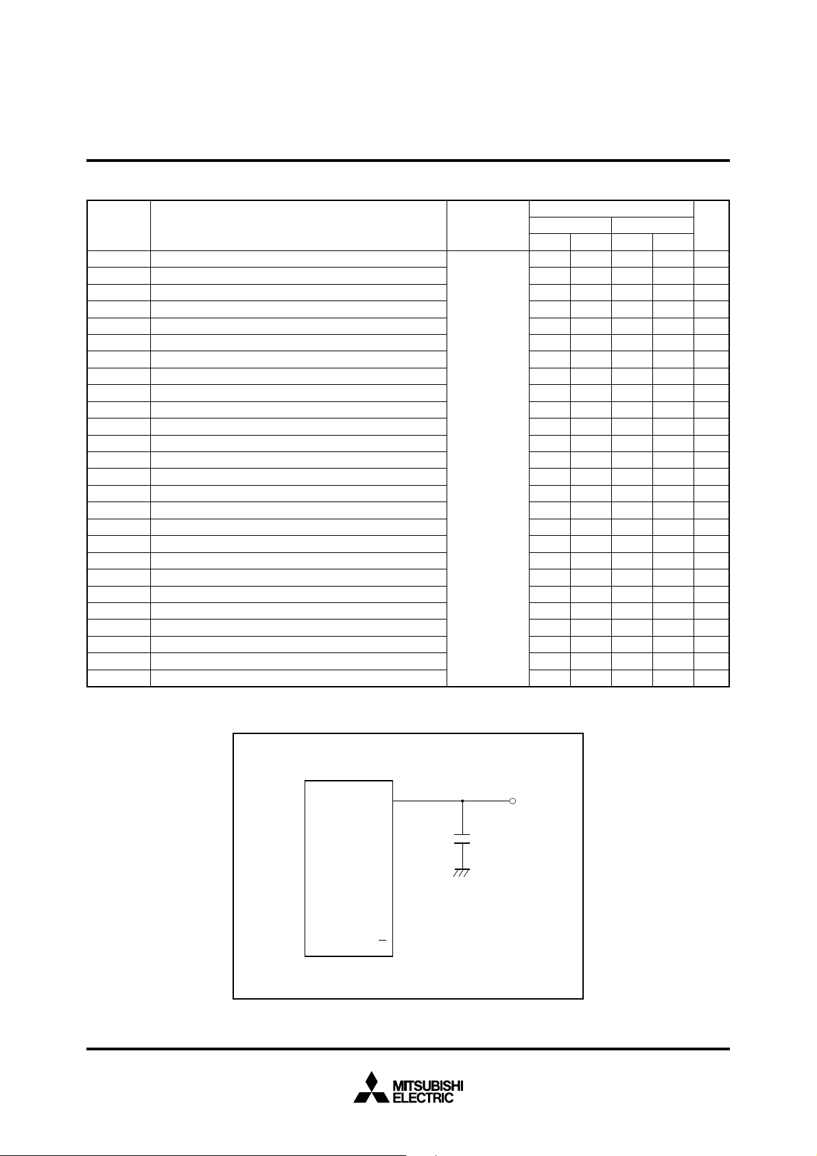
MITSUBISHI MICROCOMPUTERS
M37702M2AXXXFP, M37702M2BXXXFP
M37702S1AFP, M37702S1BFP
SINGLE-CHIP 16-BIT CMOS MICROCOMPUTER
Memory expansion mode and microprocessor mode (when wait bit = “0”, and external memory area accessed)
Limits
Symbol Parameter Unit
td(P0A–E)
td(E–P1Q)
tPXZ(E–P1Z)
td(P1A–E)
td(P1A–ALE)
td(E–P2Q)
tPXZ(E–P2Z)
td(P2A–E)
td(P2A–ALE)
td(φ1–HLDA)
td(ALE–E)
tw(ALE)
td(BHE–E)
td(R/W–E)
td(E–φ1)
th(E–P0A)
th(ALE–P1A)
th(E–P1Q)
tPZX(E–P1Z)
th(E–P1A)
th(ALE–P2A)
th(E–P2Q)
tPZX(E–P2Z)
th(E–BHE)
th(E–R/W)
tw(EL)
Port P0 address output delay time
Port P1 data output delay time (BYTE = “L”)
Port P1 floating start delay time (BYTE = “L”)
Port P1 address output delay time
Port P1 address output delay time
Port P2 data output delay time
Port P2 floating start delay time
Port P2 address output delay time
Port P2 address output delay time
_____
HLDA output delay time
ALE output delay time
ALE pulse width
____
BHE output delay time
__
R/W output delay time
1 output delay time
φ
Port P0 address hold time
Port P1 address hold time (BYTE = “L”)
Port P1 data hold time (BYTE = “L”)
Port P1 floating release delay time (BYTE = “L”)
Port P1 address hold time (BYTE = “H”)
Port P2 address hold time
Port P2 data hold time
Port P2 floating release delay time
____
BHE hold time
__
R/W hold time
_
E pulse width
Test conditions
Fig. 58
16 MHz 25 MHz
Min.
30
Max.
Min.
12
70
5
30
12
24
70
5
30
12
24
50
4
35
30
30
25
20
0
22
20
20
18
9
25
25
25
18
18
18
9
25
25
18
18
220
18
18
18
18
130
Max.
ns
45
ns
5
ns
ns
5
45
ns
ns
5
ns
ns
5
4
50
ns
ns
ns
ns
ns
ns
0
18
ns
ns
9
ns
ns
ns
ns
9
ns
ns
ns
ns
ns
ns
P 0
P 1
P 2
P 3
P 4
P 5
P 6
P 7
P 8
φ
1
E
Fig. 58 Testing circuit for ports P0–P8, φ1
100 pF
53
MITSUBISHI MICROCOMPUTERS
M37702M2AXXXFP, M37702M2BXXXFP
M37702S1AFP, M37702S1BFP
SINGLE-CHIP 16-BIT CMOS MICROCOMPUTER
TIMING DIAGRAM
Single-chip mode
f(XIN)
E
Port P0 output
Port P0 input
Port P1 output
Port P1 input
Port P2 output
Port P2 input
Port P3 output
Port P3 input
Port P4 output
Port P4 input
trt
f
t
c
t
su(P0D–E)
t
su(P1D–E)
t
su(P2D–E)
t
su(P3D–E)
t
su(P4D–E)
t
d(E–P0Q)
t
h(E–P0D)
t
d(E–P1Q)
t
h(E–P1D)
t
d(E–P2Q)
t
h(E–P2D)
t
d(E–P3Q)
t
h(E–P3D)
t
d(E–P4Q)
t
h(E–P4D)
t
w(H)
t
w(L)
Port P5 output
Port P5 input
Port P6 output
Port P6 input
Port P7 output
Port P7 input
Port P8 output
Port P8 input
54
t
su(P5D–E)
t
su(P6D–E)
t
su(P7D–E)
t
su(P8D–E)
t
d(E–P5Q)
t
h(E–P5D)
t
d(E–P6Q)
t
h(E–P6D)
t
d(E–P7Q)
t
h(E–P7D)
t
d(E–P8Q)
t
h(E–P8D)
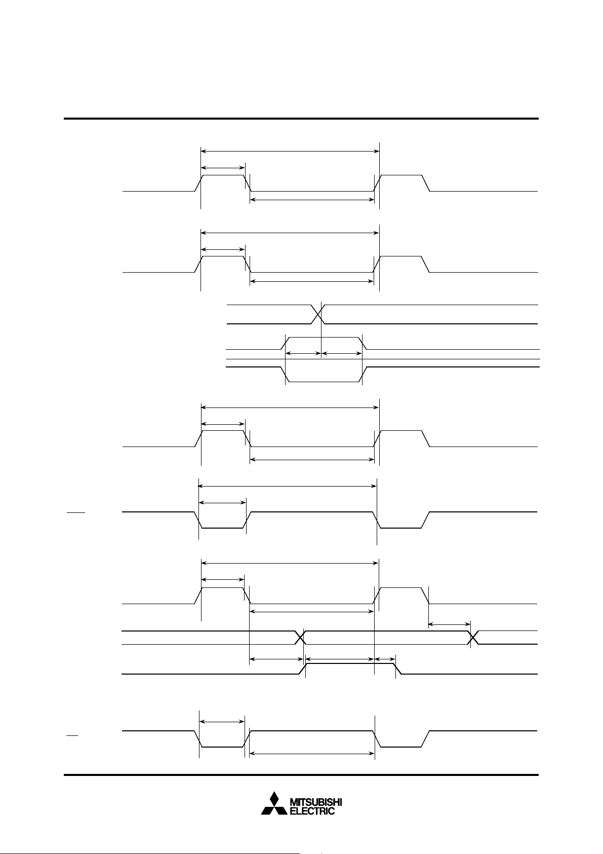
MITSUBISHI MICROCOMPUTERS
M37702M2AXXXFP, M37702M2BXXXFP
M37702S1AFP, M37702S1BFP
SINGLE-CHIP 16-BIT CMOS MICROCOMPUTER
t
c(TA)
t
w(TAH)
TAiIN input
t
w(TAL)
t
c(UP)
t
w(UPH)
OUT
input
TAi
t
w(UPL)
In Event counter mode
TBiIN input
AD
TRG
input
CLK
i
TAi
OUT
input
(Up-down input)
TAi
IN
input
(when count by falling)
TAi
IN
input
(when count by rising)
t
w(TBH)
t
t
w(CKH)
w(ADL)
t
h(TIN–UP)tsu(UP–TIN)
t
c(TB)
t
w(TBL)
t
c(AD)
t
c(CK)
t
w(CKL)
t
h(C–Q)
TxD
RxD
INTi
i
i
input
t
w(INL)
t
d(C–Q)
t
w(INH)
t
su(D–C)
t
h(C–D)
55

MITSUBISHI MICROCOMPUTERS
M37702M2AXXXFP, M37702M2BXXXFP
M37702S1AFP, M37702S1BFP
SINGLE-CHIP 16-BIT CMOS MICROCOMPUTER
Memory expansion mode and microprocessor mode
(When wait bit = “1”)
φ
1
E
RDY
input
( When wait bit = “0”)
φ
1
E
RDY
input
(When wait bit = “1” or “0” in common)
φ
1
t
su(HOLD–
φ
1
)
HOLD
input
t
su(RDY–
t
su(RDY–
φ
φ
1
)th(
1
)th(
φ
φ
1
–RDY)
1
–RDY)
th(φ
1
–HOLD)
56
HLDA
output
td(φ
Test conditions
CC
= 5 V ± 10%
• V
• Input timing voltage : V
• Output timing voltage : V
1
–HLDA)
IL
= 1.0 V, VIH = 4.0 V
OL =
0.8 V, VOH = 2.0 V
td(φ
1
–HLDA)

MITSUBISHI MICROCOMPUTERS
M37702M2AXXXFP, M37702M2BXXXFP
M37702S1AFP, M37702S1BFP
SINGLE-CHIP 16-BIT CMOS MICROCOMPUTER
Memory expansion mode and microprocessor mode (When wait bit = “1”)
t
tw(EL)
td(E-P1Q)
td(E-P2Q)
rtf tc
th(E-P0A)
th(E-P1Q)
th(E-P1A)
th(E-P2Q)
d(E- φ1)td(E- φ1)
t
td(P0A-E)
AddressAddress
tpxz(E-P1Z)
Address Address
td(P1A-E)
tsu(P1D-E) th(E-P1D)
tpxz(E-P2Z)
td(P2A-E)
tsu(P2D-E)
tpzx(E-P1Z)
tpzx(E-P2Z)
th(E-P2D)
f(XIN)
φ1
E
Port P0 output
(A
0 to A7)
Port P1 output
(A
8 to A15/D8 to D15)
(BYTE = “L”)
Port P1 output
(A
8 to A15)
(BYTE = “H”)
Port P1 input
Port P2 output
(A
16 to A23/D0 to D7)
Port P2 input
tw(H)tw(L)
th(ALE-P1A)
Address Data
td(P1A-ALE)
Address Address
th(ALE-P2A)
Address Data Address Address
td(P2A-ALE)
2 output
Port P3
(ALE)
Port P3
1 output
(BHE)
Port P30 output
(R/W)
tw(ALE)
td(BHE-E)
td(R/W-E)
Test conditions
• V
CC = 5 V ± 10%
• Output timing voltage : V
• Ports P1, P2 input : VIL = 0.8 V, VIH = 2.5 V
OL = 0.8 V, VOH = 2.0 V
td(ALE-E)
th(E-BHE)
th(E-R/W)
57

MITSUBISHI MICROCOMPUTERS
M37702M2AXXXFP, M37702M2BXXXFP
M37702S1AFP, M37702S1BFP
SINGLE-CHIP 16-BIT CMOS MICROCOMPUTER
Memory expansion mode and microprocessor mode (When wait bit = “0”, and external memory area is accessed)
c
t
f(XIN)
φ1
t
d(E- φ1)td(E- φ1)
td(P0A-E)
AddressAddress
tpxz(E-P1Z)
Address Address
td(P1A-E)
tsu(P1D-E) th(E-P1D)
tpxz(E-P2Z)
td(P2A-E)
tsu(P2D-E)
tpzx(E-P1Z)
tpzx(E-P2Z)
th(E-P2D)td(E-P2Q)
E
Port P0 output
0 to A7)
(A
Port P1 output
(A
8 to A15/D8 to D15)
(BYTE = “L”)
Port P1 output
(A
8 to A15)
(BYTE = “H”)
Port P1 input
Port P2 output
16 to A23/D0 to D7)
(A
Port P2 input
tw(EL)
th(E-P0A)
th(ALE-P1A)
Address Data
td(P1A-ALE)
Address Address
Address Data Address Address
td(P2A-ALE)
th(E-P1Q)
td(E-P1Q)
th(E-P1A)
th(E-P2Q)th(ALE-P2A)
2 output
Port P3
(ALE)
1 output
Port P3
(BHE)
Port P30 output
(R/W)
Test conditions
• V
CC = 5 V ± 10%
• Output timing voltage : V
• Ports P1, P2 input : V
tw(ALE)
td(BHE-E)
td(R/W-E)
OL = 0.8 V, VOH = 2.0 V
IL = 0.8 V, VIH = 2.5 V
td(ALE-E)
th(E-BHE)
th(E-R/W)
58

MITSUBISHI DATA BOOK
SINGLE-CHIP 16-BIT MICROCOMPUTERS Vol.1
Mar. First Edition 1996
Editioned by
Committee of editing of Mitsubishi Semiconductor Data Book
Published by
Mitsubishi Electric Corp., Semiconductor Division
This book, or parts thereof, may not be reproduced in any form without permission of
Mitsubishi Electric Corporation.
©1996 MITSUBISHI ELECTRIC CORPORATION Printed in Japan
 Loading...