
MITSUBISHI SEMICONDUCTOR
AMERICA, INC.
Preliminary
Single-Chip 8-BIT CMOS Microcontroller
M37640E8-XXXFP Specification
Ver 1.04

6/2/98
7600 Series
M37640E8-XXXF Preliminary Specification Mitsubishi Microcomputers
This publication, or any parts thereof, may not be reproduced in any form without the prior written
permission of Mitsubishi Semiconductor America, Inc. (MSAI).
The product(s) described in this publication are not designed, intended, or authorized for use as
components in systems intended for surgical implant into the body, or other applications intended to
support or sustain life, or for any other application in which failure of the product could create a
situation where personal injury or death may occur. Should Buyer purchase or use this product for any
such unintended or unauthorized application, Buyer shall indemnify and hold MSAI and its officers,
employees, subsidiaries, affiliates, and distributors harmless against all claims, costs, damages, and
expenses, and reasonable attorney fees arising out of, directly or indirectly, any claim of personal
injury or death associated with such unintended or unauthorized use, even if such claim alleges that
MSAI was negligent regarding the design and manufacture of the part.
Information supplied by MSAI is believed to be accurate and reliable. MSAI assumes no responsibility
for any errors that may appear in this publication. MSAI reserves the right, without notice, to make
changes in device design or specifications. Product is subject to availability.
©1997 Mitsubishi Semiconductor America, Inc.
Rev. 1.0 Internal Release April 2, 1997
Rev. 1.01 Design Spec Updates July 1, 1997
Rev. 1.02 Design Spec Updates August 28, 1997
Rev. 1.03 Internal Spec Updates Jan. 22, 1998
Rev. 1.04 Design Spec Updates June 2, 1998

7600 Series Mitsubishi
M37640E8-XXXFP Specification Semiconductor Corporation
1 Overview
1.1 MCU Features .................................................... 1-5
1.2 Pin Description and Layout................................ 1-6
2 Functional Description
2.1 Central Processing Unit......................................2-3
2.1.1 Register Structure......................................... 2-3
2.1.2 Accumulator (A)........................................... 2-3
2.1.3 Index Registers X and Y............................... 2-4
2.1.4 Stack Pointer................................................. 2-4
2.1.5 Program Counter .......................................... 2-4
2.1.6 Processor Status Register ............................. 2-5
2.2 CPU Mode Registers.......................................... 2-7
2.3 Oscillator Circuit................................................ 2-8
2.3.1 Description ................................................... 2-8
2.3.2 Frequency Synthesizer Circuit ................... 2-11
2.4 Memory Map.................................................... 2-14
2.4.1 Zero page.................................................... 2-15
2.4.2 Special Page................................................ 2-15
2.4.3 Special Function Registers .........................2-15
2.5 Processor Modes............................................... 2-17
2.5.1 Single Chip................................................. 2-17
2.5.2 Memory Expansion .................................... 2-18
2.5.3 Microprocessor........................................... 2-18
2.5.4 EPROM ...................................................... 2-18
2.5.5 Slow Memory Wait .................................... 2-19
2.5.6 Hold Function............................................. 2-23
2.5.7 Expanded Data Memory Access ................ 2-23
2.6 Peripheral Interface .......................................... 2-25
2.6.1 Chip Bus Timing ........................................ 2-25
2.6.2 Peripheral Interface and Access Timing..... 2-26
2.7 Input and Output Ports ..................................... 2-28
2.7.1 Ports............................................................ 2-28
2.7.1.1 I/O Ports................................................ 2-29
2.7.1.2 Power and Ground Pins........................ 2-40
2.7.1.3 CNVss Pin............................................. 2-40
2.7.1.4 Xin and Xout Pins.................................2-40
2.7.1.5 X
Cin
and XCout Pins ............................ 2-40
2.7.1.6 RESET Pin............................................ 2-40
2.7.1.7 RDY Pin ............................................... 2-41
2.7.1.8 DMAout Pin ......................................... 2-41
2.7.1.9 F
out
Pin.................................................. 2-41
2.7.1.10 SYNC
out
Pin....................................... 2-41
2.7.1.11 RD and WR Pins................................. 2-41
2.7.1.12 LPF Pin............................................... 2-41
2.7.1.13 USB D+/D- Pins................................. 2-41
2.7.1.14 Ext. Cap Pin........................................ 2-41
2.7.2 Port Control Register.................................. 2-42
2.7.3 Port 2 Pull-up Control Register.................. 2-42
2.8 Interrupt Control Unit....................................... 2-43
2.8.1 Interrupt Control......................................... 2-43
2.8.2 Interrupt Sequence and Timing ..................2-47
2.9 Universal Serial Bus......................................... 2-49
2.9.1 USB Function Control Unit (USB FCU).... 2-50
2.9.1.1 Serial Interface Engine ......................... 2-50
2.9.1.2 Generic Function Interface...................2-50
2.9.1.3 Serial Engine Interface Unit .................2-50
2.9.1.4 Microcontroller Interface Unit.............. 2-50
2.9.1.5 USB Transceiver................................... 2-50
2.9.2 USB Interrupts............................................2-51
2.9.2.1 USB Function Interrupt ........................2-51
2.9.2.2 USB SOF Interrupt...............................2-52
2.9.3 USB Endpoint FIFOs.................................. 2-52
2.9.3.1 IN (Transmit) FIFOs............................. 2-52
2.9.3.2 Out (Receive) FIFOs............................. 2-53
2.9.4 USB Special Function Registers................. 2-54
2.10 Master CPU Bus Interface.............................. 2-65
2.10.1 Data Bus Buffer Status Registers
(DBBS0, DBBS1)....................................... 2-68
2.10.2 Input Data Bus Buffer Registers
(DBBIN0, DBBIN1)................................... 2-68
2.10.3 Output Data Bus Buffer Registers
(DBBOUT0, DBBOUT1)........................... 2-68
2.11 Direct Memory Access Controller.................. 2-69
2.11.1 Operation.................................................. 2-70
2.11.1.1 Source, Destination, and Transfer Count
Register Operation............................................ 2-71
2.11.1.2 DMAC Transfer Request Sources......2-71
2.11.1.3 Transfer Features for USB and MBI .. 2-72
2.11.1.4 DMAC Transfer Mode ....................... 2-74
2.11.1.5 DMAC Transfer Timing..................... 2-74
2.12 Special Count Source Generator .................... 2-79
2.12.1 SCSG Operation....................................... 2-79
2.12.2 SCSG Description..................................... 2-80
2.12.2.1 SCSG1 ................................................2-80
2.12.2.2 SCSG2 ................................................2-80
2.13 Timers............................................................. 2-82
2.13.1 Timer X..................................................... 2-82
2.13.1.1 Read and Write Method...................... 2-82
2.13.1.2 Count Stop Control............................. 2-83
2.13.1.3 Timer Mode........................................2-83
2.13.1.4 Pulse Output Mode.............................2-83
2.13.1.5 Event Counter Mode........................... 2-84
2.13.1.6 Pulse Width Measurement Mode........ 2-84
2.13.2 Timer Y..................................................... 2-84
2.13.2.1 Read and Write Method...................... 2-85
2.13.2.2 Count Stop Control............................. 2-85
2.13.2.3 Timer Mode........................................2-85
2.13.2.4 Pulse Period Measurement Mode....... 2-86
2.13.2.5 Event Counter Mode........................... 2-86
2.13.2.6 HL Pulse-width Measurement Mode.. 2-86
2.13.3 Timer 1 ..................................................... 2-87
2.13.3.1 Timer Mode........................................2-87
2.13.3.2 Pulse Output Mode.............................2-87
2.13.4 Timer 2 ..................................................... 2-88
2.13.4.1 Timer Mode........................................2-88
2.13.4.2 Pulse Output Mode.............................2-88

Mitsubishi 7600 Series
Semiconductor Corporation M37640E8-XXXFP Specification
2.13.5 Timer 3 ..................................................... 2-88
2.13.5.1 Timer Mode ........................................2-88
2.14 UART .............................................................2-90
2.14.1 Baud Rate Selection.................................. 2-91
2.14.2 UART Mode Register............................... 2-93
2.14.3 UART Control Register............................2-94
2.14.4 UART Baud Rate Register .......................2-94
2.14.5 UART Status Register ..............................2-94
2.14.6 Transmit/Receive Format .........................2-96
2.14.7 Interrupts................................................... 2-98
2.14.8 Clear-to Send (CTSx) and
Request-to-Send (RTSx) Signals................2-99
2.14.9 UART Address Mode.............................2-100
2.15 Serial I/O ...................................................... 2-102
2.15.1 SIO Control Register ..............................2-102
2.15.2 SIO Operation.........................................2-102
2.16 Low Power Modes........................................ 2-105
2.16.1 Stop Mode............................................... 2-105
2.16.2 Wait Mode.............................................. 2-106
2.17 Reset .............................................................2-107
2.18 Key-On Wake-Up......................................... 2-108
3 Electrical Characteristics
3.1 Absolute Maximum Ratings...............................3-3
3.2 Recommended Operating conditions ................. 3-4
3.3 Electrical Characteristics.................................... 3-6
3.4 Timing Requirements and
Switching Characteristics.................................... 3-8
4 Application Notes
4.1 DMAC................................................................ 4-3
4.1.1 Application ...................................................4-3
4.2 UART .................................................................4-4
4.2.1 Application ...................................................4-4
4.3 Timer ..................................................................4-5
4.3.1 Usage ............................................................4-5
4.4 Frequency Synthesizer Interface ........................4-6
4.5 USB Transceiver ................................................ 4-7
4.6 Ports....................................................................4-8
4.7 Programming Notes............................................4-9
5 Register List

MITSUBISHI SEMICONDUCTOR
AMERICA, INC.
PRELIMINARY
Chapter 1
PRODUCT
DESCRIPTION
1 Overview . . . . . . . . . . . . . . . . . .1-3
1.1 MCU Features . . . . . . . . . . . .1-5
1.2 Pin Description and Layout . . 1-6

1-2 6/2/98
7600 Series
M37640E8-XXXF Preliminary Specification Mitsubishi Microcomputers
7600 Series
Mitsubishi Microcomputer M37640E8-XXXF Preliminary Specification
6/2/98 1-3
1 Overview
The 7600 series, an enhanced family of CMOS 8-bit microcontrollers, offers high-speed operation at
low voltage, large internal-memory options, and a wide variety of standard peripherals. The series is
code compatible with the M38000, M37200, M37400, and the M37500 series, and provides many
performance enhancements to the instruction set.
This device is a single chip PC peripheral microcontroller based on the Universal Serial Bus (USB)
Version 1.0 specification. This device provides data exchange between a USB-equipped host computer
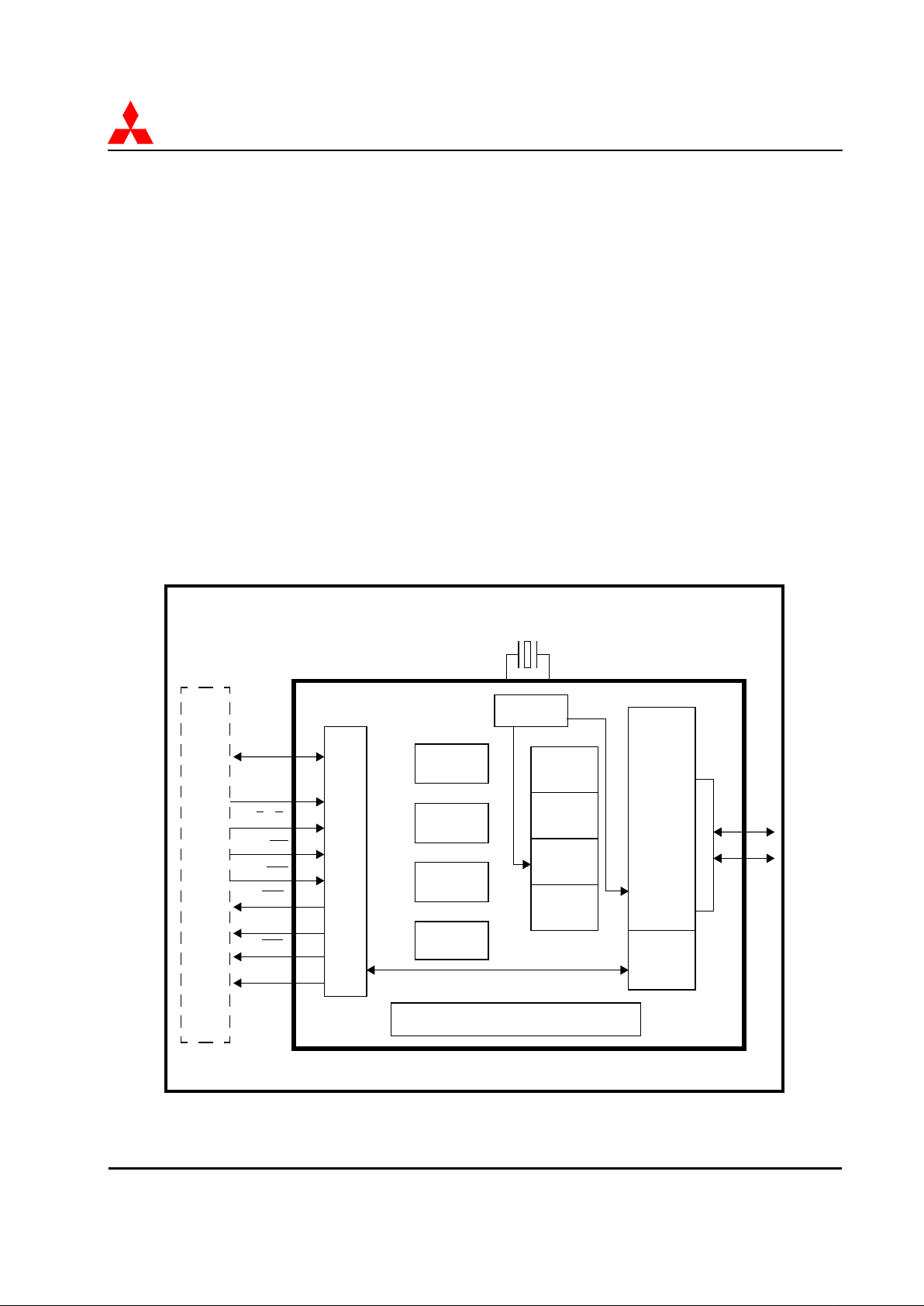
and PC peripherals such as telephones, audio systems and digital cameras. See Figure 1-1 for an
application system diagram.
The USB function control unit can support all four data transfer types listed in the USB specification:
Control, Isochronous, Interrupt, and Bulk. Each transfer type is used for controlling a different set of
PC peripherals. Isochronous transfers provide guaranteed bus access, a constant data rate, and error
tolerance for devices such as computer-telephone integration (CTI) and audio systems. Interrupt transfers
are designed to support human input devices (HID) that communicate small amounts of data
infrequently. Bulk transfers are necessary for devices such as digital cameras and scanners that
communicate large amounts of data to the PC as bus bandwidth becomes free. Finally, control transfers
are supported and are useful for bursty, host-initiated type communication where bus management is the
primary concern.
Figure 1-1. Application System Diagram
frequency
RAM(1K)
ROM(32K)
DMAC x 2
7600 CPU
UART x 2
Timers
SIO
SCSG
I/O Ports (P0 ~ P8)
Bus Interface Control Block
FIFOs
USB Function Control Unit
Transceiver
D+
D-
(Normal MCU or DMA Transfer)
4-24 MHz
DQ(7:0)
S
0
, S
1
RD
WR
IBF
0
OBF
0
48 MHz
Φ
Master CPU
IBF
1
OBF
1
A
0
synthesizer

1-4 6/2/98
7600 Series
M37640E8-XXXF Preliminary Specification Mitsubishi Microcomputers
Table 1-1. Device Feature List
Parameter Function Description
Number of basic instructions 71
Instruction execution time (minimum) 83ns at Φ = 12 MHz (setting Φ to less than 5MHz is NOT recommended)
Clock frequency (maximum) Xin = 48 MHz, XC
in
= 5 MHz (square wave), Φ= 12 MHz
Clock multiplier option
External clock X
in
and XCin can be selectively divided and multiplied by X to create
system internal clock Φ
Memory size
ROM 32K bytes
RAM 1K bytes
Input/Output ports
P0~P3, P5, P6,
P8
I/O 8-bit X 7 (Port 2 has a key-on wake-up feature)
P4, P7 I/O 5-bit X 2
USB Function Control
FIFO:
Endpoint 0: IN 16-byte OUT 16-byte
Endpoint 1: IN 512-byteOUT 800-byte
Endpoint 2: IN 32-byte OUT 32-byte
Endpoint 3: IN 16-byte OUT 16-byte
Endpoint 4: IN 16-byte OUT 16-byte
Master CPU bus interface
DQ(7:0),
R(E), W(R/W), S0, S1, A0, IBF0, OBF0, IBF1, OBF1; total of 17 signals interface
with master CPU (Intel 8042-like interface)
Special Count Source Generator(SCSG) Baud rate synthesizer
UART X 2 7/8/9-bit character length, with
CTS, RTS available
Serial I/O 8-bit clock synchronous serial I/O, supports both master and slave modes
Timers 8-bit X 3, 16-bit X 2
DMAC 2 channels, 16 address lines, support single byte or burst transfer modes
Software selectable slew rate control Ports P0 ~ P8
Interrupts 4 external, 19 internal, 1 software, 1 system interrupts
Supply voltage V
cc
= 4.15 ~ 5.25V
External memory expansion Memory Expansion and Microprocessor mode
External Data Memory Access (EDMA) Allows > 64 Kbyte data access for instruction LDA (indY) and STA (indY)
Device structure CMOS
Package 80P6N
Operating temperature range -20 to 85
o
C

7600 Series
Mitsubishi Microcomputer M37640E8-XXXF Preliminary Specification
MCU Features 6/2/98 1-5
1.1 MCU Features
• 7600 8-bit CPU core, CMOS process
• Minimum instruction execution time of 83ns (1-cycle instruction @ Φ = 12 MHz)
• Efficient software support (C and/or Assembly)
• ROM: 32 KB on-chip
• RAM: 1 KB on-chip
• Built-in Microprocessor or Memory-expansion modes
• Three slow memory wait modes: Software Wait, RDY Wait, and Extended RDY Wait
• Nine I/O Ports, total 66 programmable I/O pins available
• Programmable direction control on every I/O pin
• Software selectable slew rate control on every I/O pin
• Master CPU Bus Interface:
• MCU can be operated in slave mode by control signals from the host CPU
• 8 data lines (DQ7-DQ0) and R(E), W(R/W), A0, S0, S1, IBF0, OBF0, IBF1, OBF1 signals
available
• Master CPU sends and receives data, command, and status by means of DQ7-DQ0
• USB Function Control Unit
• USB Transceiver (conforms to USB V1.0 Specification)
• DMA Controller:
• Two DMA channels available
• 16 address lines for 64K byte address space
• Single byte or burst transfer modes
• Transfer request by external pins, software triggers or built-in peripherals
• Maximum 6M byte/sec transfer speed (in burst mode)
• Timers: three 8-bit timers and two 16-bit timers available
• Two full duplex UARTs available
• One master/slave clock synchronous I/O (SIO), internal or external clock selectable
• Built-in Special Count Source Generator (SCSG): can be a clock source for Timer X, UARTs,
and SIO
• Power-saving wait (IDLE) and stop (powerdown) modes.
1-6 6/2/98 Pin Description and Layout
7600 Series
M37640E8-XXXF Preliminary Specification Mitsubishi Microcomputers
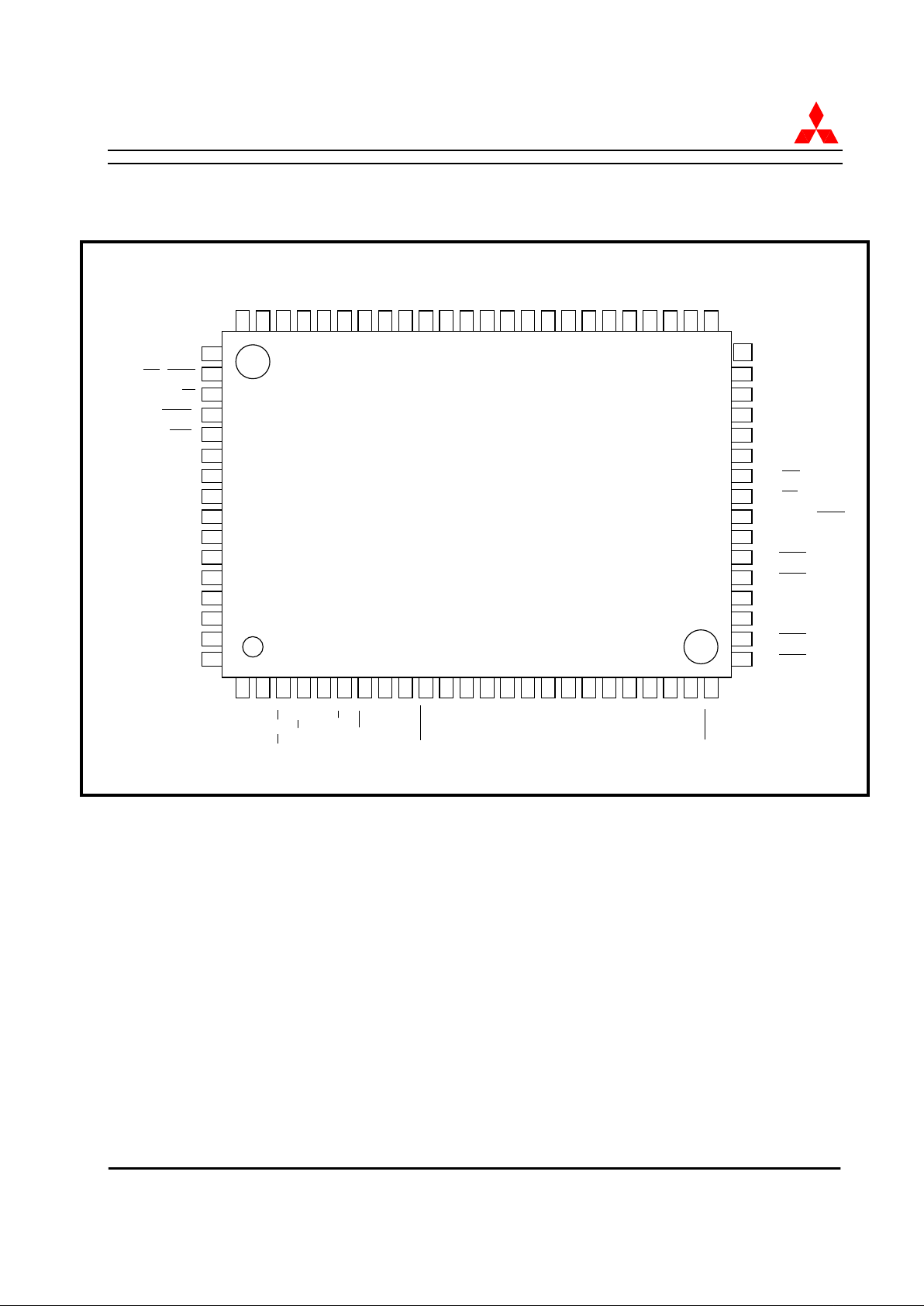
1.2 Pin Description and Layout
Figure 1-2. Pin Layout
P30/[RDY]P74/OBF
1
P4
0
/[EDMA]
41
40
24
65
P73/IBF1/HLDA66
P72/S1
67
P71/(HOLD) 68
P70/(SOF) 69
USB D+
70
USB D-
71
Ext. Cap
72
V
ss
73
V
cc
74
P67/DQ7
75
P66/DQ6
76
P65/DQ5
77
P64/DQ4
78
P63/DQ3
79
P62/DQ2
80
P4
1
/INT0
23
P4
2
/INT1
22
P4
3
/CNTR0
21
P4
4
/CNTR1
20
LPF
19
AV
ss
18
AV
cc
17
V
cc
16
X
out
15
X
in
14
V
ss
13
P5
0
/XC
in
12
P5
1
/T
out
/XC
out
11
RESET
10
CNV
ss
9
P5
2
/OBF
0
8
P5
3
/IBF
0
7
P5
4
/S
0
6
P5
5
/A
0
5
P5
6
/R(E)
4
P5
7
/W(R/W)
3
P6
0
/DQ0
2
P6
1
/DQ1
1
P3
1
39
P3
2
38
P33/[DMA
out
]37
P34/[Φ
out
]36
P35/[SYNC
out
]35
P36/[WR]34
P37/[RD]33
P80/UTXD2/SRDY32
P81/URXD2/SCLK31
P82/CTS2/SRXD30
P83/RTS2/STXD29
P84/UTXD128
P85/URXD127
P86/CTS126
P87/RTS125
42
43
44
45
46
47
48
49
50
51
52
53
54
55
56
57
58
59
60
61
62
63
64
P1
7
/[AB15]
P1
6
/[AB14]
P1
5
/[AB13]
P1
4
/[AB12]
P1
3
/[AB11]
P1
2
/[AB10]
P1
1
/[AB9]
P1
0
/[AB8]
P0
7
/[AB7]
P0
6
/[AB6]
P0
5
/[AB5]
P0
4
/[AB4]
P0
3
/[AB3]
P0
2
/[AB2]
P0
1
/[AB1]
P0
0
/[AB0]
P2
7
/[DB7]
P2
6
/[DB6]
P2
5
/[DB5]
P2
4
/[DB4]
P2
3
/[DB3]
P2
2
/[DB2]
P2
1
/[DB1]
P2
0
/[DB0]
M37640E8-XXXFP
[ ]Indicates function in memory expansion and microprocessor modes
7600 Series
Mitsubishi Microcomputer M37640E8-XXXF Preliminary Specification
Pin Description and Layout 6/2/98 1-7
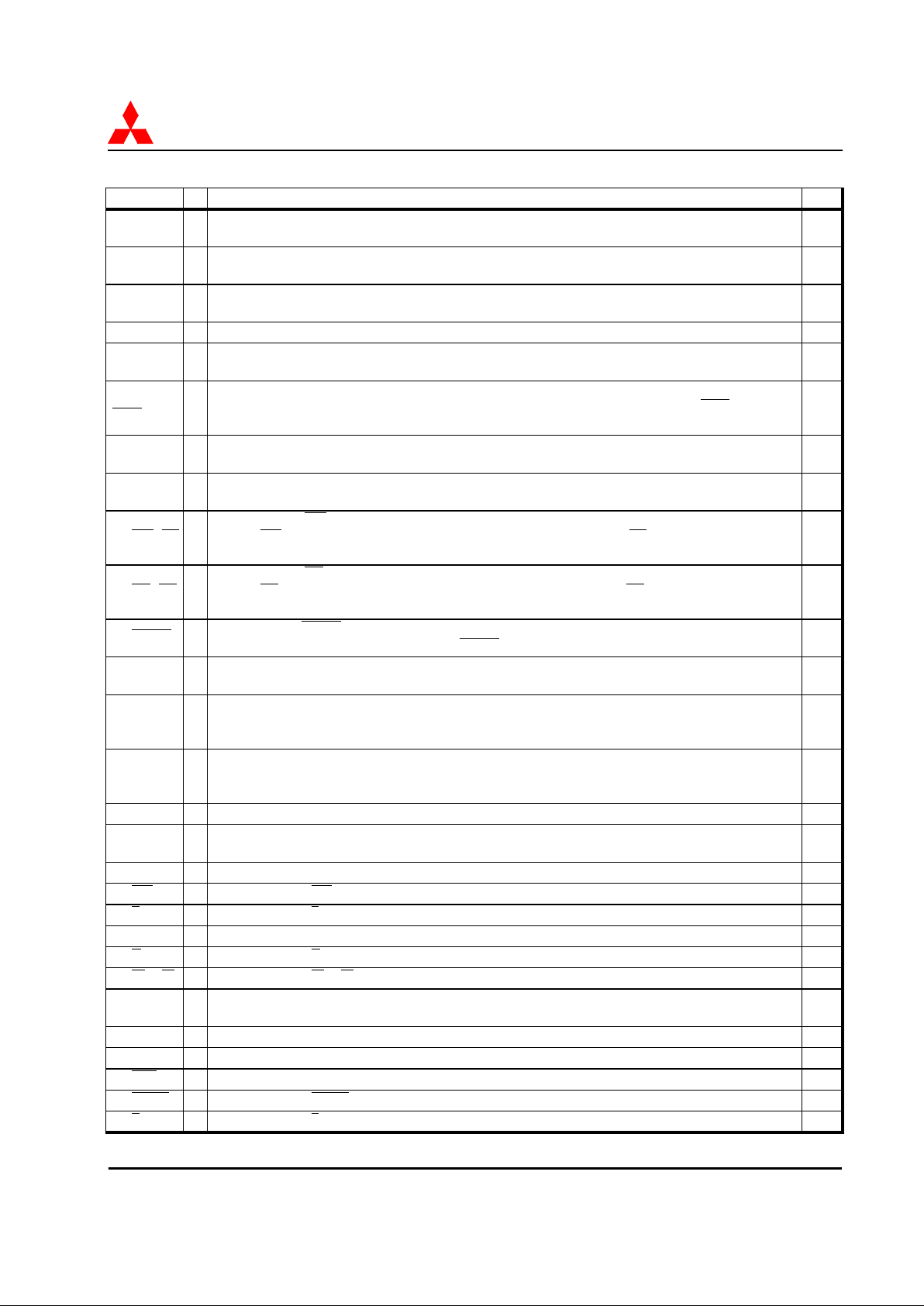
Table 1-2. Pin Description
Name I/O Description Pin #
P0
0
/AB0
~ P1
7
/AB15
I/O
CMOS I/O port (address bus). When the MCU is in memory expansion or microprocessor mode, these pins
function as the address bus.
56-41
P2
0
/DB0
~ P2
7
/DB7
I/O
CMOS I/O port (data bus). When the MCU is in memory expansion or microprocessor mode, these pins
function as the data bus. These pins may also be used to implement the Key-on Wake up function.
64-57
P3
0
/RDY I/O
CMOS I/O port (Ready). When the MCU is in memory expansion or microprocessor mode, this pin functions
as RDY (hardware wait cycle control).
40
P3
1
I/O CMOS I/O port. 39
P3
2
/(VRFY) I/O
CMOS I/O port. When the MCU is in EPROM program mode, the pin is used as VRFY (EPR OM memory
verify).
38
P3
3
/DMA
out
/PGM
I/O
CMOS I/O port (DMA
out
). When the MCU is in memory expansion or microprocessor mode, this pin is set to a
“1” during a DMA transfer. When the MCU is in EPROM program mode, the pin is used as
PGM (EPROM
memory program).
37
P3
4/Φout
I/O
CMOS I/O port (Φ). When the MCU is in memory expansion or microprocessor mode, this pin becomes Φ
out
pin.
36
P3
5
/SYNC
out
I/O
CMOS I/O port (SYNC output). When the MCU is in memory expansion or microprocessor mode, this pin
becomes the SYNCout pin.
35
P3
6
/WR/(CE) I/O
CMOS I/O port. (
WR output). When the MCU is in memory expansion or microprocessor mode, this pin
becomes
WR. When the MCU is in EPROM program mode, the pin is used as CE (EPR OM memory chip
enable).
34
P37/RD/(OE) I/O
CMOS I/O port. (
RD output). When the MCU is in memory expansion or microprocessor mode, this pin
becomes
RD. When the MCU is in EPROM program mode, the pin is used as OE (EPROM memory output
enable).
33
P4
0
/EDMA I/O
CMOS I/O port (
EDMA: Expanded Data Memory Access). When the MCU is in memory expansion or
microprocessor mode, this pin can become the
EDMA pin.
24
P4
1
/INT0
~ P4
2
/INT1
I/O
CMOS I/O port or external interrupt ports INT0 and INT1. These external interrupts can be configured to be
active high or low.
23-22
P4
3
/CNTR0 I/O
CMOS I/O port or Timer X input pin for pulse width measurement mode and event counter mode or Timer X
output pin for pulse output mode. This pin can also be used as an external interrupt when Timer X is not in
output mode. The interrupt polarity is selected in the Timer X mode register.
21
P44/CNTR1 I/O
CMOS I/O port or Timer Y input pin for pulse period measurement mode, pulse H-L measurement mode and
event counter mode or Timer Y output pin for pulse output mode. This pin can also be used as an external
interrupt when Timer Y is not in output mode. The interrupt polarity is selected in the Timer Y mode re gister.
20
P5
0
/XC
in
I/O CMOS I/O port or XCin. 12
P5
1/Tout
/
XC
out
I/O CMOS I/O port or Timer 1/2 pulse output pin (can be configured initially high or initially low), or XC
out
.11
P5
2
/OBF0I/O CMOS I/O port or OBF0 output to master CPU for data bus buffer 0. 8
P5
3
/IBF
0
I/O CMOS I/O port or IBF0 output to master CPU for data bus buffer 0. 7
P5
4/S0
I/O CMOS I/O port or S0 input from master CPU for data bus buffer 0. 6
P5
5/A0
I/O CMOS I/O port or A0 input from master CPU. 5
P5
6
/R(E) I/O CMOS I/O port or R(E) input from master CPU. 4
P5
7
/W(R/W) I/O CMOS I/O port or W(R/W) input from master CPU. 3
P6
0
/DQ0
~ P6
7
/DQ7
I/O CMOS I/O port or master CPU data bus.
2-1,
80-75
USB D
-
I/O USB D- voltage line interface, a series resistor of 33 Ω should be connected to this pin. (see note) 71
USB D
+
I/O USB D+ voltage line interface, a series resistor of 33 Ω should be connected to this pin. (see note) 70
P7
0
/SOF I/O CMOS I/O port or USB start of frame pulse output, an 80 ns pulse outputs on this pin for every USB frame. 69
P7
1
/HOLD I/O CMOS I/O port or HOLD pin. 68
P7
2/S1
I/O CMOS I/O port or S1 input from master CPU for data bus buffer 1. 67

1-8 6/2/98 Pin Description and Layout
7600 Series
M37640E8-XXXF Preliminary Specification Mitsubishi Microcomputers
D+/D- Line driver notes: In order to match the USB cable impedance, a series resistor of 33Ω, 1%,
1/8 W should be connected to each USB line; i.e. on D+ (pin 70) and on D- (pin 71). Also, a
coupling capacitor with the recommended value of 33pF should be connected between D+ and D- after
the 33Ω series resistors. If the USB line is improperly terminated or not matched, signal fidelity will
suffer, resulting in excessive overshoot or undershoot. This will potentially introduce bit errors.
VDD/VSS notes: In order to reduce the effects of the inductance of the traces on the board,
decoupling capacitors should be connected between pins 73(VSS) and 74(VDD), 13(VSS) and 16(VDD),
and 17(AVDD) and 19(AVSS). Recommended values are a 4.7 µF in parallel with a 0.1 µF.
Figure 1-3. VDD/VSS decoupling capacitor connections
P7
3
/IBF1/
HLDA
I/O
CMOS I/O port or
IBF1 output to master CPU for data bus buffer 1, orHLDA pin. IBF1 and HLDA are
mutually exclusive.
IBF1 has priority over HLDA.
66
P7
4
/OBF1I/O CMOS I/O port or OBF1 output to master CPU for data bus buffer 1. 65
P8
0
/UTXD2/
SRDY
I/O
CMOS I/O port or UAR T2 pin UTXD2 or SIO pin
SRDY. UART2 and SIO are mutually exclusive, UAR T2 has
priority over SIO.
32
P8
1
/URXD2/
SCLK
I/O
CMOS I/O port or UART2 pin URXD2 or SIO pin SCLK. UART2 and SIO are mutually exclusive, UAR T2
has priority over SIO.
31
P8
2
/CTS2/
SRXD
I/O
CMOS I/O port or UART2 pin CTS2 or SIO pin SRXD. UART2 and SIO are mutually exclusive, UAR T2 has
priority over SIO.
30
P8
3
/RTS2/
STXD
I/O
CMOS I/O port or UART2 pin RTS2 or SIO pin STXD. UART2 and SIO are mutually exclusive, UART2 has
priority over SIO.
29
P8
4
/UTXD1 I/O CMOS I/O port or UART1 pin UTXD1. 28
P8
5
/URXD1 I/O CMOS I/O port or UART1 pin URXD1. 27
P8
6/
CTS1 I/O CMOS I/O port or UART1 pin CTS1. 26
P8
7
/RTS1 I/O CMOS I/O port or UART1 pin RTS1. 25
AV
cc
,AV
ss
I Power supply inputs for analog circuitry AVcc = 4.15~ 5.25V, A Vss = 0V 17,19
CNV
ss
I
Controls the processor mode of the chip. Normally connected to V
ss
or Vcc. When the MCU is in EPROM
program mode, this pin supplies the programming voltage to the EPROM.
9
V
cc,Vss
I Power supply inputs: Vcc = 4.15~ 5.25V, Vss = 0V
16/74,
13/73
RESET I
T o enter the reset state, this pin must be k ept L for more that 2µs (20Φ cycles under normal V
cc
conditions). If
the crystal or ceramic resonator requires more time to stabilize, extend this L level time appropriately.
10
XC
in
XC
out
IOAn external ceramic or quartz crystal oscillator can be connected between the XCin and XC
out
pins. If an
external clock source is used, connect the clock source to the XC
in
pin and leave the XC
out
pin open.
12
11
X
in
X
out
I
O
Input and output signals to and from the internal clock generation circuit. Connect a ceramic resonator or quartz
crystal between X
in
and X
out
pins to set the oscillation frequency. If an e xternal clock is used, connect the clock
source to the X
in
pin and leave the X
out
pin open.
14
15
LPF O Loop filter for the frequency synthesizer. 18
Ext. Cap I
An external capacitor (Ext. Cap) pin. When the USB transceiver voltage converter is used, a 2µf or larger
capacitor should connect between this pin and V
ss
to ensure proper operation of the USB line driver. The
voltage converter is enabled by setting bit 4 of the USB control register (0013
16
) to a “1”.
72
Table 1-2. Pin Description
Name I/O Description Pin #
C1 C2
Pin 73
Pin 74
(VDD)
(VSS)
C1 C2
Pin 13
Pin 16
(VDD)
(VSS)
C1 C2
Pin 17
Pin 19
(A
VDD)
(AVSS)
C1 = 4.7 µF
C2 = 0.1 µF

MITSUBISHI SEMICONDUCTOR
AMERICA, INC.
PRELIMINARY
Chapter 2
Functional
Description
2.1 Central Processing Unit . . . . . .2-3
2.2 CPU Mode Registers . . . . . . . .2-7
2.3 Oscillator Circuit . . . . . . . . . . . .2-8
2.4 Memory Map. . . . . . . . . . . . . .2-14
2.5 Processor Modes . . . . . . . . . .2-17
2.6 Peripheral Interface. . . . . . . . .2-25
2.7 Input and Output P orts. . . . . .2-28
2.8 Interrupt Control Unit . . . . . . .2-43
2.9 Universal Serial Bus . . . . . . . .2-49
2.10 Master CPU Bus Interface . .2-65
2.11 Direct Memory Access
Controller . . . . . . . . . . . . . 2-69
2.12 Special Count Source
Generator . . . . . . . . . . . . . 2-79
2.13 Timers . . . . . . . . . . . . . . . . . .2-82
2.14 U ART . . . . . . . . . . . . . . . . . . .2-90
2.15 Serial I/O . . . . . . . . . . . . . . .2-102
2.16 Low Po wer Modes . . . . . . .2-105
2.17 Reset . . . . . . . . . . . . . . . . . .2-107
2.18 K e y-On Wak e-Up . . . . . . . .2-108

2-2 7/9/98
7600 Series
M37640E8-XXXF Preliminary Specification Mitsubishi Microcomputers
7600 Series
Mitsubishi Microcomputer M37640E8-XXXF Preliminary Specification
Central Processing Unit 7/9/98 2-3
2 Functional Description
2.1 Central Processing Unit
The central processing unit (CPU) has six registers:
• Accumulator (A)
• Index Register X (X)
• Index Register Y (Y)
• Stack Pointer (S)
• Processor Status Register (PS)
• Program Counter (PC)
2.1.1 Register Structure
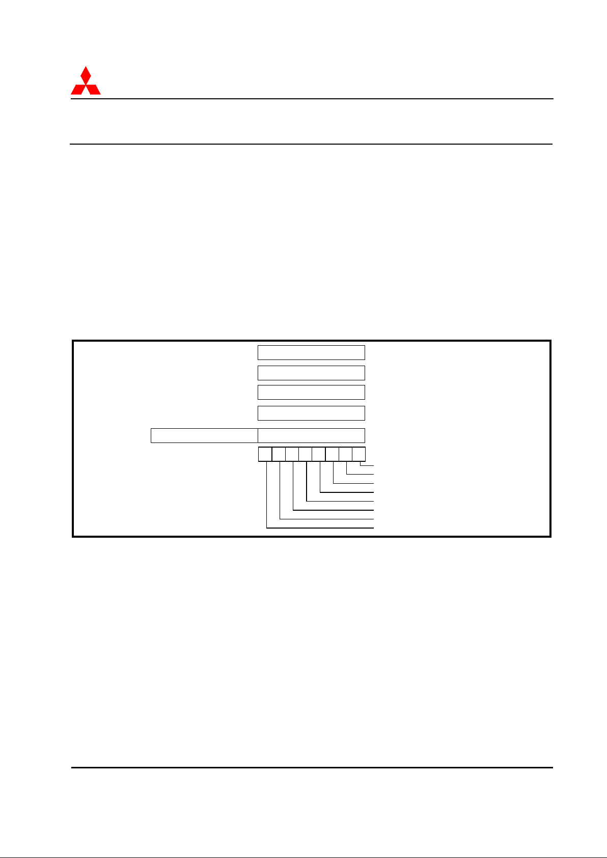
Figure 2-1. Register Structure
Five of the CPU registers are 8-bit registers. These are the Accumulator (A), Index register X (X),
Index register Y (Y), Stack pointer (S), and the Processor Status register (PS).
The Program counter (PC) is a 16-bit register consisting of two 8-bit registers (PCH and PCL) (see
Figure 2-1.).
After a hardware reset, bit 2 (the I flag) of the PS is set high and the values at the addresses FFFA
16
and FFFB16 are stored in the PC, but the values of the other bits of the PS and the other registers are
undefined. Initialization of undefined registers may be necessary for some programs.
2.1.2 Accumulator (A)
The accumulator is the main register of the microcomputer. Data operations such as data transfer, input/
output, and so forth, are executed mainly through the accumulator.
07
Accumulator
07
Index Register X
07
Index Register Y
07
Stack Pointer
07
PCL
15
PCH
07
Carry Flag (bit 0)
Zero Flag (bit 1)
Interrupt Disable Flag (bit 2)
Decimal Mode Flag (bit 3)
Break Flag (bit 4)
Index X Mode Flag (bit 5)
Overflow Flag (bit 6)
Negative Flag (bit 7)
Program Counter
D I Z CN V T B
Processor Status Register

2-4 7/9/98 Central Processing Unit
7600 Series
M37640E8-XXXF Preliminary Specification Mitsubishi Microcomputers
2.1.3 Index Registers X and Y
Both index registers X and Y are 8-bit registers. In the absolute addressing modes, the contents of
these registers are added to the value of the OPERAND to specify the real address.
In the indirect X addressing mode, the value of the OPERAND is added to the contents of register X
to specify the zero page basic address. The data at the basic address specifies the real address.
In the indirect Y addressing mode, the value of the operand specifies a zero page address. The data at
this address is added to the contents of register Y to produce the real address. These addressing modes
are useful for referencing subroutine tables and memory tables.
When the T flag in the processor status register is set high, the value contained in index register X points
to a zero page memory location that replaces the accumulator for most accumulator based instructions.
2.1.4 Stack Pointer
The stack pointer is an 8-bit register used during subroutine calls and interrupts. The stack is used to
store the current address data and processor status when branching to subroutines or interrupt routines.
The lower eight bits of the stack address are determined by the contents of the stack pointer. The
upper eight bits of the stack address are determined by the Stack Page Select Bit, bit 2 of the CPU
Mode Register A. If the Stack Page Select bit is “0”, then the RAM in the zero page (addresses
007016 to 00FF16) is used as the stack area. If the stack page select bit is “1” (the default value), then
the RAM in one page (addresses 010016 to 01FF16) is used as the stack area. The base of the stack
must be set in software, and stack grows towards lower addresses from that point. The operations of
pushing register contents onto the stack and popping them from the stack are shown in Figure 2-2.
2.1.5 Program Counter
The program counter (PC) is a 16-bit register consisting of two 8-bit sub-registers PCH and PCL. It is
used to indicate the address of the next instruction to be executed.
7600 Series
Mitsubishi Microcomputer M37640E8-XXXF Preliminary Specification
Central Processing Unit 7/9/98 2-5
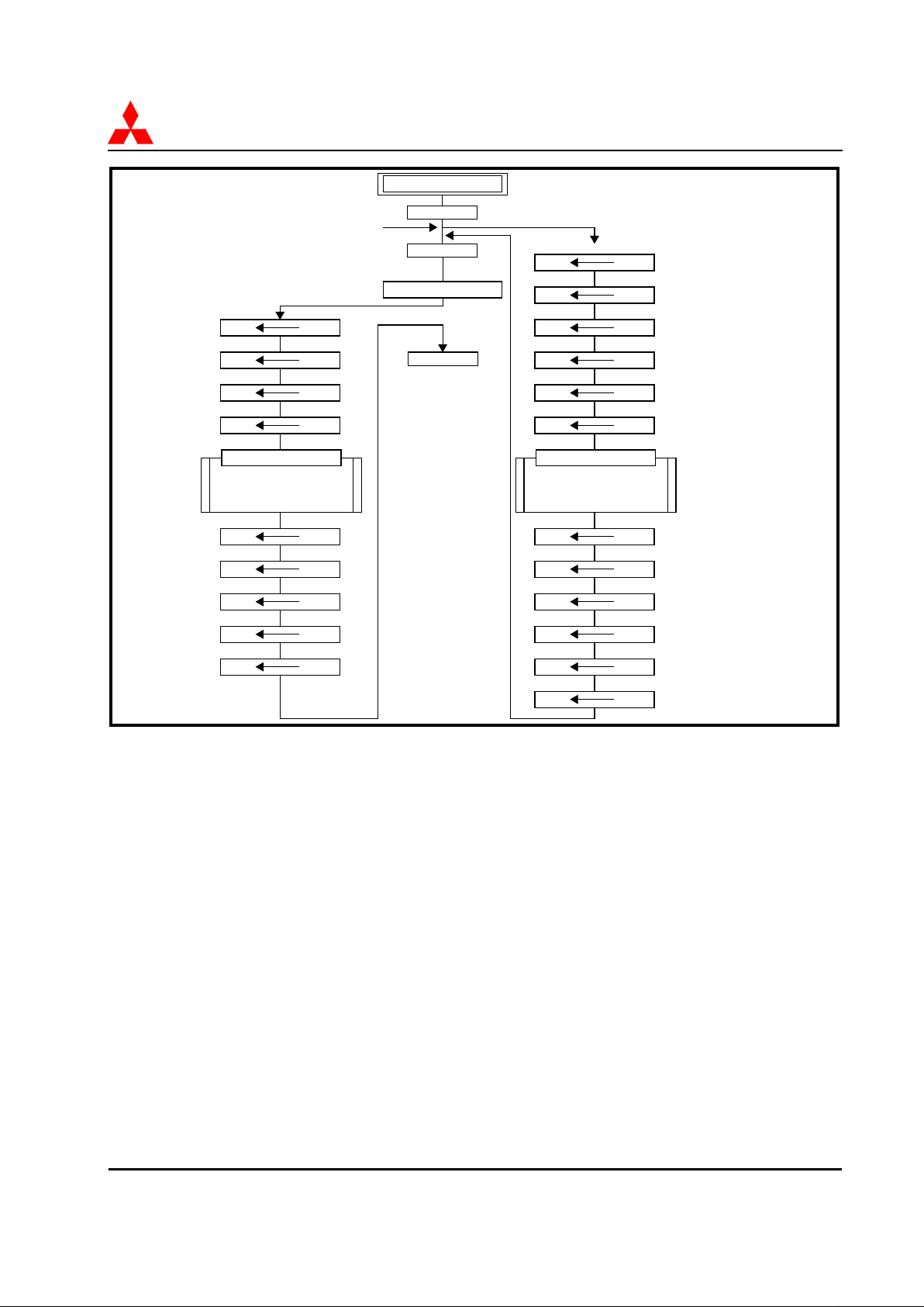
Figure 2-2. Register Push and Pop when Servicing Interrupts and Calling Subroutines
Note 1. The condition to enable an interrupt: Interrupt enable bit is set to a “1” and Interrupt inhibit
flag (I flag) is a “0”.
Note 2. When an interrupt occurs, the address of the next instruction to be executed is stored on the
stack. When a subroutine is called, the address of (next instruction -1) to be executed is stored
on the stack.
2.1.6 Processor Status Register
The processor status (PS) register is an 8-bit register consisting of flags that indicate the status of the
processor after an arithmetic operation. Branch operations can be performed by testing the Carry (C),
Zero (Z), Overflow (V), or the Negative (N) flags.
After reset, the I flag is set to a “1”, but all other flags are undefined. Because the T and D flags
directly affect arithmetic operations, they should be initialized in the beginning of a program.
Carry Flag (C)
The C flag contains a carry or borrow generated by the arithmetic logic unit (ALU) immediately
after an arithmetic operation. It is also affected by shift and rotate instructions. The C flag can be
set directly by the set carry (SEC) instruction and cleared by the clear carry (CLC) instruction.
Main Routine
. . . . . . .
. . . . . . .
Execute JSR
M(S)
(PCh)
(S)
(S-1)
M(S)
(PCl)
(S)
(S-1)
Subroutine
Execute RTS
(S)
(S+1)
(PCl) M(S)
(S)
(S+1)
(PCh)
M(S)
(PC) (PC+1)
M(S)
(PS)
(S)
(S-1)
Interrupt Routine
Execute RTI
(S)
(S+1)
(PS) M(S)
Interrupt Request
(Note 1)
Return Address Stored
on Stack (Note 2)
Return Address
Restored
Contents of
Processor Status
Register Restored on Stack
Contents of
Processor Status
Register Restored
I Flag set high
Jump Vector Fetched
Return Address Stored
on Stack (Note 2)
Return Address
Restored
M(S)
(PCh)
(S)
(S-1)
M(S)
(PCl)
(S)
(S-1)
(S)
(S+1)
(PCl) M(S)
(S)
(S+1)
(PCh)
M(S)
. . . . . . .

2-6 7/9/98 Central Processing Unit
7600 Series
M37640E8-XXXF Preliminary Specification Mitsubishi Microcomputers
Zero Flag (Z)
The Z flag is set if the result of an arithmetic operation or a data transfer is “0”, and cleared if the
result is anything other than “0”.
Interrupt Disable Flag (I)
The I flag disables all interrupts except for the interrupt generated by the BRK instruction and any
non-maskable interrupts, if available. Interrupts are disabled when the I flag is “1”. When an
interrupt occurs, this flag is automatically set to a “1” to prevent other interrupts from interfering
until the current interrupt service routine is completed. The I flag can be set by the set interrupt
disable (SEI) instruction and cleared by the clear interrupt disable (CLI) instruction.
Decimal Mode Flag (D)
The D flag determines whether additions and subtractions are executed in binary or decimal. Binary
arithmetic is executed when this flag is “0”; decimal arithmetic is executed when it is “1”. Decimal
correction is automatic in decimal mode. Only the ADC and SBC instructions can be used for
decimal arithmetic. The D flag can be set by the set decimal mode (SED) instruction and cleared by
the clear decimal mode (CLD) instruction.
Break Flag (B)
The B flag is used to indicate whether the current interrupt was generated by the BRK instruction.
The BRK flag in the processor status register is nominally “0”. When the BRK instruction is used
to generate an interrupt, the processor status register is pushed onto the stack with the break flag set
to a “1”. The saved processor status is the only place where the break flag is ever set.
Index X Mode Flag (T)
When the T flag is “0”, arithmetic operations are performed between accumulator and memory, and
the results are stored in the accumulator. When the T flag is “1”, direct arithmetic operations and
direct data transfers are enabled between memory and memory, as well as between I/O and I/O. The
result of an arithmetic operation performed on data in memory location 1 and memory location 2 is
stored in memory location 1.
The address of memory location 1 is specified by index register X, and the address of memory
location 2 is specified by normal addressing modes. The T flag can be set by the set T flag (SET)
instruction and cleared by the clear T flag (CLT) instruction. Because the T flag directly affects
calculations, it should be initialized after a reset.
Overflow Flag (V)
The V flag is used during the addition or subtraction of one byte of signed data. It is set if the
result exceeds the range from +127 to -128. When the BIT instruction is executed, bit 6 of the
memory location operated on by the BIT instruction is stored in the overflow flag. The V flag can
be cleared by the CLV instruction, but there is no set instruction. In decimal mode, the V flag is
invalid.
Negative Flag (N)
The N flag is set if the result of an arithmetic operation or data transfer is negative, that is (bit 7
is “1”). When the BIT instruction is executed, bit 7 of the memory location operated by the BIT
instruction is stored in the negative flag. There are no instructions for directly setting or clearing the
N flag.
7600 Series
Mitsubishi Microcomputer M37640E8-XXXF Preliminary Specification
CPU Mode Registers 7/9/98 2-7
2.2 CPU Mode Registers
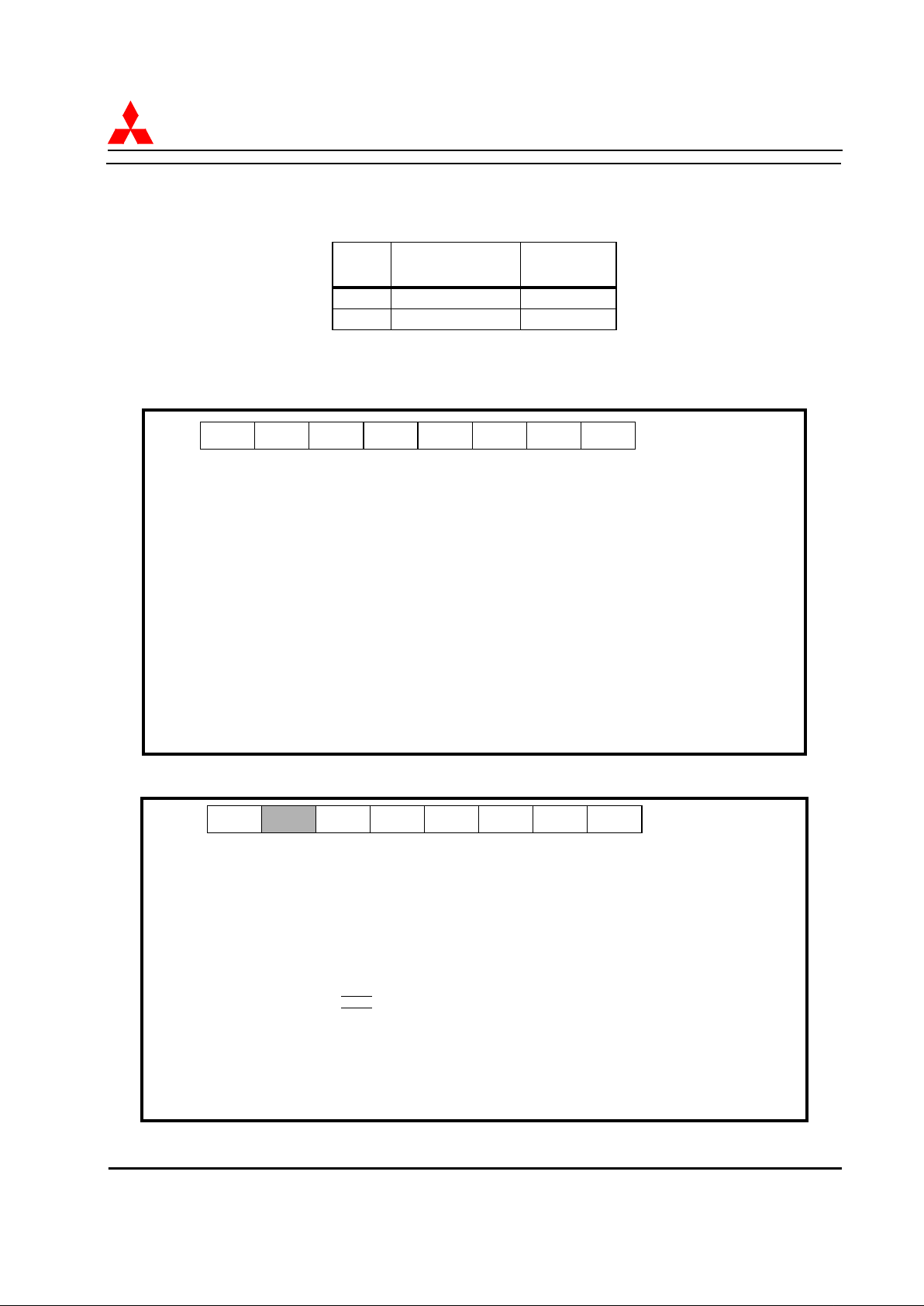
This device has two CPU mode registers: CPU Mode Register A (CPMA) and CPU Mode Register B
(CPMB) that control the processor mode, clock, slow memory wait and other CPU functions. The bit
representation of each register is described in Figure 2-3 and Figure 2-4:
Figure 2-3. CPU Mode Register A
Figure 2-4. CPU Mode Register B
Address Description
Acronym and
Value at Reset
0000
16
CPU mode register A
CPMA=0C
0001
16
CPU mode register B
CPMB=83
CPMA0,1 Processor Mode Bits (bits 1,0)
Bit 1 Bit 0
0 0: Single-Chip Mode
0 1: Memory Expansion Mode
1 0: Microprocessor Mode
1 1: Not used
CPMA2 Stack Page Selection Bit (bit 2)
0: In page 0 area
1: In page 1 area
CPMA3 X
cout
Drive Capacity Selection Bit (bit 3)
0: Low
1: High
CPMA4 Clock XC
in
-XC
out
Stop Bit (bit 4)
0: Stop
1: Oscillator
CPMA5 Clock X
in-Xout
Stop Bit (bit 5)
0: Oscillator
1: Stop
CPMA6 Internal Clock Selection Bit (bit 6)
0: External Clock
1: f
syn
CPMA7 External Clock Selection Bit (bit 7)
0: X
in-Xout
1: XCin-XC
out
MSB
7
LSB
0
CPMA7 CPMA6 CPMA5 CPMA4 CPMA3 CPMA2 CPMA1 CPMA0
Access: R/W
Reset: 0C
16
Address: 0000
16
CPMB0,1 Slow Memory Wait Bits (bits 1,0)
Bit 1 Bit 0
0 0: No wait
0 1: One time wait
1 0: Two time wait
1 1: Three time wait
CPMB2,3 Slow Memory Mode Bit (bits 3,2)
Bit 3 Bit 2
0 0: Software wait
0 1: Not used
1 0: Fixed wait by RDY pin L
1 1: Extended RDY wait
CPMB4 Expanded Data Memory Access Bit (bit 4)
0:
EDMA output disabled (64 Kbyte data access area)
1:
EDMA output enabled (greater than 64 Kbytes data access area)
CPMB5 HOLD Function Enable Bit (bit 5)
0: HOLD Function Disabled
1: HOLD Function Enabled
CPMB6 Reserved (Read/Write “0”)
CPMB7 X
out
Drive Capacity Selection Bit (bit 7)
0: Low
1: High (default state after reset and after STOP mode)
Access: R/W
Reset: 83
16
Address: 0001
16
MSB
7
LSB
0
CPMB4 CPMB3 CPMB2 CPMB1 CPMB0
CPMB7
Reserved
CPMB5
2-8 7/9/98 Oscillator Circuit
7600 Series
M37640E8-XXXF Preliminary Specification Mitsubishi Microcomputers
2.3 Oscillator Circuit
2.3.1 Description
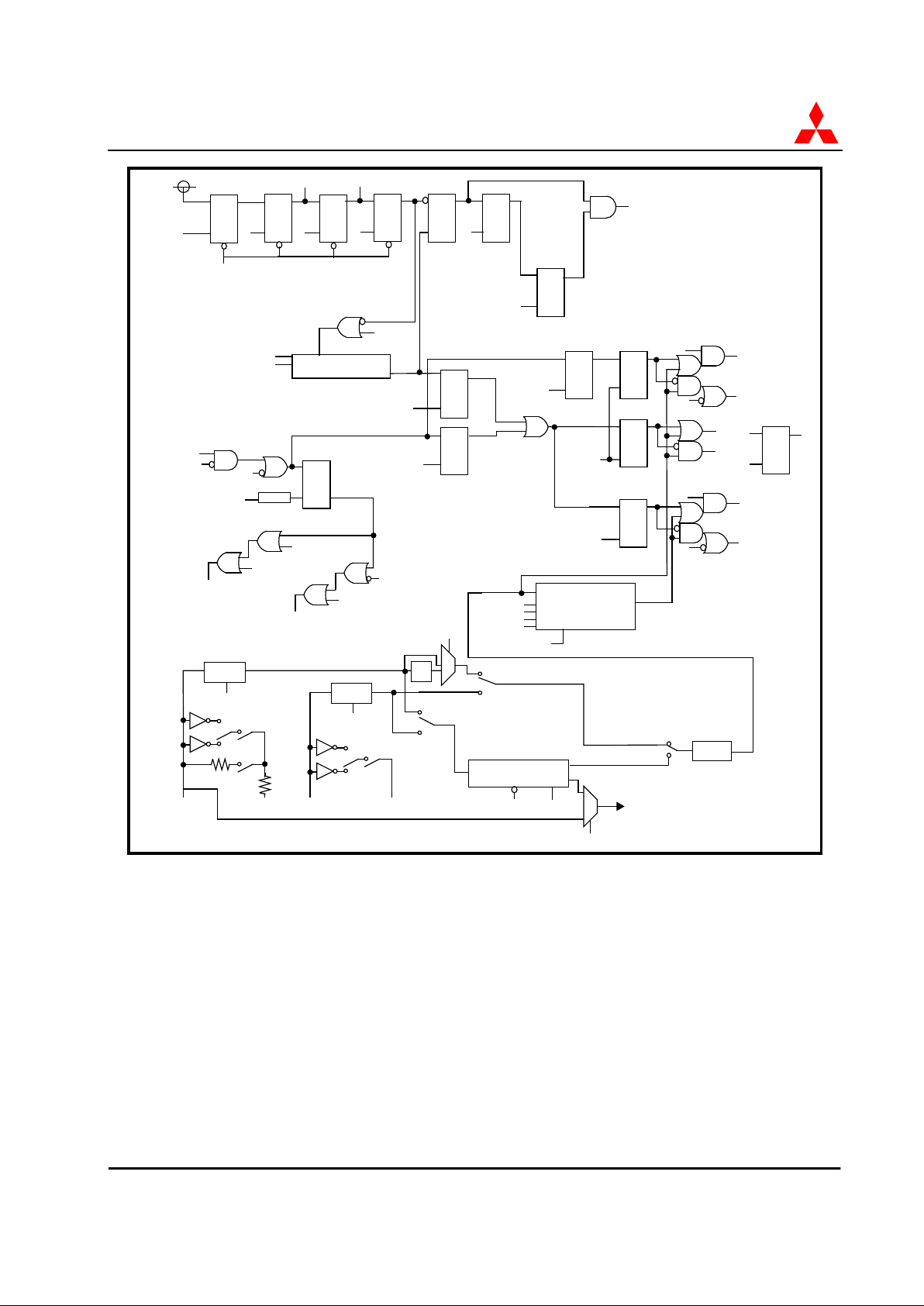
An on-chip oscillator provides the system and peripheral clocks as well as the USB clock necessary for
operation. This oscillator circuit is comprised of amplifiers that provide the gain necessary for
oscillation, oscillation control logic, a frequency synthesizer, and buffering of the clock signals. A
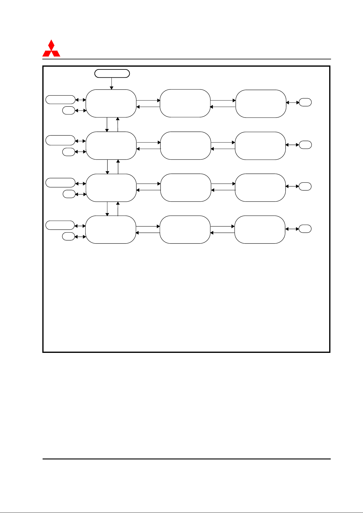
flow diagram for the oscillator circuit is shown in Figure 2-6 and a block diagram of the oscillator
circuit is shown in Figure 2-7. The following external clock inputs are supported:
• A quartz crystal oscillator of up to 24 MHz, connected to the Xin and X
out
pins.
• An external clock signal of up to 48 MHz, connected to the Xin pin.
• A ceramic resonator or quartz crystal oscillator of 32.768 kHz, connected to the XCin and XC
out
pins.
• An external clock signal of up to 5.12 MHz, connected to the XCin pin.
The frequency synthesizer can be used to generate a 48MHz clock signal (f
USB
) needed by the USB
block and clock f
SYN
, which can be chosen as the source for the system and peripheral clocks. Both
f
USB
and f
SYN
are phase-locked frequency multiples of the frequency synthesizer input. The inputs to
the frequency synthesizer can be either Xin or XCin.
The two-phase non-overlapping system clock (CPU and peripherals) is derived from the source to the
clock circuit and is 1/2 the frequency of the source. (i.e. Source = 24 MHz, system clock = 12 MHz)
Any one of four clock signals can be chosen as the source for the system and peripheral clocks; f
Xin
/
2, f
Xin
, f
XCin
, or f
SYN
. The selection is based on the values of bits CPMA6, CPMA7 and CCR7. The
default source after reset is f
Xin
/2.
The default source for the system and peripheral clocks is f
Xin
/2. If f
Xin
= 24MHz, then the CPU
will be running at Φ = 6MHz (low frequency mode. For the CPU to run in high frequency mode, i.e.,
source of clock = f
Xin
, write a “1” to bit 7 of the clock control register.
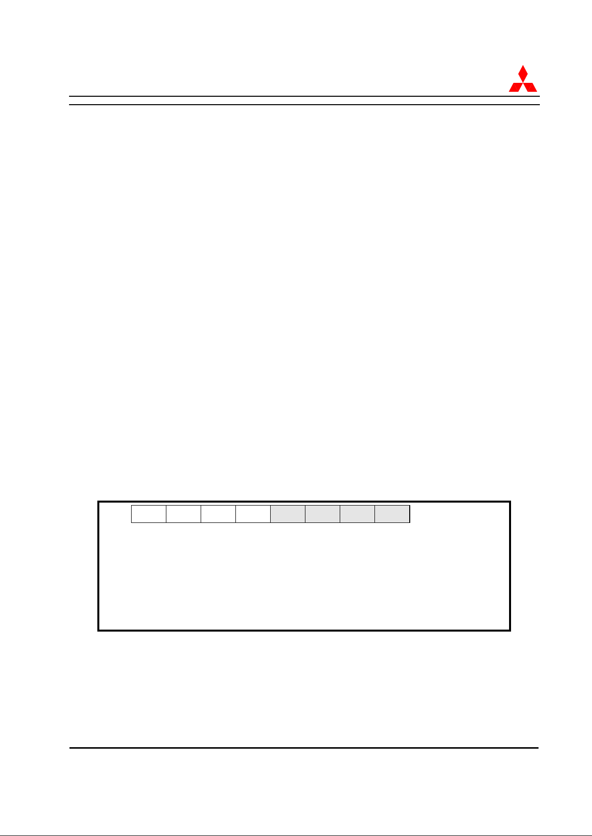
Figure 2-5. Clock Control Register
The drive strength of the X
out
and XC
out
inverting amplifier can be controlled by bits CPMB7 and
CPMA3, respectively. High drive is the default at reset or after executing a STP instruction and must
be chosen whenever restarting Xin or XCin oscillation if a ceramic or crystal oscillator is used. When
oscillation has been established, low drive can be selected to reduce power consumption. If an
external clock signal is input to Xin or XCin, the inverting amplifiers can be disabled by means of the
CCR6 and CCR7 bits, respectively, in order to reduce power consumption.
Bits 0-3 Reserved (Read/Write “0”)
CCR4: PLL Bypass Bit (bit 4)
0: f
USB
= f
VCO
(Frequency synthesizer output)
1: f
USB
= f
Xin
CCR5: XC
out
Oscillation Drive Disable Bit (bit 5)
0: XC
out
oscillation drive is enabled (when XCin oscillation is enabled).
1: XC
out
oscillation drive is disabled.
CCR6: X
out
Oscillation Drive Disable Bit (bit 6)
0: X
out
oscillation drive is enabled (when Xin oscillation is enabled).
1: X
out
oscillation drive is disabled.
CCR7: X
in
Divider Select Bit (bit 7)
0: f
Xin
/2 is used for the system clock source when CMPA7:6=00
1: f
Xin
is used for the system clock source when CMPA7:6=00
MSB
7
LSB
0
Reserved Reserved Reserved
Access: R/W
Reset: 00
16
Reserved
Address: 001F
16
CCR4
CCR7 CCR6 CCR5
7600 Series
Mitsubishi Microcomputer M37640E8-XXXF Preliminary Specification
Oscillator Circuit 7/9/98 2-9
Figure 2-6. Clock Flow Diagram
Xin clock stopped
XCin clock on
PLL clock stopped
Φ=f(XCin)/2
CPMA=BC, FSC=68
Xin clock stopped
XCin clock on
PLL clock on
Note 3
Φ=f(XCin)/2
CPMA7=BC, FSC=49
Xin clock stopped
XCin clock on
PLL clock on
Φ=f(PLL)/2
CPMA7=FC, FSC=49
Xin clock on
XCin clock on
PLL clock on
Φ=f(PLL)/2
CPMA=DC, FSC=41
Xin clock on
XCin clock on
PLL clock on
Note 3
Φ=f(XCin)/2
CPMA=9C, FSC=41
Xin clock on
XCin clock on
PLL clock stopped
Φ=f(XCin)/2
CPMA=9C, FSC=60
Xin clock on
XCin clock on
PLL clock stopped
Φ=f(Xin)/4
Note 2
CPMA=1C, FSC=60
Xin clock on
XCin clock on
PLL clock on
Note 3
Φ=f(Xin)/4
Note 2
CPMA=1C, FSC=41
Xin clock on
XCin clock on
PLL clock on
Φ=f(PLL)/2
CPMA=5C, FSC=41
Xin clock on
XCin clock stopped
PLL clock on
Φ=f(PLL)/2
CPMA=4C, FSC=41
Stop
Note 1
Wait
Stop
Note 1
Wait
Stop
Note 1
Wait
Stop
Note 1
Wait
Wait
Wait
Wait
Wait
Reset
FSC0
CPMA6
10
CPMA4
CPMA7
CPMA5
Note 4
10
10
1
0
1
0
1
0
1
0
1
0
1
0
1
0
1
0
FSC0
FSC0
FSC0
CPMA6
CPMA6
CPMA6
Note: CPMA values shown assume single-chip mode with stack in one page.
Xin clock on
XCin clock stopped
PLL clock stopped
Φ=f(Xin)/4
Note 2
CPMA=0C, FSC=60
Xin clock on
XCin clock stopped
PLL clock on
Note 3
Φ=f(Xin)/4
Note 2
CPMA=0C, FSC=41
Note 1: Stop mode stops the oscillators which are also the inputs to the frequency synthesizer.
Note 2: Φ=f(Xin)/4 can be inter-changed with Φ=f(Xin)/2 by setting CCR7 to “1”. The same
flow-chart applies for both cases.
However, the frequency synthesizer is not disabled and so its output is unstable. So, always
set the system clock to an external oscillator and disable the frequency synthesizer before
Note 3: The input to the frequency synthesizer is independent of the system clock. It can be
either Xin or XCin depending on bit 3 of FSC. In the above flow, the input has been chosen
to be the same as the system clock only for simplicity. The oscillator selected to be the input
to the frequency synthesizer must be enabled before the frequency synthesizer is enabled.
entering stop mode.
Note 4: The input clock for the frequency synthesizer must be set to XCin by setting FIN
(bit 3 of FSC) to a “1” before Xin oscillation can be disabled.
2-10 7/9/98 Oscillator Circuit
7600 Series
M37640E8-XXXF Preliminary Specification Mitsubishi Microcomputers
Figure 2-7. Clock Block Diagram
XOSCSTP
D
Q
T
R
PIN1
D
Q
T
R
R
Q
S
D
Q
T
D
Q
T
P2+
STP
Oscillator Countdown
Timer 1->2
P2 Peripheral
P1 Peripheral
PIN1
P2+
RESETB
R
Q
S
R
Q
S
D
Q
T
R
Q
S
D
Q
T
D
Q
T
S
Q
R
Φout
P2 Peripheral
P1 Peripheral
P2 Out
P1 Out
P2+
PIN2
STP
Slow Memory Wait
P1+,P2+
RDY
CPMB0
CPMB1
CPMB2
CPMB3
Frequency Synthesizer
enable
FSC0
CPMA6
PIN1,PIN2
CPMA7
f
IN
f
SYN
CPMA5
OSCSTP
DelaySTP
PadResetB
I Flag
Interrupt Request
X
in
X
out
f
Xin
XC
in
XC
out
1/2
USB 48MHz clock
CPMA3
CPMB7
CPMA4
XOSCSTP
XCOSCSTP
CPMA5
CPMA4
S
R
QB
XCOSCSTP
LPF
f
XCin
LPF
XCDOSCSTP
XCOD
XDOSCSTP
XOD
STP
WIT
D
Q
T
R
PIN1
D
Q
T
R
PIN2
PadResetB
P1HATRSTB
P2LATRSTB
P2LATRSTB
P1HATRSTB
P2
P1
P2LATRSTB
P1HATRSTB
LPF
FIN(FSC3)
f
EXT
1/2
CCR4
CCR7
7600 Series
Mitsubishi Microcomputer M37640E8-XXXF Preliminary Specification
Oscillator Circuit 7/9/98 2-11
2.3.2 Frequency Synthesizer Circuit
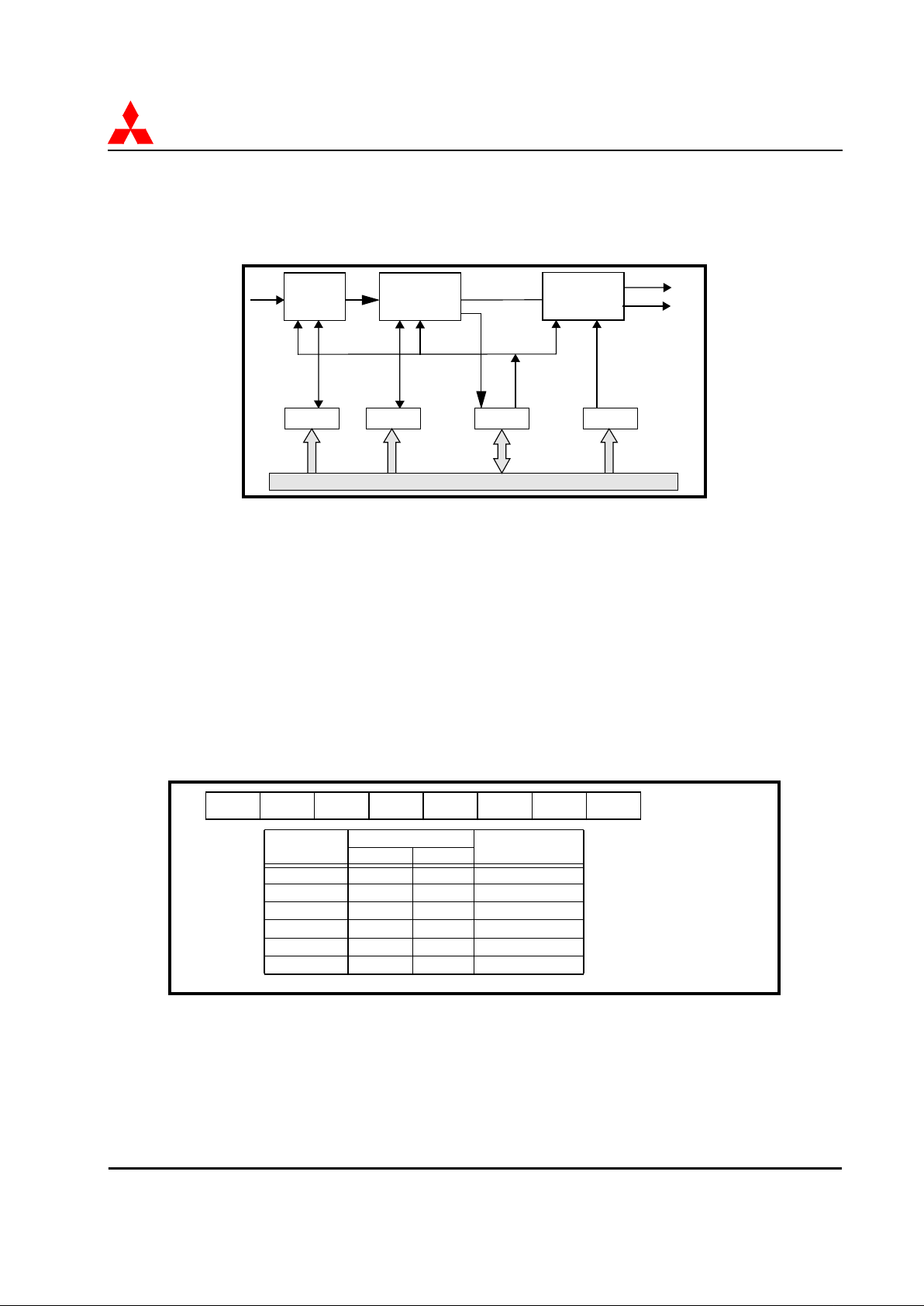
The Frequency Synthesizer Circuit generates a 48MHz clock needed by the USB block and a clock
f
SYN
that are both a multiple of the external input reference clock fIN. A block diagram of the circuit
is shown in Figure 2-8.
Figure 2-8. Frequency Synthesizer Circuit
The frequency synthesizer consists of a prescaler, frequency multiplier macro, a frequency divider
macro, and four registers, namely FSM1, FSM2, FSC and FSD. Two multiply registers (FSM1, FSM2)
control the frequency multiply amount. Clock fIN is prescaled using FSM2 to generate f
PIN
. f
PIN
is
multiplied using FSM1 to generate an f
VCO
clock which is then divided using FSD to produce the
clock f
SYN
. The f
VCO
clock is optimized for 48 MHz operation and is buffered and sent out of the
frequency synthesizer block as signal f
USB
. This signal is used by the USB block.
Clock f
PIN
is a divided down version of clock fIN, which can be either f
Xin
or f
XCin
. The default clock
after reset is f
Xin
. The relationship between f
PIN
and the clock input to the prescaler (fIN) is as
follows:
•f
PIN
= fIN / 2(n+1) where n is a decimal number between 0 and 254. Setting FSM2 to 255
disables the prescaler and f
PIN
= fIN.
Figure 2-9. Frequency Synthesizer Multiply Control Register FSM2
Data Bus
FSM2
FSM1
FSC FSD
006E
006D
006C 006F
Frequency
Multiplier
Frequency
Divider
8 Bit
LS
8 Bit
f
IN
f
VCO
f
SYN
f
USB
Prescaler
8 Bit
f
PIN
fIN/2(n+1) = f
PIN
f
PIN
FSM2
f
IN
Dec(n) Hex(n)
24 MHz 255 FF 24.00 MHz
1 MHz 11 0C 24.00 MHz
2 MHz 5 05 24.00 MHz
3 MHz 3 03 24.00 MHz
6 MHz 1 01 24.00 MHz
12 MHz 0 00 24.00 MHz
MSB
7
LSB
0
Bit 6 Bit 1 Bit 0
Bit 2
Bit 5 Bit 4 Bit 3Bit 7
Access: R/W
Address: 006E
16
Reset: FF
16
2-12 7/9/98 Oscillator Circuit
7600 Series
M37640E8-XXXF Preliminary Specification Mitsubishi Microcomputers
Figure 2-10. Frequency Synthesizer Multiply Control register FSM1
Figure 2-11. Frequency Synthesizer Divide Register
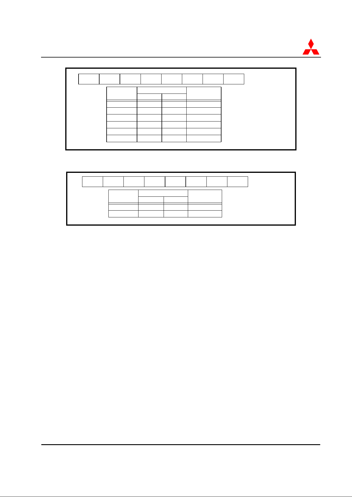
The relationship between f
PIN
, f
VCO
, and f
SYN
is as follows:
•f
VCO
= f
PIN
x 2(n+1) where n is the decimal equivalent of the value loaded in FSM2, FSM1.
Note: n must be chosen such that f
VCO
equals 48 MHz.
•f
SYN
= f
VCO
/ 2(m+1) where m is the decimal equivalent of the value loaded in FSD
Note: Setting m = 255 disables the divider and disables f
SYN
.
The FSC0 bit in the FSC Control Register enables the frequency synthesizer block. When disabled
(FSC0 = “0”), f
VCO
is held at either a high or low state. When the frequency synthesizer control bit is
active (FSC0 = “1”), a lock status (LS = “1”) indicates that f
SYN
and f
VCO
are the correct frequency.
The LS and FSCO control bits in the FSC Control register are shown in Figure 2-12.
When using the frequency synthesizer, a low-pass filter must be connected to the LPF pin.
Once the frequency synthesizer is enabled, a delay of 2-5ms is recommended before the output of the
frequency synthesizer is used. This is done to allow the output to stabilize. It is also recommended that
none of the registers be modified once the frequency synthesizer is enabled as it will cause the output
to be temporarily (2-5ms) unstable.
f
VCO
/2(n+1) = f
PIN
f
PIN
FSM1
f
VCO
Dec(n) Hex(n)
320 kHz 74 4A 48.00 MHz
2 MHz 11 0B 48.00 MHz
4 MHz 5 05 48.00 MHz
6 MHz 3 03 48.00 MHz
12 MHz 1 01 48.00 MHz
24 MHz 0 00 48.00 MHz
MSB
7
LSB
0
Bit 6 Bit 1 Bit 0
Bit 2
Bit 5 Bit 4 Bit 3Bit 7
Address: 006D
16
Access: R/W
Reset: FF
16
f
VCO
/2(m+1) = f
SYN
f
VCO
FSD
f
SYN
Dec(m) Hex(m)
48.00 MHz 00 00 24.00 MHz
48.00 MHz 127 7F 187.50 KHz
MSB
7
LSB
0
Bit 6 Bit 1 Bit 0
Address: 006F
16
Access: R/W
Reset: FF
16
Bit 2
Bit 5 Bit 4 Bit 3Bit 7

7600 Series
Mitsubishi Microcomputer M37640E8-XXXF Preliminary Specification
Oscillator Circuit 7/9/98 2-13
Figure 2-12. Frequency Synthesizer Control Register
FSE Frequency Synthesizer Enable Bit (bit 0)
0: Disabled
1: Enabled
VCO1,0 VCO Gain Control (bits 2,1)
Bit 2 Bit 1
0 0: Lowest Gain (recommended)
0 1: Low Gain
1 0: High Gain
1 1: Highest Gain
FIN Frequency Synthesizer input selector Bit (bit 3)
0: X
in
1: XC
in
Bit 4 Reserved (Read/Write “0”)
CHG1,0 LPF Current Control (bits 6,5)
Bit 6 Bit 5
0 0: Disabled
0 1: Low Current
1 0: Intermediate Current (recommended)
1 1: High Current
LS Frequency Synthesizer Lock Status Bit (bit 7) (Read Only; Write “0”)
0: Unlocked
1: Locked
MSB
7
LSB
0
CHG0 FIN VCO0 FSE
Address: 006C
16
Access: R/W
Reset: 60
16
VCO1LS
CHG1 Reserved
2-14 7/9/98 Memory Map
7600 Series
M37640E8-XXXF Preliminary Specification Mitsubishi Microcomputers
2.4 Memory Map
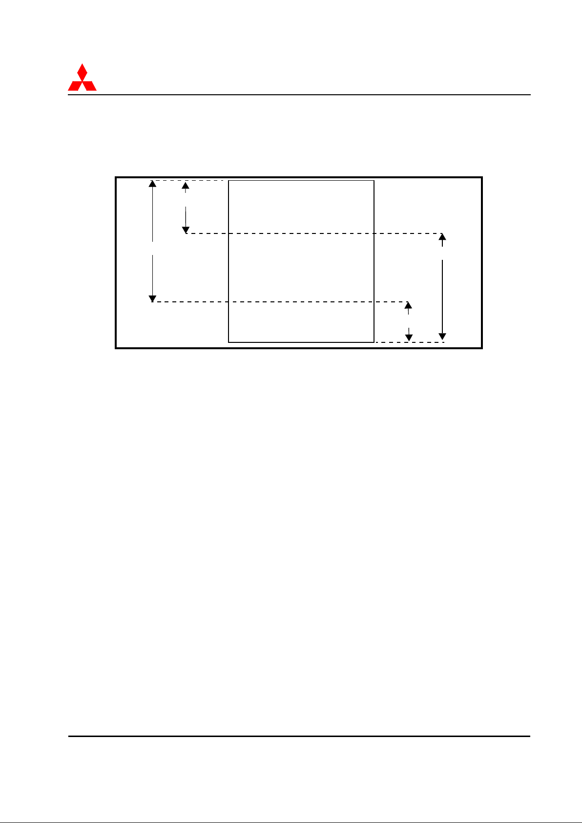
Figure 2-13. Memory Map
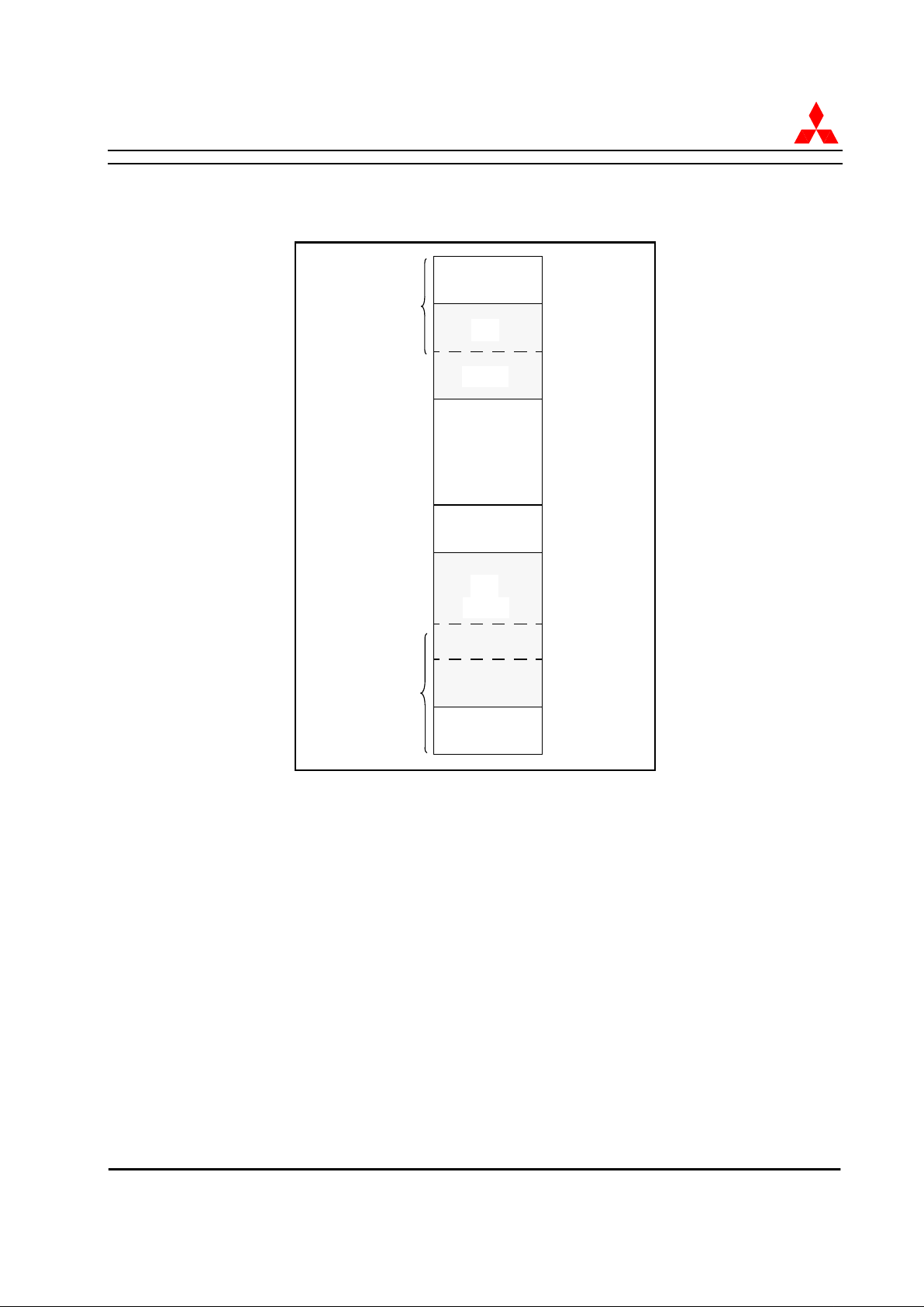
The first 112 bytes of memory from 000016 to 006F16 is the special function register (SFR) area and
contains the CPU mode registers, interrupt registers, and other registers to control peripheral functions
(see Figure 2-13.).
The general purpose RAM resides from 007016 to 046F16. When the MCU is in memory expansion
or microprocessor mode and external memory is overlaid on the internal RAM, the CPU reads data
from the internal RAM. However, the CPU writes data in both the internal and external memory. The
area from 047016 to 7FFF16 is not used in single-chip mode, but can be mapped for an external
memory device when the MCU is in memory expansion or microprocessor mode.
The area from 800016 to 807F16 and from FFFC16 to FFFF16are factory reserved areas. Mitsubishi
uses it for test and evaluation purposes. The user can not use this area in single-chip or memory
expansion modes.
The user 32K byte ROM resides from 808016 to FFFB16. When the MCU is in microprocessor mode,
the CPU accesses an external area rather than accessing the internal ROM.
Zero page and special page area can be accessed by 2-byte commands by using special addressing
modes.
SFR Area
Reserved Area
Zero Page
Special page for
subroutine calls
Not Used
Reserved Area
0000
16
006F
16
0070
16
00FF
16
0100
16
046F
16
0470
16
7FFF
16
8000
16
807F
16
8080
16
FEFF
16
FF00
16
FFC9
16
FFCA
16
FFFB
16
FFFC
16
FFFF
16
RAM
1K bytes
ROM
32K bytes
7600 Series
Mitsubishi Microcomputer M37640E8-XXXF Preliminary Specification
Memory Map 7/9/98 2-15
2.4.1 Zero page
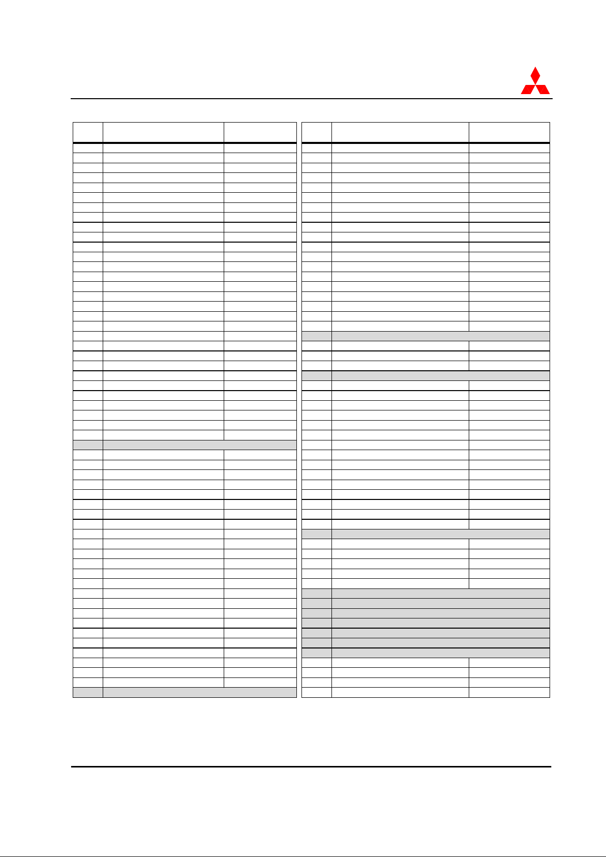
The 256 bytes zero page area is where the SFR and part of the internal RAM are allocated. The zero
page addressing modes can be used to specify memory and register addresses in this area (see
Figure 2-14.). These dedicated addressing modes enable access to this area with fewer instruction
cycles.
Figure 2-14. Zero Page and Special Page Addressing Modes
2.4.2 Special Page
The 256 bytes from address FF0016 to FFFF16 are called the special page area. In this area special
page addressing can be used to specify memory addresses (see Figure 2-14.). This dedicated special
page addressing mode enables access to this area with fewer instruction cycles. Frequently used
subroutines are normally stored in this area.
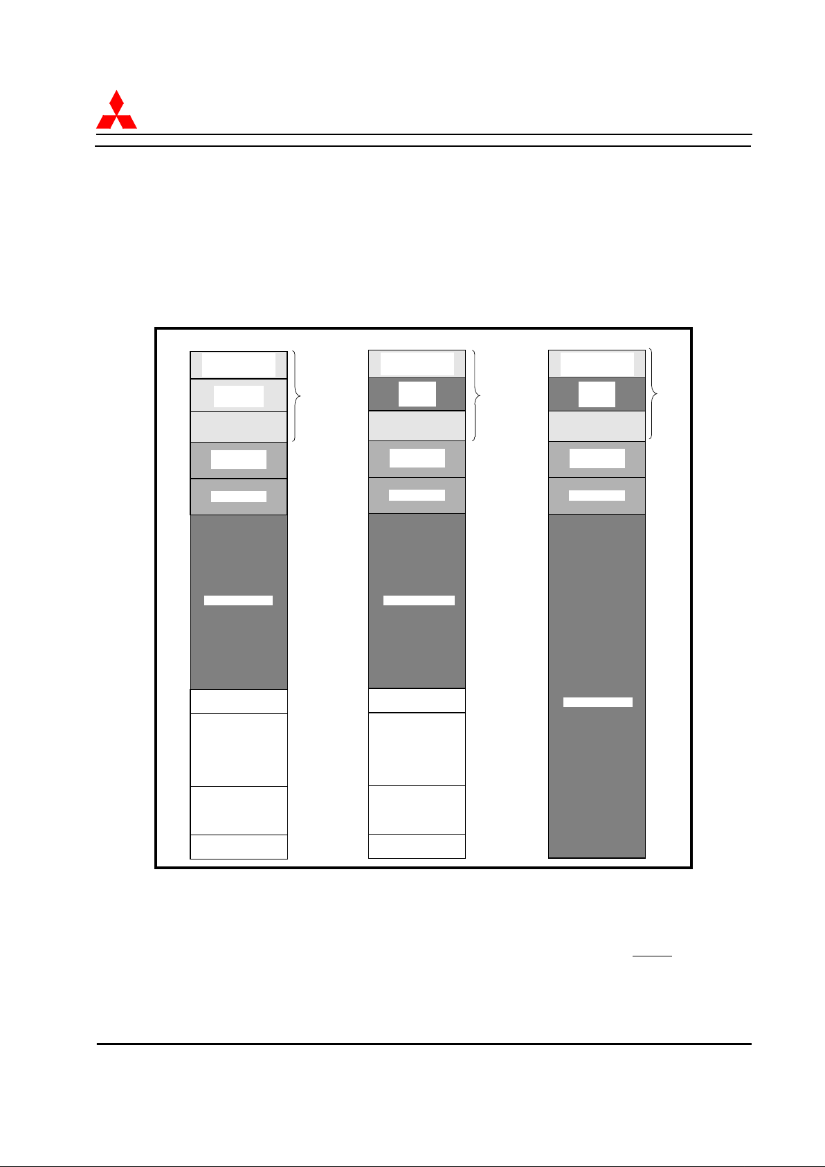
2.4.3 Special Function Registers
The special function registers (SFR) are used for controlling the functional blocks, such as I/O ports,
Timers, UART, and so forth (see Table 2-1.). The reserved addresses should not be read or written to.
Zero Page (2 byte instruction)
Zero Page Indirect (2 byte instruction)
Zero Page X (2 byte instruction)
Zero Page Y (2 byte instruction)
Zero Page Bit (2 byte instruction)
Zero Page Bit Relative (3 byte instruction)
Absolute (3 byte instruction)
Absolute X (3 byte instruction)
Absolute Y (3 byte instruction)
Relative (2 byte instruction)
Indirect (3 byte instruction)
Indirect X (2 byte instruction)
Indirect Y (2 byte instruction)
Special Page (2 byte instruction)
Addressing Modes for
zero page only
Addressing modes in which zero
page access is possible
Addressing modes in which
special page access is possible
Addressing mode
for special page
only
2-16 7/9/98 Memory Map
7600 Series
M37640E8-XXXF Preliminary Specification Mitsubishi Microcomputers
Table 2-1. SFR Addresses
Addr Description
Acronym and Value
at Reset
Addr Description
Acronym and Value at
Reset
000016CPU Mode Register A CPMA=0C 003816UART2 Mode Register U2MOD=00
000116CPU Mode Register B CPMB=03 003916UART2 Baud Rate Generator U2BRG=XX
000216Interrupt Request Register A IREQA=00 003A16UART2 Status Register U2STS=03
000316Interrupt Request Register B IREQB=00 003B16UART2 Control Register U2CON=00
000416Interrupt Request Register C IREQC=00 003C16UART2 Transmit/Receiver Buffer 1 U2TRB1=XX
000516Interrupt Control Register A ICONA=00 003D16UART2 Transmit/Receiver Buffer 2 U2TRB2=XX
000616Interrupt Control Register B ICONB=00 003E16UART2 RTS Control Register U2RTSC=80
000716Interrupt Control Register C ICONC=00 003F16DMAC Index and Status Register DMAIS=00
000816Port P0 P0=00 004016DMAC Channel x Mode Register 1 DMAxM1=00
000916Port P0 Direction Register P0D=00 004116DMAC Channel x Mode Register 2 DMAxM2=00
000A16Port P1 P1=00 004216DMAC Channel x Source Register Low DMAxSL=00
000B16Port P1 Direction Register P1D=00 004316DMAC Channel x Source Register High DMAxSH=00
000C16Port P2 P2=00 004416DMAC Channel x Destination Register Low DMAxDL=00
000D16Port P2 Direction Register P2D=00 004516DMAC Channel x Destination Register High DMAxDH=00
000E16Port P3 P3=00 004616DMAC Channel x Count Register Low DMAxCL=00
000F16Port P3 Direction Register P3D=00 004716DMAC Channel x Count Register High DMAxCH=00
001016Port Control Register PTC=00 004816Data Bus Buffer register 0 DBB0=00
001116Interrupt Polarity Selection Register IPOL=00 004916Data Bus Buffer status register 0 DBBS0=00
001216Port P2 pull-up Control Register PUP2=00 004A16Data Bus Buffer Control Register 0 DBBC0=00
001316USB Control Register USBC=00 004B16Reserved
001416Port P6 P6=00 004C16Data Bus Buffer register 1 DBB1=00
001516Port P6 Direction Register P6D=00 004D16Data Bus Buffer Status Register 1 DBBS1=00
001616Port P5 P5=00 004E16Data Bus Buffer Control Register 1 DBBC1=00
001716Port P5 Direction Register P5D=00 004F16Reserved
001816Port P4 P4=00 005016USB Address Register USBA=00
001916Port P4 Direction Register P4D=00 005116USB Power Management Register USBPM=00
001A16Port P7 P7=00 005216USB Interrupt Status Register 1 USBIS1=00
001B16Port P7 Direction Register P7D=00 005316USB Interrupt Status Register 2 USBIS2=00
001C16Port P8 P8=00 005416USB Interrupt Enable Register 1 USBIE1=00
001D16Port P8 Direction Register P8D=00 005516USB Interrupt Enable Register 2 USBIE2=00
001E16Reserved 005616USB Frame Number Register Low USBSOFL=00
001F16Clock Control Register CCR=00 005716USB Frame Number Register High USBSOFH=00
002016Timer XL TXL=FF 005816USB Endpoint Index USBINDEX=00
002116Timer XH TXH=FF 005916USB Endpoint x IN CSR IN_CSR=00
002216Timer YL TYL=FF 005A16USB Endpoint x OUT CSR OUT_CSR=00
002316Timer YH TYH=FF 005B16USB Endpoint x IN MAXP IN_MAXP=00
002416Timer 1 T1=FF 005C16USB Endpoint x OUT MAXP OUT_MAXP=00
002516Timer 2 T2=01 005D16USB Endpoint x OUT WRT_CNT Low WRT_CNTL=00
002616Timer 3 T3=FF 005E16USB Endpoint x OUT WRT_CNT High WRT_CNTH=00
002716Timer X Mode Register TXM=00 005F16Reserved
002816Timer Y Mode Register TYM=00 006016USB Endpoint 0 FIFO USBFIFO0=N/A
002916Timer 123 Mode Register T123M=00 006116USB Endpoint 1 FIFO USBFIFO1=N/A
002A16SIO Shift Register SIOSHT=XX 006216USB Endpoint 2 FIFO USBFIFO2=N/A
002B16SIO Control Register 1 SIOCON1=00 006316USB Endpoint 3 FIFO USBFIFO3=N/A
002C16SIO Control Register 2 SIOCON2=18 006416USB Endpoint 4 FIFO USBFIFO4=N/A
002D16Special Count Source Generator1 SCSG1=FF 006516Reserved
002E16Special Count Source Generator2 SCSG2=FF 006616Reserved
002F16Special Count Source Mode Register SCSM=00 006716Reserved
003016UART1 Mode Register U1MOD=00 006816Reserved
003116UART1 Baud Rate Generator U1BRG=XX 006916Reserved
003216UART1 Status Register U1STS=03 006A16Reserved
003316UART1 Control Register U1CON=00 006B16Reserved
003416UART1 Transmit/Receiver Buffer 1 U1TRB1=XX 006C16Freq Synthesizer Control FSC=60
003516UART1 Transmit/Receiver Buffer 2 U1TRB2=XX 006D16Freq Synthesizer Multiply Register 1 FSM1=FF
003616UART1 RTS Control Register U1RTSC=80 006E16Freq Synthesizer Multiply Register 2 FSM2=FF
003716Reserved 006F16Freq Synthesizer Divide Register FSD=FF
7600 Series
Mitsubishi Microcomputer M37640E8-XXXF Preliminary Specification
Processor Modes 7/9/98 2-17
2.5 Processor Modes
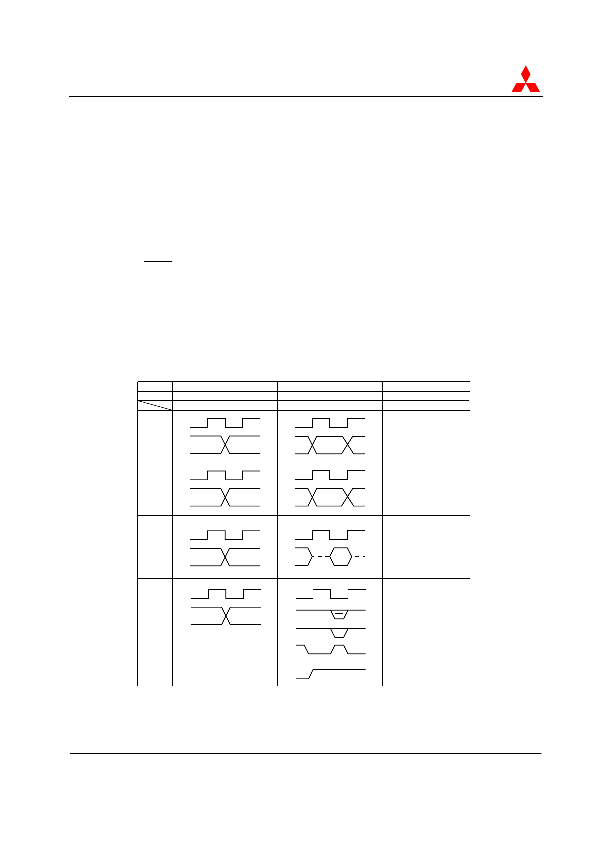
The operation modes are described below. The memory maps for the first three modes are shown in
Figure 2-15.
Single chip mode is normally entered after reset. However, if the MCU has a CNVss pin, holding this
pin high will cause microprocessor mode to be entered after reset. After the reset sequence has
completed, the mode can be changed with software by modifying the value of bits 0 and 1 of CPMA.
However, while CNVss is high, bit 1 of CPMA is “1” and cannot be changed.
Figure 2-15. Operation Modes Memory Maps
2.5.1 Single Chip
In this mode, all ports take on their primary function and all internal memory is accessible. Those
areas that are not in internal memory are not accessible. Also, slow memory wait and EDMA are
disabled in this mode.
0000
0007
0008
000F
0010
006F
0070
00FF
0100
046F
0470
7FFF
8000
807F
8080
FFC9
FFCA
FFFB
FFFC
FFFF
P0-P3
Reserved Area
Inaccessible Area
Internal RAM
(Zero Page)
Internal RAM
ROM
Interrupt
Vectors
Reserved Area
0000
0007
0008
000F
0010
006F
0070
00FF
0100
046F
0470
7FFF
8000
807F
8080
FFC9
FFCA
FFFB
FFFC
FFFF
External
Memory
Reserved Area
Internal RAM
(Zero Page)
Internal RAM
External Memory
ROM
Interrupt
Vectors
Reserved Area
0000
0007
0008
000F
0010
006F
0070
00FF
0100
046F
0470
FFFF
External
Memory
Internal RAM
(Zero Page)
Internal RAM
External Memory
SFR
SFR
SFR
Single Chip Mode Memory Expansion Mode Microprocessor Mode
CPMA, CPMB,&
Int Registers
CPMA, CPMB,&
Int Registers
CPMA, CPMB,&
Int Registers
2-18 7/9/98 Processor Modes
7600 Series
M37640E8-XXXF Preliminary Specification Mitsubishi Microcomputers
2.5.2 Memory Expansion
In this mode, Ports 0 and 1 output the address bus (AB0-AB15), port 2 acts as the data bus input and
output, and port 3 bits 7 to 3 output RD, WR, SYNCout, Φout, and DMAout, respectively. All
memory areas that are not internal memory or SFR area are accessed externally. Because ports 0 to 3
lose their normal function in this mode, the address area for the ports and their direction registers are
treated as external memory (see Figure 2-15.) In this mode, slow memory wait and EDMA can be
enabled.
2.5.3 Microprocessor
This mode is primarily the same as memory expansion mode. The difference is that the internal
ROM / EPROM area can not be accessed and is instead treated as external memory. Slow memory
wait and EDMA can be enabled in this mode.
2.5.4 EPROM
This mode is used for programming and testing the internal EPROM. In this mode, ports 0 and 1
input the address, port 2 acts as the data bus input and output, and port 3 bits 7, 6, 3 and 2 input
OEB, CEB, PGMB, and VRFY, respectively.
Figure 2-16. Function of Ports P0-P3 in each Processor Mode
CPMA1
CPMA0
Port P0
0
0011
0
Port P1
Port P2
Port P3
Mode
Port
Single Chip Mode
Microprocessor Mode
Memory Expansion
Mode
Φ
Internal
Φ
Internal
Port P0
7
- P0
0
I/O Port
Port P07 - P0
0
Address
Output
AB7 - AB
0
Same as
Microprocessor Mode
Internal
Port P1
7
- P1
0
I/O Port
Internal
Port P2
7
- P1
0
I/O Port
Φ
Internal
Port P17 - P1
0
Address
Output
AB15 - AB
8
Same as
Microprocessor Mode
Φ
Internal
Port P3
7
- P3
0
I/O Port
Φ
Internal
Port P27 - P2
0
Data
I/O
DB7 - DB
0
Φ
Internal
Same as
Microprocessor Mode
Same as
Microprocessor Mode
Port 3
4
Port 3
7
Port 3
6
Port 3
5
Port 3
3
RD
Output
WR Output
SYNCout
DMAout Output
Φ
Φ
 Loading...