

Datasheet M30624MGA-XXXGP, M30624MGA-XXXFP, M30624FGAGP, M30624FGAFP, M30622M8A-XXXFP Datasheet (Mitsubishi)
...
Mitsubishi microcomputers
M16C / 62A Group
SINGLE-CHIP 16-BIT CMOS MICROCOMPUTER
Description
Description
The M16C/62A group of single-chip microcomputers are built using the high-performance silicon gate
CMOS process using a M16C/60 Series CPU core and are packaged in a 100-pin plastic molded QFP.
These single-chip microcomputers operate using sophisticated instructions featuring a high level of instruction efficiency. With 1M bytes of address space, they are capable of executing instructions at high speed.
They also feature a built-in multiplier and DMAC, making them ideal for controlling office, communications,
industrial equipment, and other high-speed processing applications.
The M16C/62A group includes a wide range of products with different internal memory types and sizes and
various package types.
Features
• Memory capacity..................................ROM (See Figure 1.1.4. ROM Expansion)
RAM 3K to 20K bytes
• Shortest instruction execution time......62.5ns (f(XIN)=16MHZ, VCC=5V)
100ns (f(XIN)=10MHZ, VCC=3V, with software one-wait) : Mask ROM, flash memory 5V version
• Supply voltage .....................................
• Low power consumption ......................25.5mW ( f(XIN)=10MHZ, with software one-wait, VCC = 3V)
• Interrupts..............................................25 internal and 8 external interrupt sources, 4 software
• Multifunction 16-bit timer......................5 output timers + 6 input timers
• Serial I/O..............................................5 channels
• DMAC ..................................................2 channels (trigger: 24 sources)
• A-D converter.......................................10 bits X 8 channels (Expandable up to 10 channels)
• D-A converter.......................................8 bits X 2 channels
• CRC calculation circuit.........................1 circuit
• Watchdog timer....................................1 line
• Programmable I/O ...............................87 lines
• Input port..............................................
• Memory expansion ..............................Available (to a maximum of 1M bytes)
• Chip select output ................................4 lines
• Clock generating circuit .......................2 built-in clock generation circuits
4.2V to 5.5V (f(XIN)=16MHZ, without software wait) : Mask ROM, flash memory
2.7V to 5.5V (f(XIN)=10MHZ with software one-wait) :
interrupt sources; 7 levels (including key input interrupt)
(3 for UART or clock synchronous, 2 for clock synchro-
nous)
_______
1 line (P85 shared with NMI pin)
(built-in feedback resistor, and external ceramic or quartz oscillator)
Mask ROM, flash memory 5V version
5V
version
Applications
Audio, cameras, office equipment, communications equipment, portable equipment
Central Processing Unit (CPU) .....................11
Reset.............................................................14
Processor Mode............................................ 21
Clock Generating Circuit ............................... 34
Protection......................................................43
Interrupts.......................................................44
Watchdog Timer............................................64
DMAC ...........................................................66
------Table of Contents------
Timer.............................................................76
Serial I/O .....................................................106
A-D Converter ............................................. 147
D-A Converter ............................................. 157
CRC Calculation Circuit ..............................159
Programmable I/O Ports .............................161
Electrical characteristic ...............................176
Flash memory version.................................227
1
s
p
R
Description
Pin Configuration
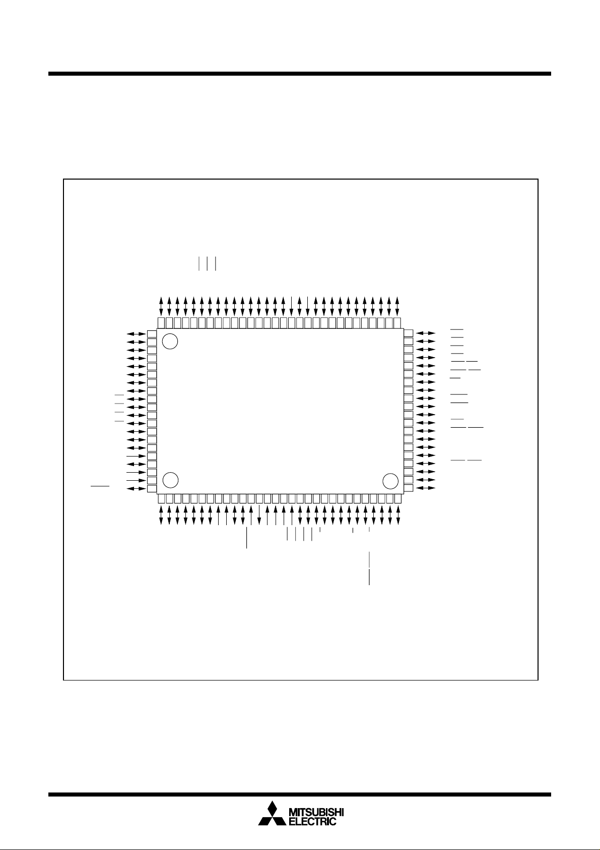
Figures 1.1.1 and 1.1.2 show the pin configurations (top view).
PIN CONFIGURATION (top view)
)
)
)
3
/D
4
(/D
4
/A
4
P2
4
/D
5
(/D
5
/A
5
P2
5
/D
6
(/D
6
/A
6
P2
)
6
/D
7
(/D
7
/A
7
P2
Vss
)
)
)
0
1
2
/D
/D
/D
/-)
1
2
3
0
/INT5
/INT4
/INT3
10
8
11
12
9
/D
/D
0
1
P1
P1
13
/D
/D
/D
/D
2
3
4
5
P1
P1
P1
P1
(/D
(/D
(/D
(/D
15
14
1
2
3
0
/D
/D
/A
/A
/A
/A
7
6
1
2
3
0
P1
P1
P2
P2
P2
P2
)
7
(/-/D
8
/A
0
P3
Vcc
Mitsubishi microcomputer
M16C / 62A Grou
SINGLE-CHIP 16-BIT CMOS MICROCOMPUTE
9
10
11
/A
/A
/A
1
2
3
P3
P3
P3
15
16
17
12
13
14
/A
/A
/A
4
5
6
P3
P3
P3
18
/A
7
P3
19
/A
/A
/A
/A
0
1
2
3
P4
P4
P4
P4
P107/AN7/KI
P106/AN6/KI
P105/AN5/KI
P104/AN4/KI
P103/AN
P102/AN
P101/AN
P100/AN
P97/AD
P07/D
P06/D
P05/D
P04/D
P03/D
P02/D
P01/D
P00/D
AV
V
AVcc
TRG/SIN
REF
/W
OUT
/TA2
4
P7
/V
IN
/TA1
2
/RTS
2
/CTS
3
P7
515253545556575859606162636465666768697071727374757677787980
IN
/V
OUT
/TB5
IN
/TA1
2
/CLK
2
/SCL/TA0
2
P7
/RxD
1
P7
50
49
48
47
46
45
44
43
42
41
40
39
38
37
36
35
34
33
32
31
OUT
/SDA/TA0
2
D
X
/T
0
P7
7
81
6
82
5
83
4
84
3
85
2
86
1
87
0
88
3
89
2
90
1
91
92
0
93
3
94
2
95
1
SS
96
97
0
98
99
00
1
4
1 2 3 4 5 6 7 8 9 101112131415161718192021222324252627282930
4
OUT
/ANEX0/CLK4
/ANEX1/S
5
6
P9
P9
M16C/62A Group
3
IN
/TB4
1
/DA
4
P9
IN
/TB3
0
/DA
3
P9
3
OUT
/S
IN
/TB2
2
P9
IN
/S
IN
/TB1
1
P9
BYTE
/CLK3
IN
/TB0
0
P9
CIN
/X
7
CNVss
P8
COUT
/X
6
P8
OUT
X
RESET
IN
SS
CC
X
V
V
/NMI
5
P8
2
/INT
4
P8
1
/INT
3
P8
0
/INT
2
P8
/U
IN
/TA4
1
P8
/U
OUT
/TA4
0
P8
IN
/TA3
7
P7
OUT
/TA3
6
P7
/W
IN
/TA2
5
P7
P44/CS0
P45/CS1
P46/CS2
P47/CS3
P50/WRL/WR
P51/WRH/BHE
P5
2
/RD
P53/BCLK
P54/HLDA
P55/HOLD
P56/ALE
P57/RDY/CLK
P60/CTS0/RTS
P61/CLK
P62/RxD
P6
3/TXD0
P64/CTS1/RTS1/CLKS
P65/CLK
P66/RxD
P67/TXD
OUT
0
0
0
1
1
1
1
Figure 1.1.1. Pin configuration (top view)
2
Package: 100P6S-A
Mitsubishi microcomputers
M16C / 62A Group
SINGLE-CHIP 16-BIT CMOS MICROCOMPUTER
Description
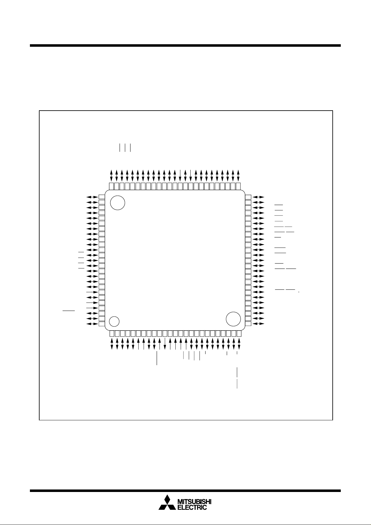
PIN CONFIGURATION (top view)
P12/D
P11/D
P10/D
P07/D
P06/D
P05/D
P04/D
P03/D
P02/D
P01/D
P00/D
P107/AN7/KI
P106/AN6/KI
P105/AN5/KI
P104/AN4/KI
P103/AN
P102/AN
P101/AN
AV
P100/AN
V
P9
P97/AD
6
TRG/SIN
/ANEX1/S
AVcc
OUT
P95/ANEX0/CLK4
REF
)
3
/D
4
(/D
4
/A
4
P2
)
4
/D
5
(/D
5
/A
5
P2
)
5
/D
6
(/D
6
/A
6
P2
)
6
/D
7
(/D
7
/A
7
P2
Vss
)
7
(/-/D
8
/A
0
P3
Vcc
9
/A
1
P3
10
/A
2
P3
11
/A
3
P3
12
/A
4
P3
13
/A
5
P3
14
/A
6
P3
15
/A
7
P3
16
17
/A
/A
0
1
P4
P4
525354555657585960616263646566676869707172737475
51
P42/A
50
49
48
47
46
45
44
43
42
41
40
39
38
37
36
35
34
33
32
31
30
29
28
27
26
18
P43/A
19
P44/CS0
P45/CS1
P46/CS2
P47/CS3
P50/WRL/WR
P51/WRH/BHE
2
/RD
P5
P53/BCLK
P54/HLDA
P55/HOLD
P56/ALE
P57/RDY/CLK
P60/CTS0/RTS
P61/CLK
P62/RxD
3/TXD0
P6
OUT
0
0
0
P64/CTS1/RTS1/CLKS
P65/CLK
1
P66/RxD
1
P67/TXD
1
P70/TXD2/SDA/TA0
1
/RxD2/SCL/TA0IN/TB5
P7
P72/CLK2/TA1
OUT
/V
OUT
1
IN
)
)
)
1
0
/-)
0
(/D
0
/A
0
P2
/D
1
(/D
1
/A
1
P2
/D
2
(/D
2
/A
2
P2
2
/D
3
(/D
3
/A
3
P2
3
4
5
/INT
/INT
11
/D
3
P1
10
SS
76
9
77
8
78
7
79
6
80
5
81
4
82
3
83
2
84
1
85
0
86
3
87
2
88
1
89
0
90
3
91
2
92
1
93
94
95
0
96
97
4
98
4
99
00
1
1 2 3 4 5 6 7 8 9 10111213141516171819202122 23 24 25
/INT
12
13
14
15
/D
/D
/D
/D
4
5
6
7
P1
P1
P1
P1
M16C/62A Group
Figure 1.1.2. Pin configuration (top view)
IN
/TB4
1
/DA
4
P9
IN
/TB3
0
/DA
3
P9
3
OUT
/S
IN
/TB2
2
P9
3
IN
/S
IN
/TB1
1
P9
BYTE
/CLK3
IN
/TB0
0
P9
CIN
/X
7
CNVss
P8
COUT
/X
6
P8
OUT
X
RESET
1
2
/NMI
5
P8
/INT
4
P8
/INT
3
P8
0
/INT
2
P8
/U
IN
/TA4
1
P8
/U
OUT
/TA4
0
P8
IN
/TA3
7
P7
OUT
/TA3
6
P7
/W
IN
/TA2
5
P7
/W
OUT
/TA2
4
P7
/V
IN
/TA1
2
/RTS
2
/CTS
3
Package: 100P6Q-A
P7
IN
SS
CC
X
V
V
3
s
p
R
Description
A
A
A
ote
depends o
type
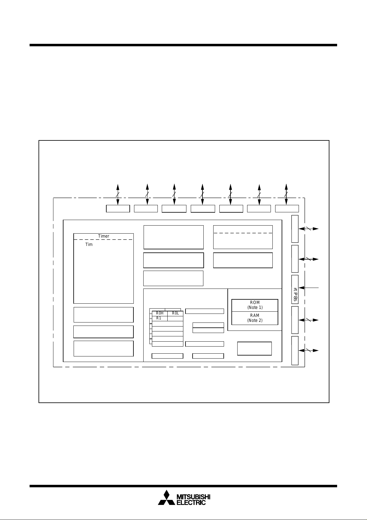
Block Diagram
Figure 1.1.3 is a block diagram of the M16C/62A group.
Block diagram of the M16C/62A group
Mitsubishi microcomputer
M16C / 62A Grou
SINGLE-CHIP 16-BIT CMOS MICROCOMPUTE
8
I/O ports
Internal peripheral functions
Timer TA0 (16 bits)
Timer TA1 (16 bits)
Timer TA2 (16 bits)
Timer TA3 (16 bits)
Timer TA4 (16 bits)
Timer TB0 (16 bits)
Timer TB1 (16 bits)
Timer TB2 (16 bits)
Timer TB3 (16 bits)
Timer TB4 (16 bits)
Timer TB5 (16 bits)
Port P08Port P18Port P28Port P38Port P48Port P58Port P6
Timer
Expandable up to 10 channels)
UART/clock synchronous SI/O
CRC arithmetic circuit (CCITT )
(Polynomial : X
M16C/60 series16-bit CPU core
Watchdog timer
(15 bits)
DMAC
(2 channels)
D-A converter
(8 bits X 2 channels)
Note 1: ROM size depends on MCU type.
N
2: RAM size
n MCU
A-D converter
(10 bits X 8 channels
(8 bits X 3 channels)
16+X12+X5
Registers
R0LR0H
R1H R1L
R0LR0H
R1H R1L
R2
R2
R3
R3
A0
A0
A1
A1
FB
FB
SB FLG
.
+1)
Program counter
PC
Stack pointer
ISP
USP
Vector table
INTB
Flag register
System clock generator
X
IN-XOUT
X
CIN-XCOUT
Clock synchronous SI/O
(8 bits X 2 channels)
Memory
ROM
AAAA
(Note 1)
RAM
AAAA
(Note 2)
AAAA
Multiplier
Port P7
8
Port P8
7
Port P8
5
Port P9
8
Port P10
8
Figure 1.1.3. Block diagram of M16C/62A group
4
Mitsubishi microcomputers
M16C / 62A Group
SINGLE-CHIP 16-BIT CMOS MICROCOMPUTER
Description
Performance Outline
Table 1.1.1 is a performance outline of M16C/62A group.
Table 1.1.1. Performance outline of M16C/62A group
Item Performance
Number of basic instructions 91 instructions
Shortest instruction execution time 62.5ns(f(XIN)=16MHZ,
100ns (f(XIN)=10MHZ, VCC=3V, with software one-wait)
: Mask ROM, flash memory 5V version
Memory ROM (See the figure 1.1.4. ROM Expansion)
capacity RAM 3K to 20K bytes
I/O port P0 to P10 (except P85) 8 bits x 10, 7 bits x 1
Input port P85 1 bit x 1
Multifunction TA0, TA1, TA2, TA3, TA4 16 bits x 5
timer TB0, TB1, TB2, TB3, TB4, TB5 16 bits x 6
Serial I/O UART0, UART1, UART2 (UART or clock synchronous) x 3
SI/O3, SI/O4 (Clock synchronous) x 2
A-D converter 10 bits x (8 + 2) channels
D-A converter 8 bits x 2
DMAC 2 channels (trigger: 24 sources)
CRC calculation circuit CRC-CCITT
Watchdog timer 15 bits x 1 (with prescaler)
Interrupt
Clock generating circuit 2 built-in clock generation circuits
Supply voltage 4.2V to 5.5V (f(XIN)=16MHZ, without software wait)
Power consumption
I/O I/O withstand voltage 5V
characteristics
Memory expansion Available (to a maximum of 1M bytes)
Device configuration CMOS high performance silicon gate
Package 100-pin plastic mold QFP
Output current 5mA
25 internal and 8 external sources, 4 software sources, 7 levels
(built-in feedback resistor, and external ceramic or quartz oscillator)
: Mask ROM, flash memory 5V version
2.7V to 5.5V (f(XIN)=10MHZ with software one-wait)
: Mask ROM, flash memory 5V version
25.5mW (f(XIN) = 10MHZ, VCC=3V with software one-wait)
VCC=5V
)
5
s
p
R
Description
p
SINGLE-CHIP 16-BIT CMOS MICROCOMPUTE
Mitsubishi plans to release the following products in the M16C/62A group:
(1) Support for mask ROM version, external ROM version, and flash memory version
(2) ROM capacity
(3) Package
100P6S-A : Plastic molded QFP (mask ROM, one-time PROM, and flash memory versions)
100P6Q-A : Plastic molded QFP(mask ROM, one-time PROM, and flash memory versions)
ROM Size
(Byte)
External
ROM
256K
128K
96K
64K
32K
M30624MGA-XXXFP/GP
M30620MCA-XXXFP/GP
M30622MCA-XXXFP/GP
M30620MAA-XXXFP/GP
M30622MAA-XXXFP/GP
M30620M8A-XXXFP/GP
M30622M8A-XXXFP/GP
M30622M4A-XXXFP/GP
Mask ROM version
M30624FGAFP/GP
M30620FCAFP/GP
Flash memory version
M30620SAFP/GP
M30622SAFP/GP
External ROM version
Mitsubishi microcomputer
M16C / 62A Grou
Figure 1.1.4. ROM expansion
The M16C/62A group products currently supported are listed in Table 1.1.2.
Table 1.1.2. M16C/62A group
ROM capacity
M30622M4A-XXXFP
M30622M4A-XXXGP 100P6Q-A
M30620M8A-XXXFP
M30620M8A-XXXGP 100P6Q-A
M30622M8A-XXXFP
M30622M8A-XXXGP
M30620MAA-XXXFP
M30620MAA-XXXGP
M30622MAA-XXXFP
M30622MAA-XXXGP 100P6Q-A
M30620MCA-XXXFP
M30620MCA-XXXGP
M30622MCA-XXXFP
M30622MCA-XXXGP
M30624MGA-XXXFP
M30624MGA-XXXGP 100P6Q-A
M30620FCAFP
M30620FCAGP
M30624FGAFP
M30624FGAGP
**
**
**
**
**
**
**
**
**
**
**
**
**
**
**
**
**
**
**
**
32K byte
64K byte
96K byte
128K byte
256K byte
128K byte
256K byte
**
M30620SAGP
M30622SAFP
M30622SAGP
**: Under develo
ment
**
**
**
RAM capacity
3K byte
10K byte
4K byte
10K byte
5K byte
10K byte
5K byte
20K byte
10K byte
20K byte
10K byte
3K byte
Package type
100P6S-A
100P6S-A
100P6S-A
100P6Q-A
100P6S-A
100P6Q-A
100P6S-A
100P6S-A
100P6Q-A
100P6S-A
100P6Q-A
100P6S-A
100P6S-A
100P6Q-A
100P6S-A
100P6Q-A
100P6S-AM30620SAFP
100P6Q-A
100P6S-A
100P6QA-A
December. 1999
RemarksType No
Mask ROM version
Flash memory
5V version
External ROM
version
6

Mitsubishi microcomputers
M16C / 62A Group
SINGLE-CHIP 16-BIT CMOS MICROCOMPUTER
Description
Type No. M 3 0 6 2 2 M 8 A– X X X F P
Package type:
FP : Package 100P6S-A
GP : 100P6Q-A
ROM No.
Omitted for flash memory version
ROM capacity:
4 : 32K bytes
8 : 64K bytes
A : 96K bytes
C : 128K bytes
G: 256K bytes
Memory type:
M : Mask ROM version
S : External ROM version
F : Flash memory version
Figure 1.1.5. Type No., memory size, and package
Shows RAM capacity, pin count, etc
(The value itself has no specific meaning)
M16C/62 Group
M16C Family
7
s
p
R
Pin Description
Pin Description
Mitsubishi microcomputer
M16C / 62A Grou
SINGLE-CHIP 16-BIT CMOS MICROCOMPUTE
Pin name
VCC, V
SS
CNV
SS
RESET
X
IN
X
OUT
BYTE
CC
AV
AV
SS
V
REF
P00 to P0
D0 to D
7
7
Signal name
Power supply
input
SS
CNV
Reset input
Clock input
Clock output
External data
bus width
select input
Analog power
supply input
Analog power
supply input
Reference
voltage input
I/O port P0
I/O type
Input
Input
Input
Output
Input
Input
Input/output
Input/output
Function
Supply 2.7 to 5.5 V to the V
CC
pin. Supply 0 V to the VSS pin.
This pin switches between processor modes. Connect this pin to the
SS
pin when after a reset you want to start operation in single-chip
V
mode (memory expansion mode) or the V
CC
pin when starting
operation in microprocessor mode.
A “L” on this input resets the microcomputer.
These pins are provided for the main clock generating circuit.Connect
a ceramic resonator or crystal between the X
use an externally derived clock, input it to the X
OUT
pin open.
X
and the X
IN
pin and leave the
OUT
pins. To
IN
This pin selects the width of an external data bus. A 16-bit width is
selected when this input is “L”; an 8-bit width is selected when this
input is “H”. This input must be fixed to either “H” or “L”. Connect this
SS
pin to the V
pin when not using external data bus.
This pin is a power supply input for the A-D converter. Connect this
CC
pin to V
.
This pin is a power supply input for the A-D converter. Connect this
SS
pin to V
.
This pin is a reference voltage input for the A-D converter.
This is an 8-bit CMOS I/O port. It has an input/output port direction
register that allows the user to set each pin for input or output
individually. When used for input in single-chip mode, the port can be
set to have or not have a pull-up resistor in units of four bits by
software. In memory expansion and microprocessor modes, selection
of the internal pull-resistor is not available.
When set as a separate bus, these pins input and output data (D
0–D7
).
P10 to P1
D8 to D
15
P20 to P2
A0 to A
7
A0/D0 to
7/D7
A
A0, A1/D
to A7/D
P30 to P3
A8 to A
15
A8/D7,
9
to A
A
P40 to P4
0
to CS3,
CS
16
to A
A
0
15
7
7
6
7
7
19
I/O port P1
I/O port P2
I/O port P3
I/O port P4
Input/output
Input/output
Input/output
Output
Input/output
Output
Input/output
Input/output
Output
Input/output
Output
Input/output
Output
Output
This is an 8-bit I/O port equivalent to P0. Pins in this port also function
as external interrupt pins as selected by software.
When set as a separate bus, these pins input and output data
(D8–D15).
This is an 8-bit I/O port equivalent to P0.
0–A7
These pins output 8 low-order address bits (A
).
If the external bus is set as an 8-bit wide multiplexed bus, these pins
0–D7
input and output data (D
0–A7
) separated in time by multiplexing.
(A
) and output 8 low-order address bits
If the external bus is set as a 16-bit wide multiplexed bus, these pins
0–D6
input and output data (D
in time by multiplexing. They also output address (A
) and output address (A1–A7) separated
0
).
This is an 8-bit I/O port equivalent to P0.
8–A15
These pins output 8 middle-order address bits (A
).
If the external bus is set as a 16-bit wide multiplexed bus, these pins
7
input and output data (D
by multiplexing. They also output address (A
) and output address (A8) separated in time
9–A15
).
This is an 8-bit I/O port equivalent to P0.
These pins output CS0–CS3 signals and A16–A19. CS0–CS3 are chip
select signals used to specify an access space. A
16–A19
are 4 high-
order address bits.
8
Pin Description
s
p
R
Pin Description
0
to P5
P5
7
Signal name FunctionPin name I/O type
I/O port P5 Input/output
Mitsubishi microcomputer
M16C / 62A Grou
SINGLE-CHIP 16-BIT CMOS MICROCOMPUTE
This is an 8-bit I/O port equivalent to P0. In single-chip mode, P57 in
this port outputs a divide-by-8 or divide-by-32 clock of X
the same frequency as X
CIN
as selected by software.
IN
or a clock of
WRL / WR,
WRH / BHE,
RD,
BCLK,
HLDA,
HOLD,
ALE,
RDY
P60 to P6
7
P70 to P77
P8
0
to P84,
P8
6
,
P8
7
,
P8
5
I/O port P6
I/O port P7
I/O port P8
I/O port P8
5
Output
Output
Output
Output
Output
Input
Output
Input
Input/output
Input/output
Input/output
Input/output
Input/output
Input
Output WRL, WRH (WR and BHE), RD, BCLK, HLDA, and ALE
signals. WRL and WRH, and BHE and WR can be switched using
software control.
WRL, WRH, and RD selected
With a 16-bit external data bus, data is written to even addresses
when the WRL signal is “L” and to the odd addresses when the WRH
signal is “L”. Data is read when RD is “L”.
WR, BHE, and RD selected
Data is written when WR is “L”. Data is read when RD is “L”. Odd
addresses are accessed when BHE is “L”. Use this mode when using
an 8-bit external data bus.
While the input level at the HOLD pin is “L”, the microcomputer is
placed in the hold state. While in the hold state, HLDA outputs a “L”
level. ALE is used to latch the address. While the input level of the
RDY pin is “L”, the microcomputer is in the ready state.
This is an 8-bit I/O port equivalent to P0. When used for input in singlechip, memory expansion, and microprocessor modes, the port can be
set to have or not have a pull-up resistor in units of four bits by
software. Pins in this port also function as UART0 and UART1 I/O pins
as selected by software.
This is an 8-bit I/O port equivalent to P6 (P7
open-drain output). Pins in this port also function as timer A
0
and P71 are N channel
0–A3
,
timer B5 or UART2 I/O pins as selected by software.
P80 to P84, P86, and P87 are I/O ports with the same functions as P6.
Using software, they can be made to function as the I/O pins for timer
A4 and the input pins for external interrupts. P8
6
and P87 can be set
using software to function as the I/O pins for a sub clock generation
circuit. In this case, connect a quartz oscillator between P8
pin) and P8
7
(X
CIN
pin). P85 is an input-only port that also functions
6
(X
COUT
for NMI. The NMI interrupt is generated when the input at this pin
changes from “H” to “L”. The NMI function cannot be cancelled using
software. The pull-up cannot be set for this pin.
P90 to P9
7
P100 to P10
I/O port P9
I/O port P10
7
Input/output
Input/output
This is an 8-bit I/O port equivalent to P6. Pins in this port also function
as SI/O3, 4 I/O pins, Timer B0–B4 input pins, D-A converter output pins,
A-D converter extended input pins, or A-D trigger input pins as selected
by software.
This is an 8-bit I/O port equivalent to P6. Pins in this port also function
as A-D converter input pins. Furthermore, P10
4
–P107 also function as
input pins for the key input interrupt function.
9
Mitsubishi microcomputer
s
p
R
A
A
M16C / 62A Grou
Memory
SINGLE-CHIP 16-BIT CMOS MICROCOMPUTE
Operation of Functional Blocks
The M16C/62A group accommodates certain units in a single chip. These units include ROM and RAM to
store instructions and data and the central processing unit (CPU) to execute arithmetic/logic operations.
Also included are peripheral units such as timers, serial I/O, D-A converter, DMAC, CRC calculation circuit,
A-D converter, and I/O ports.
The following explains each unit.
Memory
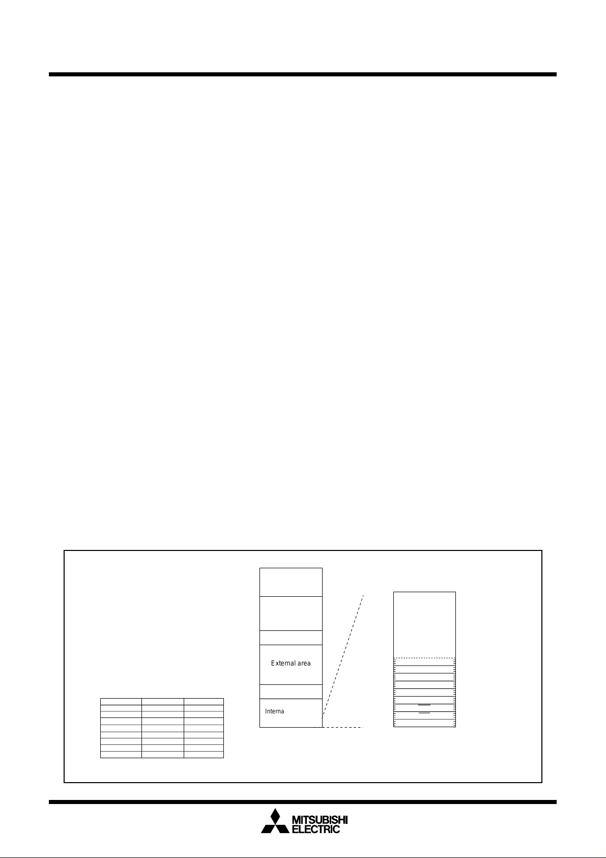
Figure 1.3.1 is a memory map of the M16C/62A group. The address space extends the 1M bytes from
address 0000016 to FFFFF16. From FFFFF16 down is ROM. For example, in the M30622MCA-XXXFP,
there is 128K bytes of internal ROM from E000016 to FFFFF16. The vector table for fixed interrupts such as
the reset and NMI are mapped to FFFDC16 to FFFFF16. The starting address of the interrupt routine is
stored here. The address of the vector table for timer interrupts, etc., can be set as desired using the
internal register (INTB). See the section on interrupts for details.
From 0040016 up is RAM. For example, in the M30622MCA-XXXFP, 5K bytes of internal RAM is mapped
to the space from 0040016 to 017FF16. In addition to storing data, the RAM also stores the stack used when
calling subroutines and when interrupts are generated.
The SFR area is mapped to 0000016 to 003FF16. This area accommodates the control registers for peripheral devices such as I/O ports, A-D converter, serial I/O, and timers, etc. Figures 1.6.1 to 1.6.3 are location
of peripheral unit control registers. Any part of the SFR area that is not occupied is reserved and cannot be
used for other purposes.
The special page vector table is mapped to FFE0016 to FFFDB16. If the starting addresses of subroutines
or the destination addresses of jumps are stored here, subroutine call instructions and jump instructions
can be used as 2-byte instructions, reducing the number of program steps.
In memory expansion mode and microprocessor mode, a part of the spaces are reserved and cannot be
used. For example, in the M30622MCA-XXXFP, the following spaces cannot be used.
• The space between 0180016 and 03FFF16 (Memory expansion and microprocessor modes)
• The space between D000016 and D7FFF16 (Memory expansion mode)
_______
Type No.
M30622M4A 00FFF
M30620M8A 02BFF
M30620MAA E8000
M30620MCA/FCA E0000
M30622M8A F0000
M30622MAA
M30622MCA
M30624MGA/FGA
Address XXXXX
Figure 1.3.1. Memory map
10
02BFF
02BFF
013FF
017FF
017FF
053FF
16
16
16
16
16
16
16
16
16
Address YYYYY
F8000
F0000
E8000
E0000
C0000
00000
16
SFR area
For details, see Figures
1.6.1 to 1.6.3
00400
16
Internal RAM area
XXXXX
16
Internal reserved
04000
area (Note 1)
16
AAA
External area
AAA
D0000
16
YYYYY
16
16
16
FFFFF
16
16
16
Note 1: During memory expansion and microprocessor modes, can not be used.
16
Note 2: In memory expansion mode, can not be used.
16
Note 3: These memory maps show an instance in which PM13 is set to 0; but in the
Internal reserved
16
area (Note 2)
16
Internal ROM area
16
case of M30624MGA/FGA, they show an instance in which PM13 is set to 1.
FFE00
FFFDC
FFFFF
16
Special page
vector table
16
Undefined instruction
Overflow
BRK instruction
Address match
Single step
Watchdog timer
16
DBC
NMI
Reset
Mitsubishi microcomputers
M16C / 62A Group
SINGLE-CHIP 16-BIT CMOS MICROCOMPUTER
CPU
A
Central Processing Unit (CPU)
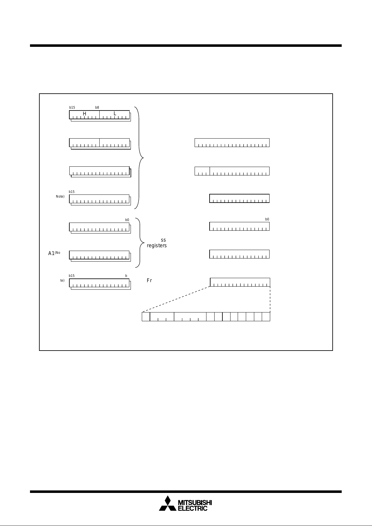
The CPU has a total of 13 registers shown in Figure 1.4.1. Seven of these registers (R0, R1, R2, R3, A0,
A1, and FB) come in two sets; therefore, these have two register banks.
R0
R1
R2
R3
A0
A1
FB
(Note)
(Note)
(Note)
(Note)
(Note)
(Note)
(Note)
b15
b15
b15
b15
b15
b15
b15
b8 b7 b0
H
b8 b7 b0
H
L
b19
L
PC
b0
Program counter
Data
b0
registers
INTB
b19
H
b0
L
Interrupt table
register
b0
b0
b15
USP
b15
ISP
b0
User stack pointer
b0
Interrupt stack
pointer
Address
b0
b0
registers
Frame base
registers
SB
FLG
b15
b15
b0
Static base
register
b0
Flag register
IPL
CDZSBOIU
Note: These registers consist of two register banks.
Figure 1.4.1. Central processing unit register
(1) Data registers (R0, R0H, R0L, R1, R1H, R1L, R2, and R3)
Data registers (R0, R1, R2, and R3) are configured with 16 bits, and are used primarily for transfer and
arithmetic/logic operations.
Registers R0 and R1 each can be used as separate 8-bit data registers, high-order bits as (R0H/R1H),
and low-order bits as (R0L/R1L). In some instructions, registers R2 and R0, as well as R3 and R1 can
use as 32-bit data registers (R2R0/R3R1).
(2) Address registers (A0 and A1)
Address registers (A0 and A1) are configured with 16 bits, and have functions equivalent to those of data
registers. These registers can also be used for address register indirect addressing and address register
relative addressing.
In some instructions, registers A1 and A0 can be combined for use as a 32-bit address register (A1A0).
11

Mitsubishi microcomputers
M16C / 62A Group
SINGLE-CHIP 16-BIT CMOS MICROCOMPUTER
CPU
(3) Frame base register (FB)
Frame base register (FB) is configured with 16 bits, and is used for FB relative addressing.
(4) Program counter (PC)
Program counter (PC) is configured with 20 bits, indicating the address of an instruction to be executed.
(5) Interrupt table register (INTB)
Interrupt table register (INTB) is configured with 20 bits, indicating the start address of an interrupt vector
table.
(6) Stack pointer (USP/ISP)
Stack pointer comes in two types: user stack pointer (USP) and interrupt stack pointer (ISP), each configured with 16 bits.
Your desired type of stack pointer (USP or ISP) can be selected by a stack pointer select flag (U flag).
This flag is located at the position of bit 7 in the flag register (FLG).
(7) Static base register (SB)
Static base register (SB) is configured with 16 bits, and is used for SB relative addressing.
(8) Flag register (FLG)
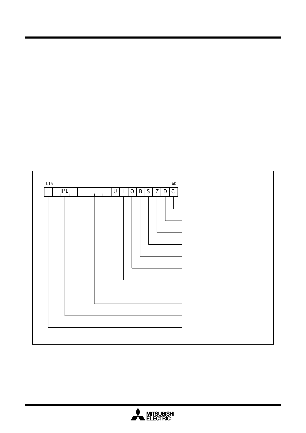
Flag register (FLG) is configured with 11 bits, each bit is used as a flag. Figure 1.4.2 shows the flag
register (FLG). The following explains the function of each flag:
• Bit 0: Carry flag (C flag)
This flag retains a carry, borrow, or shift-out bit that has occurred in the arithmetic/logic unit.
• Bit 1: Debug flag (D flag)
This flag enables a single-step interrupt.
When this flag is “1”, a single-step interrupt is generated after instruction execution. This flag is
cleared to “0” when the interrupt is acknowledged.
• Bit 2: Zero flag (Z flag)
This flag is set to “1” when an arithmetic operation resulted in 0; otherwise, cleared to “0”.
• Bit 3: Sign flag (S flag)
This flag is set to
• Bit 4: Register bank select flag (B flag)
This flag chooses a register bank. Register bank 0 is selected when this flag is “0” ; register bank 1 is
selected when this flag is “1”.
• Bit 5: Overflow flag (O flag)
This flag is set to “1” when an arithmetic operation resulted in overflow; otherwise, cleared to “0”.
• Bit 6: Interrupt enable flag (I flag)
This flag enables a maskable interrupt.
An interrupt is disabled when this flag is “0”, and is enabled when this flag is “1”. This flag is cleared to
“0” when the interrupt is acknowledged.
“1”
when an arithmetic operation resulted in a negative value; otherwise, cleared to
“0”
.
12
Mitsubishi microcomputers
M16C / 62A Group
SINGLE-CHIP 16-BIT CMOS MICROCOMPUTER
CPU
• Bit 7: Stack pointer select flag (U flag)
Interrupt stack pointer (ISP) is selected when this flag is “0” ; user stack pointer (USP) is selected
when this flag is “1”.
This flag is cleared to “0” when a hardware interrupt is acknowledged or an INT instruction of software
interrupt Nos. 0 to 31 is executed.
• Bits 8 to 11: Reserved area
• Bits 12 to 14: Processor interrupt priority level (IPL)
Processor interrupt priority level (IPL) is configured with three bits, for specification of up to eight
processor interrupt priority levels from level 0 to level 7.
If a requested interrupt has priority greater than the processor interrupt priority level (IPL), the interrupt
is enabled.
• Bit 15: Reserved area
The C, Z, S, and O flags are changed when instructions are executed. See the software manual for
details.
IPL
b0b15
Flag register (FLG)
CDZSBOIU
Carry flag
Debug flag
Zero flag
Sign flag
Register bank select flag
Overflow flag
Interrupt enable flag
Stack pointer select flag
Reserved area
Processor interrupt priority level
Reserved area
Figure 1.4.2. Flag register (FLG)
13
Mitsubishi microcomputer
s
p
R
M16C / 62A Grou
Reset
SINGLE-CHIP 16-BIT CMOS MICROCOMPUTE
Reset
There are two kinds of resets; hardware and software. In both cases, operation is the same after the reset.
(See “Software Reset” for details of software resets.) This section explains on hardware resets.
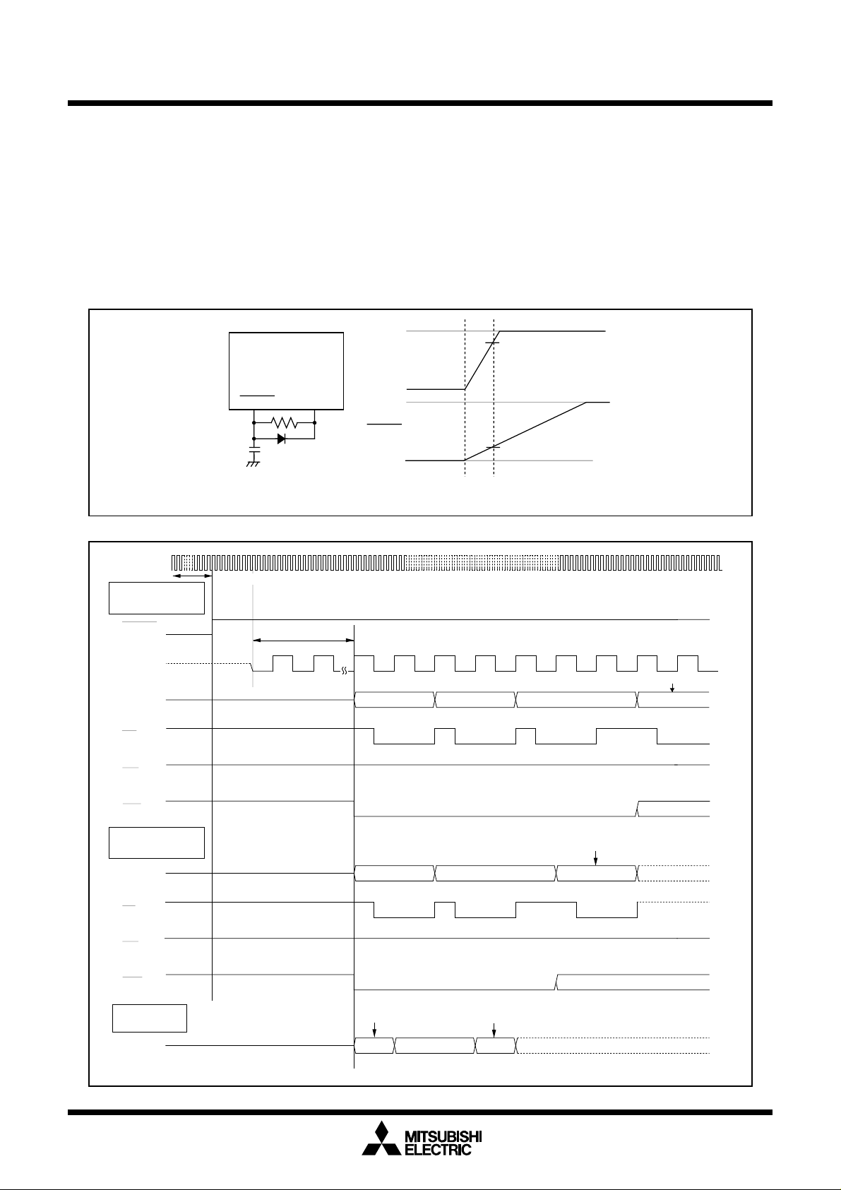
When the supply voltage is in the range where operation is guaranteed, a reset is effected by holding the
reset pin level “L” (0.2VCC max.) for at least 20 cycles. When the reset pin level is then returned to the “H”
level while main clock is stable, the reset status is cancelled and program execution resumes from the
address in the reset vector table.
Figure 1.5.1 shows the example reset circuit. Figure 1.5.2 shows the reset sequence.
RESET
Example when V
V
CC
Figure 1.5.1. Example reset circuit
X
IN
More than 20 cycles are needed
Microprocessor
mode BYTE = “H”
RESET
BCLK
Address
RD
BCLK 24cycles
CC
= 5V
5V
V
CC
0V
5V
RESET
0V
4.0V
0.8V
.
Content of reset vector
FFFFC
16
FFFFD
16
FFFFE
16
WR
CS0
Microprocessor
mode BYTE = “L”
Address
RD
WR
CS0
Single chip
mode
Address
Figure 1.5.2. Reset sequence
14
Content of reset vector
FFFFC
FFFFC
16
16
FFFFE
FFFFE
16
Content of reset vector
16
s
p
R
Reset
Mitsubishi microcomputer
M16C / 62A Grou
SINGLE-CHIP 16-BIT CMOS MICROCOMPUTE
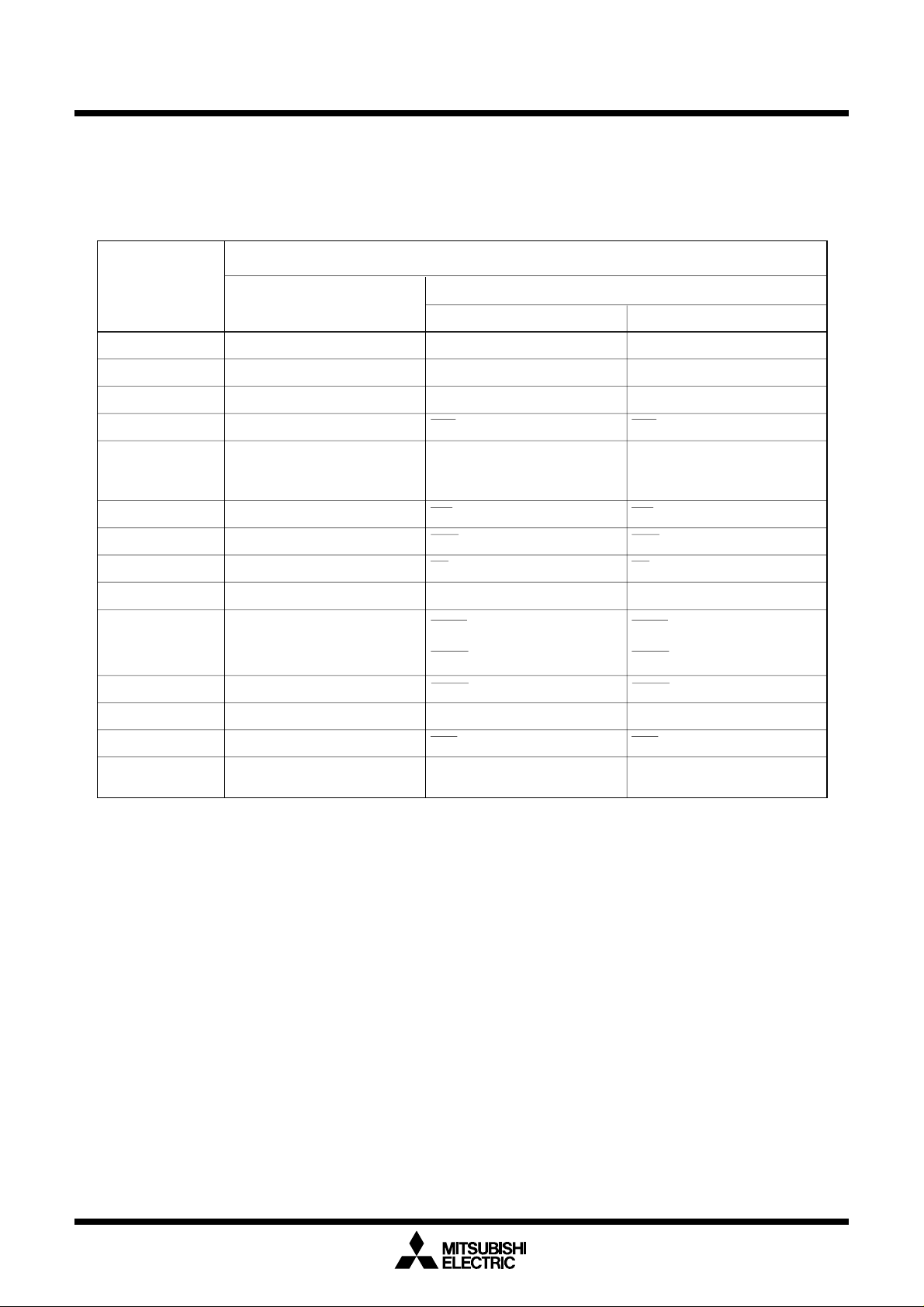
Table 1.5.1 shows the statuses of the other pins while the RESET pin level is “L”. Figures 1.5.3 and 1.5.4
____________
show the internal status of the microcomputer immediately after the reset is cancelled.
Table 1.5.1. Pin status when RESET pin level is “L”
____________
Status
Pin name
P0
P1
P2, P3, P4
P4
4
P45 to P4
P5
0
P5
1
P5
2
0
7
to P4
CNVSS = V
Input port (floating)
Input port (floating)
Input port (floating)
3
Input port (floating)
Input port (floating)
Input port (floating)
Input port (floating)
Input port (floating)
SS
CNVSS = V
BYTE = V
SS
Data input (floating)
Data input (floating)
Address output (undefined)
CS0 output (“H” level is output)
Input port (floating)
(pull-up resistor is on)
WR output (“H” level is output)
BHE output (undefined)
RD output (“H” level is output)
CC
BYTE = V
CC
Data input (floating)
Input port (floating)
Address output (undefined)
CS0 output (“H” level is output)
Input port (floating)
(pull-up resistor is on)
WR output (“H” level is output)
BHE output (undefined)
RD output (“H” level is output)
P5
3
P5
4
P5
5
P5
6
P5
7
P6, P7, P80 to P84,
6
, P87, P9, P10
P8
Input port (floating)
Input port (floating)
Input port (floating)
Input port (floating)
Input port (floating)
Input port (floating)
BCLK output
HLDA output (The output value
depends on the input to the
HOLD pin)
HOLD input (floating)
ALE output (“L” level is output)
RDY input (floating)
BCLK output
HLDA output (The output value
depends on the input to the
HOLD pin)
HOLD input (floating)
ALE output (“L” level is output)
RDY input (floating)
Input port (floating) Input port (floating)
15
s
p
R
Reset
16
(1) (0004
)···Processor mode register 0 (Note 1) 00
(2) (000516)···Processor mode register 1 000
16
(3) (0006
(4) (0007
(5) (0008
(6) (0009
Address match interrupt enable register
(7) Protect register (000A
(8)
(9)
(10)
(11)
(12)
(13)
(14)
(15)
(16)
(17)
(18)
Bus collision detection interrupt
(19)
control register
(20)
(21)
(22)
(23)
A-D conversion interrupt control register
(24)
UART2 transmit interrupt control register
(25)
UART2 receive interrupt control register
(26)
UART0 transmit interrupt control register
UART0 receive interrupt control register
(27)
(28)
UART1 transmit interrupt control register
)···System clock control register 0 10000100
16
)···System clock control register 1 00010000
16
)···Chip select control register 00000010
16
)···
16
)···
(000F16)···Watchdog timer control register 00?0????
16
)···Address match interrupt register 0
(0010
16
)···
(0011
16
)··· 0
(0012
16
)···Address match interrupt register 1
(0014
16
)···
(0015
(0016
16
)··· 0
16
)···DMA0 control register 00000?00
(002C
16
)···DMA1 control register 00000?00
(003C
(0044
16
)···INT3 interrupt control register 00?000
16
)···Timer B5 interrupt control register ?000
(0045
16
)···Timer B4 interrupt control register ?000
(0046
16
)···Timer B3 interrupt control register ?000
(0047
(0048
16
)···SI/O4 interrupt control register
16
)···SI/O3 interrupt control register
(0049
16
)···
(004A
(004B
16
)···DMA0 interrupt control register ? 0 0 0
16
)···DMA1 interrupt control register ? 0 0 0
(004C
16
)···Key input interrupt control register ? 0 0 0
(004D
16
)··· ? 0 0 0
(004E
(004F
16
)···
16
)···
(0050
(0051
16
)···
(0052
16
)···
16
)···
(0053
16
000
000
00
16
00
16
0 0 0
00
16
00
16
0 0 0
00?000
00?000
0 0 0?
? 0 0 0
? 0 0 0
? 0 0 0
? 0 0 0
? 0 0 0
SINGLE-CHIP 16-BIT CMOS MICROCOMPUTE
(29)
UART1 receive interrupt control register
(30)
Timer A0 interrupt control register
(31)
Timer A1 interrupt control register
(32)
Timer A2 interrupt control register
(33)
Timer A3 interrupt control register
(34)
00
Timer A4 interrupt control register
(35)
Timer B0 interrupt control register
(36)
Timer B1 interrupt control register
(37)
Timer B2 interrupt control register
(38)
INT0 interrupt control register
(39)
INT1 interrupt control register
(40)
INT2 interrupt control register
(41)
Timer B3,4,5 count start flag
(42)
Three-phase PWM control register 0
(43)
Three-phase PWM control register 1
(44)
Three-phase output buffer register 0
(45)
Three-phase output buffer register 1
(46)
Timer B3 mode register
(47)
Timer B4 mode register
(48)
Timer B5 mode register
(49)
Interrupt cause select register
(50)
(51)
SI/O4 control register
(52)
UART2 special mode register 3 (Note 2) (037516)···
UART2 special mode register 2 (0376
(53)
UART2 special mode register
(54)
(55)
UART2 transmit/receive mode register
(56)
UART2 transmit/receive control register 0
(57)
UART2 transmit/receive control register 1
Mitsubishi microcomputer
M16C / 62A Grou
16
(0054
(0055
(0056
(0057
(0058
(0059
(005A
(005B
(005C
(005D
(005E
(005F
(0340
(0348
(0349
(034A
(034B
(035B
(035C
(035D
(035F
(0362
(0366
(0377
(0378
(037C
(037D
)···
16
)···
16
)···
16
)···
16
)···
16
)···
16
)···
16
)···
16
)···
16
)···
16
)···
16
)···
16
)···
16
)···
16
)···
16
)···
16
)···
16
)···
16
)···
16
)···
16
)···
16
)···SI/O3 control register
16
)···
16
)···
16
)···
16
)···
16
)···
16
)···
? 0 0 0
? 0 0 0
? 0 0 0
? 0 0 0
? 0 0 0
? 0 0 0
? 0 0 0
? 0 0 0
? 0 0 0
? 00000
? 00000
? 00000
000
00
16
00
16
00
16
00
16
00? 0000
00? 0000
00? 0000
00
16
40
16
40
16
?
00
16
00
16
00
16
00000001
01000000
x : Nothing is mapped to this bit
? : Undefined
The content of other registers and RAM is undefined when the microcomputer is reset. The initial values must therefore be set.
Note 1: When the V
Note 2: “00
CC
16
level is applied to the CNVSS pin, it is 0316 at a reset.
” is read out when set bit 7 (SDDS) of the UART2 special mode register ( address 037716) to “1”.
Figure 1.5.3. Device's internal status after a reset is cleared
16
s
p
R
Reset
Mitsubishi microcomputer
M16C / 62A Grou
SINGLE-CHIP 16-BIT CMOS MICROCOMPUTE
(58)
Count start flag (0380
(59)
(61)
(65)
(67)
(69)
(79)
(80)
(81)
(82)
(83)
16
16
)··· 00
16
)···Clock prescaler reset flag
(0381
16
)···One-shot start flag(60)
(0382
(038316)···Trigger select flag
16
)···Up-down flag(62)
(0384
(0396
16
)···Timer A0 mode register(63)
16
)···Timer A1 mode register(64)
(0397
(0398
16
)···Timer A2 mode register
16
)···Timer A3 mode register(66)
(0399
(039A
16
)···Timer A4 mode register
(039B
16
)···Timer B0 mode register(68)
16
)···Timer B1 mode register
(039C
(039D
16
)···Timer B2 mode register(70)
16
)···UART0 transmit/receive mode register(71)
(03A0
(03A4
16
)···UART0 transmit/receive control register 0(72)
(03A5
16
)···UART0 transmit/receive control register 1(73)
(03A8
16
)···UART1 transmit/receive mode register(74) 00
(03AC
16
)···UART1 transmit/receive control register 0(75)
(03AD
16
)···UART1 transmit/receive control register 1(76)
(03B0
16
)···UART transmit/receive control register 2(77) 0
(03B6
16
)···Flash memory control register 1 (Note2)(78)
(03B7
16
)···Flash memory control register 0 (Note2)
16
)···DMA0 cause select register
(03B8
(03BA
16
)···DMA1 cause select register 00
(03D416)···A-D control register 2
(03D6
16
)···A-D control register 0
The content of other registers and RAM is undefined when the microcomputer is reset. The initial values
must therefore be set.
Note1: When the V
Note2: This register is only exist in flash memory version.
16
0
0000 000
00
16
00
16
00
16
00
16
00
16
00
16
00
16
0
0? 0000
00? 0000
00? 0000
00
16
000 1000
0
000 0010
0
16
000 1000
0
000 0010
0
0 00000
0
???? ???
0 00010
00
16
16
0000
(84)
(85)
(86)
(87)
(88)
(89)
(90)
(91)
(92)
(93)
(94)
(95)
(96)
(97)
(98)
(99)
(100)
Port control register
(101)
Data registers (R0/R1/R2/R3)
(102)
Address registers (A0/A1)
(103)
Frame base register (FB)
(104)
Interrupt table register (INTB)
(105)
User stack pointer (USP)
(106)
Interrupt stack pointer (ISP)
Static base register (SB)
(107)
Flag register (FLG)
(108)
0
000 0???0
x : Nothing is mapped to this bit
? : Undefined
CC
level is applied to the CNVSS pin, it is 0216 at a reset.
(03D7
16
(03DC
16
(03E2
16
(03E3
(03E6
16
(03E7
16
(03EA
16
(03EB
16
(03EE
16
(03EF
16
16
(03F2
(03F3
16
(03F6
16
(03FC
16
16
(03FD
(03FE
16
(03FF16)···
)···A-D control register 1 00
)···D-A control register
)···Port P0 direction register
)···Port P1 direction register
)···Port P2 direction register
)···Port P3 direction register
)···Port P4 direction register
)···Port P5 direction register
)···Port P6 direction register
)···Port P7 direction register
)···Port P8 direction register
)···Port P9 direction register
)···Port P10 direction register
)···Pull-up control register 0
)···Pull-up control register 1(Note1)
)···Pull-up control register 2
16
00
16
00
16
00
16
00
16
00
16
00
16
00
16
00
16
00
16
00 00000
00
16
00
16
00
16
00
16
00
16
00
16
0000
0000
0000
00000
0000
0000
0000
0000
16
16
16
16
16
16
16
16
Figure 1.5.4. Device's internal status after a reset is cleared
17
s
p
R
SFR
Mitsubishi microcomputer
M16C / 62A Grou
SINGLE-CHIP 16-BIT CMOS MICROCOMPUTE
000016
000116
000216
000316
Processor mode register 0 (PM0)
000416
000516
Processor mode register 1(PM1)
000616
System clock control register 0 (CM0)
000716
System clock control register 1 (CM1)
000816
Chip select control register (CSR)
000916
Address match interrupt enable register (AIER)
000A16
Protect register (PRCR)
000B16
000C16
000D16
000E16
Watchdog timer start register (WDTS)
Watchdog timer control register (WDC)
000F16
001016
001116
Address match interrupt register 0 (RMAD0)
001216
001316
001416
Address match interrupt register 1 (RMAD1)
001516
001616
001716
001816
001916
001A16
001B16
001C16
001D16
001E16
001F16
002016
DMA0 source pointer (SAR0)
002116
002216
002316
002416
002516
DMA0 destination pointer (DAR0)
002616
002716
002816
DMA0 transfer counter (TCR0)
002916
002A16
002B16
002C16
DMA0 control register (DM0CON)
002D16
002E16
002F16
003016
DMA1 source pointer (SAR1)
003116
003216
003316
003416
DMA1 destination pointer (DAR1)
003516
003616
003716
003816
DMA1 transfer counter (TCR1)
003916
003A16
003B16
003C16
DMA1 control register (DM1CON)
003D16
003E16
003F16
004016
004116
004216
004316
INT3 interrupt control register (INT3IC)
004416
004516
Timer B5 interrupt control register (TB5IC)
Timer B4 interrupt control register (TB4IC)
004616
Timer B3 interrupt control register (TB3IC)
004716
SI/O4 interrupt control register (S4IC)
004816
INT5 interrupt control register (INT5IC)
SI/O3 interrupt control register (S3IC)
004916
INT4 interrupt control register (INT4IC)
Bus collision detection interrupt control register (BCNIC)
004A16
DMA0 interrupt control register (DM0IC)
004B16
004C16
DMA1 interrupt control register (DM1IC)
Key input interrupt control register (KUPIC)
004D16
A-D conversion interrupt control register (ADIC)
004E16
UART2 transmit interrupt control register (S2TIC)
004F16
UART2 receive interrupt control register (S2RIC)
005016
UART0 transmit interrupt control register (S0TIC)
005116
UART0 receive interrupt control register (S0RIC)
005216
UART1 transmit interrupt control register (S1TIC)
005316
UART1 receive interrupt control register (S1RIC)
005416
Timer A0 interrupt control register (TA0IC)
005516
Timer A1 interrupt control register (TA1IC)
005616
Timer A2 interrupt control register (TA2IC)
005716
Timer A3 interrupt control register (TA3IC)
005816
Timer A4 interrupt control register (TA4IC)
005916
Timer B0 interrupt control register (TB0IC)
005A16
Timer B1 interrupt control register (TB1IC)
005B16
Timer B2 interrupt control register (TB2IC)
005C16
INT0 interrupt control register (INT0IC)
005D16
INT1 interrupt control register (INT1IC)
005E16
INT2 interrupt control register (INT2IC)
005F16
006016
006116
006216
006316
006416
006516
032A16
032B16
032C16
032D16
032E16
032F16
033016
033116
033216
033316
033416
033516
033616
033716
033816
033916
033A16
033B16
033C16
033D16
033E16
033F16
Note 1: Locations in the SFR area where nothing is allocated are reserved areas. Do not access these areas for read or write.
Figure 1.6.1. Location of peripheral unit control registers (1)
18
s
p
R
SFR
0340
16
Timer B3, 4, 5 count start flag (TBSR)
0341
16
0342
16
Timer A1-1 register (TA11)
0343
16
0344
16
Timer A2-1 register (TA21)
0345
16
0346
16
Timer A4-1 register (TA41)
0347
16
0348
16
Three-phase PWM control register 0(INVC0)
0349
16
Three-phase PWM control register 1(INVC1)
034A
16
Three-phase output buffer register 0(IDB0)
034B
16
Three-phase output buffer register 1(IDB1)
034C
16
Dead time timer(DTT)
Timer B2 interrupt occurrence frequency set counter(ICTB2)
034D
16
034E
16
034F
16
0350
16
Timer B3 register (TB3)
0351
16
0352
16
Timer B4 register (TB4)
0353
16
0354
16
Timer B5 register (TB5)
0355
16
0356
16
0357
16
0358
16
0359
16
035A
16
035B
16
Timer B3 mode register (TB3MR)
035C
16
Timer B4 mode register (TB4MR)
035D
16
Timer B5 mode register (TB5MR)
035E
16
035F
16
Interrupt cause select register (IFSR)
transmit/receive register
SI/O3
0360
16
0361
16
SI/O3 control register (S3C)
0362
0363
0364
0365
0366
0367
0368
0369
036A
036B
036C
036D
036E
036F
0370
0371
0372
0373
0374
0375
0376
0377
0378
0379
037A
037B
037C
037D
037E
037F
16
16
16
16
16
16
16
16
16
16
16
16
16
16
16
16
16
16
16
16
16
16
16
16
16
16
16
16
16
16
bit rate generator
SI/O3
SI/O4
transmit/receive register
(S3BRG)
SI/O4 control register (S4C)
SI/O4
bit rate generator
(S4BRG)
UART2 special mode register 3(U2SMR3)
UART2 special mode register 2(U2SMR2)
UART2 special mode register (U2SMR)
UART2 transmit/receive mode register (U2MR)
UART2 bit rate generator (U2BRG)
UART2 transmit buffer register (U2TB)
UART2 transmit/receive control register 0 (U2C0)
UART2 transmit/receive control register 1 (U2C1)
UART2 receive buffer register (U2RB)
(S3TRR)
(S4TRR)
SINGLE-CHIP 16-BIT CMOS MICROCOMPUTE
M16C / 62A Grou
0380
16
Count start flag (TABSR)
0381
16
Clock prescaler reset flag (CPSRF)
0382
16
One-shot start flag (ONSF)
0383
16
Trigger select register (TRGSR)
0384
16
Up-down flag (UDF)
0385
16
0386
16
Timer A0 (TA0)
0387
16
0388
16
Timer A1 (TA1)
0389
16
038A
16
Timer A2 (TA2)
038B
16
038C
16
Timer A3 (TA3)
038D
16
038E
16
Timer A4 (TA4)
038F
16
0390
16
Timer B0 (TB0)
0391
16
0392
16
Timer B1 (TB1)
0393
16
0394
16
Timer B2 (TB2)
0395
16
0396
16
Timer A0 mode register (TA0MR)
0397
16
Timer A1 mode register (TA1MR)
0398
16
Timer A2 mode register (TA2MR)
0399
16
Timer A3 mode register (TA3MR)
039A
16
Timer A4 mode register (TA4MR)
039B
16
Timer B0 mode register (TB0MR)
039C
16
Timer B1 mode register (TB1MR)
039D
16
Timer B2 mode register (TB2MR)
039E
16
039F
16
03A0
16
UART0 transmit/receive mode register (U0MR)
03A1
16
UART0 bit rate generator (U0BRG)
03A2
16
UART0 transmit buffer register (U0TB)
03A3
16
03A4
16
UART0 transmit/receive control register 0 (U0C0)
03A5
16
UART0 transmit/receive control register 1 (U0C1)
03A6
16
UART0 receive buffer register (U0RB)
03A7
16
03A8
16
UART1 transmit/receive mode register (U1MR)
03A9
16
UART1 bit rate generator (U1BRG)
03AA
16
UART1 transmit buffer register (U1TB)
03AB
16
03AC
16
UART1 transmit/receive control register 0 (U1C0)
UART1 transmit/receive control register 1 (U1C1)
03AD
16
03AE
16
UART1 receive buffer register (U1RB)
03AF
16
03B0
16
UART transmit/receive control register 2 (UCON)
03B1
16
03B2
16
03B3
16
03B4
16
03B5
16
Flash memory control register 1 (FMR1) (Note1)
03B6
16
03B7
16
Flash memory control register 0 (FMR0) (Note1)
03B8
16
DMA0 request cause select register (DM0SL)
03B9
16
03BA
16
DMA1 request cause select register (DM1SL)
03BB
16
03BC
16
CRC data register (CRCD)
03BD
16
CRC input register (CRCIN)
03BE
16
03BF
16
Mitsubishi microcomputer
Note 1: This register is only exist in flash memory version.
Note 2: Locations in the SFR area where nothing is allocated are reserved areas. Do not access these areas for
read or write.
Figure 1.6.2. Location of peripheral unit control registers (2)
19
s
p
R
SFR
03C016
A-D register 0 (AD0)
03C116
03C216
A-D register 1 (AD1)
03C316
03C416
A-D register 2 (AD2)
03C516
03C616
A-D register 3 (AD3)
03C716
03C816
A-D register 4 (AD4)
03C916
03CA16
A-D register 5 (AD5)
03CB16
03CC16
A-D register 6 (AD6)
03CD16
03CE16
A-D register 7 (AD7)
03CF16
03D016
03D116
03D216
03D316
03D416
A-D control register 2 (ADCON2)
03D516
03D616
A-D control register 0 (ADCON0)
03D716
A-D control register 1 (ADCON1)
03D816
D-A register 0 (DA0)
03D916
03DA16
D-A register 1 (DA1)
03DB16
03DC16
D-A control register (DACON)
03DD16
03DE16
03DF16
03E016
Port P0 (P0)
03E116
Port P1 (P1)
03E216
Port P0 direction register (PD0)
03E316
Port P1 direction register (PD1)
03E416
Port P2 (P2)
03E516
Port P3 (P3)
03E616
Port P2 direction register (PD2)
03E716
Port P3 direction register (PD3)
03E816
Port P4 (P4)
03E916
Port P5 (P5)
03EA16
Port P4 direction register (PD4)
03EB16
Port P5 direction register (PD5)
03EC16
Port P6 (P6)
03ED16
Port P7 (P7)
03EE16
Port P6 direction register (PD6)
03EF16
Port P7 direction register (PD7)
03F016
Port P8 (P8)
03F116
Port P9 (P9)
03F216
Port P8 direction register (PD8)
03F316
Port P9 direction register (PD9)
03F416
Port P10 (P10)
03F516
03F616
Port P10 direction register (PD10)
03F716
03F816
03F916
03FA16
03FB16
03FC16
Pull-up control register 0 (PUR0)
03FD16
Pull-up control register 1 (PUR1)
03FE16
Pull-up control register 2 (PUR2)
Port control register (PCR)
03FF16
Mitsubishi microcomputer
M16C / 62A Grou
SINGLE-CHIP 16-BIT CMOS MICROCOMPUTE
Note : Locations in the SFR area where nothing is allocated are reserved
areas. Do not access these areas for read or write.
Figure 1.6.3. Location of peripheral unit control registers (3)
20

Mitsubishi microcomputer
s
p
R
M16C / 62A Grou
Software Reset
Software Reset
SINGLE-CHIP 16-BIT CMOS MICROCOMPUTE
Software Reset
Writing “1” to bit 3 of the processor mode register 0 (address 000416) applies a (software) reset to the
microcomputer. A software reset has the same effect as a hardware reset. The contents of internal RAM
are preserved.
Processor Mode
(1) Types of Processor Mode
One of three processor modes can be selected: single-chip mode, memory expansion mode, and microprocessor mode. The functions of some pins, the memory map, and the access space differ according to
the selected processor mode.
• Single-chip mode
In single-chip mode, only internal memory space (SFR, internal RAM, and internal ROM) can be
accessed. However, after the reset has been released and the operation of shifting from the microprocessor mode has started (“H” applied to the CNVSS pin), the internal ROM area cannot be accessed
even if the CPU shifts to the single-chip mode.
Ports P0 to P10 can be used as programmable I/O ports or as I/O ports for the internal peripheral
functions.
• Memory expansion mode
In memory expansion mode, external memory can be accessed in addition to the internal memory
space (SFR, internal RAM, and internal ROM). However, after the reset has been released and the
operation of shifting from the microprocessor mode has started (“H” applied to the CNVSS pin), the
internal ROM area cannot be accessed even if the CPU shifts to the memory expansion mode.
In this mode, some of the pins function as the address bus, the data bus, and as control signals. The
number of pins assigned to these functions depends on the bus and register settings. (See “Bus
Settings” for details.)
• Microprocessor mode
In microprocessor mode, the SFR, internal RAM, and external memory space can be accessed. The
internal ROM area cannot be accessed.
In this mode, some of the pins function as the address bus, the data bus, and as control signals. The
number of pins assigned to these functions depends on the bus and register settings. (See “Bus
Settings” for details.)
(2) Setting Processor Modes
The processor mode is set using the CNVSS pin and the processor mode bits (bits 1 and 0 at address
000416). Do not set the processor mode bits to “102”.
Regardless of the level of the CNVSS pin, changing the processor mode bits selects the mode. Therefore,
never change the processor mode bits when changing the contents of other bits. Also do not attempt to
shift to or from the microprocessor mode within the program stored in the internal ROM area.
• Applying VSS to CNVSS pin
The microcomputer begins operation in single-chip mode after being reset. Memory expansion mode
is selected by writing “012” to the processor mode is selected bits.
• Applying VCC to CNVSS pin
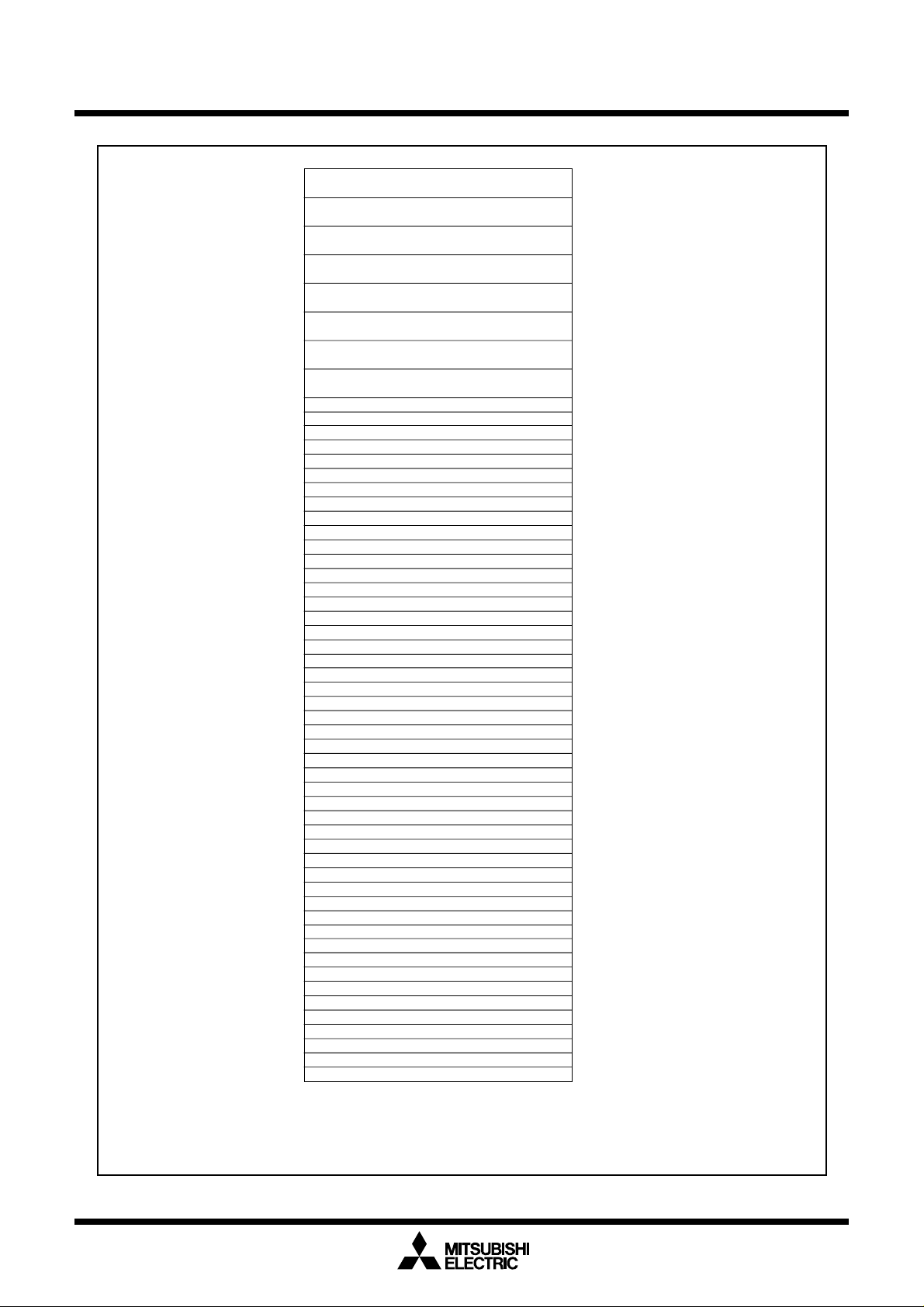
The microcomputer starts to operate in microprocessor mode after being reset.
Figure 1.7.1 shows the processor mode register 0 and 1.
Figure 1.7.2 shows the memory maps applicable for each of the modes.
21
Mitsubishi microcomputers
M16C / 62A Group
SINGLE-CHIP 16-BIT CMOS MICROCOMPUTER
Processor Mode
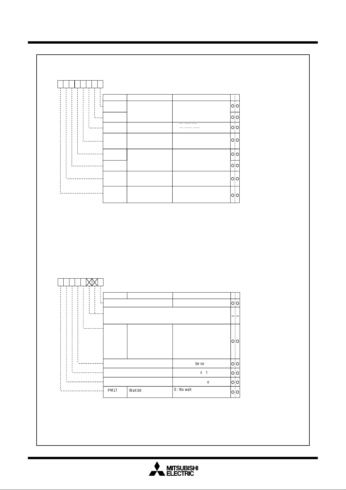
Processor mode register 0 (Note 1)
b7 b6 b5 b4 b3 b2 b1 b0
Symbol Address When reset
PM0 0004
16
00
16
(Note 2)
Bit name FunctionBit symbol
PM00
PM01
PM02
PM03
PM04
PM05
PM06
PM07
Note 1: Set bit 1 of the protect register (address 000A
Note 2: If the V
Note 3: Valid in microprocessor and memory expansion modes.
Note 4: If the entire space is of multiplexed bus in memory expansion mode, choose an 8-
Processor mode bit
R/W mode select bit
Software reset bit
Multiplexed bus space
select bit
Port P40 to P43 function
select bit (Note 3)
BCLK output disable bit
values to this register.
CC
voltage is applied to the CNVSS, the value of this register when
reset is 03
16
. (PM00 and PM01 both are set to “1”.)
bit width.The processor operates using the separate bus after reset is revoked, so the entire
space multiplexed bus cannot be chosen in microprocessor mode.
The higher-order address becomes a port if the entire space multiplexed bus is chosen, so
only 256 bytes can be used in each chip select.
b1 b0
0 0: Single-chip mode
0 1: Memory expansion mode
1 0: Inhibited
1 1: Microprocessor mode
0 : RD,BHE,WR
1 : RD,WRH,WRL
The device is reset when this bit is set
to “1”. The value of this bit is “0” when
read.
b5 b4
0 0 : Multiplexed bus is not used
0 1 : Allocated to CS2 space
1 0 : Allocated to CS1 space
1 1 : Allocated to entire space (Note4)
0 : Address output
1 : Port function
(Address is not output)
0 : BCLK is output
1 : BCLK is not output
(Pin is left floating)
16
) to “1” when writing new
WR
Processor mode register 1 (Note 1)
b7 b6 b5 b4 b3 b2 b1 b0
00
0
Symbol Address When reset
PM1 0005
0
Reserved bit
Nothing is assigned.
In an attempt to write to these bits, write “0”. The value, if read, turns
out to be
indeterminate.
PM13
Reserved bit
Reserved bit
Reserved bit
PM17 Wait bit
Note 1: Set bit 1 of the protect register (address 000A
Note 2: Be sure to set this bit to 0 except products whose RAM size and ROM size exceed 15K bytes
Internal reserved area
expansion bit (Note 2)
and 192K bytes respectively.
In using M30624MAG/FGA, a product having a RAM of more than 15K bytes and a ROM of
more than 192K bytes, set this bit to “1” at the beginning of user program.
Specify D0000
to “0” at the time reset is revoked, for the reset vector table of user program.
16
Bit name FunctionBit symbol
00000XX0
2
WR
Must always be set to “0”
0: The same internal reserved
area as that of M16C/60 and
M16C/61 group
1: Expands the internal RAM area
and internal ROM area to 23 K
bytes and to 256K bytes
respectively. (Note 2)
Must always be set to “0”
Must always be set to “0”
Must always be set to “0”
0 : No wait state
1 : Wait state inserted
16
) to “1” when writing new values to this register.
16
or a subsequent address, which becomes an internal ROM area if PM13 is set
Figure 1.7.1. Processor mode register 0 and 1
22
s
p
R
Processor Mode
Mitsubishi microcomputer
M16C / 62A Grou
SINGLE-CHIP 16-BIT CMOS MICROCOMPUTE
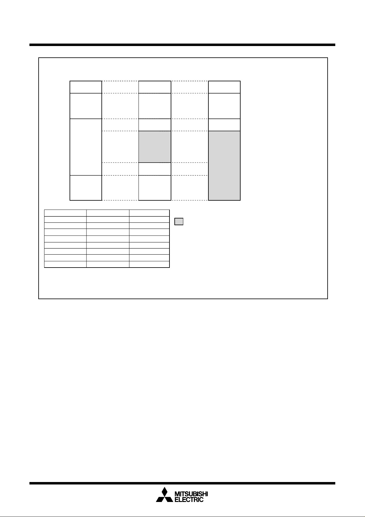
Single-chip mode
16
00000
00400
XXXXX
04000
D0000
YYYYY
FFFFF
M30622M4A 00FFF
M30620M8A 02BFF
M30620MAA E8000
M30620MCA/FCA E0000
M30622M8A F0000
M30622MAA
M30622MCA
M30624MGA/FGA
16
16
16
16
16
16
Type No.
SFR area
Internal
RAM area
Inhibited
Internal
ROM area
Address XXXXX
02BFF
02BFF
013FF
017FF
017FF
053FF
Memory expansion mode
SFR area
Internal
RAM area
Internally
reserved area
External
Internally
reserved area
Internal
ROM area
16
Address YYYYY
16
16
16
16
16
16
16
16
F8000
F0000
E8000
E0000
C0000
area
16
16
16
16
Microprocessor mode
SFR area
Internal
RAM area
Internally
reserved area
External
area
16
External area : Accessing this area allows the user to
access a device connected externally
to the microcomputer.
16
16
16
16
Note : These memory maps show an instance in which PM13 is set to 0; but in the case of M30624MGA/FGA,
they show an instance in which PM13 is set to 1.
Figure 1.7.2. Memory maps in each processor mode (without memory area expansion, normal mode)
23
Mitsubishi microcomputers
M16C / 62A Group
SINGLE-CHIP 16-BIT CMOS MICROCOMPUTER
Processor Mode
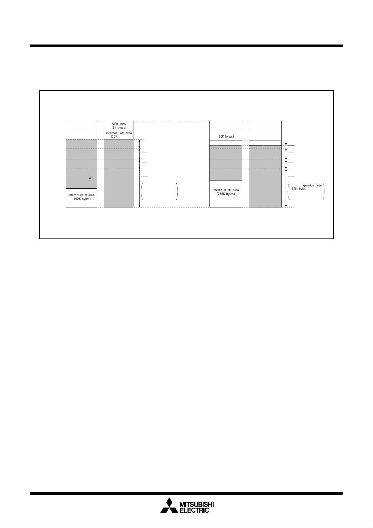
Figure 1.7.3 shows the memory maps and the chip selection areas effected by PM13 (the internal reserved
area expansion bit) in each processor mode for the product having an internal RAM of more than 15K bytes
and a ROM of more than 192K bytes.
Internal reserved area expansion bit=“0”
00000
00400
04000
08000
28000
30000
CFFFF
D0000
FFFFF
16
16
16
16
16
16
16
16
16
Memory expansion
mode
SFR area
(1K bytes)
Internal RAM area
(15K bytes)
External area
Internal ROM area
(192K bytes)
After reset
Microprocessor
mode
SFR area
(1K bytes)
Internal RAM area
(15K bytes)
External area
(16K bytes)
CS3
(128K bytes)
CS2
(32K bytes)
CS1
CS0
Memory expansion mode
: 640K bytes
Microprocessor mode
: 832K bytes
Figure 1.7.3. Memory location and chip select area
Internal reserved area expansion bit=“1”
Memory expansion
00000
16
SFR area
00400
05400
06000
08000
28000
30000
BFFFF
C0000
FFFFF
After reset, and set the
(1K bytes)
16
Internal RAM area
(20K bytes)
16
Internal reserved area
16
16
16
16
External area
16
16
Internal ROM area
(256K bytes)
16
mode
I
nternal reserved area expansion bit to “1”
Microprocessor
mode
SFR area
(1K bytes)
Internal RAM area
(20K bytes)
Internal reserved area
External area
(8K bytes)
CS3
(128K bytes)
CS2
(32K bytes)
CS1
CS0
Memory expansion mode
: 576K bytes
Microprocessor mode
: 832K bytes
Note: The reset vector lies in an area between D000016 and FFFFB16.
in each processor mode
24

Mitsubishi microcomputer
s
p
R
M16C / 62A Grou
Bus Settings
SINGLE-CHIP 16-BIT CMOS MICROCOMPUTE
Bus Settings
The BYTE pin and bits 4 to 6 of the processor mode register 0 (address 000416) are used to change the bus settings.
Table 1.8.1 shows the factors used to change the bus settings.
Table 1.8.1. Factors for switching bus settings
Bus setting Switching factor
Switching external address bus width Bit 6 of processor mode register 0
Switching external data bus width BYTE pin
Switching between separate and multiplex bus Bits 4 and 5 of processor mode register 0
(1) Selecting external address bus width
The address bus width for external output in the 1M bytes of address space can be set to 16 bits (64K
bytes address space) or 20 bits (1M bytes address space). When bit 6 of the processor mode register 0
is set to “1”, the external address bus width is set to 16 bits, and P2 and P3 become part of the address
bus. P40 to P43 can be used as programmable I/O ports. When bit 6 of processor mode register 0 is set
to “0”, the external address bus width is set to 20 bits, and P2, P3, and P40 to P43 become part of the
address bus.
(2) Selecting external data bus width
The external data bus width can be set to 8 or 16 bits. (Note, however, that only the separate bus can be
set.) When the BYTE pin is “L”, the bus width is set to 16 bits; when “H”, it is set to 8 bits. (The internal bus
width is permanently set to 16 bits.) While operating, fix the BYTE pin either to “H” or to “L”.
(3) Selecting separate/multiplex bus
The bus format can be set to multiplex or separate bus using bits 4 and 5 of the processor mode register 0.
• Separate bus
In this mode, the data and address are input and output separately. The data bus can be set using the
BYTE pin to be 8 or 16 bits. When the BYTE pin is “H”, the data bus is set to 8 bits and P0 functions as
the data bus and P1 as a programmable I/O port. When the BYTE pin is “L”, the data bus is set to 16
bits and P0 and P1 are both used for the data bus.
When the separate bus is used for access, a software wait can be selected.
• Multiplex bus
In this mode, data and address I/O are time multiplexed. With an 8-bit data bus selected (BYTE pin =
“H”), the 8 bits from D0 to D7 are multiplexed with A0 to A7.
With a 16-bit data bus selected (BYTE pin = “L”), the 8 bits from D0 to D7 are multiplexed with A1 to A8.
D8 to D15 are not multiplexed. In this case, the external devices connected to the multiplexed bus are
mapped to the microcomputer’s even addresses (every 2nd address). To access these external devices, access the even addresses as bytes.
The ALE signal latches the address. It is output from P56.
Before using the multiplex bus for access, be sure to insert a software wait.
If the entire space is of multiplexed bus in memory expansion mode, choose an 8-bit width.
The processor operates using the separate bus after reset is revoked, so the entire space multiplexed
bus cannot be chosen in microprocessor mode.
The higher-order address becomes a port if the entire space multiplexed bus is chosen, so only 256
bytes can be used in each chip select.
25
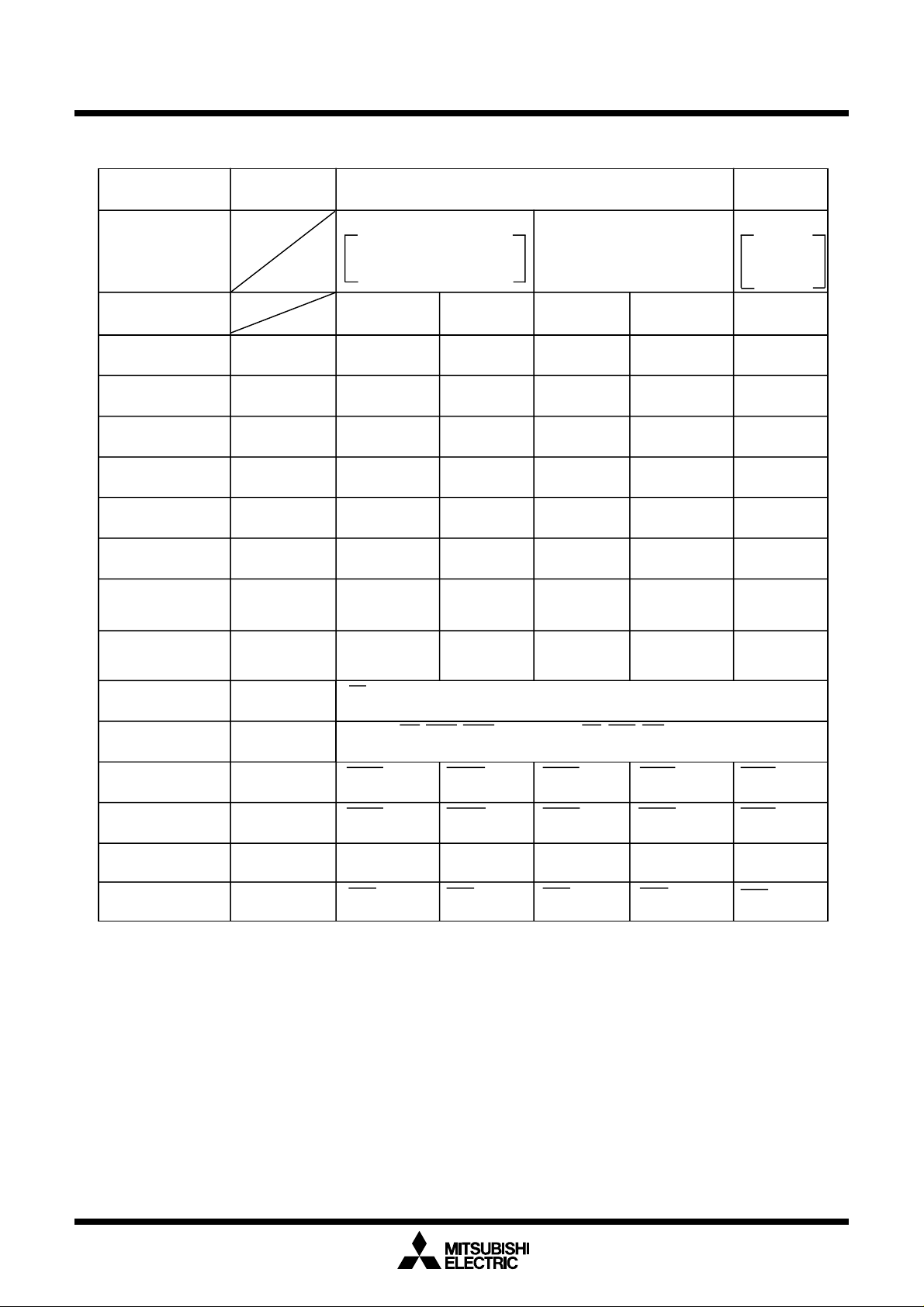
Mitsubishi microcomputers
M16C / 62A Group
SINGLE-CHIP 16-BIT CMOS MICROCOMPUTER
Bus Settings
Table 1.8.2. Pin functions for each processor mode
Processor mode
Multiplexed bus
space select bit
Data bus width
BYTE pin level
P00 to P0
P1
0
to P1
7
7
Single-chip
mode
I/O port Data bus Data bus Data bus Data bus I/O port
I/O port I/O port Data bus I/O port Data bus I/O port
Memory expansion mode/microprocessor modes
“01”, “10” “00”
Either CS1 or CS2 is for
multiplexed bus and others
are for separate bus
8 bits
“H”
16 bits
“L”
(separate bus)
8 bits
“H”
16 bits
“L”
Memory
expansion mode
“11” (Note 1)
multiplexed
bus for the
entire
space
8 bit
“H”
0
P2
P2
1
to P2
7
P3
0
P31 to P3
P4
Port P40 to P4
0
to P4
7
3
3
function select bit = 1
P4
0
to P4
Port P40 to P4
3
3
function select bit = 0
P4
4
to P4
7
P5
0
to P5
3
P5
4
P5
5
P5
6
I/O port
I/O port
I/O port
Address bus
/data bus
Address bus Address bus
/data bus
Address bus
(Note 2)
(Note 2)
Address bus Address bus Address bus Address bus
/data bus
(Note 2)
Address bus Address bus Address bus A8/D
/data bus
(Note 2)
/data bus
Address bus Address bus Address bus
/data bus
7
I/O port Address bus Address bus Address bus Address bus I/O port
I/O port I/O port I/O port /O port I/O port I/O port
I/O port Address bus Address bus Address bus Address bus I/O port
I/O port
CS (chip select) or programmable I/O port
(For details, refer to “Bus control”)
I/O port
Outputs RD, WRL, WRH, and BCLK or RD, BHE, WR, and BCLK
(For details, refer to “Bus control”)
I/O port HLDA HLDA HLDA HLDA HLDA
I/O port HOLD HOLD HOLD HOLD HOLD
I/O port ALE ALE ALE ALE ALE
P5
7
I/O port RDY RDY RDY RDY RDY
Note 1: If the entire space is of multiplexed bus in memory expansion mode, choose an 8-bit width.
The processor operates using the separate bus after reset is revoked, so the entire space multiplexed bus cannot be
chosen in microprocessor mode.
The higher-order address becomes a port if the entire space multiplexed bus is chosen, so only 256 bytes can be used
in each chip select.
Note 2: Address bus when in separate bus mode.
26
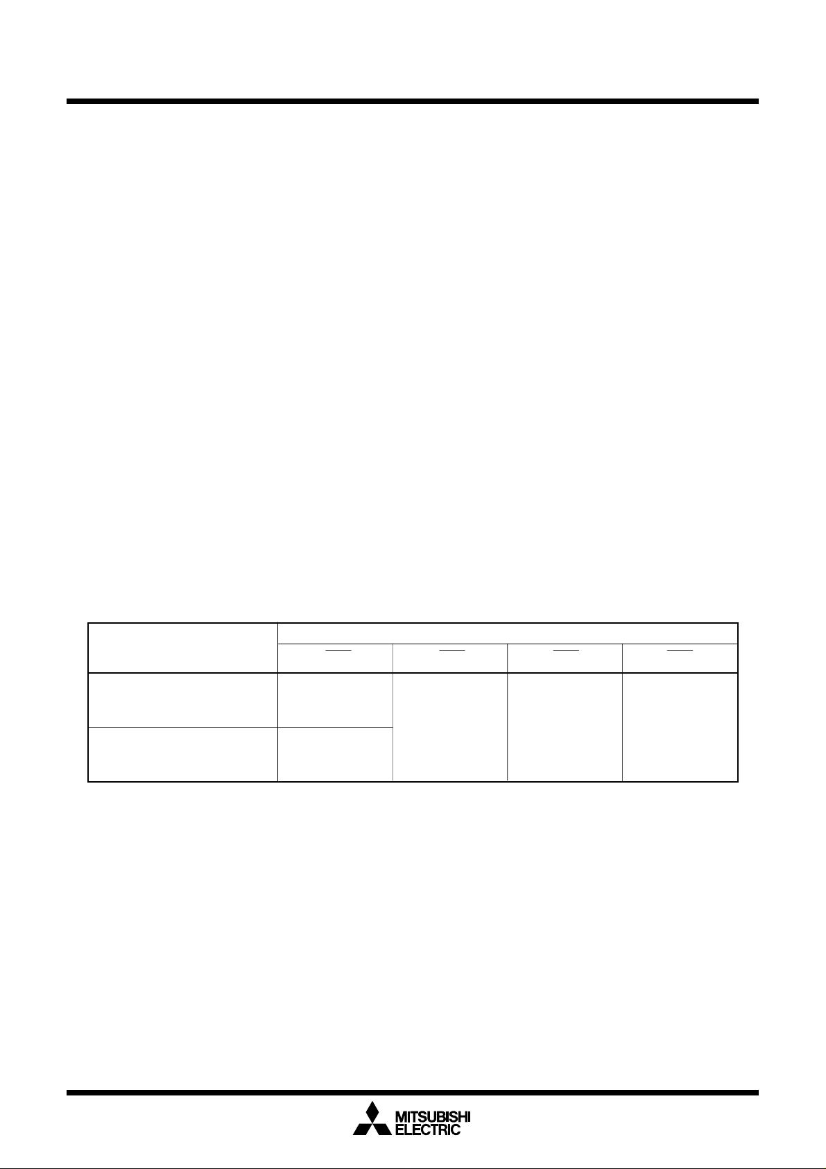
Mitsubishi microcomputer
s
p
R
M16C / 62A Grou
Bus Control
SINGLE-CHIP 16-BIT CMOS MICROCOMPUTE
Bus Control
The following explains the signals required for accessing external devices and software waits. The signals
required for accessing the external devices are valid when the processor mode is set to memory expansion
mode and microprocessor mode. The software waits are valid in all processor modes.
(1) Address bus/data bus
The address bus consists of the 20 pins A0 to A19 for accessing the 1M bytes of address space.
The data bus consists of the pins for data I/O. When the BYTE pin is “H”, the 8 ports D0 to D7 function
as the data bus. When BYTE is “L”, the 16 ports D0 to D15 function as the data bus.
When a change is made from single-chip mode to memory expansion mode, the value of the address
bus is undefined until external memory is accessed.
(2) Chip select signal
The chip select signal is output using the same pins as P44 to P47. Bits 0 to 3 of the chip select control
register (address 000816) set each pin to function as a port or to output the chip select signal. The chip
select control register is valid in memory expansion mode and microprocessor mode. In single-chip
mode, P44 to P47 function as programmable I/O ports regardless of the value in the chip select control
register.
In microprocessor mode, only CS0 outputs the chip select signal after the reset state has been can-
_______ _______
celled. CS1 to CS3 function as input ports. Figure 1.9.1 shows the chip select control register.
The chip select signal can be used to split the external area into as many as four blocks. Tables 1.9.1
and 1.9.2 show the external memory areas specified using the chip select signal.
_______
Table 1.9.1. External areas specified by the chip select signals
(A product having an internal RAM equal to or less than 15K bytes and a ROM equal to or less than 192K bytes)(Note)
Processor mode
Chip select signal
CS0 CS1 CS2 CS3
3000016 to
Memory expansion mode
Microprocessor mode
CFFFF
16
(640K bytes)
16 to
30000
FFFFF16
2800016 to
2FFFF
16
(32K bytes)
08000
16 to
27FFF
16
(128K bytes)
16 to
04000
07FFF
16
(16K bytes)
(832K bytes)
Note :Be sure to set bit 3 (PM13) of processor mode register 1 to “0”.
27
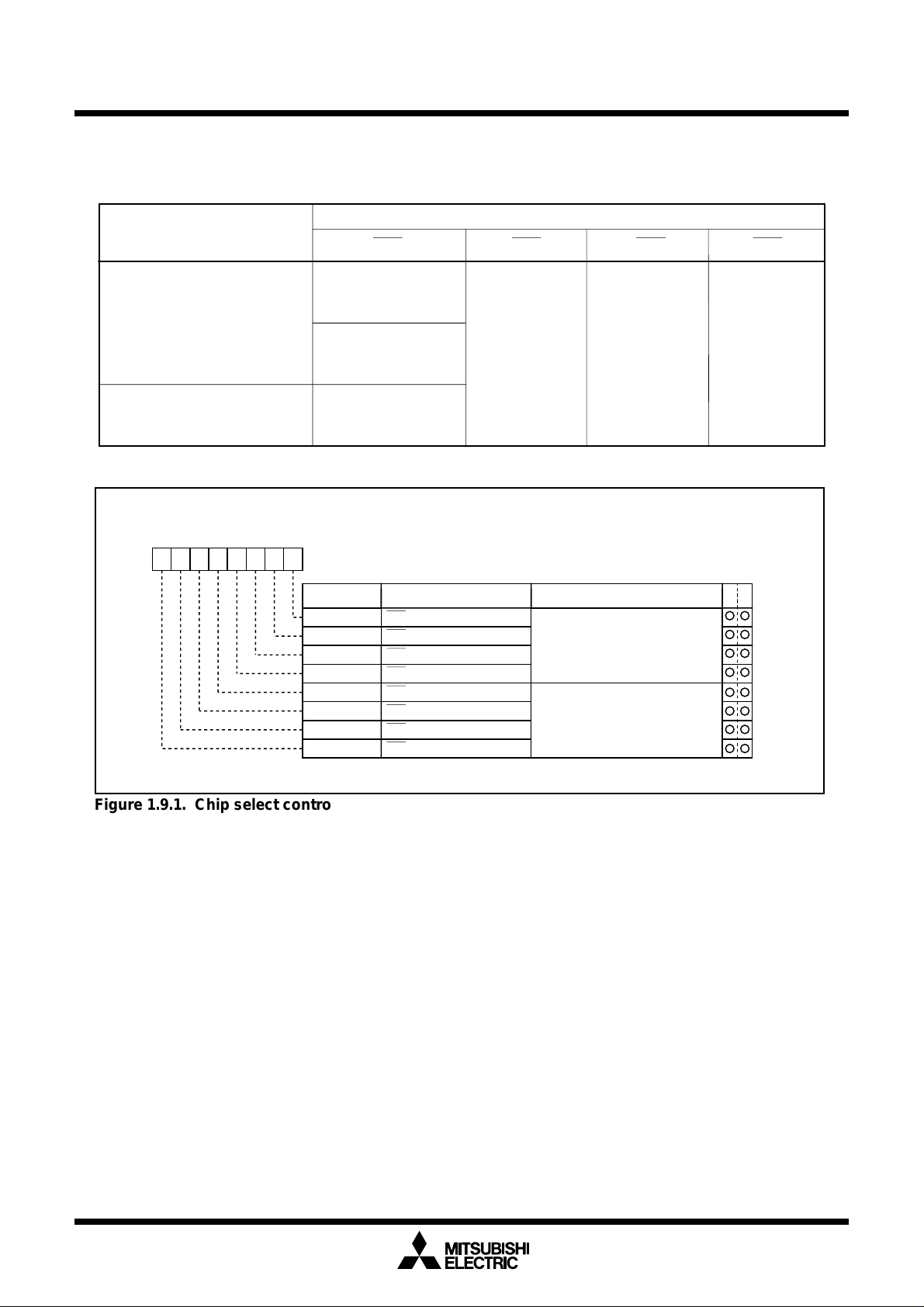
Mitsubishi microcomputers
M16C / 62A Group
SINGLE-CHIP 16-BIT CMOS MICROCOMPUTER
Bus Control
Table 1.9.2. External areas specified by the chip select signals
(A product having an internal RAM of more than 15K bytes and a ROM of more than 192K bytes)
Processor mode
Memory expansion mode
Microprocessor mode
Chip select control register
b7 b6 b5 b4 b3 b2 b1 b0
Chip select signal
CS0 CS1 CS2
When PM13=0
3000016 to CFFFF
(640K bytes)
When PM13=1
3000016 to BFFFF
(576K bytes)
03000
16
to FFFFF
(816K bytes)
Symbol Address When reset
CSR 0008
Bit symbol
CS0
CS1
CS2
CS3
CS0W
CS1W
CS2W
CS3W
CS0 output enable bit
CS1 output enable bit
CS2 output enable bit
CS3 output enable bit
CS0 wait bit
CS1 wait bit
CS2 wait bit
CS3 wait bit
16
16
16
Bit name
2800016 to
2FFFF
16
(32K bytes)
16
0 : Chip select output disabled
1 : Chip select output enabled
0 : Wait state inserted
1 : No wait state
01
16
(Normal port pin)
16
08000
27FFF
to
16
(128K bytes)
Function
CS3
When PM13=0
04000
16
to
07FFF
16
(16K bytes)
When PM13=1
16
06000
07FFF
to
16
(8K bytes)
W
R
Figure 1.9.1. Chip select control register
28
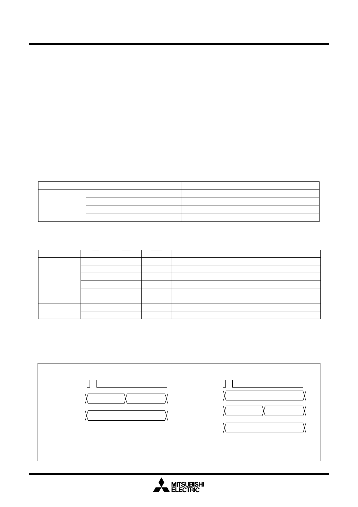
Mitsubishi microcomputer
s
p
R
M16C / 62A Grou
Bus Control
SINGLE-CHIP 16-BIT CMOS MICROCOMPUTE
(3) Read/write signals
With a 16-bit data bus (BYTE pin =“L”), bit 2 of the processor mode register 0 (address 000416) select the
combinations of RD, BHE, and WR signals or RD, WRL, and WRH signals. With an 8-bit data bus (BYTE
pin = “H”), use the combination of RD, WR, and BHE signals. (Set bit 2 of the processor mode register 0
(address 000416) to “0”.) Tables 1.9.3 and 1.9.4 show the operation of these signals.
After a reset has been cancelled, the combination of RD, WR, and BHE signals is automatically selected.
When switching to the RD, WRL, and WRH combination, do not write to external memory until bit 2 of the
processor mode register 0 (address 000416) has been set (Note).
Note: Before attempting to change the contents of the processor mode register 0, set bit 1 of the protect
register (address 000A16) to “1”.
_____ ________ ______ _____ ________ _________
_____ ______ _______
_____ ______ ________
_____ _________ _________
Table 1.9.3. Operation of RD, WRL, and WRH signals
_____ ________ _________
Data bus width
16-bit
(BYTE = “L”)
L
H
H
H
_____ ______ ________
H
L
H
L
WRHWRLRD
H
H
L
L
Read data
Write 1 byte of data to even address
Write 1 byte of data to odd address
Write data to both even and odd addresses
Status of external data bus
Table 1.9.4. Operation of RD, WR, and BHE signals
Data bus width A0
16-bit
(BYTE = “L”)
RD
BHEWR
HLL
LHL
HLH
LHH
H
H
HLLL
LHLL
8-bit
(BYTE = “H”)
HL H / L
LH H / L
Not used
Not used
Write 1 byte of data to odd address
Read 1 byte of data from odd address
L
L
Write 1 byte of data to even address
Read 1 byte of data from even address
Write data to both even and odd addresses
Read data from both even and odd addresses
Write 1 byte of data
Read 1 byte of data
Status of external data bus
(4) ALE signal
The ALE signal latches the address when accessing the multiplex bus space. Latch the address when the
ALE signal falls.
When BYTE pin = “H”
ALE
D
0/A0
to D7/A
A8 to A
7
19
Address Data (Note 1)
Address (Note 2)
Note 1: Floating when reading.
Note 2: When multiplexed bus for the entire space is selected, these are I/O ports.
Figure 1.9.2. ALE signal and address/data bus
When BYTE pin = “L”
ALE
0/A1
to D7/A
D
A9 to A
0
A
8
19
Address Data (Note 1)
Address
Address
29
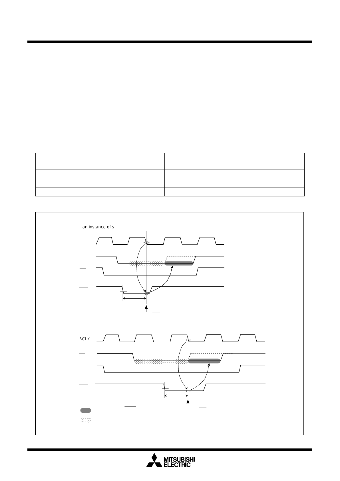
Mitsubishi microcomputers
M16C / 62A Group
SINGLE-CHIP 16-BIT CMOS MICROCOMPUTER
Bus Control
________
(5) The RDY signal
________
RDY is a signal that facilitates access to an external device that requires long access time. As shown in
Figure 1.9.3, if an “L” is being input to the RDY at the BCLK falling edge, the bus turns to the wait state. If
________
an “H” is being input to the RDY pin at the BCLK falling edge, the bus cancels the wait state. Table 1.9.5
shows the state of the microcomputer with the bus in the wait state, and Figure 1.9.3 shows an example
in which the RD signal is prolonged by the RDY signal.
________
____ ________
The RDY signal is valid when accessing the external area during the bus cycle in which bits 4 to 7 of the
chip select control register (address 000816) are set to “0”. The RDY signal is invalid when setting “1” to
all bits 4 to 7 of the chip select control register (address 000816), but the RDY pin should be treated as
properly as in non-using.
Table 1.9.5. Microcomputer status in ready state (Note)
Item Status
Oscillation On
___ _____
R/W signal, address bus, data bus, CS
__________
ALE signal, HLDA, programmable I/O ports
Internal peripheral circuits On
________
Note: The RDY signal cannot be received immediately prior to a software wait.
________
________
________
________
Maintain status when RDY signal received
In an instance of separate bus
BCLK
RD
CS
i
(i=0 to 3)
RDY
Accept timing of RDY signal
In an instance of multiplexed bus
BCLK
RD
CS
i
(i=0 to 3)
RDY
tsu(RDY - BCLK)
tsu(RDY - BCLK)
: Wait using RDY signal
: Wait using software
Figure 1.9.3. Example of RD signal extended by RDY signal
30
Accept timing of RDY signal
_____ ________

Mitsubishi microcomputer
s
p
R
M16C / 62A Grou
Bus Control
SINGLE-CHIP 16-BIT CMOS MICROCOMPUTE
(6) Hold signal
The hold signal is used to transfer the bus privileges from the CPU to the external circuits. Inputting “L” to
__________
the HOLD pin places the microcomputer in the hold state at the end of the current bus access. This status
__________ __________
is maintained and “L” is output from the HLDA pin as long as “L” is input to the HOLD pin. Table 1.9.6
shows the microcomputer status in the hold state.
__________
Bus-using priorities are given to HOLD, DMAC, and CPU in order of decreasing precedence.
__________
HOLD > DMAC > CPU
Figure 1.9.4. Bus-using priorities
Table 1.9.6. Microcomputer status in hold state
Item Status
Oscillation ON
___ _____ _______
R/W signal, address bus, data bus, CS, BHE Floating
Programmable I/O ports P0, P1, P2, P3, P4, P5 Floating
__________
HLDA Output “L”
Internal peripheral circuits ON (but watchdog timer stops)
ALE signal Undefined
P6, P7, P8, P9, P10 Maintains status when hold signal is received
(7) External bus status when the internal area is accessed
Table 1.9.7 shows the external bus status when the internal area is accessed.
Table 1.9.7. External bus status when the internal area is accessed
Item SFR accessed Internal ROM/RAM accessed
Address bus Address output Maintain status before accessed
address of external area
Data bus When read Floating Floating
When write Output data Undefined
RD, WR, WRL, WRH RD, WR, WRL, WRH output Output “H”
BHE BHE output Maintain status before accessed
status of external area
CS Output “H” Output “H”
ALE Output “L” Output “L”
31

Mitsubishi microcomputers
M16C / 62A Group
SINGLE-CHIP 16-BIT CMOS MICROCOMPUTER
Bus Control
(8) BCLK output
The user can choose the BCLK output by use of bit 7 of processor mode register 0 (000416) (Note).
When set to “1”, the output floating.
Note: Before attempting to change the contents of the processor mode register 0, set bit 1 of the protect
register (address 000A16) to “1”.
(9) Software wait
A software wait can be inserted by setting the wait bit (bit 7) of the processor mode register 1 (address
000516) (Note) and bits 4 to 7 of the chip select control register (address 000816).
A software wait is inserted in the internal ROM/RAM area and in the external memory area by setting the
wait bit of the processor mode register 1. When set to “0”, each bus cycle is executed in one BCLK cycle.
When set to “1”, each bus cycle is executed in two or three BCLK cycles. After the microcomputer has been
reset, this bit defaults to “0”. When
cycles), regardless of the contents of bits 4 to 7 of the chip select control register
to the recommended operating conditions (main clock input oscillation frequency) of the electric characteristics.
However, when the user is using the RDY signal, the relevant bit in the chip select control register’s
bits 4 to 7 must be set to “0”.
When the wait bit of the processor mode register 1 is “0”, software waits can be set independently for
each of the 4 areas selected using the chip select signal. Bits 4 to 7 of the chip select control register
_______ _______
correspond to chip selects CS0 to CS3. When one of these bits is set to “1”, the bus cycle is executed in
one BCLK cycle. When set to “0”, the bus cycle is executed in two or three BCLK cycles. These bits
default to “0” after the microcomputer has been reset.
The SFR area is always accessed in two BCLK cycles regardless of the setting of these control bits. Also,
insert a software wait if using the multiplex bus to access the external memory area.
Table 1.9.8 shows the software wait and bus cycles. Figure 1.9.5 shows example bus timing when using
software waits.
Note: Before attempting to change the contents of the processor mode register 1, set bit 1 of the protect
register (address 000A16) to “1”.
set to “1”, a wait is applied to all memory areas (two or three BCLK
. Set this bit after referring
________
Table 1.9.8. Software waits and bus cycles
Area Bus status Wait bit
SFR
Internal
ROM/RAM
Separate bus
External
memory
area
Note: When using the RDY signal, always set to “0”.
32
Separate bus
Separate bus
Multiplex bus 0 0 3 BCLK cycles
Multiplex bus
Bits 4 to 7 of chip select
control register
Invalid Invalid 2 BCLK cycles
0 Invalid 1 BCLK cycle
Invalid1 2 BCLK cycles
0 1 1 BCLK cycle
0 0 2 BCLK cycles
1 0 (Note) 2 BCLK cycles
1 3 BCLK cycles0 (Note)
Bus cycle

s
p
R
Bus Control
Mitsubishi microcomputer
M16C / 62A Grou
SINGLE-CHIP 16-BIT CMOS MICROCOMPUTE
< Separate bus (no wait) >
BCLK
Write signal
Read signal
Data bus
Address bus (Note 2)
Chip select (Note 2)
< Separate bus (with wait) >
BCLK
Write signal
Read signal
Bus cycle (Note 1)
Output
Address
Bus cycle (Note 1) Bus cycle (Note 1)
Bus cycle (Note 1)
Input
Address
Data bus
Address bus (Note 2)
Chip select (Note 2)
< Multiplexed bus >
Write signal
Read signal
Address bus (Note 2)
Address bus/
Data bus
Chip select (Note 2)
BCLK
ALE
Output
Address
Bus cycle (Note 1) Bus cycle (Note 1)
Address
Address
Address
Data output
Address
Input
Address
Input
Note 1: These example timing charts indicate bus cycle length.
After this bus cycle sometimes come read and write cycles in succession.
Note 2: The address bus and chip select may be extended depending on the CPU status
such as that of the instruction queue buffer.
Figure 1.9.5. Typical bus timings using software wait
33

Mitsubishi microcomputer
s
p
R
M16C / 62A Grou
Clock Generating Circuit
SINGLE-CHIP 16-BIT CMOS MICROCOMPUTE
Clock Generating Circuit
The clock generating circuit contains two oscillator circuits that supply the operating clock sources to the
CPU and internal peripheral units.
Table 1.10.1. Main clock and sub-clock generating circuits
Main clock generating circuit Sub-clock generating circuit
Use of clock • CPU’s operating clock source • CPU’s operating clock source
• Internal peripheral units’ • Timer A/B’s count clock
operating clock source source
Usable oscillator Ceramic or crystal oscillator Crystal oscillator
Pins to connect oscillator XIN, XOUT XCIN, XCOUT
Oscillation stop/restart function Available Available
Oscillator status immediately after reset
Other Externally derived clock can be input
Oscillating Stopped
Example of oscillator circuit
Figure 1.10.1 shows some examples of the main clock circuit, one using an oscillator connected to the
circuit, and the other one using an externally derived clock for input. Figure 1.10.2 shows some examples
of sub-clock circuits, one using an oscillator connected to the circuit, and the other one using an externally
derived clock for input. Circuit constants in Figures 1.10.1 and 1.10.2 vary with each oscillator used. Use
the values recommended by the manufacturer of your oscillator.
Microcomputer
(Built-in feedback resistor)
X
IN
C
IN
Note: Insert a damping resistor if required. The resistance will vary depending on the oscillator and the oscillation drive
capacity setting. Use the value recommended by the maker of the oscillator.
When the oscillation drive capacity is set to low, check that oscillation is stable. Also, if the oscillator manufacturer's
data sheet specifies that a feedback resistor be added external to the chip, insert a feedback resistor between X
and X
OUT
X
OUT
(Note)
R
d
C
OUT
following the instruction.
Figure 1.10.1. Examples of main clock
Microcomputer
(Built-in feedback resistor)
X
IN
Externally derived clock
Vcc
Vss
X
OUT
Open
IN
Microcomputer
(Built-in feedback resistor)
X
CIN
C
CIN
Note: Insert a damping resistor if required. The resistance will vary depending on the oscillator and the oscillation drive
capacity setting. Use the value recommended by the maker of the oscillator.
When the oscillation drive capacity is set to low, check that oscillation is stable. Also, if the oscillator manufacturer's
data sheet specifies that a feedback resistor be added external to the chip, insert a feedback resistor between X
COUT
and X
X
COUT
(Note)
R
C
following the instruction.
Figure 1.10.2. Examples of sub-clock
34
Cd
COUT
Microcomputer
(Built-in feedback resistor)
X
CIN
Externally derived clock
Vcc
Vss
X
COUT
Open
CIN

s
p
R
Clock Generating Circuit
Clock Control
Figure 1.10.3 shows the block diagram of the clock generating circuit.
X
CIN
X
COUT
CM04
Sub clock
RESET
Software reset
NMI
Interrupt request
level judgment
output
CM10 “1”
Write signal
WAIT instruction
Q
S
R
QS
R
CM05
X
IN
Main clock
X
OUT
CM02
Mitsubishi microcomputer
M16C / 62A Grou
SINGLE-CHIP 16-BIT CMOS MICROCOMPUTE
C32
f
1/32
f
C
f
1
f
AD
f
8
f
32
c
b
a
Divider
d
f
C
CM07=0
CM07=1
f1SIO2
f8SIO2
f32SIO2
BCLK
CM0i : Bit i at address 0006
CM1i : Bit i at address 0007
WDCi : Bit i at address 000F
16
16
16
Figure 1.10.3. Clock generating circuit
a
b
1/2 1/2 1/2 1/2
CM06=1
CM06=0
CM17,CM16=01
CM06=0
CM17,CM16=00
CM06=0
CM17,CM16=10
1/2
CM06=0
CM17,CM16=11
Details of divider
c
d
35

Mitsubishi microcomputer
s
p
R
M16C / 62A Grou
Clock Generating Circuit
The following paragraphs describes the clocks generated by the clock generating circuit.
SINGLE-CHIP 16-BIT CMOS MICROCOMPUTE
(1) Main clock
The main clock is generated by the main clock oscillation circuit. After a reset, the clock is divided by 8 to
the BCLK. The clock can be stopped using the main clock stop bit (bit 5 at address 000616). Stopping the
clock, after switching the operating clock source of CPU to the sub-clock, reduces the power dissipation.
After the oscillation of the main clock oscillation circuit has stabilized, the drive capacity of the main clock
oscillation circuit can be reduced using the XIN-XOUT drive capacity select bit (bit 5 at address 000716).
Reducing the drive capacity of the main clock oscillation circuit reduces the power dissipation. This bit
changes to “1” when shifting from high-speed/medium-speed mode to stop mode and at a reset. When
shifting from low-speed/low power dissipation mode to stop mode, the value before stop mode is retained.
(2) Sub-clock
The sub-clock is generated by the sub-clock oscillation circuit. No sub-clock is generated after a reset.
After oscillation is started using the port Xc select bit (bit 4 at address 000616), the sub-clock can be
selected as the BCLK by using the system clock select bit (bit 7 at address 000616). However, be sure
that the sub-clock oscillation has fully stabilized before switching.
After the oscillation of the sub-clock oscillation circuit has stabilized, the drive capacity of the sub-clock
oscillation circuit can be reduced using the XCIN-XCOUT drive capacity select bit (bit 3 at address 000616).
Reducing the drive capacity of the sub-clock oscillation circuit reduces the power dissipation. This bit
changes to “1” when shifting to stop mode and at a reset.
(3) BCLK
The BCLK is the clock that drives the CPU, and is fc or the clock is derived by dividing the main clock by
1, 2, 4, 8, or 16. The BCLK is derived by dividing the main clock by 8 after a reset. The BCLK signal can
be output from BCLK pin by the BCLK output disable bit (bit 7 at address 000416) in the memory expansion and the microprocessor modes.
The main clock division select bit 0(bit 6 at address 000616) changes to “1” when shifting from highspeed/medium-speed to stop mode and at reset. When shifting from low-speed/low power dissipation
mode to stop mode, the value before stop mode is retained.
(4) Peripheral function clock(f1, f8, f32, f1SIO2, f8SIO2,f32SIO2,fAD)
The clock for the peripheral devices is derived from the main clock or by dividing it by 1, 8, or 32. The
peripheral function clock is stopped by stopping the main clock or by setting the WAIT peripheral function
clock stop bit (bit 2 at 000616) to “1” and then executing a WAIT instruction.
(5) fC32
This clock is derived by dividing the sub-clock by 32. It is used for the timer A and timer B counts.
(6) fC
This clock has the same frequency as the sub-clock. It is used for the BCLK and for the watchdog timer.
36

s
p
R
Clock Generating Circuit
Figure 1.10.4 shows the system clock control registers 0 and 1.
System clock control register 0 (Note 1)
b7 b6 b5 b4 b3 b2 b1 b0
Symbol Address When reset
CM0 0006
16
48
Mitsubishi microcomputer
M16C / 62A Grou
SINGLE-CHIP 16-BIT CMOS MICROCOMPUTE
16
CM00
CM01
CM02
CM03
CM04
CM05
CM06
CM07
Bit name FunctionBit symbol
Clock output function
select bit
(Valid only in single-chip
mode)
WAIT peripheral function
clock stop bit
X
CIN-XCOUT
select bit (Note 2)
Port XC select bit 0 : I/O port
Main clock (XIN-X
stop bit (Note 3, 4, 5)
Main clock division select
bit 0 (Note 7)
System clock select bit
(Note 6)
drive capacity
OUT
b1 b0
0 0 : I/O port P5
0 1 : fC output
1 0 : f
8
output
1 1 : f
32
output
0 : Do not stop peripheral function clock in wait mode
1 : Stop peripheral function clock in wait mode (Note 8)
0 : LOW
1 : HIGH
1 : X
CIN-XCOUT
)
0 : On
1 : Off
0 : CM16 and CM17 valid
1 : Division by 8 mode
0 : XIN, X
1 : X
CIN
, X
OUT
COUT
7
generation
WR
Note 1: Set bit 0 of the protect register (address 000A16) to “1” before writing to this register.
Note 2: Changes to “1” when shiffing to stop mode and at a reset.
Note 3: When entering power saving mode, main clock stops using this bit. When returning from stop mode and
operating with X
IN
, set this bit to “0”. When main clock oscillation is operating by itself, set system clock select
bit (CM07) to “1” before setting this bit to “1”.
Note 4: When inputting external clock, only clock oscillation buffer is stopped and clock input is acceptable.
Note 5: If this bit is set to “1”, X
pulled up to X
OUT
OUT
turns “H”. The built-in feedback resistor remains being connected, so XIN turns
(“H”) via the feedback resistor.
Note 6: Set port Xc select bit (CM04) to “1” and stabilize the sub-clock oscillating before setting to this bit from “0” to “1”.
Do not write to both bits at the same time. And also, set the main clock stop bit (CM05) to “0” and stabilize the
main clock oscillating before setting this bit from “1” to “0”.
Note 7: This bit changes to “1” when shifting from high-speed/medium-speed mode to stop mode and at a reset. When
shifting from low-speed/low power dissipation mode to stop mode, the value before stop mode is retained.
Note 8: f
C32
is not included.
System clock control register 1 (Note 1)
b7 b6 b5 b4 b3 b2 b1 b0
00
00
Note 1: Set bit 0 of the protect register (address 000A16) to “1” before writing to this register.
Note 2: This bit changes to “1” when shifting from high-speed/medium-speed mode to stop mode and at a reset. When
shifting from low-speed/low power dissipation mode to stop mode, the value before stop mode is retained.
Note 3: Can be selected when bit 6 of the system clock control register 0 (address 0006
fixed at 8.
Note 4: If this bit is set to “1”, X
impedance state.
Symbol Address When reset
CM1 0007
16
20
16
Bit name FunctionBit symbol
CM10
Reserved bit
Reserved bit
Reserved bit
Reserved bit
CM15
CM16
CM17
All clock stop control bit
(Note4)
X
IN-XOUT
drive capacity
select bit (Note 2)
Main clock division
select bit 1 (Note 3)
OUT
turns “H”, and the built-in feedback resistor is cut off. X
0 : Clock on
1 : All clocks off (stop mode)
Always set to
Always set to
Always set to
Always set to
0 : LOW
1 : HIGH
b7 b6
0 0 : No division mode
0 1 : Division by 2 mode
1 0 : Division by 4 mode
1 1 : Division by 16 mode
“0”
“0”
“0”
“0”
16
) is “0”. If “1”, division mode is
CIN
and X
COUT
turn high-
WR
Figure 1.10.4. Clock control registers 0 and 1
37

Mitsubishi microcomputer
s
p
R
M16C / 62A Grou
Clock Generating Circuit
SINGLE-CHIP 16-BIT CMOS MICROCOMPUTE
Clock Output
In single-chip mode, the clock output function select bits (bits 0 and 1 at address 000616) enable f8, f32, or
fc to be output from the P57/CLKOUT pin. When the WAIT peripheral function clock stop bit (bit 2 at address
000616) is set to “1”, the output of f8 and f32 stops when a WAIT instruction is executed.
Stop Mode
Writing “1” to the all-clock stop control bit (bit 0 at address 000716) stops all oscillation and the microcomputer enters stop mode. In stop mode, the content of the internal RAM is retained provided that VCC remains above 2V.
Because the oscillation , BCLK, f1 to f32, f1SIO2 to f32SIO2, fC, fC32, and fAD stops in stop mode, peripheral
functions such as the A-D converter and watchdog timer do not function. However, timer A and timer B
operate provided that the event counter mode is set to an external pulse, and UARTi(i = 0 to 2), SI/O3,4
functions provided an external clock is selected. Table 1.10.2 shows the status of the ports in stop mode.
Stop mode is cancelled by a hardware reset or an interrupt. If an interrupt is to be used to cancel stop mode,
that interrupt must first have been enabled. If returning by an interrupt, that interrupt routine is executed.
When shifting from high-speed/medium-speed mode to stop mode and at a reset, the main clock division
select bit 0 (bit 6 at address 000616) is set to “1”. When shifting from low-speed/low power dissipation mode
to stop mode, the value before stop mode is retained.
Table 1.10.2. Port status during stop mode
Pin Memory expansion mode Single-chip mode
Microprocessor mode
Address bus, data bus, CS0 to CS3
_____ ______ ________ ________ _________
_______ _______
Retains status before stop mode
RD, WR, BHE, WRL, WRH “H”
__________
HLDA, BCLK “H”
ALE “H”
Port
Retains status before stop mode
CLKOUT When fc selected Valid only in single-chip mode “H”
When f8, f32 selected Valid only in single-chip mode
Retains status before stop mode
Retains status before stop mode
38

Mitsubishi microcomputer
s
p
R
M16C / 62A Grou
Wait Mode
SINGLE-CHIP 16-BIT CMOS MICROCOMPUTE
Wait Mode
When a WAIT instruction is executed, the BCLK stops and the microcomputer enters the wait mode. In this
mode, oscillation continues but the BCLK and watchdog timer stop. Writing “1” to the WAIT peripheral
function clock stop bit and executing a WAIT instruction stops the clock being supplied to the internal
peripheral functions, allowing power dissipation to be reduced. Table 1.10.3 shows the status of the ports in
wait mode.
Wait mode is cancelled by a hardware reset or an interrupt. If an interrupt is used to cancel wait mode, the
microcomputer restarts from the interrupt routine using as BCLK, the clock that had been selected when the
WAIT instruction was executed.
Table 1.10.3. Port status during wait mode
Pin Memory expansion mode Single-chip mode
Address bus, data bus, CS0 to CS3
_______ _______
_____ ______ ________ ________ _________
RD, WR, BHE, WRL, WRH “H”
__________
HLDA,BCLK “H”
ALE “H”
Port
CLKOUT When fC selected Valid only in single-chip mode Does not stop
When f8, f32 selected Valid only in single-chip mode Does not stop when the WAIT
Microprocessor mode
Retains status before wait mode
Retains status before wait mode Retains status before wait mode
peripheral function clock stop
bit is “0”.
When the WAIT peripheral
function clock stop bit is “1”,
the status immediately prior
to entering wait mode is maintained.
39

Mitsubishi microcomputer
s
p
R
M16C / 62A Grou
Status Transition Of BCLK
SINGLE-CHIP 16-BIT CMOS MICROCOMPUTE
Status Transition Of BCLK
Power dissipation can be reduced and low-voltage operation achieved by changing the count source for
BCLK. Table 1.10.4 shows the operating modes corresponding to the settings of system clock control
registers 0 and 1.
When reset, the device starts in division by 8 mode. The main clock division select bit 0(bit 6 at address
000616) changes to “1” when shifting from high-speed/medium-speed to stop mode and at a reset. When
shifting from low-speed/low power dissipation mode to stop mode, the value before stop mode is retained.
The following shows the operational modes of BCLK.
(1) Division by 2 mode
The main clock is divided by 2 to obtain the BCLK.
(2) Division by 4 mode
The main clock is divided by 4 to obtain the BCLK.
(3) Division by 8 mode
The main clock is divided by 8 to obtain the BCLK. When reset, the device starts operating from this
mode. Before the user can go from this mode to no division mode, division by 2 mode, or division by 4
mode, the main clock must be oscillating stably. When going to low-speed or lower power consumption
mode, make sure the sub-clock is oscillating stably.
(4) Division by 16 mode
The main clock is divided by 16 to obtain the BCLK.
(5) No-division mode
The main clock is divided by 1 to obtain the BCLK.
(6) Low-speed mode
fC is used as the BCLK. Note that oscillation of both the main and sub-clocks must have stabilized before
transferring from this mode to another or vice versa. At least 2 to 3 seconds are required after the subclock starts. Therefore, the program must be written to wait until this clock has stabilized immediately
after powering up and after stop mode is cancelled.
(7) Low power dissipation mode
fC is the BCLK and the main clock is stopped.
Note : Before the count source for BCLK can be changed from XIN to XCIN or vice versa, the clock to which
the count source is going to be switched must be oscillating stably. Allow a wait time in software for
the oscillation to stabilize before switching over the clock.
Table 1.10.4. Operating modes dictated by settings of system clock control registers 0 and 1
CM17 CM16 CM07 CM06 CM05 CM04
01000Invalid Division by 2 mode
10000Invalid Division by 4 mode
Invalid Invalid 0 1 0 Invalid Division by 8 mode
11000Invalid Division by 16 mode
00000Invalid No-division mode
Invalid Invalid 1 Invalid 0 1 Low-speed mode
Invalid Invalid 1 Invalid 1 1 Low power dissipation mode
Operating mode of BCLK
40

s
p
R
Power control
Power control
The following is a description of the three available power control modes:
Modes
Power control is available in three modes.
(a) Normal operation mode
• High-speed mode
Divide-by-1 frequency of the main clock becomes the BCLK. The CPU operates with the internal
clock selected. Each peripheral function operates according to its assigned clock.
• Medium-speed mode
Divide-by-2, divide-by-4, divide-by-8, or divide-by-16 frequency of the main clock becomes the
BCLK. The CPU operates according to the internal clock selected. Each peripheral function operates according to its assigned clock.
Mitsubishi microcomputer
M16C / 62A Grou
SINGLE-CHIP 16-BIT CMOS MICROCOMPUTE
• Low-speed mode
fC becomes the BCLK. The CPU operates according to the fc clock. The fc clock is supplied by the
secondary clock. Each peripheral function operates according to its assigned clock.
• Low power consumption mode
The main clock operating in low-speed mode is stopped. The CPU operates according to the fC
clock. The fc clock is supplied by the secondary clock. The only peripheral functions that operate
are those with the sub-clock selected as the count source.
(b) Wait mode
The CPU operation is stopped. The oscillators do not stop.
(c) Stop mode
All oscillators stop. The CPU and all built-in peripheral functions stop. This mode, among the three
modes listed here, is the most effective in decreasing power consumption.
Figure 1.10.5 is the state transition diagram of the above modes.
41

s
p
R
Power control
Transition of stop mode, wait mode
Mitsubishi microcomputer
M16C / 62A Grou
SINGLE-CHIP 16-BIT CMOS MICROCOMPUTE
Reset
All oscillators stopped
Stop mode
All oscillators stopped
Stop mode
All oscillators stopped
Stop mode
CM10 = “1”
Interrupt
Interrupt
CM10 = “1”
CM10 = “1”
Interrupt
Transition of normal mode
Main clock is oscillating
Sub clock is stopped
Medium-speed mode
(divided-by-8 mode)
CM06 = “1”
Main clock is oscillating
Sub clock is oscillating
High-speed mode
BCLK : f(XIN)
CM07 = “0” CM06 = “0”
CM17 = “0” CM16 = “0”
Medium-speed mode
(divided-by-4 mode)
BCLK : f(XIN)/4
CM07 = “0” CM06 = “0”
CM17 = “1” CM16 = “0”
CM07 = “0” CM06 = “1”
CM04 = “0”
Medium-speed mode
(divided-by-2 mode)
CM07 = “0” CM06 = “0”
CM17 = “0” CM16 = “1”
Medium-speed mode
(divided-by-16 mode)
CM07 = “0” CM06 = “0”
CM17 = “1” CM16 = “1”
BCLK : f(XIN)/8
CM04 = “1”
(Notes 1, 3)
BCLK : f(XIN)/2
BCLK : f(XIN)/16
CPU operation stopped
Wait mode
CPU operation stopped
Wait mode
CPU operation stopped
Wait mode
Medium-speed mode
(divided-by-8 mode)
High-speed/medium-
speed mode
Low-speed/low power
dissipation mode
WAIT
instruction
Interrupt
WAIT
instruction
Interrupt
WAIT
instruction
Interrupt
Normal mode
(Refer to the following for the transition of normal mode.)
CM07 = “0” (Note 1)
CM06 = “1”
CM04 = “0”
Main clock is oscillating
Medium-speed mode
(divided-by-8 mode)
BCLK : f(XIN)/8
CM07 = “0”
CM06 = “1”
CM07 = “0”
(Note 1, 3)
CM07 = “1”
(Note 2)
Sub clock is oscillating
Low-speed mode
BCLK : f(X
CM05 = “0” CM05 = “1”
CIN
CM07 = “1”
)
CM04 = “0” CM04 = “1”
Main clock is oscillating
Sub clock is stopped
Medium-speed mode
CM06 = “0”
(Notes 1,3)
High-speed mode
BCLK : f(XIN)
CM07 = “0” CM06 = “0”
CM17 = “0” CM16 = “0”
Medium-speed mode
(divided-by-4 mode)
BCLK : f(XIN)/4
CM07 = “0” CM06 = “0”
CM17 = “1” CM16 = “0”
(divided-by-2 mode)
BCLK : f(XIN)/2
CM07 = “0” CM06 = “0”
CM17 = “0” CM16 = “1”
Medium-speed mode
(divided-by-16 mode)
BCLK : f(XIN)/16
CM07 = “0” CM06 = “0”
CM17 = “1” CM16 = “1”
Note 1: Switch clock after oscillation of main clock is sufficiently stable.
Note 2: Switch clock after oscillation of sub clock is sufficiently stable.
Note 3: Change CM06 after changing CM17 and CM16.
Note 4: Transit in accordance with arrow.
Figure 1.10.5. State transition diagram of Power control mode
42
CM07 = “1” (Note 2)
CM05 = “1”
CM07 = “0” (Note 1)
CM06 = “0” (Note 3)
CM04 = “1”
Main clock is stopped
Sub clock is oscillating
Low power dissipation mode
BCLK : f(X
CIN
CM07 = “1”
)

Mitsubishi microcomputer
s
p
R
A
M16C / 62A Grou
Protection
SINGLE-CHIP 16-BIT CMOS MICROCOMPUTE
Protection
The protection function is provided so that the values in important registers cannot be changed in the event
that the program runs out of control. Figure 1.10.6 shows the protect register. The values in the processor
mode register 0 (address 000416), processor mode register 1 (address 000516), system clock control register 0 (address 000616), system clock control register 1 (address 000716), port P9 direction register (address 03F316) , SI/O3 control register (address 036216) and SI/O4 control register (address 036616) can
only be changed when the respective bit in the protect register is set to “1”. Therefore, important outputs
can be allocated to port P9.
If, after “1” (write-enabled) has been written to the port P9 direction register and SI/Oi control register
(i=3,4) write-enable bit (bit 2 at address 000A16), a value is written to any address, the bit automatically
reverts to “0” (write-inhibited). However, the system clock control registers 0 and 1 write-enable bit (bit 0 at
000A16) and processor mode register 0 and 1 write-enable bit (bit 1 at 000A16) do not automatically return
to “0” after a value has been written to an address. The program must therefore be written to return these
bits to “0”.
Protect register
b7 b6 b5 b4 b3 b2 b1 b0
Nothing is assigned.
In an attempt to write to these bits, write “0”. The value, if read, turns out to be
indeterminate.
Note: Writing a value to an address after “1” is written to this bit returns the bit
Figure 1.10.6. Protect register
Symbol Address When reset
PRCR 000A
PRC0
PRC1
PRC2
Enables writing to system clock
control registers 0 and 1 (addresses
0006
16
and 0007
Enables writing to processor mode
registers 0 and 1 (addresses 0004
and 0005
Enables writing to port P9 direction
register (address 03F3
control register (i=3,4) (addresses
0362
16
16
and 036616) (Note
16
XXXXX000
Bit nameBit symbol
16
)
)
16
) and SI/Oi
2
0 : Write-inhibited
1 : Write-enabled
0 : Write-inhibited
16
1 : Write-enabled
0 : Write-inhibited
1 : Write-enabled
Function
)
to “0” . Other bits do not automatically return to “0” and they must therefore
be reset by the program.
WR
43

s
p
R
Interrupt
Overview of Interrupt
Type of Interrupts
Figure 1.11.1 lists the types of interrupts.
Software
Interrupt
Hardware
Special
Peripheral I/O (Note)
Mitsubishi microcomputer
M16C / 62A Grou
SINGLE-CHIP 16-BIT CMOS MICROCOMPUTE
Undefined instruction (UND instruction)
Overflow (INTO instruction)
BRK instruction
INT instruction
Reset
_______
NMI
________
DBC
Watchdog timer
Single step
Address matched
Note: Peripheral I/O interrupts are generated by the peripheral functions built into the microcomputer system.
Figure 1.11.1. Classification of interrupts
• Maskable interrupt : An interrupt which can be enabled (disabled) by the interrupt enable flag
(I flag) or whose interrupt priority can be changed by priority level.
• Non-maskable interrupt : An interrupt which cannot be enabled (disabled) by the interrupt enable flag
(I flag) or whose interrupt priority cannot be changed by priority level.
44

Mitsubishi microcomputer
s
p
R
M16C / 62A Grou
Interrupt
SINGLE-CHIP 16-BIT CMOS MICROCOMPUTE
Software Interrupts
A software interrupt occurs when executing certain instructions. Software interrupts are non-maskable
interrupts.
• Undefined instruction interrupt
An undefined instruction interrupt occurs when executing the UND instruction.
• Overflow interrupt
An overflow interrupt occurs when executing the INTO instruction with the overflow flag (O flag) set to
“1”. The following are instructions whose O flag changes by arithmetic:
ABS, ADC, ADCF, ADD, CMP, DIV, DIVU, DIVX, NEG, RMPA, SBB, SHA, SUB
• BRK interrupt
A BRK interrupt occurs when executing the BRK instruction.
• INT interrupt
An INT interrupt occurs when specifying one of software interrupt numbers 0 through 63 and executing the INT instruction. Software interrupt numbers 0 through 31 are assigned to peripheral I/O interrupts, so executing the INT instruction allows executing the same interrupt routine that a peripheral I/
O interrupt does.
The stack pointer (SP) used for the INT interrupt is dependent on which software interrupt number is
involved.
So far as software interrupt numbers 0 through 31 are concerned, the microcomputer saves the stack
pointer assignment flag (U flag) when it accepts an interrupt request. If change the U flag to “0” and
select the interrupt stack pointer (ISP), and then execute an interrupt sequence. When returning from
the interrupt routine, the U flag is returned to the state it was before the acceptance of interrupt request. So far as software numbers 32 through 63 are concerned, the stack pointer does not make a
shift.
45

s
p
R
Interrupt
SINGLE-CHIP 16-BIT CMOS MICROCOMPUTE
Hardware Interrupts
Hardware interrupts are classified into two types — special interrupts and peripheral I/O interrupts.
(1) Special interrupts
Special interrupts are non-maskable interrupts.
M16C / 62A Grou
• Reset
Reset occurs if an “L” is input to the RESET pin.
_______
• NMI interrupt
_______ _______
An NMI interrupt occurs if an “L” is input to the NMI pin.
________
• DBC interrupt
This interrupt is exclusively for the debugger, do not use it in other circumstances.
• Watchdog timer interrupt
Generated by the watchdog timer.
• Single-step interrupt
This interrupt is exclusively for the debugger, do not use it in other circumstances. With the debug
flag (D flag) set to “1”, a single-step interrupt occurs after one instruction is executed.
• Address match interrupt
An address match interrupt occurs immediately before the instruction held in the address indicated by
the address match interrupt register is executed with the address match interrupt enable bit set to “1”.
If an address other than the first address of the instruction in the address match interrupt register is set,
no address match interrupt occurs.
____________
Mitsubishi microcomputer
(2) Peripheral I/O interrupts
A peripheral I/O interrupt is generated by one of built-in peripheral functions. Built-in peripheral functions are dependent on classes of products, so the interrupt factors too are dependent on classes of
products. The interrupt vector table is the same as the one for software interrupt numbers 0 through
31 the INT instruction uses. Peripheral I/O interrupts are maskable interrupts.
• Bus collision detection interrupt
This is an interrupt that the serial I/O bus collision detection generates.
• DMA0 interrupt, DMA1 interrupt
These are interrupts that DMA generates.
• Key-input interrupt
___
A key-input interrupt occurs if an “L” is input to the KI pin.
• A-D conversion interrupt
This is an interrupt that the A-D converter generates.
• UART0, UART1, UART2/NACK, SI/O3 and SI/O4 transmission interrupt
These are interrupts that the serial I/O transmission generates.
• UART0, UART1, UART2/ACK, SI/O3 and SI/O4 reception interrupt
These are interrupts that the serial I/O reception generates.
• Timer A0 interrupt through timer A4 interrupt
These are interrupts that timer A generates
• Timer B0 interrupt through timer B5 interrupt
These are interrupts that timer B generates.
________ ________
• INT0 interrupt through INT5 interrupt
______ ______
An INT interrupt occurs if either a rising edge or a falling edge or a both edge is input to the INT pin.
46

Mitsubishi microcomputer
s
p
R
M16C / 62A Grou
Interrupt
SINGLE-CHIP 16-BIT CMOS MICROCOMPUTE
Interrupts and Interrupt Vector Tables
If an interrupt request is accepted, a program branches to the interrupt routine set in the interrupt vector
table. Set the first address of the interrupt routine in each vector table. Figure 1.11.2 shows the format for
specifying the address.
Two types of interrupt vector tables are available — fixed vector table in which addresses are fixed and
variable vector table in which addresses can be varied by the setting.
Vector address + 0
Vector address + 1
Vector address + 2
Vector address + 3
MSB
Low address
Mid address
0 0 0 0 High address
0 0 0 0 0 0 0 0
LSB
Figure 1.11.2. Format for specifying interrupt vector addresses
• Fixed vector tables
The fixed vector table is a table in which addresses are fixed. The vector tables are located in an area
extending from FFFDC16 to FFFFF16. One vector table comprises four bytes. Set the first address of
interrupt routine in each vector table. Table 1.11.1 shows the interrupts assigned to the fixed vector
tables and addresses of vector tables.
Table 1.11.1. Interrupts assigned to the fixed vector tables and addresses of vector tables
Interrupt source Vector table addresses Remarks
Address (L) to address (H)
Undefined instruction FFFDC16 to FFFDF16 Interrupt on UND instruction
Overflow FFFE016 to FFFE316 Interrupt on INTO instruction
BRK instruction FFFE416 to FFFE716
If the vector contains FF16, program execution starts from
the address shown by the vector in the variable vector table
Address match FFFE816 to FFFEB16 There is an address-matching interrupt enable bit
Single step (Note) FFFEC16 to FFFEF16 Do not use
Watchdog timer FFFF016 to FFFF316
________
DBC (Note) FFFF416 to FFFF716 Do not use
NMI FFFF816 to FFFFB16
External interrupt by input to NMI pin
_______
Reset FFFFC16 to FFFFF16
Note: Interrupts used for debugging purposes only.
47

Mitsubishi microcomputer
s
p
R
M16C / 62A Grou
Interrupt
• Variable vector tables
The addresses in the variable vector table can be modified, according to the user’s settings. Indicate
the first address using the interrupt table register (INTB). The 256-byte area subsequent to the address the INTB indicates becomes the area for the variable vector tables. One vector table comprises
four bytes. Set the first address of the interrupt routine in each vector table. Table 1.11.2 shows the
interrupts assigned to the variable vector tables and addresses of vector tables.
Table 1.11.2. Interrupts assigned to the variable vector tables and addresses of vector tables
SINGLE-CHIP 16-BIT CMOS MICROCOMPUTE
Software interrupt number Interrupt source
Software interrupt number 4
to
Vector table address
Address (L) to address (H)
+16 to +19 (Note 1)
+20 to +23 (Note 1)Software interrupt number 5
+24 to +27 (Note 1)Software interrupt number 6
+28 to +31 (Note 1)Software interrupt number 7
+32 to +35 (Note 1)Software interrupt number 8
+36 to +39 (Note 1) SI/O3/INT4Software interrupt number 9
+40 to +43 (Note 1)Software interrupt number 10
+44 to +47 (Note 1) Software interrupt number 11
+48 to +51 (Note 1)Software interrupt number 12
+52 to +55 (Note 1)Software interrupt number 13
+56 to +59 (Note 1)Software interrupt number 14
+60 to +63 (Note 1)Software interrupt number 15
+64 to +67 (Note 1)Software interrupt number 16
+68 to +71 (Note 1)Software interrupt number 17
+72 to +75 (Note 1)Software interrupt number 18
+76 to +79 (Note 1)Software interrupt number 19
+80 to +83 (Note 1)Software interrupt number 20
+84 to +87 (Note 1)Software interrupt number 21
+88 to +91 (Note 1)Software interrupt number 22
+92 to +95 (Note 1)Software interrupt number 23
+96 to +99 (Note 1)Software interrupt number 24
+100 to +103 (Note 1)Software interrupt number 25
+104 to +107 (Note 1)Software interrupt number 26
+108 to +111 (Note 1)Software interrupt number 27
+112 to +115 (Note 1)Software interrupt number 28
+116 to +119 (Note 1)Software interrupt number 29
+120 to +123 (Note 1)Software interrupt number 30
+124 to +127 (Note 1)Software interrupt number 31
+128 to +131 (Note 1)Software interrupt number 32
to
+252 to +255 (Note 1)Software interrupt number 63
INT3
Timer B5
Timer B4
Timer B3
SI/O4/INT5
Bus collision detection
DMA0
DMA1
Key input interrupt
A-D
UART2 transmit/NACK (Note 3)
UART2 receive/ACK (Note 3)
UART0 transmit
UART0 receive
UART1 transmit
UART1 receive
Timer A0
Timer A1
Timer A2
Timer A3
Timer A4
Timer B0
Timer B1
Timer B2
INT0
INT1
INT2
Software interrupt
Remarks
Cannot be masked I flag+0 to +3 (Note 1) BRK instructionSoftware interrupt number 0
(Note 2)
(Note 2)
Cannot be masked I flag
Note 1: Address relative to address in interrupt table register (INTB).
Note 2: It is selected by interrupt request cause bit (bit 6, 7 in address 035F
Note 3: When IIC mode is selected, NACK and ACK interrupts are selected.
48
16
).

Mitsubishi microcomputer
s
p
R
M16C / 62A Grou
Interrupt
SINGLE-CHIP 16-BIT CMOS MICROCOMPUTE
Interrupt Control
Descriptions are given here regarding how to enable or disable maskable interrupts and how to set the
priority to be accepted. What is described here does not apply to non-maskable interrupts.
Enable or disable a maskable interrupt using the interrupt enable flag (I flag), interrupt priority level selection bit, or processor interrupt priority level (IPL). Whether an interrupt request is present or absent is
indicated by the interrupt request bit. The interrupt request bit and the interrupt priority level selection bit
are located in the interrupt control register of each interrupt. Also, the interrupt enable flag (I flag) and the
IPL are located in the flag register (FLG).
Figure 1.11.3 shows the memory map of the interrupt control registers.
49

s
p
R
Interrupt
Interrupt control register (Note2)
Symbol Address When reset
TBiIC(i=3 to 5) 0045
BCNIC 004A
DMiIC(i=0, 1) 004B16, 004C
KUPIC 004D
ADIC 004E
SiTIC(i=0 to 2) 005116, 005316, 004F
b7 b6 b5 b4 b3 b2 b1 b0
SiRIC(i=0 to 2) 005216, 005416, 0050
TAiIC(i=0 to 4) 005516 to 0059
TBiIC(i=0 to 2) 005A16 to 005C
16
to 0047
Mitsubishi microcomputer
M16C / 62A Grou
SINGLE-CHIP 16-BIT CMOS MICROCOMPUTE
16
16
16
16
16
16
16
16
16
XXXXX000
XXXXX000
XXXXX000
XXXXX000
XXXXX000
XXXXX000
XXXXX000
XXXXX000
XXXXX000
2
2
2
2
2
2
2
2
2
b7 b6 b5 b4 b3 b2 b1 b0
0
ILVL0
Bit name FunctionBit symbol
Interrupt priority level
select bit
b2 b1 b0
0 0 0 : Level 0 (interrupt disabled)
WR
0 0 1 : Level 1
ILVL1
0 1 0 : Level 2
0 1 1 : Level 3
1 0 0 : Level 4
1 0 1 : Level 5
ILVL2
1 1 0 : Level 6
1 1 1 : Level 7
IR
Interrupt request bit
0 : Interrupt not requested
1 : Interrupt requested
(Note 1)
Nothing is assigned.
In an attempt to write to these bits, write “0”. The value, if read, turns
out to be indeterminate.
Note 1: This bit can only be accessed for reset (= 0), but cannot be accessed for set (= 1).
Note 2: To rewrite the interrupt control register, do so at a point that dose not generate the
interrupt request for that register. For details, see the precautions for interrupts.
Symbol Address When reset
INTiIC(i=3) 0044
SiIC/INTjIC (i=4, 3) 004816, 004916XX00X000
(j=5, 4) 004816, 004916XX00X000
INTiIC(i=0 to 2) 005D16 to 005F16XX00X000
Bit name FunctionBit symbol
ILVL0
ILVL1
ILVL2
Interrupt priority level
select bit
16
XX00X000
b2 b1 b0
2
2
2
2
0 0 0 : Level 0 (interrupt disabled)
0 0 1 : Level 1
0 1 0 : Level 2
0 1 1 : Level 3
1 0 0 : Level 4
1 0 1 : Level 5
1 1 0 : Level 6
1 1 1 : Level 7
WR
IR
POL
Reserved bit
Nothing is assigned.
In an attempt to write to these bits, write “0”. The value, if read, turns
out to be indeterminate.
Note 1: This bit can only be accessed for reset (= 0), but cannot be accessed for set (= 1).
Note 2: To rewrite the interrupt control register, do so at a point that dose not generate the
interrupt request for that register. For details, see the precautions for interrupts.
Figure 1.11.3. Interrupt control registers
50
Interrupt request bit
Polarity select bit
0: Interrupt not requested
1: Interrupt requested
0 : Selects falling edge
1 : Selects rising edge
Always set to “0”
(Note 1)

Mitsubishi microcomputer
s
p
R
M16C / 62A Grou
Interrupt
SINGLE-CHIP 16-BIT CMOS MICROCOMPUTE
Interrupt Enable Flag (I flag)
The interrupt enable flag (I flag) controls the enabling and disabling of maskable interrupts. Setting this
flag to “1” enables all maskable interrupts; setting it to “0” disables all maskable interrupts. This flag is set
to “0” after reset.
Interrupt Request Bit
The interrupt request bit is set to “1” by hardware when an interrupt is requested. After the interrupt is
accepted and jumps to the corresponding interrupt vector, the request bit is set to “0” by hardware. The
interrupt request bit can also be set to “0” by software. (Do not set this bit to “1”).
Interrupt Priority Level Select Bit and Processor Interrupt Priority Level (IPL)
Set the interrupt priority level using the interrupt priority level select bit, which is one of the component bits
of the interrupt control register. When an interrupt request occurs, the interrupt priority level is compared
with the IPL. The interrupt is enabled only when the priority level of the interrupt is higher than the IPL.
Therefore, setting the interrupt priority level to “0” disables the interrupt.
Table 1.11.3 shows the settings of interrupt priority levels and Table 1.11.4 shows the interrupt levels
enabled, according to the consist of the IPL.
The following are conditions under which an interrupt is accepted:
· interrupt enable flag (I flag) = “1”
· interrupt request bit = “1”
· interrupt priority level > IPL
The interrupt enable flag (I flag), the interrupt request bit, the interrupt priority select bit, and the IPL are
independent, and they are not affected by one another.
Table 1.11.3. Settings of interrupt priority
levels
Interrupt priority
level select bit
b2 b1 b0
0 0 0
0 0 1
0 1 0
0 1 1
1 0 0
Interrupt priority
level
Level 0 (interrupt disabled)
Level 1
Level 2
Level 3
Level 4
Priority
order
Low
Table 1.11.4.
IPL
IPL2 IPL1 IPL
0 0 0
0 0 1
0 1 0
0 1 1
1 0 0
Interrupt levels enabled according
to the contents of the IPL
Enabled interrupt priority levels
0
Interrupt levels 1 and above are enabled
Interrupt levels 2 and above are enabled
Interrupt levels 3 and above are enabled
Interrupt levels 4 and above are enabled
Interrupt levels 5 and above are enabled
1 0 1
1 1 0
1 1 1
Level 5
Level 6
Level 7
1 0 1
1 1 0
High
1 1 1
Interrupt levels 6 and above are enabled
Interrupt levels 7 and above are enabled
All maskable interrupts are disabled
51

Mitsubishi microcomputer
s
p
R
M16C / 62A Grou
Interrupt
SINGLE-CHIP 16-BIT CMOS MICROCOMPUTE
Rewrite the interrupt control register
To rewrite the interrupt control register, do so at a point that does not generate the interrupt request for
that register. If there is possibility of the interrupt request occur, rewrite the interrupt control register after
the interrupt is disabled. The program examples are described as follow:
Example 1:
INT_SWITCH1:
FCLR I ; Disable interrupts.
AND.B #00h, 0055h ; Clear TA0IC int. priority level and int. request bit.
NOP ;
NOP
FSET I ; Enable interrupts.
Example 2:
INT_SWITCH2:
FCLR I ; Disable interrupts.
AND.B #00h, 0055h ; Clear TA0IC int. priority level and int. request bit.
MOV.W MEM, R0 ; Dummy read.
FSET I ; Enable interrupts.
Four NOP instructions are required when using HOLD function.
Example 3:
INT_SWITCH3:
PUSHC FLG ; Push Flag register onto stack
FCLR I ; Disable interrupts.
AND.B #00h, 0055h ; Clear TA0IC int. priority level and int. request bit.
POPC FLG ; Enable interrupts.
The reason why two NOP instructions (four when using the HOLD function) or dummy read are inserted
before FSET I in Examples 1 and 2 is to prevent the interrupt enable flag I from being set before the
interrupt control register is rewritten due to effects of the instruction queue.
When a instruction to rewrite the interrupt control register is executed but the interrupt is disabled, the
interrupt request bit is not set sometimes even if the interrupt request for that register has been generated. This will depend on the instruction. If this creates problems, use the below instructions to change
the register.
Instructions : AND, OR, BCLR, BSET
52

Mitsubishi microcomputer
s
p
R
M16C / 62A Grou
Interrupt
SINGLE-CHIP 16-BIT CMOS MICROCOMPUTE
Interrupt Sequence
An interrupt sequence — what are performed over a period from the instant an interrupt is accepted to the
instant the interrupt routine is executed — is described here.
If an interrupt occurs during execution of an instruction, the processor determines its priority when the
execution of the instruction is completed, and transfers control to the interrupt sequence from the next
cycle. If an interrupt occurs during execution of either the SMOVB, SMOVF, SSTR or RMPA instruction,
the processor temporarily suspends the instruction being executed, and transfers control to the interrupt
sequence.
In the interrupt sequence, the processor carries out the following in sequence given:
(1) CPU gets the interrupt information (the interrupt number and interrupt request level) by reading ad-
dress 0000016. After this, the corresponding interrupt request bit becomes “0”.
(2) Saves the content of the flag register (FLG) as it was immediately before the start of interrupt sequence
in the temporary register (Note) within the CPU.
(3) Sets the interrupt enable flag (I flag), the debug flag (D flag), and the stack pointer select flag (U flag) to
“0” (the U flag, however does not change if the INT instruction, in software interrupt numbers 32
through 63, is executed)
(4) Saves the content of the temporary register (Note) within the CPU in the stack area.
(5) Saves the content of the program counter (PC) in the stack area.
(6) Sets the interrupt priority level of the accepted instruction in the IPL.
After the interrupt sequence is completed, the processor resumes executing instructions from the first
address of the interrupt routine.
Note: This register cannot be utilized by the user.
Interrupt Response Time
'Interrupt response time' is the period between the instant an interrupt occurs and the instant the first
instruction within the interrupt routine has been executed. This time comprises the period from the
occurrence of an interrupt to the completion of the instruction under execution at that moment (a) and the
time required for executing the interrupt sequence (b). Figure 1.11.4 shows the interrupt response time.
Interrupt request acknowledgedInterrupt request generated
Time
Instruction Interrupt sequence
(a) (b)
Interrupt response time
(a) Time from interrupt request is generated to when the instruction then under execution is completed.
(b) Time in which the instruction sequence is executed.
Figure 1.11.4. Interrupt response time
Instruction in
interrupt routine
53

Mitsubishi microcomputer
s
p
R
M16C / 62A Grou
Interrupt
Time (a) is dependent on the instruction under execution. Thirty cycles is the maximum required for the
DIVX instruction (without wait).
Time (b) is as shown in Table 1.11.5.
Table 1.11.5. Time required for executing the interrupt sequence
Stack pointer (SP) valueInterrupt vector address 16-Bit bus, without wait 8-Bit bus, without wait
SINGLE-CHIP 16-BIT CMOS MICROCOMPUTE
Even
Even
Odd (Note 2)
Odd (Note 2)
Even
Odd
Even
Odd
________
18 cycles (Note 1)
19 cycles (Note 1)
19 cycles (Note 1)
20 cycles (Note 1)
20 cycles (Note 1)
20 cycles (Note 1)
20 cycles (Note 1)
20 cycles (Note 1)
Note 1: Add 2 cycles in the case of a DBC interrupt; add 1 cycle in the case either of an address coincidence
interrupt or of a single-step interrupt.
Note 2: Locate an interrupt vector address in an even address, if possible.
123456789101112 13 14 15 16 17 18
BCLK
Address bus
Data bus
R
W
Address
0000
Interrupt
information
Indeterminate SP-2 SP-4 vec vec+2
Indeterminate
Indeterminate
SP-2
contents
SP-4
contents
vec
contents
vec+2
contents
PC
The indeterminate segment is dependent on the queue buffer.
If the queue buffer is ready to take an instruction, a read cycle occurs.
Figure 1.11.5. Time required for executing the interrupt sequence
Variation of IPL when Interrupt Request is Accepted
If an interrupt request is accepted, the interrupt priority level of the accepted interrupt is set in the IPL.
If an interrupt request, that does not have an interrupt priority level, is accepted, one of the values shown
in Table 1.11.6 is set in the IPL.
Table 1.11.6. Relationship between interrupts without interrupt priority levels and IPL
Interrupt sources without priority levels
_______
Watchdog timer, NMI
Reset
Other
Value set in the IPL
7
0
Not changed
54

Mitsubishi microcomputer
s
p
R
M16C / 62A Grou
Interrupt
SINGLE-CHIP 16-BIT CMOS MICROCOMPUTE
Saving Registers
In the interrupt sequence, only the contents of the flag register (FLG) and that of the program counter
(PC) are saved in the stack area.
First, the processor saves the four higher-order bits of the program counter, and 4 upper-order bits and 8
lower-order bits of the FLG register, 16 bits in total, in the stack area, then saves 16 lower-order bits of the
program counter. Figure 1.11.6 shows the state of the stack as it was before the acceptance of the
interrupt request, and the state the stack after the acceptance of the interrupt request.
Save other necessary registers at the beginning of the interrupt routine using software. Using the
PUSHM instruction alone can save all the registers except the stack pointer (SP).
Address
MSB LSB
m – 4
m – 3
m – 2
m – 1
m
m + 1
Stack area
Content of previous stack
Content of previous stack
Stack status before interrupt request
is acknowledged
[SP]
Stack pointer
value before
interrupt occurs
Address
MSB LSB
m – 4
m – 3
m – 2
m – 1
m
m + 1
Stack status after interrupt request
is acknowledged
Stack area
Program counter (PC
Program counter (PC
Flag register (FLG
Flag register
(FLG
Content of previous stack
Content of previous stack
H
)
Program
counter (PCH)
L
M
L
)
Figure 1.11.6. State of stack before and after acceptance of interrupt request
[SP]
)
)
New stack
pointer value
55

Mitsubishi microcomputer
s
p
R
M16C / 62A Grou
Interrupt
The operation of saving registers carried out in the interrupt sequence is dependent on whether the
content of the stack pointer, at the time of acceptance of an interrupt request, is even or odd. If the
content of the stack pointer (Note) is even, the content of the flag register (FLG) and the content of the
program counter (PC) are saved, 16 bits at a time. If odd, their contents are saved in two steps, 8 bits at
a time. Figure 1.11.7 shows the operation of the saving registers.
Note: When any INT instruction in software numbers 32 to 63 has been executed, this is the stack pointer
indicated by the U flag. Otherwise, it is the interrupt stack pointer (ISP).
(1) Stack pointer (SP) contains even number
SINGLE-CHIP 16-BIT CMOS MICROCOMPUTE
Address
[SP] – 5 (Odd)
[SP] – 4 (Even)
[SP] – 3(Odd)
[SP] – 2 (Even)
[SP] – 1(Odd)
[SP] (Even)
Stack area
Program counter (PC
Program counter (PC
Flag register (FLG
Flag register
(FLG
H
)
counter (PC
M
L
)
Program
L
)
)
Sequence in which order
registers are saved
(2) Saved simultaneously,
(1) Saved simultaneously,
H
)
Finished saving registers
in two operations.
(2) Stack pointer (SP) contains odd number
Address
[SP] – 5 (Even)
Stack area
Sequence in which order
registers are saved
all 16 bits
all 16 bits
[SP] – 4(Odd)
[SP] – 3 (Even)
[SP] – 2(Odd)
[SP] – 1 (Even)
[SP] (Odd)
Note: [SP] denotes the initial value of the stack pointer (SP) when interrupt request is acknowledged.
After registers are saved, the SP content is [SP] minus 4.
Program counter (PC
Program counter (PCM)
Flag register (FLG
Flag register
(FLG
H
)
counter (PC
Figure 1.11.7. Operation of saving registers
56
L
L
)
Program
)
(3)
(4)
Saved simultaneously,
all 8 bits
(1)
H
)
(2)
Finished saving registers
in four operations.

Mitsubishi microcomputer
s
p
R
M16C / 62A Grou
Interrupt
SINGLE-CHIP 16-BIT CMOS MICROCOMPUTE
Returning from an Interrupt Routine
Executing the REIT instruction at the end of an interrupt routine returns the contents of the flag register
(FLG) as it was immediately before the start of interrupt sequence and the contents of the program counter
(PC), both of which have been saved in the stack area. Then control returns to the program that was being
executed before the acceptance of the interrupt request, so that the suspended process resumes.
Return the other registers saved by software within the interrupt routine using the POPM or similar instruction before executing the REIT instruction.
Interrupt Priority
If there are two or more interrupt requests occurring at a point in time within a single sampling (checking
whether interrupt requests are made), the interrupt assigned a higher priority is accepted.
Assign an arbitrary priority to maskable interrupts (peripheral I/O interrupts) using the interrupt priority level
select bit. If the same interrupt priority level is assigned, however, the interrupt assigned a higher hardware
priority is accepted.
Priorities of the special interrupts, such as Reset (dealt with as an interrupt assigned the highest priority),
watchdog timer interrupt, etc. are regulated by hardware.
Figure 1.11.8 shows the priorities of hardware interrupts.
Software interrupts are not affected by the interrupt priority. If an instruction is executed, control branches
invariably to the interrupt routine.
_______ ________
Reset > NMI > DBC > Watchdog timer > Peripheral I/O > Single step > Address match
Figure 1.11.8. Hardware interrupts priorities
Interrupt resolution circuit
When two or more interrupts are generated simultaneously, this circuit selects the interrupt with the highest
priority level. Figure 1.11.9 shows the circuit that judges the interrupt priority level.
57

s
p
R
Interrupt
Mitsubishi microcomputer
M16C / 62A Grou
SINGLE-CHIP 16-BIT CMOS MICROCOMPUTE
Priority level of each interrupt
INT1
Timer B2
Timer B0
Timer A3
Timer A1
Timer B4
INT3
INT2
INT0
Timer B1
Timer A4
Timer A2
Timer B3
Timer B5
UART1 reception
Level 0 (initial value)
High
UART0 reception
UART2 reception/ACK
A-D conversion
DMA1
Bus collision detection
Serial I/O4/INT5
Timer A0
UART1 transmission
UART0 transmission
UART2 transmission/NACK
Key input interrupt
DMA0
Serial I/O3/INT4
Processor interrupt priority level (IPL)
Interrupt enable flag (I flag)
Address match
Watchdog timer
DBC
NMI
Reset
Priority of peripheral I/O interrupts
(if priority levels are same)
Low
Interrupt request level judgment output
To clock generating circuit (Fig.1.10.3)
Interrupt
request
accepted
Figure 1.11.9. Maskable interrupts priorities (peripheral I/O interrupts)
58

Mitsubishi microcomputer
s
p
R
______
INT Interrupt
______
INT Interrupt
________ ________
SINGLE-CHIP 16-BIT CMOS MICROCOMPUTE
M16C / 62A Grou
INT0 to INT5 are triggered by the edges of external inputs. The edge polarity is selected using the polarity
select bit.
Of interrupt control registers, 004816 is used both as serial I/O4 and external interrupt INT5 input control
________
________
register, and 004916 is used both as serial I/O3 and as external interrupt INT4 input control register. Use the
interrupt request cause select bits - bits 6 and 7 of the interrupt request cause select register (035F16) - to
specify which interrupt request cause to select. After having set an interrupt request cause, be sure to clear
the corresponding interrupt request bit before enabling an interrupt.
Either of the interrupt control registers - 004816, 004916 - has the polarity-switching bit. Be sure to set this bit
to “0” to select an serial I/O as the interrupt request cause.
As for external interrupt input, an interrupt can be generated both at the rising edge and at the falling edge
by setting “1” in the INTi interrupt polarity switching bit of the interrupt request cause select register
(035F16). To select both edges, set the polarity switching bit of the corresponding interrupt control register
to ‘falling edge’ (“0”).
Figure 1.11.10 shows the Interrupt request cause select register.
Interrupt request cause select register
b7 b6 b5 b4 b3 b2 b1 b0
Symbol Address When reset
IFSR 035F
Bit symbol
IFSR0
IFSR1
IFSR2
IFSR3
IFSR4
IFSR5
IFSR6
IFSR7
INT0 interrupt polarity
switching bit
INT1 interrupt polarity
switching bit
INT2 interrupt polarity
switching bit
INT3 interrupt polarity
switching bit
INT4 interrupt polarity
switching bit
INT5 interrupt polarity
switching bit
Interrupt request cause
select bit
Interrupt request cause
select bit
16
00
16
Bit name Function
0 : One edge
1 : Two edges
0 : One edge
1 : Two edges
0 : One edge
1 : Two edges
0 : One edge
1 : Two edges
0 : One edge
1 : Two edges
0 : One edge
1 : Two edges
0 : SIO3
1 : INT4
0 : SIO4
1 : INT5
WR
Figure 1.11.10. Interrupt request cause select register
59

Mitsubishi microcomputer
s
p
R
________
NMI Interrupt
______
NMI Interrupt
______ ______ ______
SINGLE-CHIP 16-BIT CMOS MICROCOMPUTE
M16C / 62A Grou
An NMI interrupt is generated when the input to the P85/NMI pin changes from “H” to “L”. The NMI interrupt
is a non-maskable external interrupt. The pin level can be checked in the port P85 register (bit 5 at address
03F016).
This pin cannot be used as a normal port input.
Key Input Interrupt
If the direction register of any of P104 to P107 is set for input and a falling edge is input to that port, a key
input interrupt is generated. A key input interrupt can also be used as a key-on wakeup function for cancelling the wait mode or stop mode. However, if you intend to use the key input interrupt, do not use P104 to
P107 as A-D input ports. Figure 1.11.11 shows the block diagram of the key input interrupt. Note that if an
“L” level is input to any pin that has not been disabled for input, inputs to the other pins are not detected as
an interrupt.
Port P104-P107 pull-up
Pull-up
transistor
P107/KI
P106/KI
P105/KI
P104/KI
3
2
1
0
Pull-up
transistor
Pull-up
transistor
Pull-up
transistor
Port P107 direction register
Port P106 direction
register
Port P10
register
Port P10
register
select bit
Port P107 direction
register
5
direction
4
direction
Figure 1.11.11. Block diagram of key input interrupt
Key input interrupt control register
Interrupt control circuit
(address 004D16)
Key input interrupt
request
60

Mitsubishi microcomputer
s
p
R
A
A
M16C / 62A Grou
Address Match Interrupt
SINGLE-CHIP 16-BIT CMOS MICROCOMPUTE
Address Match Interrupt
An address match interrupt is generated when the address match interrupt address register contents match
the program counter value. Two address match interrupts can be set, each of which can be enabled and
disabled by an address match interrupt enable bit. Address match interrupts are not affected by the interrupt enable flag (I flag) and processor interrupt priority level (IPL). The value of the program counter (PC)
for an address match interrupt varies depending on the instruction being executed. Note that when using
the external data bus in width of 8 bits, the address match interrupt cannot be used for external area.
Figure 1.11.12 shows the address match interrupt-related registers.
Address match interrupt enable register
b7 b6 b5 b4 b3 b2 b1 b0
Symbol Address When reset
AIER 0009
AIER0
AAAAAAAAAAAA
AIER1
AAAAAAAAAAAA
Nothing is assigned.
In an attempt to write to these bits, write “0”. The value, if read, turns out to
be indeterminated.
Address match interrupt register i (i = 0, 1)
(b23)
b7
(b19) (b16)
(b15) (b8)
b0 b7 b0b3
Address setting register for address match interrupt
Nothing is assigned.
In an attempt to write to these bits, write “0”. The value, if read, turns out to
be indeterminated.
b7 b0
16
Bit nameBit symbol
Address match interrupt 0
enable bit
Address match interrupt 1
enable bit
Function Values that can be set
XXXXXX00
Symbol Address When reset
RMAD0 0012
RMAD1 0016
2
Function
0 : Interrupt disabled
1 : Interrupt enabled
0 : Interrupt disabled
1 : Interrupt enabled
16
to 0010
16
to 0014
0000016 to FFFFF
WR
16
16
X00000
X00000
16
16
16
WR
Figure 1.11.12. Address match interrupt-related registers
61

Mitsubishi microcomputer
s
p
R
M16C / 62A Grou
Precautions for Interrupts
SINGLE-CHIP 16-BIT CMOS MICROCOMPUTE
Precautions for Interrupts
(1) Reading address 0000016
• When maskable interrupt is occurred, CPU read the interrupt information (the interrupt number and
interrupt request level) in the interrupt sequence.
The interrupt request bit of the certain interrupt written in address 0000016 will then be set to “0”.
Reading address 0000016 by software sets enabled highest priority interrupt source request bit to “0”.
Though the interrupt is generated, the interrupt routine may not be executed.
Do not read address 0000016 by software.
(2) Setting the stack pointer
• The value of the stack pointer immediately after reset is initialized to 000016. Accepting an interrupt
before setting a value in the stack pointer may become a factor of runaway. Be sure to set a value in
_______
the stack pointer before accepting an interrupt. When using the NMI interrupt, initialize the stack point
at the beginning of a program. Concerning the first instruction immediately after reset, generating any
interrupts including the NMI interrupt is prohibited.
_______
_______
(3) The NMI interrupt
_______ _______
•The NMI interrupt can not be disabled. Be sure to connect NMI pin to Vcc via a pull-up resistor if
unused.
_______
• The NMI pin also serves as P85, which is exclusively input. Reading the contents of the P8 register
allows reading the pin value. Use the reading of this pin only for establishing the pin level at the time
when the NMI interrupt is input.
• Do not reset the CPU with the input to the NMI pin being in the “L” state.
• Do not attempt to go into stop mode with the input to the NMI pin being in the “L” state. With the input to
the NMI being in the “L” state, the CM10 is fixed to “0”, so attempting to go into stop mode is turned
down.
• Do not attempt to go into wait mode with the input to the NMI pin being in the “L” state. With the input to
the NMI pin being in the “L” state, the CPU stops but the oscillation does not stop, so no power is saved.
In this instance, the CPU is returned to the normal state by a later interrupt.
• Signals input to the NMI pin require an “L” level of 1 clock or more, from the operation clock of the CPU.
_______
_______
_______
_______
_______
_______
_______
(4) External interrupt
• Either an “L” level or an “H” level of at least 250 ns width is necessary for the signal input to pins INT0
through INT5 regardless of the CPU operation clock.
• When the polarity of the INT0 to INT5 pins is changed, the interrupt request bit is sometimes set to “1”.
After changing the polarity, set the interrupt request bit to “0”. Figure 1.11.13 shows the procedure for
changing the INT interrupt generate factor.
62
________
________ ________
______
________

s
p
R
Precautions for Interrupts
Clear the interrupt enable flag to “0”
(Disable interrupt)
Mitsubishi microcomputer
M16C / 62A Grou
SINGLE-CHIP 16-BIT CMOS MICROCOMPUTE
Set the interrupt priority level to level 0
Clear the interrupt request bit to “0”
Set the interrupt priority level to level 1 to 7
(Enable the accepting of INTi interrupt request)
Set the interrupt enable flag to “1”
______
INTi
(Disable
Set the polarity select bit
(Enable interrupt)
interrupt)
Figure 1.11.13. Switching condition of INT interrupt request
(5) Rewrite the interrupt control register
• To rewrite the interrupt control register, do so at a point that does not generate the interrupt request for
that register. If there is possibility of the interrupt request occur, rewrite the interrupt control register after
the interrupt is disabled. The program examples are described as follow:
Example 1:
INT_SWITCH1:
FCLR I ; Disable interrupts.
AND.B #00h, 0055h ; Clear TA0IC int. priority level and int. request bit.
NOP ;
NOP
FSET I ; Enable interrupts.
Four NOP instructions are required when using HOLD function.
Example 2:
INT_SWITCH2:
FCLR I ; Disable interrupts.
AND.B #00h, 0055h ; Clear TA0IC int. priority level and int. request bit.
MOV.W MEM, R0 ; Dummy read.
FSET I ; Enable interrupts.
Example 3:
INT_SWITCH3:
PUSHC FLG ; Push Flag register onto stack
FCLR I ; Disable interrupts.
AND.B #00h, 0055h ; Clear TA0IC int. priority level and int. request bit.
POPC FLG ; Enable interrupts.
The reason why two NOP instructions (four when using the HOLD function) or dummy read are inserted
before FSET I in Examples 1 and 2 is to prevent the interrupt enable flag I from being set before the
interrupt control register is rewritten due to effects of the instruction queue.
• When a instruction to rewrite the interrupt control register is executed but the interrupt is disabled, the
interrupt request bit is not set sometimes even if the interrupt request for that register has been generated. This will depend on the instruction. If this creates problems, use the below instructions to change
the register.
Instructions : AND, OR, BCLR, BSET
63

Mitsubishi microcomputer
s
p
R
M16C / 62A Grou
Watchdog Timer
SINGLE-CHIP 16-BIT CMOS MICROCOMPUTE
Watchdog Timer
The watchdog timer has the function of detecting when the program is out of control. The watchdog timer is
a 15-bit counter which down-counts the clock derived by dividing the BCLK using the prescaler. A watchdog
timer interrupt is generated when an underflow occurs in the watchdog timer. When XIN is selected for the
BCLK, bit 7 of the watchdog timer control register (address 000F16) selects the prescaler division ratio (by
16 or by 128). When XCIN is selected as the BCLK, the prescaler is set for division by 2 regardless of bit 7
of the watchdog timer control register (address 000F16). Thus the watchdog timer's period can be calculated as given below. The watchdog timer's period is, however, subject to an error due to the prescaler.
With XIN chosen for BCLK
Watchdog timer period =
prescaler dividing ratio (16 or 128) X watchdog timer count (32768)
BCLK
With XCIN chosen for BCLK
Watchdog timer period =
prescaler dividing ratio (2) X watchdog timer count (32768)
BCLK
For example, suppose that BCLK runs at 16 MHz and that 16 has been chosen for the dividing ratio of the
prescaler, then the watchdog timer's period becomes approximately 32.8 ms.
The watchdog timer is initialized by writing to the watchdog timer start register (address 000E16) and when
a watchdog timer interrupt request is generated. The prescaler is initialized only when the microcomputer is
reset. After a reset is cancelled, the watchdog timer and prescaler are both stopped. The count is started by
writing to the watchdog timer start register (address 000E16).
Figure 1.12.1 shows the block diagram of the watchdog timer. Figure 1.12.2 shows the watchdog timerrelated registers.
Prescaler
1/16
BCLK
HOLD
Write to the watchdog timer
start register
(address 000E
RESET
16
)
1/128
1/2
Figure 1.12.1. Block diagram of watchdog timer
64
“CM07 = 0”
“WDC7 = 0”
“CM07 = 0”
“WDC7 = 1”
“CM07 = 1”
Watchdog timer
Set to
“7FFF
Watchdog timer
interrupt request
16
”

s
p
R
Watchdog Timer
Watchdog timer control register
Mitsubishi microcomputer
M16C / 62A Grou
SINGLE-CHIP 16-BIT CMOS MICROCOMPUTE
b7 b6 b5 b4 b3 b2 b1 b0
00
High-order bit of watchdog timer
Reserved bit
Reserved bit Must always be set to “0”
WDC7
Watchdog timer start register
b7 b0
The watchdog timer is initialized and starts counting after a write instruction to
this register. The watchdog timer value is always initialized to “7FFF
regardless of whatever value is written.
Symbol Address When reset
WDC 000F
Bit name
Prescaler select bit 0 : Divided by 16
Symbol Address When reset
WDTS 000E
16
16
Function
000XXXXX
Must always be set to “0”
1 : Divided by 128
Indeterminate
2
FunctionBit symbol WR
16
”
WR
Figure 1.12.2. Watchdog timer control and start registers
65

Mitsubishi microcomputer
s
p
R
A
A
M16C / 62A Grou
DMAC
SINGLE-CHIP 16-BIT CMOS MICROCOMPUTE
DMAC
This microcomputer has two DMAC (direct memory access controller) channels that allow data to be sent to
memory without using the CPU. DMAC shares the same data bus with the CPU. The DMAC is given a
higher right of using the bus than the CPU, which leads to working the cycle stealing method. On this
account, the operation from the occurrence of DMA transfer request signal to the completion of 1-word (16bit) or 1-byte (8-bit) data transfer can be performed at high speed. Figure 1.13.1 shows the block diagram
of the DMAC. Table 1.13.1 shows the DMAC specifications. Figures 1.13.2 to 1.13.4 show the registers
used by the DMAC.
Address bus
DMA0 source pointer SAR0(20)
16
(addresses 0022
DMA0 destination pointer DAR0 (20)
DMA0 forward address pointer (20) (Note)
to 002016)
(addresses 002616 to 002416)
DMA0 transfer counter reload register TCR0 (16)
(addresses 002916, 002816)
DMA0 transfer counter TCR0 (16)
DMA1 transfer counter reload register TCR1 (16)
(addresses 0039
DMA1 transfer counter TCR1 (16)
Data bus low-order bits
Data bus high-order bits
16
, 003816)
DMA1 source pointer SAR1 (20)
(addresses 003216 to 003016)
DMA1 destination pointer DAR1 (20)
(addresses 003616 to 003416)
DMA1 forward address pointer (20) (Note)
DMA latch high-order bits
Note: Pointer is incremented by a DMA request.
DMA latch low-order bits
Figure 1.13.1. Block diagram of DMAC
Either a write signal to the software DMA request bit or an interrupt request signal is used as a DMA transfer
request signal. But the DMA transfer is affected neither by the interrupt enable flag (I flag) nor by the
interrupt priority level. The DMA transfer doesn't affect any interrupts either.
If the DMAC is active (the DMA enable bit is set to 1), data transfer starts every time a DMA transfer request
signal occurs. If the cycle of the occurrences of DMA transfer request signals is higher than the DMA
transfer cycle, there can be instances in which the number of transfer requests doesn't agree with the
number of transfers. For details, see the description of the DMA request bit.
66

Mitsubishi microcomputer
s
p
R
M16C / 62A Grou
DMAC
Table 1.13.1. DMAC specifications
Item Specification
No. of channels 2 (cycle steal method)
Transfer memory space • From any address in the 1M bytes space to a fixed address
• From a fixed address to any address in the 1M bytes space
• From a fixed address to a fixed address
(Note that DMA-related registers [002016 to 003F16] cannot be accessed)
Maximum No. of bytes transferred
DMA request factors (Note)
Channel priority
Transfer unit 8 bits or 16 bits
Transfer address direction forward/fixed (forward direction cannot be specified for both source and
Transfer mode •Single transfer mode
DMA interrupt request generation timing
Active When the DMA enable bit is set to “1”, the DMAC is active.
Inactive • When the DMA enable bit is set to “0”, the DMAC is inactive.
Forward address pointer and
reload timing for transfer
counter
Writing to register
Reading the register Can be read at any time.
Note: DMA transfer is not effective to any interrupt. DMA transfer is affected neither by the interrupt enable
flag (I flag) nor by the interrupt priority level.
128K bytes (with 16-bit transfers) or 64K bytes (with 8-bit transfers)
________ ________ ________ ________
Falling edge of INT0 or INT1 (INT0 can be selected by DMA0, INT1 by DMA1) or both edge
Timer A0 to timer A4 interrupt requests
Timer B0 to timer B5 interrupt requests
UART0 transfer and reception interrupt requests
UART1 transfer and reception interrupt requests
UART2 transfer and reception interrupt requests
Serial I/O3, 4 interrpt requests
A-D conversion interrupt requests
Software triggers
DMA0 takes precedence if DMA0 and DMA1 requests are generated simultaneously
destination simultaneously)
After the transfer counter underflows, the DMA enable bit turns to
“0”, and the DMAC turns inactive
• Repeat transfer mode
After the transfer counter underflows, the value of the transfer counter
reload register is reloaded to the transfer counter.
The DMAC remains active unless a “0” is written to the DMA enable bit.
When an underflow occurs in the transfer counter
When the DMAC is active, data transfer starts every time a DMA
transfer request signal occurs.
• After the transfer counter underflows in single transfer mode
At the time of starting data transfer immediately after turning the DMAC active, the
value of one of source pointer and destination pointer - the one specified for the
forward direction - is reloaded to the forward direction address pointer, and the value
of the transfer counter reload register is reloaded to the transfer counter.
Registers specified for forward direction transfer are always write enabled.
Registers specified for fixed address transfer are write-enabled when
the DMA enable bit is “0”.
However, when the DMA enable bit is “1”, reading the register set up as the
forward register is the same as reading the value of the forward address pointer.
SINGLE-CHIP 16-BIT CMOS MICROCOMPUTE
67

s
p
R
DMAC
DMA0 request cause select register
b7 b6 b5 b4 b3 b2 b1 b0
Symbol Address When reset
DM0SL 03B8
Mitsubishi microcomputer
M16C / 62A Grou
SINGLE-CHIP 16-BIT CMOS MICROCOMPUTE
16
00
16
Figure 1.13.2. DMAC register (1)
Bit symbol
DSEL0
DSEL1
DSEL2
DSEL3
Nothing is assigned.
In an attempt to write to these bits, write “0”. The value, if read, turns out to be “0”.
DMS
DSR
Bit name
DMA request cause
DMA request cause
expansion bit
Software DMA
request bit
select bit
b3 b2 b1 b0
0 0 0 0 : Falling edge of INT0 pin
0 0 0 1 : Software trigger
0 0 1 0 : Timer A0
0 0 1 1 : Timer A1
0 1 0 0 : Timer A2
0 1 0 1 : Timer A3
0 1 1 0 : Timer A4 (DMS=0)
0 1 1 1 : Timer B0 (DMS=0)
1 0 0 0 : Timer B1 (DMS=0)
1 0 0 1 : Timer B2 (DMS=0)
1 0 1 0 : UART0 transmit
1 0 1 1 : UART0 receive
1 1 0 0 : UART2 transmit
1 1 0 1 : UART2 receive
1 1 1 0 : A-D conversion
1 1 1 1 : UART1 transmit
0 : Normal
1 : Expanded cause
If software trigger is selected, a
DMA request is generated by
setting this bit to “1” (When read,
the value of this bit is always “0”)
Function
/two edges of INT0 pin (DMS=1)
Timer B3 (DMS=1)
Timer B4 (DMS=1)
Timer B5 (DMS=1)
RW
68

s
p
R
DMAC
DMA1 request cause select register
b7 b6 b5 b4 b3 b2 b1 b0
Symbol Address When reset
DM1SL 03BA
Mitsubishi microcomputer
M16C / 62A Grou
SINGLE-CHIP 16-BIT CMOS MICROCOMPUTE
16
00
16
Bit symbol
DSEL0
DSEL1
DSEL2
DSEL3
Nothing is assigned.
In an attempt to write to these bits, write “0”. The value, if read, turns out to be “0”.
DMS
DSR
Bit name
DMA request cause
select bit
DMA request cause
expansion bit
Software DMA
request bit
b3 b2 b1 b0
0 0 0 0 : Falling edge of INT1 pin
0 0 0 1 : Software trigger
0 0 1 0 : Timer A0
0 0 1 1 : Timer A1
0 1 0 0 : Timer A2
0 1 0 1 : Timer A3(DMS=0)
0 1 1 0 : Timer A4 (DMS=0)
0 1 1 1 : Timer B0 (DMS=0)
1 0 0 0 : Timer B1
1 0 0 1 : Timer B2
1 0 1 0 : UART0 transmit
1 0 1 1 : UART0 receive
1 1 0 0 : UART2 transmit
1 1 0 1 : UART2 receive
1 1 1 0 : A-D conversion
1 1 1 1 : UART1 receive
0 : Normal
1 : Expanded cause
If software trigger is selected, a
DMA request is generated by
Function
/serial I/O3 (DMS=1)
/serial I/O4 (DMS=1)
/two edges of INT1 (DMS=1)
setting this bit to “1” (When read,
the value of this bit is always “0”)
RW
DMAi control register
b7 b6 b5 b4 b3 b2 b1 b0
Symbol Address When reset
DMiCON(i=0,1) 002C
DMBIT
DMASL
DMAS
DMAE
DSD
DAD
Nothing is assigned.
In an attempt to write to these bits, write “0”. The value, if read, turns out to be “0”.
Note 1: DMA request can be cleared by resetting the bit.
Note 2: This bit can only be set to “0”.
Note 3: Source address direction select bit and destination address direction select bit
Figure 1.13.3. DMAC register (2)
16
, 003C
Bit name FunctionBit symbol
Transfer unit bit select bit
Repeat transfer mode
select bit
DMA request bit (Note 1)
DMA enable bit
Source address direction
select bit (Note 3)
Destination address
direction select bit (Note 3)
cannot be set to “1” simultaneously.
16
00000X00
2
0 : 16 bits
1 : 8 bits
0 : Single transfer
1 : Repeat transfer
0 : DMA not requested
1 : DMA requested
0 : Disabled
1 : Enabled
0 : Fixed
1 : Forward
0 : Fixed
1 : Forward
RW
(Note 2)
69

s
p
R
DMAC
DMAi source pointer (i = 0, 1)
(b23)
b7
b3 b0 b7 b0 b7 b0
Mitsubishi microcomputer
M16C / 62A Grou
SINGLE-CHIP 16-BIT CMOS MICROCOMPUTE
(b8)(b16)(b15)(b19)
Symbol Address When reset
SAR0 0022
SAR1 0032
16
to 0020
16
to 0030
16
16
Indeterminate
Indeterminate
• Source pointer
Stores the source address
Nothing is assigned.
In an attempt to write to these bits, write “0”. The value, if read, turns out to be “0”.
DMAi destination pointer (i = 0, 1)
(b23)
b7
b3 b0 b7 b0 b7 b0
• Destination pointer
Stores the destination address
Nothing is assigned.
In an attempt to write to these bits, write “0”. The value, if read, turns out to be “0”.
DMAi transfer counter (i = 0, 1)
b7 b0 b7 b0
(b8)(b15)
• Transfer counter
Set a value one less than the transfer count
16
, 0028
16
, 0038
Transfer count
specification
00000
16
to FFFFF
16
to 0024
16
to 0034
Transfer count
specification
00000
16
to FFFFF
16
16
Transfer count
specification
0000
16
to FFFF
16
16
Indeterminate
Indeterminate
Function
(b8)(b15)(b16)(b19)
Symbol Address When reset
DAR0 0026
DAR1 0036
Function
Symbol Address When reset
TCR0 0029
TCR1 0039
Function
RW
16
Indeterminate
Indeterminate
RW
16
RW
16
Figure 1.13.4. DMAC register (3)
70

Mitsubishi microcomputer
s
p
R
M16C / 62A Grou
DMAC
SINGLE-CHIP 16-BIT CMOS MICROCOMPUTE
(1) Transfer cycle
The transfer cycle consists of the bus cycle in which data is read from memory or from the SFR area
(source read) and the bus cycle in which the data is written to memory or to the SFR area (destination
write). The number of read and write bus cycles depends on the source and destination addresses. In
memory expansion mode and microprocessor mode, the number of read and write bus cycles also depends on the level of the BYTE pin. Also, the bus cycle itself is longer when software waits are inserted.
(a) Effect of source and destination addresses
When 16-bit data is transferred on a 16-bit data bus, and the source and destination both start at odd
addresses, there are one more source read cycle and destination write cycle than when the source
and destination both start at even addresses.
(b) Effect of BYTE pin level
When transferring 16-bit data over an 8-bit data bus (BYTE pin = “H”) in memory expansion mode and
microprocessor mode, the 16 bits of data are sent in two 8-bit blocks. Therefore, two bus cycles are
required for reading the data and two are required for writing the data. Also, in contrast to when the
CPU accesses internal memory, when the DMAC accesses internal memory (internal ROM, internal
RAM, and SFR), these areas are accessed using the data size selected by the BYTE pin.
(c) Effect of software wait
When the SFR area or a memory area with a software wait is accessed, the number of cycles is
increased for the wait by 1 bus cycle. The length of the cycle is determined by BCLK.
Figure 1.13.5 shows the example of the transfer cycles for a source read. For convenience, the destination write cycle is shown as one cycle and the source read cycles for the different conditions are shown.
In reality, the destination write cycle is subject to the same conditions as the source read cycle, with the
transfer cycle changing accordingly. When calculating the transfer cycle, remember to apply the respective conditions to both the destination write cycle and the source read cycle. For example (2) in Figure
1.13.5, if data is being transferred in 16-bit units on an 8-bit bus, two bus cycles are required for both the
source read cycle and the destination write cycle.
71

s
p
R
DMAC
(1) 8-bit transfers
BCLK
Mitsubishi microcomputer
M16C / 62A Grou
SINGLE-CHIP 16-BIT CMOS MICROCOMPUTE
16-bit transfers from even address and the source address is even.
Address
bus
CPU use
Destination
Dummy
cycle
CPU useSource
RD signal
WR signal
Data
bus
CPU use CPU use
Source
Destination
Dummy
cycle
(2) 16-bit transfers and the source address is odd
Transferring 16-bit data on an 8-bit data bus (In this case, there are also two destination write cycles).
BCLK
Address
bus
CPU use
Source + 1
Destination
Dummy
cycle
CPU useSource
RD signal
WR signal
Data
bus
CPU use
Source
Source + 1
Destination
Dummy
cycle
CPU use
(3) One wait is inserted into the source read under the conditions in (1)
BCLK
Address
bus
CPU use
Destination
Dummy
cycle
CPU useSource
RD signal
WR signal
Data
bus
CPU use CPU use
Source
Destination
Dummy
cycle
(4) One wait is inserted into the source read under the conditions in (2)
(When 16-bit data is transferred on an 8-bit data bus, there are two destination write cycles).
BCLK
Address
bus
RD signal
WR signal
Data
bus
CPU use
CPU use CPU use
Source
Source + 1
Source + 1
Destination
Dummy
cycle
Destination
Dummy
cycle
CPU useSource
Note: The same timing changes occur with the respective conditions at the destination as at the source.
Figure 1.13.5. Example of the transfer cycles for a source read
72

Mitsubishi microcomputer
s
p
R
M16C / 62A Grou
DMAC
SINGLE-CHIP 16-BIT CMOS MICROCOMPUTE
(2) DMAC transfer cycles
Any combination of even or odd transfer read and write addresses is possible. Table 1.13.2 shows the
number of DMAC transfer cycles.
The number of DMAC transfer cycles can be calculated as follows:
No. of transfer cycles per transfer unit = No. of read cycles x j + No. of write cycles x k
Table 1.13.2. No. of DMAC transfer cycles
Single-chip mode Memory expansion mode
Transfer unit Bus width Access address Microprocessor mode
No. of read No. of write No. of read No. of write
cycles cycles cycles cycles
16-bit Even 1111
8-bit transfers (BYTE= “L”) Odd 1111
(DMBIT= “1”) 8-bit Even — — 1 1
(BYTE = “H”) Odd — — 1 1
16-bit Even 1111
16-bit transfers (BYTE = “L”) Odd 2222
(DMBIT= “0”) 8-bit Even — — 2 2
(BYTE = “H”) Odd — — 2 2
Coefficient j, k
Internal memory External memory
Internal ROM/RAM Internal ROM/RAM
No wait With wait No wait With wait bus
122123
SFR area Separate bus Separate bus Multiplex
73

Mitsubishi microcomputer
s
p
R
M16C / 62A Grou
DMAC
SINGLE-CHIP 16-BIT CMOS MICROCOMPUTE
DMA enable bit
Setting the DMA enable bit to “1” makes the DMAC active. The DMAC carries out the following operations
at the time data transfer starts immediately after DMAC is turned active.
(1) Reloads the value of one of the source pointer and the destination pointer - the one specified for the
forward direction - to the forward direction address pointer.
(2) Reloads the value of the transfer counter reload register to the transfer counter.
Thus overwriting “1” to the DMA enable bit with the DMAC being active carries out the operations given
above, so the DMAC operates again from the initial state at the instant “1” is overwritten to the DMA
enable bit.
DMA request bit
The DMAC can generate a DMA transfer request signal triggered by a factor chosen in advance out of
DMA request factors for each channel.
DMA request factors include the following.
* Factors effected by using the interrupt request signals from the built-in peripheral functions and software
DMA factors (internal factors) effected by a program.
* External factors effected by utilizing the input from external interrupt signals.
For the selection of DMA request factors, see the descriptions of the DMAi factor selection register.
The DMA request bit turns to “1” if the DMA transfer request signal occurs regardless of the DMAC's state
(regardless of whether the DMA enable bit is set “1” or to “0”). It turns to “0” immediately before data
transfer starts.
In addition, it can be set to “0” by use of a program, but cannot be set to “1”.
There can be instances in which a change in DMA request factor selection bit causes the DMA request bit
to turn to “1”. So be sure to set the DMA request bit to “0” after the DMA request factor selection bit is
changed.
The DMA request bit turns to “1” if a DMA transfer request signal occurs, and turns to “0” immediately
before data transfer starts. If the DMAC is active, data transfer starts immediately, so the value of the
DMA request bit, if read by use of a program, turns out to be “0” in most cases. To examine whether the
DMAC is active, read the DMA enable bit.
Here follows the timing of changes in the DMA request bit.
(1) Internal factors
Except the DMA request factors triggered by software, the timing for the DMA request bit to turn to “1” due
to an internal factor is the same as the timing for the interrupt request bit of the interrupt control register to
turn to “1” due to several factors.
Turning the DMA request bit to “1” due to an internal factor is timed to be effected immediately before the
transfer starts.
(2) External factors
An external factor is a factor caused to occur by the leading edge of input from the INTi pin (i depends on
which DMAC channel is used).
Selecting the INTi pins as external factors using the DMA request factor selection bit causes input from
these pins to become the DMA transfer request signals.
The timing for the DMA request bit to turn to “1” when an external factor is selected synchronizes with the
signal's edge applicable to the function specified by the DMA request factor selection bit (synchronizes
with the trailing edge of the input signal to each INTi pin, for example).
With an external factor selected, the DMA request bit is timed to turn to “0” immediately before data
transfer starts similarly to the state in which an internal factor is selected.
74

Mitsubishi microcomputer
s
p
R
M16C / 62A Grou
DMAC
SINGLE-CHIP 16-BIT CMOS MICROCOMPUTE
(3) The priorities of channels and DMA transfer timing
If a DMA transfer request signal falls on a single sampling cycle (a sampling cycle means one period from
the leading edge to the trailing edge of BCLK), the DMA request bits of applicable channels concurrently
turn to “1”. If the channels are active at that moment, DMA0 is given a high priority to start data transfer.
When DMA0 finishes data transfer, it gives the bus right to the CPU. When the CPU finishes single bus
access, then DMA1 starts data transfer and gives the bus right to the CPU.
An example in which DMA transfer is carried out in minimum cycles at the time when DMA transfer
request signals due to external factors concurrently occur.
Figure 1.13.6 An example of DMA transfer effected by external factors.
An example in which DMA transmission is carried out in minimum
cycles at the time when DMA transmission request signals due to
external factors concurrently occur.
BCLK
DMA0
DMA1
CPU
INT0
DMA0
request bit
INT1
DMA1
request bit
Obtainm
ent of the
bus right
Figure 1.13.6. An example of DMA transfer effected by external factors
75

Mitsubishi microcomputers
M16C / 62A Group
SINGLE-CHIP 16-BIT CMOS MICROCOMPUTER
Timer
Timer
There are eleven 16-bit timers. These timers can be classified by function into timers A (five) and timers B
(six). All these timers function independently. Figures 1.14.1 and 1.14.2 show the block diagram of timers.
Clock prescaler
XIN
TA0IN
TA1IN
1 f8 f32 fC32
f
1/8
Noise
filter
Noise
filter
1/4
f1
f8
f32
XCIN
Clock prescaler reset flag (bit 7
at address 0381
• Timer mode
• One-shot mode
• PWM mode
• Event counter mode
• Timer mode
• One-shot mode
• PWM mode
• Event counter mode
16) set to “1”
1/32
Reset
Timer A0
Timer A1
f
C32
Timer A0 interrupt
Timer A1 interrupt
TA2IN
TA3IN
TA4IN
Noise
filter
Noise
filter
Noise
filter
Timer B2 overflow
Note 1: The TA0IN pin (P71) is shared with RxD2 and the TB5IN pin, so be careful.
Figure 1.14.1. Timer A block diagram
• Timer mode
• One-shot mode
• PWM mode
• Event counter mode
• Timer mode
• One-shot mode
• PWM mode
• Event counter mode
• Timer mode
• One-shot mode
• PWM mode
• Event counter mode
Timer A2
Timer A2 interrupt
Timer A3 interrupt
Timer A3
Timer A4 interrupt
Timer A4
76

Mitsubishi microcomputers
M16C / 62A Group
SINGLE-CHIP 16-BIT CMOS MICROCOMPUTER
Timer
TB0
TB1
Clock prescaler
f
X
IN
1/8
1/4
1 f8 f32 fC32
f
1
f
8
f
32
X
CIN
Clock prescaler reset flag (bit 7
at address 0381
16
) set to “1”
1/32
Reset
f
C32
Timer A
• Timer mode
• Pulse width measuring mode
IN
IN
Noise
filter
Noise
filter
• Event counter mode
• Timer mode
• Pulse width measuring mode
• Event counter mode
Timer B0
Timer B1
Timer B0 interrupt
Timer B1 interrupt
• Timer mode
• Pulse width measuring mode
TB2
IN
TB3
IN
TB4
IN
TB5
IN
Note 1: The TB5IN pin (P71) is shared with RxD2 and the TA0IN pin, so be careful.
Noise
filter
Noise
filter
Noise
filter
Noise
filter
• Event counter mode
• Timer mode
• Pulse width measuring mode
• Event counter mode
• Timer mode
• Pulse width measuring mode
• Event counter mode
• Timer mode
• Pulse width measuring mode
• Event counter mode
Timer B2 interrupt
Timer B2
Timer B3 interrupt
Timer B3
Timer B4 interrupt
Timer B4
Timer B5 interrupt
Timer B5
Figure 1.14.2. Timer B block diagram
77

Mitsubishi microcomputers
M16C / 62A Group
SINGLE-CHIP 16-BIT CMOS MICROCOMPUTER
Timer A
Timer A
Figure 1.14.3 shows the block diagram of timer A. Figures 1.14.4 to 1.14.6 show the timer A-related
registers.
Except in event counter mode, timers A0 through A4 all have the same function. Use the timer Ai mode
register (i = 0 to 4) bits 0 and 1 to choose the desired mode.
Timer A has the four operation modes listed as follows:
• Timer mode: The timer counts an internal count source.
• Event counter mode: The timer counts pulses from an external source or a timer over flow.
• One-shot timer mode: The timer stops counting when the count reaches “000016”.
• Pulse width modulation (PWM) mode: The timer outputs pulses of a given width.
Clock source
f
f
1
f
8
f
32
C32
selection
• Timer
• One shot
• PWM
• Timer
(gate function)
• Event counter
Polarity
selection
TAi
IN
(i = 0 to 4)
TB2 overflow
TAj overflow
(j = i – 1. Note, however, that j = 4 when i = 0)
TAk overflow
(k = i + 1. Note, however, that k = 0 when i = 4)
TAi
(i = 0 to 4)
OUT
Pulse output
Clock selection
External
trigger
Figure 1.14.3. Block diagram of timer A
Count start flag
(Address 038016)
Down count
Up/down flag
(Address 038416)
Toggle flip-flop
Data bus high-order bits
Data bus low-order bits
Low-order
8 bits
Reload register (16)
Counter (16)
Up count/down count
Always down count except
in event counter mode
TAi Addresses TAj TAk
Timer A0 0387
Timer A1 0389
Timer A2 038B
Timer A3 038D
Timer A4 038F
High-order
8 bits
16 038616 Timer A4 Timer A1
16 038816 Timer A0 Timer A2
16 038A16 Timer A1 Timer A3
16 038C16 Timer A2 Timer A4
16 038E16 Timer A3 Timer A0
Timer Ai mode register
b7 b6 b5 b4 b3 b2 b1 b0
Figure 1.14.4. Timer A-related registers (1)
78
Symbol Address When reset
TAiMR(i=0 to 4) 0396
16
to 039A
16
Bit name FunctionBit symbol
TMOD0
TMOD1
MR0
MR1
MR2
MR3
TCK0
TCK1
Operation mode select bit
Function varies with each operation mode
Count source select bit
(Function varies with each operation mode)
b1 b0
0 0 : Timer mode
0 1 : Event counter mode
1 0 : One-shot timer mode
1 1 : Pulse width modulation
00
16
(PWM) mode
WR

Mitsubishi microcomputers
M16C / 62A Group
SINGLE-CHIP 16-BIT CMOS MICROCOMPUTER
Timer A
Timer Ai register (Note)
(b15) (b8)
b7 b0b7 b0
• Timer mode 000016 to FFFF
Counts an internal count source
• Event counter mode 000016 to FFFF16
Counts pulses from an external source or timer overflow
• One-shot timer mode 000016 to FFFF
Counts a one shot width
• Pulse width modulation mode (16-bit PWM)
Functions as a 16-bit pulse width modulator
• Pulse width modulation mode (8-bit PWM)
Timer low-order address functions as an 8-bit
prescaler and high-order address functions as an 8-bit
pulse width modulator
Note: Read and write data in 16-bit units.
Count start flag
b7 b6 b5 b4 b3 b2 b1 b0
Symbol Address When reset
TABSR 0380
Symbol Address When reset
TA0 0387
TA1 0389
TA2 038B
TA3 038D
TA4 038F
Function
16
16
16
16
16
16
00
,0386
,0388
,038A
,038C
,038E
16
16
Indeterminate
16
Indeterminate
16
Indeterminate
16
Indeterminate
16
Values that can be set
0000
(Both high-order
Indeterminate
16
to FFFE
00
16
to FE
and low-order
addresses)
WR
16
16
16
16
Up/down flag
b7 b6 b5 b4 b3 b2 b1 b0
Bit name FunctionBit symbol
TA0S
TA1S
TA2S
TA3S
TA4S
TB0S
TB1S
TB2S
Timer A0 count start flag
Timer A1 count start flag
0 : Stops counting
1 : Starts counting
Timer A2 count start flag
Timer A3 count start flag
Timer A4 count start flag
Timer B0 count start flag
Timer B1 count start flag
Timer B2 count start flag
Symbol Address When reset
UDF 0384
16
00
Bit name FunctionBit symbol
TA0UD
TA1UD
TA2UD
TA3UD
TA4UD
TA2P
TA3P
TA4P
Timer A0 up/down flag
Timer A1 up/down flag
Timer A2 up/down flag
Timer A3 up/down flag
Timer A4 up/down flag
Timer A2 two-phase pulse
signal processing select bit
Timer A3 two-phase pulse
signal processing select bit
Timer A4 two-phase pulse
signal processing select bit
0 : Down count
1 : Up count
This specification becomes valid
when the up/down flag content is
selected for up/down switching
cause
0 : two-phase pulse signal
1 : two-phase pulse signal
When not using the two-phase
pulse signal processing function,
set the select bit to “0”
WR
16
WR
processing disabled
processing enabled
Figure 1.14.5. Timer A-related registers (2)
79

Mitsubishi microcomputers
M16C / 62A Group
SINGLE-CHIP 16-BIT CMOS MICROCOMPUTER
Timer A
One-shot start flag
b7 b6 b5 b4 b3 b2 b1 b0
Trigger select register
b7 b6 b5 b4 b3 b2 b1 b0
Symbol Address When reset
ONSF 0382
16 00X000002
Bit name FunctionBit symbol
TA0OS
TA1OS
TA2OS
TA3OS
TA4OS
Nothing is assigned.
In an attempt to write to this bit, write “0”. The value, if read, turns out to be indeterminate.
TA0TGL
TA0TGH
Timer A0 one-shot start flag
Timer A1 one-shot start flag
Timer A2 one-shot start flag
Timer A3 one-shot start flag
Timer A4 one-shot start flag
Timer A0 event/trigger
select bit
1 : Timer start
When read, the value is “0”
b7 b6
0 0 : Input on TA0
IN
is selected (Note)
0 1 : TB2 overflow is selected
1 0 : TA4 overflow is selected
1 1 : TA1 overflow is selected
Note: Set the corresponding port direction register to “0”.
Symbol Address When reset
TRGSR 0383
16 0016
Bit name FunctionBit symbol
TA1TGL
TA1TGH
TA2TGL
TA2TGH
TA3TGL
TA3TGH
TA4TGL
TA4TGH
Timer A1 event/trigger
select bit
Timer A2 event/trigger
select bit
Timer A3 event/trigger
select bit
Timer A4 event/trigger
select bit
b1 b0
0 0 :
Input on TA1IN is selected (Note)
0 1 : TB2 overflow is selected
1 0 : TA0 overflow is selected
1 1 : TA2 overflow is selected
b3 b2
0 0 : Input on TA2
IN
is selected (Note)
0 1 : TB2 overflow is selected
1 0 : TA1 overflow is selected
1 1 : TA3 overflow is selected
b5 b4
0 0 :
Input on TA3IN is selected (Note)
0 1 : TB2 overflow is selected
1 0 : TA2 overflow is selected
1 1 : TA4 overflow is selected
b7 b6
0 0 :
Input on TA4IN is selected (Note)
0 1 : TB2 overflow is selected
1 0 : TA3 overflow is selected
1 1 : TA0 overflow is selected
Note: Set the corresponding port direction register to “0”.
WR
WR
Clock prescaler reset flag
b7 b6 b5 b4 b3 b2 b1 b0
Figure 1.14.6. Timer A-related registers (3)
80
Symbol Address When reset
CPSRF 0381
16 0XXXXXXX2
Bit name FunctionBit symbol
Nothing is assigned.
In an attempt to write to these bits, write “0”. The value, if read, turns out to be
indeterminate.
CPSR
Clock prescaler reset flag
0 : No effect
1 : Prescaler is reset
(When read, the value is “0”)
WR

Mitsubishi microcomputers
M16C / 62A Group
SINGLE-CHIP 16-BIT CMOS MICROCOMPUTER
Timer A
(1) Timer mode
In this mode, the timer counts an internally generated count source. (See Table 1.14.1.) Figure 1.14.7
shows the timer Ai mode register in timer mode.
Table 1.14.1. Specifications of timer mode
Item Specification
Count source f1, f8, f32, fC32
Count operation • Down count
•
When the timer underflows, it reloads the reload register contents before continuing counting
Divide ratio 1/(n+1) n : Set value
Count start condition Count start flag is set (= 1)
Count stop condition Count start flag is reset (= 0)
Interrupt request generation timing
TAiIN pin function Programmable I/O port or gate input
TAiOUT pin function Programmable I/O port or pulse output
Read from timer Count value can be read out by reading timer Ai register
Write to timer • When counting stopped
Select function • Gate function
When the timer underflows
When a value is written to timer Ai register, it is written to both reload register and counter
• When counting in progress
When a value is written to timer Ai register, it is written to only reload register
(Transferred to counter at next reload time)
Counting can be started and stopped by the TAiIN pin’s input signal
• Pulse output function
Each time the timer underflows, the TAiOUT pin’s polarity is reversed
Timer Ai mode register
b7 b6 b5 b4 b3 b2 b1 b0
0
00
Symbol Address When reset
TAiMR(i=0 to 4) 0396
TMOD0
TMOD1
MR0
MR1
MR2
MR3
TCK0
TCK1
Operation mode
select bit
Pulse output function
select bit
Gate function select bit
0 (Must always be fixed to “0” in timer mode)
Count source select bit
16
Bit name FunctionBit symbol WR
Note 1: The settings of the corresponding port register and port direction register
are invalid.
Note 2: The bit can be “0” or “1”.
Note 3: Set the corresponding port direction register to “0”.
Figure 1.14.7. Timer Ai mode register in timer mode
to 039A
16
00
16
b1 b0
0 0 : Timer mode
0 : Pulse is not output
(TA
iOUT
1 : Pulse is output (Note 1)
(TA
b4 b3
0 X
1 0 : Timer counts only when TA
1 1 : Timer counts only when TA
b7 b6
0 0 : f
0 1 : f8
1 0 : f
1 1 : f
pin is a normal port pin)
iOUT
pin is a pulse output pin)
(Note 2)
: Gate function not available
(TAiIN pin is a normal port pin)
held “L” (Note 3)
held “H” (Note 3)
1
32
C32
iIN
iIN
pin is
pin is
81

Mitsubishi microcomputers
M16C / 62A Group
SINGLE-CHIP 16-BIT CMOS MICROCOMPUTER
Timer A
(2) Event counter mode
In this mode, the timer counts an external signal or an internal timer’s overflow. Timers A0 and A1 can
count a single-phase external signal. Timers A2, A3, and A4 can count a single-phase and a two-phase
external signal. Table 1.14.2 lists timer specifications when counting a single-phase external signal.
Figure 1.14.8 shows the timer Ai mode register in event counter mode.
Table 1.14.3 lists timer specifications when counting a two-phase external signal. Figure 1.14.9 shows
the timer Ai mode register in event counter mode.
Table 1.14.2. Timer specifications in event counter mode (when not processing two-phase pulse signal)
Item Specification
Count source
Count operation • Up count or down count can be selected by external signal or software
Divide ratio 1/ (FFFF16 - n + 1) for up count
Count start condition Count start flag is set (= 1)
Count stop condition Count start flag is reset (= 0)
Interrupt request generation timing
TAiIN pin function Programmable I/O port or count source input
TAiOUT pin function Programmable I/O port, pulse output, or up/down count select input
Read from timer Count value can be read out by reading timer Ai register
Write to timer • When counting stopped
Select function • Free-run count function
Note: This does not apply when the free-run function is selected.
•
External signals input to TAiIN pin (effective edge can be selected by software)
• TB2 overflow, TAj overflow
• When the timer overflows or underflows, it reloads the reload register con
tents before continuing counting (Note)
1/ (n + 1) for down count n : Set value
The timer overflows or underflows
When a value is written to timer Ai register, it is written to both reload register and counter
• When counting in progress
When a value is written to timer Ai register, it is written to only reload register
(Transferred to counter at next reload time)
Even when the timer overflows or underflows, the reload register content is not reloaded to it
• Pulse output function
Each time the timer overflows or underflows, the TAiOUT pin’s polarity is reversed
Timer Ai mode register
b7 b6 b5 b4 b3 b2 b1 b0
Figure 1.14.8. Timer Ai mode register in event counter mode
82
010
Symbol Address When reset
TAiMR(i = 0, 1) 0396
Bit symbol Bit name Function
TMOD0
TMOD1
Note 1: In event counter mode, the count source is selected by the event / trigger select bit
Note 2: The settings of the corresponding port register and port direction register are invalid.
Note 3: Valid only when counting an external signal.
Note 4: When an “L” signal is input to the TAi
Operation mode select bit
Pulse output function
MR0
select bit
Count polarity
MR1
select bit (Note 3)
MR2
Up/down switching
cause select bit
MR3
0 (Must always be fixed to “0” in event counter mode)
TCK0
Count operation type
select bit
Invalid in event counter mode
TCK1
Can be “0” or “1”
(addresses 0382
the upcount is activated. Set the corresponding port direction register to “0”.
16
16
and 038316).
, 0397
16
00
16
b1 b0
0 1 : Event counter mode
0 : Pulse is not output
iOUT
pin is a normal port pin)
(TA
1 : Pulse is output (Note 2)
(TA
iOUT
pin is a pulse output pin)
0 : Counts external signal's falling edge
1 : Counts external signal's rising edge
0 : Up/down flag's content
iOUT
pin's input signal (Note 4)
1 : TA
0 : Reload type
1 : Free-run type
OUT
pin, the downcount is activated. When “H”,
(Note 1)
RW
WR

Mitsubishi microcomputers
M16C / 62A Group
SINGLE-CHIP 16-BIT CMOS MICROCOMPUTER
Timer A
TAi
OUT
Up
count
Up
count
Up
count
Down
count
Down
count
Down
count
TAi
IN
(i=2,3)
TAi
OUT
TAi
IN
(i=3,4)
Count up all edges
Count up all edges
Count down all edges
Count down all edges
Table 1.14.3. Timer specifications in event counter mode (when processing two-phase pulse signal with timers A2, A3, and A4)
Item Specification
Count source • Two-phase pulse signals input to TAiIN or TAiOUT pin
Count operation • Up count or down count can be selected by two-phase pulse signal
• When the timer overflows or underflows, the reload register content is
reloaded and the timer starts over again (Note)
Divide ratio 1/ (FFFF16 - n + 1) for up count
1/ (n + 1) for down count n : Set value
Count start condition Count start flag is set (= 1)
Count stop condition Count start flag is reset (= 0)
Interrupt request generation timing
TAiIN pin function Two-phase pulse input
TAiOUT pin function Two-phase pulse input
Read from timer Count value can be read out by reading timer A2, A3, or A4 register
Write to timer • When counting stopped
Select function • Normal processing operation
Timer overflows or underflows
When a value is written to timer A2, A3, or A4 register, it is written to both
reload register and counter
• When counting in progress
When a value is written to timer A2, A3, or A4 register, it is written to only
reload register. (Transferred to counter at next reload time.)
The timer counts up rising edges or counts down falling edges on the TAiIN
pin when input signal on the TAiOUT pin is “H”
Note: This does not apply when the free-run function is selected.
• Multiply-by-4 processing operation
If the phase relationship is such that the TAiIN pin goes “H” when the input
signal on the TAiOUT pin is “H”, the timer counts up rising and falling edges
on the TAiOUT and TAiIN pins. If the phase relationship is such that the
TAiIN pin goes “L” when the input signal on the TAiOUT pin is “H”, the timer
counts down rising and falling edges on the TAiOUT and TAiIN pins.
83

Mitsubishi microcomputers
M16C / 62A Group
SINGLE-CHIP 16-BIT CMOS MICROCOMPUTER
Timer A
Timer Ai mode register
(When not using two-phase pulse signal processing)
b7 b6 b5 b4 b3 b2 b1 b0
010
Symbol Address When reset
TAiMR(i = 2 to 4) 0398
Bit symbol Bit name Function
TMOD0
TMOD1
MR0
MR1
MR2
MR3
TCK0
TCK1
Note 1: The settings of the corresponding port register and port direction register are invalid.
Note 2: This bit is valid when only counting an external signal.
Note 3: Set the corresponding port direction register to “0”.
Note 4: This bit is valid for the timer A3 mode register.
Note 5: When performing two-phase pulse signal processing, make sure the two-phase pulse
Operation mode select bit
Pulse output function
select bit
Count polarity
select bit (Note 2)
Up/down switching
cause select bit
0 : (Must always be “0” in event counter mode)
Count operation type
select bit
Two-phase pulse signal
processing operation
select bit (Note 4)(Note 5)
For timer A2 and A4 mode registers, this bit can be “0 ”or “1”.
signal processing operation select bit (address 0384
sure to set the event/trigger select bit (addresses 0382
16 to 039A16 0016
b1 b0
0 1 : Event counter mode
0 : Pulse is not output
(TAi
1 : Pulse is output (Note 1)
(TAi
0 : Counts external signal's falling edges
1 : Counts external signal's rising edges
0 : Up/down flag's content
1 : TA
0 : Reload type
1 : Free-run type
0 : Normal processing operation
1 : Multiply-by-4 processing operation
WR
OUT pin is a normal port pin)
OUT pin is a pulse output pin)
iOUT pin's input signal (Note 3)
16) is set to “1”. Also, always be
16 and 038316) to “00”.
Timer Ai mode register
(When using two-phase pulse signal processing)
b7 b6 b5 b4 b3 b2 b1 b0
010
001
Symbol Address When reset
TAiMR(i = 2 to 4) 0398
16 to 039A16 0016
Bit symbol Bit name Function
TMOD0
TMOD1
MR0
MR1
MR2
MR3
TCK0
TCK1
Note 1: This bit is valid for timer A3 mode register.
Note 2: When performing two-phase pulse signal processing, make sure the two-phase pulse
Operation mode select bit
0 (Must always be “0” when using two-phase pulse signal
processing)
0 (Must always be “0” when using two-phase pulse signal
processing)
1 (Must always be “1” when using two-phase pulse signal
processing)
0 (Must always be “0” when using two-phase pulse signal
processing)
Count operation type
select bit
Two-phase pulse
processing operation
select bit (Note 1)(Note 2)
For timer A2 and A4 mode registers, this bit can be “0” or “1”.
signal processing operation select bit (address 0384
sure to set the event/trigger select bit (addresses 0382
WR
b1 b0
0 1 : Event counter mode
0 : Reload type
1 : Free-run type
0 : Normal processing operation
1 : Multiply-by-4 processing operation
16) is set to “1”. Also, always be
16 and 038316) to “00”.
Figure 1.14.9. Timer Ai mode register in event counter mode
84

Mitsubishi microcomputers
M16C / 62A Group
SINGLE-CHIP 16-BIT CMOS MICROCOMPUTER
Timer A
p
(3) One-shot timer mode
In this mode, the timer operates only once. (See Table 1.14.4.) When a trigger occurs, the timer starts up
and continues operating for a given period. Figure 1.14.10 shows the timer Ai mode register in one-shot
timer mode.
Table 1.14.4. Timer specifications in one-shot timer mode
Item Specification
Count source f1, f8, f32, fC32
Count operation • The timer counts down
• When the count reaches 000016, the timer stops counting after reloading a new count
• If a trigger occurs when counting, the timer reloads a new count and restarts counting
Divide ratio 1/n n : Set value
Count start condition • An external trigger is input
• The timer overflows
• The one-shot start flag is set (= 1)
Count stop condition • A new count is reloaded after the count has reached 000016
• The count start flag is reset (= 0)
Interrupt request generation timing
TAiIN pin function Programmable I/O port or trigger input
TAiOUT pin function Programmable I/O port or pulse output
Read from timer When timer Ai register is read, it indicates an indeterminate value
Write to timer • When counting stopped
The count reaches 000016
When a value is written to timer Ai register, it is written to both reload
register and counter
• When counting in progress
When a value is written to timer Ai register, it is written to only reload register
(Transferred to counter at next reload time)
Timer Ai mode register
b7 b6 b5 b4 b3 b2 b1 b0
100
Symbol Address When reset
TAiMR(i = 0 to 4) 0396
Bit symbol
TMOD0
TMOD1
MR0
MR1
MR2
MR3
TCK0
TCK1
Note 1: The settings of the corresponding port register and port direction register are invalid.
Note 2: Valid only when the TA
Note 3: Set the corres
Operation mode select bit
Pulse output function
select bit
External trigger select
bit (Note 2)
Trigger select bit
0 (Must always be “0” in one-shot timer mode)
Count source select bit
(addresses 0382
16
to 039A
16
00
16
Bit name
b1 b0
1 0 : One-shot timer mode
0 : Pulse is not output
(TA
iOUT
1 : Pulse is output (Note 1)
(TAi
OUT
0 : Falling edge of TAiIN pin's input signal (Note 3)
1 : Rising edge of TAiIN pin's input signal (Note 3)
0 : One-shot start flag is valid
1 : Selected by event/trigger select
register
b7 b6
0 0 : f
1
0 1 : f
8
1 0 : f
32
1 1 : f
C32
iIN
pin is selected by the event/trigger select bit
16
and 038316). If timer overflow is selected, this bit can be “1” or “0”.
onding port direction register to “0”.
Figure 1.14.10. Timer Ai mode register in one-shot timer mode
Function
pin is a normal port pin)
pin is a pulse output pin)
WR
85

Mitsubishi microcomputers
M16C / 62A Group
SINGLE-CHIP 16-BIT CMOS MICROCOMPUTER
Timer A
(4) Pulse width modulation (PWM) mode
In this mode, the timer outputs pulses of a given width in succession. (See Table 1.14.5.) In this mode, the
counter functions as either a 16-bit pulse width modulator or an 8-bit pulse width modulator. Figure
1.14.11 shows the timer Ai mode register in pulse width modulation mode. Figure 1.14.12 shows the
example of how a 16-bit pulse width modulator operates. Figure 1.14.13 shows the example of how an 8bit pulse width modulator operates.
Table 1.14.5. Timer specifications in pulse width modulation mode
Item Specification
Count source f1, f8, f32, fC32
Count operation • T
16-bit PWM • High level width n / fi n : Set value
8-bit PWM
Count start condition • External trigger is input
Count stop condition • The count start flag is reset (= 0)
Interrupt request generation timing
TAiIN pin function Programmable I/O port or trigger input
TAiOUT pin function Pulse output
Read from timer When timer Ai register is read, it indicates an indeterminate value
Write to timer • When counting stopped
he timer counts down (operating as an 8-bit or a 16-bit pulse width modulator)
•
The timer reloads a new count at a rising edge of PWM pulse and continues counting
• The timer is not affected by a trigger that occurs when counting
• Cycle time (216-1) / fi fixed
•
High level width n (m+1) / fi n : values set to timer Ai register’s high-order address
•
Cycle time (28-
1) (m+1) / fi
m : values set to timer Ai register’s low-order address
• The timer overflows
• The count start flag is set (= 1)
PWM pulse goes “L”
When a value is written to timer Ai register, it is written to both reload
register and counter
• When counting in progress
When a value is written to timer Ai register, it is written to only reload register
(Transferred to counter at next reload time)
Timer Ai mode register
b7 b6 b5 b4 b3 b2 b1 b0
111
Figure 1.14.11. Timer Ai mode register in pulse width modulation mode
86
Symbol Address When reset
TAiMR(i=0 to 4) 0396
TMOD0
TMOD1
MR0
MR1
MR2
MR3
TCK0
TCK1
Note 1: Valid only when the TA
Note 2: Set the corresponding port direction register to “0”.
Operation mode
select bit
1 (Must always be “1” in PWM mode)
External trigger select
bit (Note 1)
Trigger select bit
16/8-bit PWM mode
select bit
Count source select bit
(addresses 0382
16
to 039A
16
00
16
Bit name
b1 b0
1 1 : PWM mode
0: Falling edge of TAiIN pin's input signal (Note 2)
1: Rising edge of TAi
0: Count start flag is valid
1: Selected by event/trigger select register
0: Functions as a 16-bit pulse width modulator
1: Functions as an 8-bit pulse width modulator
b7 b6
0 0 : f
1
0 1 : f
8
1 0 : f
32
1 1 : f
C32
iIN
pin is selected by the event/trigger select bit
16
and 038316). If timer overflow is selected, this bit can be “1” or “0”.
FunctionBit symbol
IN
pin's input signal (Note 2)
WR

Mitsubishi microcomputers
M16C / 62A Group
SINGLE-CHIP 16-BIT CMOS MICROCOMPUTER
Timer A
Condition : Reload register = 000316, when external trigger
(rising edge of TA
Count source
TA
iIN
pin
input signal
PWM pulse output
from TA
iOUT
pin
Timer Ai interrupt
request bit
fi : Frequency of count source
(f
Note: n = 0000
“H”
“L”
“H”
“L”
“1”
“0”
1
, f8, f32, f
C32
)
16
iIN
pin input signal) is selected
1 / fi X (2 – 1)
Trigger is not generated by this signal
1 / f
Cleared to “0” when interrupt request is accepted, or cleared by software
to FFFE16.
16
i
X
n
Figure 1.14.12. Example of how a 16-bit pulse width modulator operates
Condition : Reload register high-order 8 bits = 0216
Reload register low-order 8 bits = 0216
External trigger (falling edge of TAiIN pin input signal) is selected
Count source (Note1)
iIN pin input signal
TA
Underflow signal of
8-bit prescaler (Note2)
PWM pulse output
iOUT pin
from TA
Timer Ai interrupt
request bit
“H”
“L”
“H”
“L”
“H”
“L”
“1”
“0”
fi : Frequency of count source
(f
1, f8, f32, fC32)
1 / fi X (m + 1)
Cleared to “0” when interrupt request is accepted, or cleaerd by software
1 / fi X (m + 1) X (2 – 1)
8
1 / fi X (m + 1) X n
Figure 1.14.13. Example of how an 8-bit pulse width modulator operates
Note 1: The 8-bit prescaler counts the count source.
Note 2: The 8-bit pulse width modulator counts the 8-bit prescaler's underflow signal.
Note 3: m = 00
16 to FE16; n = 0016 to FE16.
87

Mitsubishi microcomputers
M16C / 62A Group
SINGLE-CHIP 16-BIT CMOS MICROCOMPUTER
Timer B
Timer B
Figure 1.14.14 shows the block diagram of timer B. Figures 1.14.15 and 1.14.16 show the timer B-related
registers.
Use the timer Bi mode register (i = 0 to 5) bits 0 and 1 to choose the desired mode.
Timer B has three operation modes listed as follows:
• Timer mode: The timer counts an internal count source.
• Event counter mode: The timer counts pulses from an external source or a timer overflow.
• Pulse period/pulse width measuring mode: The timer measures an external signal's pulse period or
pulse width.
Data bus high-order bits
Clock source selection
f
IN
TBi
(i = 0 to 5)
f
f
f
C32
1
8
32
Polarity switching
and edge pulse
Can be selected in only
event counter mode
TBj overflow
(j = i – 1. Note, however,
j = 2 when i = 0,
j = 5 when i = 3)
• Timer
• Pulse period/pulse width measurement
• Event counter
Figure 1.14.14. Block diagram of timer B
Timer Bi mode register
b7 b6 b5 b4 b3 b2 b1 b0
Symbol Address When reset
TBiMR(i = 0 to 5) 039B
035B
16
16
Count start flag
(address 038016)
Counter reset circuit
Timer B0 0391
Timer B1 0393
Timer B2 0395
Timer B3 0351
Timer B4 0353
Timer B5 0355
to 039D
16
to 035D
16
Data bus low-order bits
Low-order 8 bits
Reload register (16)
Counter (16)
TBi Address TBj
16
039016Timer B2
16
039216Timer B0
16
039416 Timer B1
16
035016Timer B5
16
035216Timer B3
16
035416 Timer B4
00XX00002
00XX00002
High-order 8 bits
Figure 1.14.15. Timer B-related registers (1)
88
Bit name
TMOD0
TMOD1
MR0
MR1
MR2
MR3
TCK0
TCK1
Note 1: Timer B0, timer B3.
Note 2: Timer B1, timer B2, timer B4, timer B5.
Operation mode select bit
Function varies with each operation mode
Count source select bit
(Function varies with each operation mode)
b1 b0
FunctionBit symbol
0 0 : Timer mode
0 1 : Event counter mode
1 0 : Pulse period/pulse width
measurement mode
1 1 : Inhibited
WR
(Note 1)
(Note 2)

s
p
R
Timer B
A
Mitsubishi microcomputer
M16C / 62A Grou
SINGLE-CHIP 16-BIT CMOS MICROCOMPUTE
Timer Bi register (Note)
(b15) (b8)
b7 b0 b7 b0
• Timer mode 000016 to FFFF16
Counts the timer's period
• Event counter mode 000016 to FFFF
Counts external pulses input or a timer overflow
• Pulse period / pulse width measurement mode
Measures a pulse period or width
Note: Read and write data in 16-bit units.
Count start flag
b7 b6 b5 b4 b3 b2 b1 b0
Symbol Address When reset
TABSR 0380
Bit symbol
TA0S
TA1S
TA2S
TA3S
TA4S
TB0S
TB1S
TB2S
Symbol Address When reset
TB0 0391
TB1 0393
TB2 0395
TB3 0351
TB4 0353
TB5 0355
16
, 039016Indeterminate
16
, 039216Indeterminate
16
, 039416Indeterminate
16
, 035016Indeterminate
16
, 035216Indeterminate
16
, 035416Indeterminate
Function
16
00
16
Bit name
Timer A0 count start flag
Timer A1 count start flag
Timer A2 count start flag
Timer A3 count start flag
Timer A4 count start flag
Timer B0 count start flag
Timer B1 count start flag
Timer B2 count start flag
0 : Stops counting
1 : Starts counting
Values that can be set
Function
WR
16
WR
Timer B3, 4, 5 count start flag
b7 b6 b5 b4 b3 b2 b1 b0
Symbol Address When reset
TBSR 0340
Bit symbol
Nothing is assigned.
In an attempt to write to these bits, write “0”. The value, if read, turns
out to be indeterminate.
TB3S
TB4S
TB5S
Timer B3 count start flag
Timer B4 count start flag
Timer B5 count start flag
Clock prescaler reset flag
b7 b6 b5 b4 b3 b2 b1 b0
Symbol Address When reset
CPSRF 0381
Bit symbol
Nothing is assigned.
Bit name Function
In an attempt to write to these bits, write “0”. The value, if read, turns
out to be indeterminate.
CPSR
Clock prescaler reset flag
AAAAAAAAAAAAA
Figure 1.14.16. Timer B-related registers (2)
16
Bit name
16
000XXXXX
2
Function
0 : Stops counting
1 : Starts counting
0XXXXXXX
2
0 : No effect
1 : Prescaler is reset
(When read, the value is “0”)
WR
WR
89

Mitsubishi microcomputers
M16C / 62A Group
SINGLE-CHIP 16-BIT CMOS MICROCOMPUTER
Timer B
(1) Timer mode
In this mode, the timer counts an internally generated count source. (See Table 1.14.6.) Figure 1.14.17
shows the timer Bi mode register in timer mode.
Table 1.14.6. Timer specifications in timer mode
Item Specification
Count source f1, f8, f32, fC32
Count operation • Counts down
• When the timer underflows, it reloads the reload register contents before
continuing counting
Divide ratio 1/(n+1) n : Set value
Count start condition Count start flag is set (= 1)
Count stop condition Count start flag is reset (= 0)
Interrupt request generation timing
TBiIN pin function Programmable I/O port
Read from timer Count value is read out by reading timer Bi register
Write to timer • When counting stopped
The timer underflows
When a value is written to timer Bi register, it is written to both reload register and counter
• When counting in progress
When a value is written to timer Bi register, it is written to only reload register
(Transferred to counter at next reload time)
Timer Bi mode register
b7 b6 b5 b4 b3 b2 b1 b0
0
Symbol Address When reset
TBiMR(i=0 to 5) 039B
0
Bit symbol WR
TMOD0
TMOD1
MR0
MR1
MR2
MR3
TCK0
TCK1
Note 1: Timer B0, timer B3.
Note 2: Timer B1, timer B2, timer B4, timer B5.
Operation mode select bit
Invalid in timer mode
Can be “0” or “1”
0 (Fixed to “0” in timer mode ; i = 0, 3)
Nothing is assiigned (i = 1, 2, 4, 5).
In an attempt to write to this bit, write “0”. The value, if read, turns out
to be indeterminate.
Invalid in timer mode.
In an attempt to write to this bit, write “0”. The value, if read in
timer mode, turns out to be indeterminate.
Count source select bit
16
to 039D
035B16 to 035D
Bit name Function
Figure 1.14.17. Timer Bi mode register in timer mode
16
00XX0000
16
00XX0000
b1 b0
0 0 : Timer mode
b7 b6
0 0 : f
1
0 1 : f
8
1 0 : f
32
1 1 : f
C32
2
2
(Note 1)
(Note 2)
90

Mitsubishi microcomputer
s
p
R
M16C / 62A Grou
Timer B
SINGLE-CHIP 16-BIT CMOS MICROCOMPUTE
(2) Event counter mode
In this mode, the timer counts an external signal or an internal timer's overflow. (See Table 1.14.7.)
Figure 1.14.18 shows the timer Bi mode register in event counter mode.
Table 1.14.7. Timer specifications in event counter mode
Item Specification
Count source • External signals input to TBiIN pin
• Effective edge of count source can be a rising edge, a falling edge, or falling
and rising edges as selected by software
Count operation • Counts down
• When the timer underflows, it reloads the reload register contents before
continuing counting
Divide ratio 1/(n+1) n : Set value
Count start condition Count start flag is set (= 1)
Count stop condition Count start flag is reset (= 0)
Interrupt request generation timing
TBiIN pin function Count source input
Read from timer Count value can be read out by reading timer Bi register
Write to timer • When counting stopped
The timer underflows
When a value is written to timer Bi register, it is written to both reload register and counter
• When counting in progress
When a value is written to timer Bi register, it is written to only reload register
(Transferred to counter at next reload time)
Timer Bi mode register
b7 b6 b5 b4 b3 b2 b1 b0
01
Symbol Address When reset
TBiMR(i=0 to 5) 039B
TMOD0
TMOD1
MR0
MR1
MR2
MR3
TCK0
TCK1
Note 1: Valid only when input from the TBiIN pin is selected as the event clock.
Note 2: Timer B0, timer B3.
Note 3: Timer B1, timer B2, timer B4, timer B5.
Note 4: Set the corresponding port direction register to “0”.
Operation mode select bit
Count polarity select
(Note 1)
bit
0 (Fixed to “0” in event counter mode; i = 0, 3)
Nothing is assigned (i = 1, 2, 4, 5).
In an attempt to write to this bit, write “0”. The value, if read,
turns out to be indeterminate.
Invalid in event counter mode.
In an attempt to write to this bit, write “0”. The value, if read in
event counter mode, turns out to be indeterminate.
Invalid in event counter mode.
Can be “0” or “1”.
Event clock select
If timer's overflow is selected, this bit can be “0” or “1”.
16
to 039D1600XX0000
035B16 to 035D1600XX0000
Bit name FunctionBit symbol
b1 b0
0 1 : Event counter mode
b3 b2
0 0 : Counts external signal's
falling edges
0 1 : Counts external signal's
rising edges
1 0 : Counts external signal's
falling and rising edges
1 1 : Inhibited
0 : Input from TBi
1 : TBj overflow
(j = i – 1; however, j = 2 when i = 0,
2
2
IN
pin (Note 4)
j = 5 when i = 3)
WR
(Note 2)
(Note 3)
Figure 1.14.18. Timer Bi mode register in event counter mode
91

Mitsubishi microcomputers
M16C / 62A Group
SINGLE-CHIP 16-BIT CMOS MICROCOMPUTER
Timer B
(3) Pulse period/pulse width measurement mode
In this mode, the timer measures the pulse period or pulse width of an external signal. (See Table 1.14.8.)
Figure 1.14.19 shows the timer Bi mode register in pulse period/pulse width measurement mode. Figure
1.14.20 shows the operation timing when measuring a pulse period. Figure 1.14.21 shows the operation
timing when measuring a pulse width.
Table 1.14.8. Timer specifications in pulse period/pulse width measurement mode
Item Specification
Count source f1, f8, f32, fC32
Count operation • Up count
• Counter value “000016” is transferred to reload register at measurement
pulse's effective edge and the timer continues counting
Count start condition Count start flag is set (= 1)
Count stop condition Count start flag is reset (= 0)
Interrupt request generation timing
TBiIN pin function Measurement pulse input
Read from timer When timer Bi register is read, it indicates the reload register’s content
Write to timer Cannot be written to
Note 1:
Note 2:
An interrupt request is not generated when the first effective edge is input after the timer has started counting.
The value read out from the timer Bi register is indeterminate until the second effective edge is input after the timer.
• When measurement pulse's effective edge is input (Note 1)
• When an overflow occurs. (Simultaneously, the timer Bi overflow flag
changes to “1”. The timer Bi overflow flag changes to “0” when the count
start flag is “1” and a value is written to the timer Bi mode register.)
(measurement result) (Note 2)
Timer Bi mode register
b7 b6 b5 b4 b3 b2 b1 b0
01
Symbol Address When reset
TBiMR(i=0 to 5) 039B
TMOD0
TMOD1
MR0
MR1
MR2
MR3
TCK0
TCK1
Note 1: The timer Bi overflow flag changes to “0” when the count start flag is “1” and a value is written to the
Note 2: Timer B0, timer B3.
Note 3: Timer B1, timer B2, timer B4, timer B5.
Operation mode
select bit
Measurement mode
select bit
0 (Fixed to “0” in pulse period/pulse width measurement mode; i = 0, 3)
Nothing is assigned (i = 1, 2, 4, 5).
In an attempt to write to this bit, write “0”. The value, if read, turns out to be
indeterminate.
Timer Bi overflow
flag ( Note 1)
Count source
select bit
timer Bi mode register. This flag cannot be set to “1” by software.
16 to 039D16 00XX00002
035B16 to 035D16 00XX00002
Bit nameBit symbol
b1 b0
1 0 : Pulse period / pulse width
measurement mode
b3 b2
0 0 : Pulse period measurement (Interval between
measurement pulse's falling edge to falling edge)
0 1 : Pulse period measurement (Interval between
measurement pulse's rising edge to rising edge)
1 0 : Pulse width measurement (Interval between
measurement pulse's falling edge to rising edge,
and between rising edge to falling edge)
1 1 : Inhibited
0 : Timer did not overflow
1 : Timer has overflowed
b7 b6
1
0 0 : f
0 1 : f8
1 0 : f32
1 1 : fC32
Function
WR
(Note 2)
(Note 3)
Figure 1.14.19. Timer Bi mode register in pulse period/pulse width measurement mode
92

s
p
R
Timer B
Mitsubishi microcomputer
M16C / 62A Grou
SINGLE-CHIP 16-BIT CMOS MICROCOMPUTE
When measuring measurement pulse time interval from falling edge to falling edge
Count source
Measurement pulse
“H”
“L”
Transfer
(indeterminate value)
Reload register counter
transfer timing
Timing at which counter
16
reaches “0000
Count start flag
Timer Bi interrupt
request bit
”
“1”
“0”
“1”
“0”
Cleared to “0” when interrupt request is accepted, or cleared by software.
Timer Bi overflow flag
“1”
“0”
Note 1: Counter is initialized at completion of measurement.
Note 2: Timer has overflowed.
Figure 1.14.20. Operation timing when measuring a pulse period
Transfer
(measured value)
(Note 1)(Note 1)
(Note 2)
Count source
Measurement pulse
Reload register counter
“H”
“L”
Transfer
(indeterminate
value)
Transfer
(measured value)
transfer timing
Timing at which counter
16
reaches “0000
Count start flag
Timer Bi interrupt
request bit
Timer Bi overflow flag
”
“1”
“0”
“1”
“0”
“1”
“0”
Cleared to “0” when interrupt request is accepted, or cleared by software.
Note 1: Counter is initialized at completion of measurement.
Note 2: Timer has overflowed.
Figure 1.14.21. Operation timing when measuring a pulse width
Transfer
(measured
value)
(Note 1)
Transfer
(measured value)
(Note 1)(Note 1)(Note 1)
(Note 2)
93

Mitsubishi microcomputer
s
p
R
M16C / 62A Grou
Timers’ functions for three-phase motor control
SINGLE-CHIP 16-BIT CMOS MICROCOMPUTE
Timers’ functions for three-phase motor control
Use of more than one built-in timer A and timer B provides the means of outputting three-phase motor
driving waveforms.
Figures 1.15.1 to 1.15.3 show registers related to timers for three-phase motor control.
Three-phase PWM control register 0
b7 b6 b5 b4 b3 b2 b1 b0
Note 1:
No value other than “0” can be written.
Note 2:
Selecting three-phase PWM output mode causes P8
timer for setting short circuit prevention time, the U, V, W phase output control circuits, and the circuit for setting timer B2 interrupt
frequency.
Note 3:
In triangular wave modulation mode:
The short circuit prevention timer starts in synchronization with the falling edge of timer Ai output.
The data transfer from the three-phase buffer register to the three-phase output shift register is made only once in synchronization
with the transfer trigger signal after writing to the three-phase output buffer register.
In sawtooth wave modulation mode:
The short circuit prevention timer starts in synchronization with the falling edge of timer A output and with the transfer trigger signal.
The data transfer from the three-phase output buffer register to the three-phase output shift register is made with respect to every
transfer trigger.
Note 4:
To write “1” both to bit 0 (INV00) and bit 1 (INV01) of the three-phase PWM control register, set in advance the content of the timer
B2 interrupt occurrences frequency set counter.
Symbol Address When reset
INVC0 0348
16
00
16
Bit symbol Bit name Description
INV00
INV01
INV02
INV03
INV04
INV05
INV06
INV07 Software trigger bit
Effective interrupt output
polarity select bit
(Note4)
Effective interrupt output
specification bit
(Note4)
Mode select bit
(Note 2)
Output control
bit
Positive and negative
phases concurrent L
output disable function
enable bit
Positive and negative
phases concurrent L
output detect flag
Modulation mode select
bit (Note 3)
0: A timer B2 interrupt occurs when the timer
A1 reload control signal is “1”.
1: A timer B2 interrupt occurs when the timer
A1 reload control signal is “0”.
Effective only in three-phase mode 1
0: Not specified.
1: Selected by the effective interrupt output
polarity selection bit.
Effective only in three-phase mode 1
0: Normal mode
1: Three-phase PWM output mode
0: Output disabled
1: Output enabled
0: Feature disabled
1: Feature enabled
0: Not detected yet
1: Already detected
0: Triangular wave modulation mode
1: Sawtooth wave modulation mode
1: Trigger generated
The value, when read, is “0”.
0
, P81, and P72 through P75 to output U, U, V, V, W, and W, and works the
RW
(Note 1)
T
hree-phase PWM control register 1
b7 b6 b5 b4 b3 b2 b1 b0
0
Symbol Address When reset
INVC1 0349
16
00
16
Bit name DescriptionBit symbol
INV10
INV11
INV12
Noting is assigned.
In an attempt to write to this bit, write “0”. The value, if read, turns out to be “0”.
Reserved bit Always set to “0”
Noting is assigned.
In an attempt to write to these bits, write “0”. The value, if read, turns out to be “0”.
Note : To use three-phase PWM output mode, write “1” to INV12.
Timer Ai start trigger
signal select bit
Timer A1-1, A2-1, A4-1
control bit
Short circuit timer count
source select bit
0: Timer B2 overflow signal
1: Timer B2 overflow signal,
signal for writing to timer B2
0: Three-phase mode 0
1: Three-phase mode 1
0 : Not to be used
1
/2 (Note)
1 : f
Figure 1.15.1. Registers related to timers for three-phase motor control
94
WR

s
p
R
Timers’ functions for three-phase motor control
Three-phase output buffer register 0 (Note)
b7 b6 b5 b4 b3 b2 b1 b0
Symbol Address When reset
IDB0 034A
Mitsubishi microcomputer
M16C / 62A Grou
SINGLE-CHIP 16-BIT CMOS MICROCOMPUTE
16
00
16
Bit Symbol
DU0
DUB0
DV0
DVB0
DW0
DWB0
Nothing is assigned.
In an attempt to write to these bits, write “0”. The value, if read, turns out to be “0”.
Note: When executing read instruction of this register, the contents of three-phase shift
register is read out.
Bit name Function
U phase output buffer 0 Setting in U phase output buffer 0
U phase output buffer 0
V phase output buffer 0
V phase output buffer 0
W phase output buffer 0
W phase output buffer 0
Three-phase output buffer register 1 (Note)
b7 b6 b5 b4 b3 b2 b1 b0
Symbol Address When reset
IDB1 034B
Bit Symbol
DU1
DUB1
DV1
DVB1
DW1
DWB1
Nothing is assigned.
In an attempt to write to these bits, write “0”. The value, if read, turns out to be “0”.
Note: When executing read instruction of this register, the contents of three-phase shift
register is read out.
Bit name Function
U phase output buffer 1 Setting in U phase output buffer 1
U phase output buffer 1
V phase output buffer 1
V phase output buffer 1
W phase output buffer 1
W phase output buffer 1
WR
Setting in U phase output buffer 0
Setting in V phase output buffer 0
Setting in V phase output buffer 0
Setting in W phase output buffer 0
Setting in W phase output buffer 0
16
00
16
Setting in U phase output buffer 1
Setting in V phase output buffer 1
Setting in V phase output buffer 1
Setting in W phase output buffer 1
Setting in W phase output buffer 1
WR
Dead time timer
b7 b0
Symbol Address When reset
DTT 034C
16
Indeterminate
Function Values that can be set
Set dead time timer 1 to 255
Timer B2 interrupt occurrences frequency set counter
b3 b0
Symbol Address When reset
ICTB2 034D
16
Indeterminate
Function Values that can be set
Set occurrence frequency of timer B2
interrupt request
Note1: In setting 1 to bit 1 (INV01) - the effective interrupt output specification bit - of three-
phase PWM control register 0, do not change the B2 interrupt occurrences frequency
set counter to deal with the timer function for three-phase motor control.
Note2: Do not write at the timing of an overflow occurrence in timer B2.
1 to 15
Figure 1.15.2. Registers related to timers for three-phase motor control
WR
WR
95

s
p
R
Timers’ functions for three-phase motor control
Mitsubishi microcomputer
M16C / 62A Grou
SINGLE-CHIP 16-BIT CMOS MICROCOMPUTE
Timer Ai register (Note)
(b15) (b8)
b7 b0 b7
• Timer mode 000016 to FFFF
Counts an internal count source
• One-shot timer mode 000016 to FFFF
Counts a one shot width
Note: Read and write data in 16-bit units.
Timer Ai-1 register (Note)
(b15) (b8)
b7 b0 b7
Counts an internal count source 000016 to FFFF
Note: Read and write data in 16-bit units.
Trigger select register
b7 b6 b5 b4 b3 b2 b1
b0
Symbol Address When reset
b0
b0
TA1 0389
TA2 038B
TA4 038F
TB2 0395
Function
16
16
16
16
,0388
,038A
,038E
,0394
16
Indeterminate
16
Indeterminate
16
Indeterminate
16
Indeterminate
Values that can be set
Symbol Address When reset
TA11 0343
TA21 0345
TA41 0347
Function
16
,034216Indeterminate
16
,034416Indeterminate
16
,034616Indeterminate
Values that can be set
Symbol Address When reset
TRGSR 0383
Bit symbol
TA1TGL
TA1TGH
TA2TGL
TA2TGH
TA3TGL
TA3TGH
TA4TGL
TA4TGH
16
00
16
Bit name Function
Timer A1 event/trigger
select bit
b1 b0
0 0 :
0 1 : TB2 overflow is selected
1 0 : TA0 overflow is selected
1 1 : TA2 overflow is selected
Timer A2 event/trigger
select bit
b3 b2
0 0 :
0 1 : TB2 overflow is selected
1 0 : TA1 overflow is selected
1 1 : TA3 overflow is selected
Timer A3 event/trigger
select bit
b5 b4
Input on TA3IN is selected (Note)
0 0 :
0 1 : TB2 overflow is selected
1 0 : TA2 overflow is selected
1 1 : TA4 overflow is selected
Timer A4 event/trigger
select bit
b7 b6
0 0 :
0 1 : TB2 overflow is selected
1 0 : TA3 overflow is selected
1 1 : TA0 overflow is selected
Input on TA1IN is selected (Note)
Input on TA2IN is selected (Note)
Input on TA4IN is selected (Note)
Note: Set the corresponding port direction register to “0”.
WR
16
16
WR
16
WR
Count start flag
b7 b6 b5 b4 b3 b2 b1 b0
Symbol Address When reset
TABSR 0380
16
00
16
Bit name FunctionBit symbol
TA0S
TA1S
TA2S
TA3S
TA4S
TB0S
TB1S
TB2S
Timer A0 count start flag
Timer A1 count start flag
Timer A2 count start flag
Timer A3 count start flag
Timer A4 count start flag
Timer B0 count start flag
Timer B1 count start flag
Timer B2 count start flag
0 : Stops counting
1 : Starts counting
Figure 1.15.3. Registers related to timers for three-phase motor control
96
WR

Mitsubishi microcomputer
s
p
R
M16C / 62A Grou
Timers’ functions for three-phase motor control
SINGLE-CHIP 16-BIT CMOS MICROCOMPUTE
Three-phase motor driving waveform output mode (three-phase waveform mode)
Setting “1” in the mode select bit (bit 2 at 034816) shown in Figure 1.15.1 - causes three-phase waveform
mode that uses four timers A1, A2, A4, and B2 to be selected. As shown in Figure 1.15.4, set timers A1,
A2, and A4 in one-shot timer mode, set the trigger in timer B2, and set timer B2 in timer mode using the
respective timer mode registers.
Timer Ai mode register
b7 b6 b5 b4 b3 b2 b1 b0
1
100
Timer B2 mode register
b7 b6 b5 b4 b3 b2 b1 b0
0
0
0
Symbol Address When reset
TA1MR 0397
TA2MR 0398
TA3MR 039A
Bit symbol
TMOD0
TMOD1
MR0
MR1
MR2
MR3
TCK0
TCK1
Operation mode
select bit
Pulse output function
select bit
External trigger select
bit
Trigger select bit
0 (Must always be “0” in one-shot timer mode)
Count source select bit
Symbol Address When reset
TB2MR 039D
Bit name
16
00
16
16
16
b1 b0
Invalid in three-phase PWM output mode
1 : Selected by event/trigger select
b7 b6
16
00
16
00
16
Function
1 0 : One-shot timer mode
0 (Must always be “0” in three-phase PWM
output mode)
register
1
0 0 : f
0 1 : f
8
1 0 : f
32
1 1 : f
C32
00XX0000
2
WR
Bit symbol WR
TMOD0
TMOD1
MR0
MR1
MR2
MR3
TCK0
TCK1
Bit name
Operation mode select bit
Invalid in timer mode
Can be “0” or “1”
0 (Fixed to “0” in timer mode ; i = 0)
Invalid in timer mode.
This bit can neither be set nor reset. When read in timer mode,
its content is indeterminate.
Count source select bit
b1 b0
0 0 : Timer mode
b7 b6
0 0 : f
1
0 1 : f
8
1 0 : f
32
1 1 : f
C32
Figure 1.15.4. Timer mode registers in three-phase waveform mode
Function
97

s
p
R
Timers’ functions for three-phase motor control
Mitsubishi microcomputer
M16C / 62A Grou
SINGLE-CHIP 16-BIT CMOS MICROCOMPUTE
Figure 1.15.5 shows the block diagram for three-phase waveform mode. In three-phase waveform mode,
the positive-phase waveforms (U phase, V phase, and W phase) and negative waveforms (U phase, V
phase, and W phase), six waveforms in total, are output from P80, P81, P72, P73, P74, and P75 as active
on the “L” level. Of the timers used in this mode, timer A4 controls the U phase and U phase, timer A1
___
___
___ ___
___ ___
controls the V phase and V phase, and timer A2 controls the W phase and W phase respectively; timer B2
controls the periods of one-shot pulse output from timers A4, A1, and A2.
In outputting a waveform, dead time can be set so as to cause the “L” level of the positive waveform
output (U phase, V phase, and W phase) not to lap over the “L” level of the negative waveform output (U
___ ___
___
phase, V phase, and W phase).
To set short circuit time, use three 8-bit timers sharing the reload register for setting dead time. A value
from 1 through 255 can be set as the count of the timer for setting dead time. The timer for setting dead
time works as a one-shot timer. If a value is written to the dead timer (034C16), the value is written to the
reload register shared by the three timers for setting dead time.
Any of the timers for setting dead time takes the value of the reload register into its counter, if a start
trigger comes from its corresponding timer, and performs a down count in line with the clock source
selected by the dead time timer count source select bit (bit 2 at 034916). The timer can receive another
trigger again before the workings due to the previous trigger are completed. In this instance, the timer
performs a down count from the reload register’s content after its transfer, provoked by the trigger, to the
timer for setting dead time.
Since the timer for setting dead time works as a one-shot timer, it starts outputting pulses if a trigger
comes; it stops outputting pulses as soon as its content becomes 0016, and waits for the next trigger to
come.
The positive waveforms (U phase, V phase, and W phase) and the negative waveforms (U phase, V
___
___ ___
phase, and W phase) in three-phase waveform mode are output from respective ports by means of
setting “1” in the output control bit (bit 3 at 034816). Setting “0” in this bit causes the ports to be the state
of set by port direction register. This bit can be set to “0” not only by use of the applicable instruction, but
_______
by entering a falling edge in the NMI terminal or by resetting. Also, if “1” is set in the positive and negative
phases concurrent L output disable function enable bit (bit 4 at 034816) causes one of the pairs of U
___ ___ ___
phase and U phase, V phase and V phase, and W phase and W phase concurrently go to “L”, as a result,
the port become the state of set by port direction register.
98

s
p
R
Timers’ functions for three-phase motor control
Timer B2
(Timer mode)
Overflow
Interrupt occurrence
frequency set counter
Interrupt request bit
U(P8
0
)
U(P8
1
)
V(P7
2
)
V(P7
3
)
W(P7
4
)
W(P7
5
)
NMI
RESET
R
D
D
T
Q
D
T
Q
D
T
Q
D
T
Q
For short circuit
prevention
D
T
Q
D
T
Q
Q
INV03
INV05
Diagram for switching to P8
0
, P8
1
, and to P7
2
- P7
5
is not shown.
INV04
Timer A4 counter
(One-shot timer mode)
(One-shot timer mode)
(One-shot timer mode)
Trigger
Timer A4
Reload
Timer A4-1
Timer A1 counter
Trigger
Timer A1
Reload
Timer A1-1
Timer A2 counter
Trigger
Timer A2
Reload
Timer A2-1
INV0
7
T
Q
INV11
Dead time timer setting (8)
INV00
1
0
INV01
INV11
DU0
DU1
T
DQ
T
DQ
DUB0
DUB1
T
DQ
T
DQ
U phase output control circuit
U phase output signal
U phase output signal
V phase output
control circuit
To be set to “0” when timer A4 stops
T
Q
INV11
To be set to “0” when timer A1 stops
T
Q
INV11
To be set to “0” when timer A2 stops
W phase output
control circuit
V phase output signal
W phase output signal
V phase output signal
W phase output signal
Signal to be
written to B2
Trigger signal for
timer Ai start
Trigger signal for
transfer
INV10
Circuit foriInterrupt occurrence
frequency set counter
Bit 0 at 034B
16
Bit 0 at 034A
16
Three-phase output
shift register
(U phase)
Control signal for timer A4 reload
f
1
INV12
1
1/2
n = 1 to 15
Reload register
n = 1 to 255
Dead time timer setting
n = 1 to 255
Dead time timer setting (8)
n = 1 to 255
n = 1 to 255
Trigger
INV06
Trigger
Trigger
Trigger
Trigger
Trigger
INV06
INV06
(Note)
Note: To use three-phase output mode, write "1" to INV
12
.
Mitsubishi microcomputer
M16C / 62A Grou
SINGLE-CHIP 16-BIT CMOS MICROCOMPUTE
Figure 1.15.5. Block diagram for three-phase waveform mode
99

Mitsubishi microcomputer
s
p
R
M16C / 62A Grou
Timers’ functions for three-phase motor control
SINGLE-CHIP 16-BIT CMOS MICROCOMPUTE
Triangular wave modulation
To generate a PWM waveform of triangular wave modulation, set “0” in the modulation mode select bit
(bit 6 at 034816). Also, set “1” in the timers A4-1, A1-1, A2-1 control bit (bit 1 at 034916). In this mode, each
of timers A4, A1, and A2 has two timer registers, and alternately reloads the timer register’s content to the
counter every time timer B2 counter’s content becomes 000016. If “0” is set to the effective interrupt
output specification bit (bit 1 at 034816), the frequency of interrupt requests that occur every time the timer
B2 counter’s value becomes 000016 can be set by use of the timer B2 counter (034D16) for setting the
frequency of interrupt occurrences. The frequency of occurrences is given by (setting; setting ≠ 0).
Setting “1” in the effective interrupt output specification bit (bit 1 at 034816) provides the means to choose
which value of the timer A1 reload control signal to use, “0” or “1”, to cause timer B2’s interrupt request to
occur. To make this selection, use the effective interrupt output polarity selection bit (bit 0 at 034816).
An example of U phase waveform is shown in Figure 1.15.6, and the description of waveform output
workings is given below. Set “1” in DU0 (bit 0 at 034A16). And set “0” in DUB0 (bit 1 at 034A16). In
addition, set “0” in DU1 (bit 0 at 034B16) and set “1” in DUB1 (bit 1 at 034B16). Also, set “0” in the effective
interrupt output specification bit (bit 1 at 034816) to set a value in the timer B2 interrupt occurrence
frequency set counter. By this setting, a timer B2 interrupt occurs when the timer B2 counter’s content
becomes 000016 as many as (setting) times. Furthermore, set “1” in the effective interrupt output specification bit (bit 1 at 034816), set “0” in the effective interrupt polarity select bit (bit 0 at 034816) and set "1" in
the interrupt occurrence frequency set counter (034D16). These settings cause a timer B2 interrupt to
occur every other interval when the U phase output goes to “H”.
When the timer B2 counter’s content becomes 000016, timer A4 starts outputting one-shot pulses. In this
instance, the content of DU1 (bit 0 at 034B16) and that of DU0 (bit 0 at 034A16) are set in the three-phase
output shift register (U phase), the content of DUB1 (bit 1 at 034B16) and that of DUB0 (bit 1 at 034A16)
are set in the three-phase shift register (U phase). After triangular wave modulation mode is selected,
however, no setting is made in the shift register even though the timer B2 counter’s content becomes
000016.
The value of DU0 and that of DUB0 are output to the U terminal (P80) and to the U terminal (P81)
respectively. When the timer A4 counter counts the value written to timer A4 (038F16, 038E16) and when
timer A4 finishes outputting one-shot pulses, the three-phase shift register’s content is shifted one position, and the value of DU1 and that of DUB1 are output to the U phase output signal and to U phase output
signal respectively. At this time, one-shot pulses are output from the timer for setting dead time used for
setting the time over which the “L” level of the U phase waveform does not lap over the “L” level of the U
phase waveform, which has the opposite phase of the former. The U phase waveform output that started
from the “H” level keeps its level until the timer for setting dead time finishes outputting one-shot pulses
even though the three-phase output shift register’s content changes from “1” to “0” by the effect of the
one-shot pulses. When the timer for setting dead time finishes outputting one-shot pulses, "0" already
shifted in the three-phase shift register goes effective, and the U phase waveform changes to the "L"
level. When the timer B2 counter’s content becomes 000016, the timer A4 counter starts counting the
value written to timer A4-1 (034716, 034616), and starts outputting one-shot pulses. When timer A4 finishes outputting one-shot pulses, the three-phase shift register’s content is shifted one position, but if the
three-phase output shift register’s content changes from “0” to “1” as a result of the shift, the output level
changes from “L” to “H” without waiting for the timer for setting dead time to finish outputting one-shot
pulses. A U phase waveform is generated by these workings repeatedly. With the exception that the
three-phase output shift register on the U phase side is used, the workings in generating a U phase
waveform, which has the opposite phase of the U phase waveform, are the same as in generating a U
___
___
___
___
100
 Loading...