

Page 1

查询M30222供应商
Under
development
Specifications in this manual are tentative and subject to change
Rev. G
Description
Description
The M30222 single-chip microcomputers are built using the high-performance silicon gate CMOS process
using a M16C/60 Series CPU core and are packaged in a 100-pin plastic molded QFP. These single-chip
microcomputers operate using sophisticated instructions featuring a high-level of instruction efficiency and
are capable of executing instructions at high speed. They also feature a built-in multiplier and DMAC,
making them ideal for controlling office, communications, industrial equipment, and other high-speed pro-
cessing applications.
The M30222 group includes a range of products with various package types.
Features
• Memory capacity ......................................... Flash ROM 260 Kbytes
...................................................................... RAM 20 Kbytes
• Shortest instruction execution time ............. 62.5ns (f(XIN)=16MHZ)
• Supply voltage ............................................ 2.7 to 5.5V
• Low power consumption ............................. TBD
• Interrupts ..................................................... 25 internal and 8 external interrupt sources
4 software interrupt sources
7 levels (including key input interrupt)
• Multifunction 16-bit timer .............................
• Serial I/O ..................................................... 5 channel
• DMAC........................................................... 2 channels (trigger: 24 sources)
• A-D converter ............................................... 10 bits X 8 channels (expandable up to 10 channels)
• D-A converter ...............................................8 bits X 2 channels
• CRC calculation circuit .................................1 circuit
• Watchdog timer ............................................ 1 timer
• Key-on Wake up ...........................................8 inputs
• Programmable I/O ........................................ 54 lines
• Input port ......................................................1 line (P8
• Clock generating circuit ............................... 2 built-in clock generation circuits
•LCD Drive ...................................................... 1/2, 1/3 bias
5 output timers, 6 input timers, three phase motor control, real-time port
3 for UART or clock synchronous (1 channel for I
2 for clock synchronous
(built-in feedback resistor, and external ceramic or quartz oscillator)
4 common outputs
40 segment outputs
Built-in charge pump
1/2, 1/3, 1/4 duty
Expansion CLK output
Static/direct drive mode
MITSUBISHI MICROCOMPUTERS
M30222 Group
SINGLE-CHIP 16-BIT CMOS MICROCOMPUTER
2
C or SPI)
3 shared with NMI pin)
Specifications written in this manual
are believed to be accurate but are
not guaranteed to be entirely error
free. They may be changed for func-
tional or performance improvements.
Please make sure your manual is the
latest version.
Applications
Audio, cameras, office, industrial, communications and, portable equipment
1-2
Page 2

Under
development
Specifications in this manual are tentative and subject to change
Rev. G
Description
Table of Contents
MITSUBISHI MICROCOMPUTERS
M30222 Group
SINGLE-CHIP 16-BIT CMOS MICROCOMPUTER
Description ............................................................ 1-2
Operation of Functional Blocks ............................ 1-10
Memory ............................................................... 1-10
Central Processing Unit (CPU) ............................ 1-11
Reset ................................................................... 1-14
Special function registers..................................... 1-15
Software Reset .................................................... 1-20
Clock generating Circuit ...................................... 1-21
Clock Output ........................................................ 1-25
Wait Mode ........................................................... 1-26
Stop Mode ........................................................... 1-27
Status Transition Of BCLK ................................... 1-28
Voltage Down Converter ...................................... 1-30
Power control....................................................... 1-32
Protection ............................................................ 1-34
Software wait ....................................................... 1-35
Overview of Interrupts.......................................... 1-36
Watchdog Timer .................................................. 1-57
DMAC .................................................................. 1-59
Timers ................................................................. 1-69
Timer A ................................................................ 1-71
Timer B ................................................................ 1-85
Timer functions for three-phase motor control ..... 1-93
Serial Communications ...................................... 1-105
(1) Clock synchronous serial I/O mode .............. 1-114
(2) Clock Asynchronous Serial I/O (UART) Mode1-120
UART2 in I2C Mode .......................................... 1-130
UART2 in SPI mode .......................................... 1-138
S I/O 3, 4 ........................................................... 1-143
LCD Drive Control Circuit .................................. 1-147
A-D Converter ................................................... 1-157
D-A Converter .................................................... 1-168
CRC Calculation Circuit ..................................... 1-170
Programmable I/O Ports .................................... 1-172
Electrical Characteristics ................................... 1-179
Flash Memory .................................................... 1-186
CPU Rewrite Mode ............................................ 1-188
Parallel I/O Mode ............................................... 1-202
Standard serial I/O mode 1 ................................ 1-206
Standard serial I/O mode 2 ................................ 1-226
1-3
Page 3
Under
development
Specifications in this manual are tentative and subject to change
Rev. G
Description
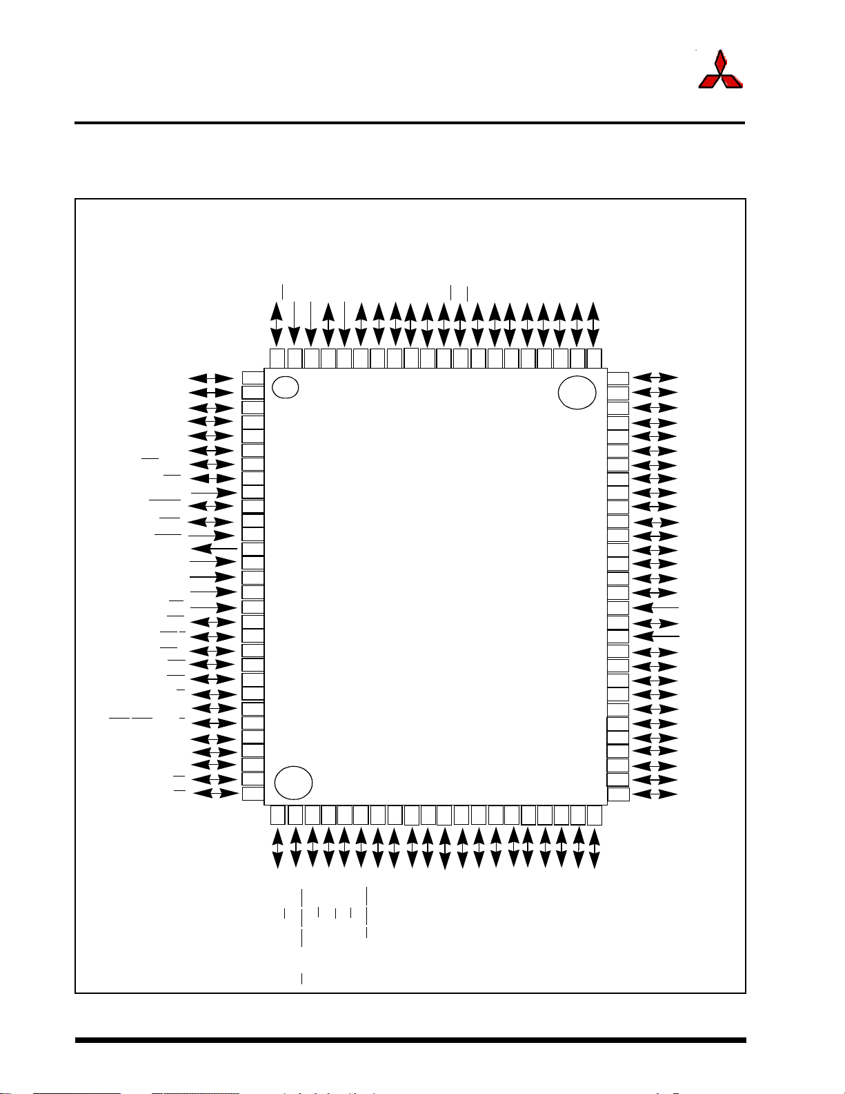
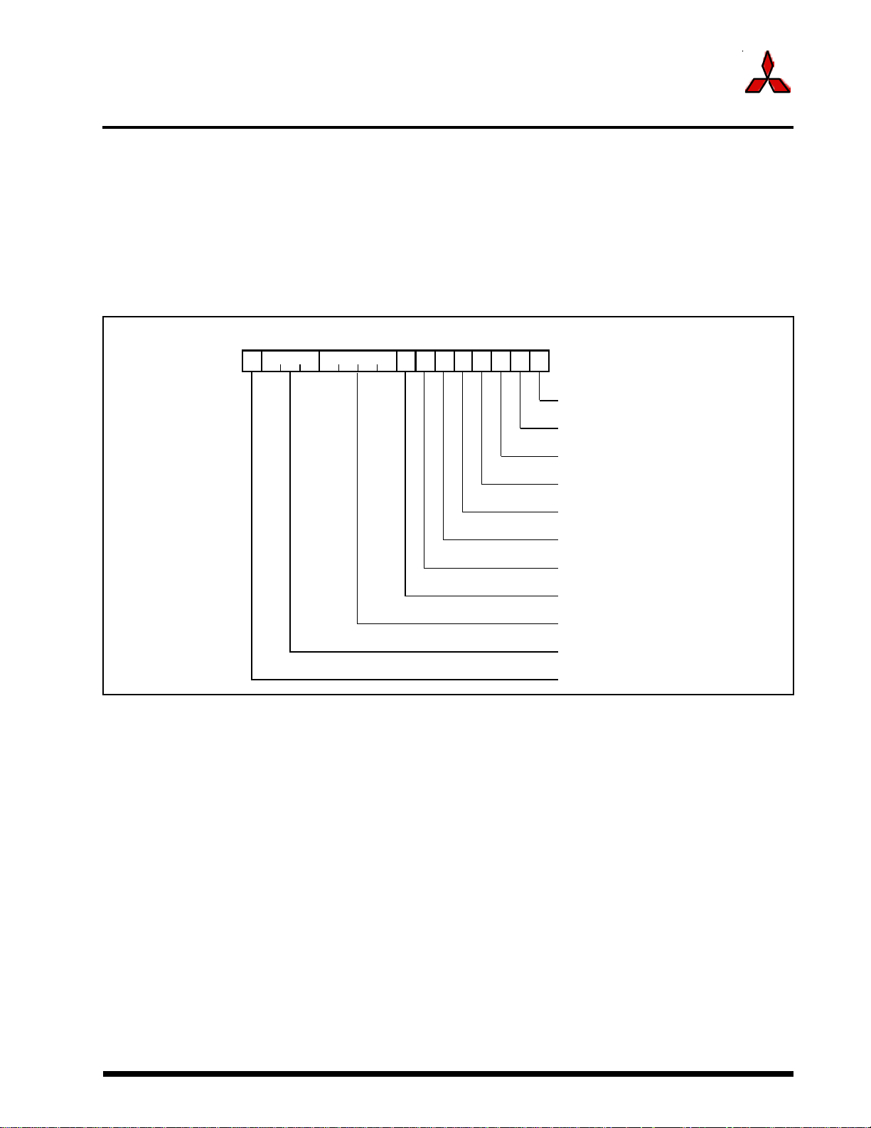
Pin Configuration
Figure 1.1 shows the pin configurations for M30222 group.
P97/ADtrg/LED7/Sin4/INT3
P100/AN0
P101/AN1
AVcc
Vref
AVss
MITSUBISHI MICROCOMPUTERS
M30222 Group
SINGLE-CHIP 16-BIT CMOS MICROCOMPUTER
P106/AN6/INT6
P107/AN7/INT7
P103/AN3
P102/AN2
P104/AN4
P105/AN5
VL1
VL2
VL3
COM2
COM0
COM1
C2
C1
P96/ANEX1/Sout4
P95/ANEX0/CLK4
P94/DA1/TB4in
P93/DA0/TB3in
P92/TB2in/Sout3
P91/TB1in/Sin3
P90/TB0in/INT2/CLK3
P86/INT1
CNVss
P85/Xcin
P84/Xcout
RESET
P83/NMI
P82/INT0
P81/TA4IN/INT5/U
P80/TA4OUT/INT5/U
P77/TA3IN/INT4
P76/TA3OUT/INT4
P75/TA2IN/W
P74/TA2OUT/W
P73/CTS2/RTS2/TA1IN/V
P72/CLK2/TA1OUT/V
P71/RxD2/SCL/TA0IN/TB5IN
P70/TxD2/SDA/TA0OUT
P67/TxD1/KI7
P66/RxD1/KI6
Xout
Vss
100
98
99
1
2
3
4
5
6
7
8
9
10
1211
13
14
Xin
V
cc
15
16
17
18
19
20
21
22
23
24
25
26
27
28
29
30
33
31
95
96
97
M30222FG
36
35
34
92
91
93
94
40
38
37
39
88
89
90
43
42
85
86
87
44
84
45
46
47
81
82
83
80
79
78
77
5758596061626364656667686970717273747576
53545556
52
51
49
48
50
COM3
SEG00
SEG01
SEG02
SEG03
SEG04
SEG05
SEG06
SEG07
SEG08
SEG09
SEG10
SEG11
SEG12
SEG13
SEG14
Vss
SEG15
VDC
Vcc
SEG16
SEG17
SEG18
SEG19
SEG20
SEG21
SEG22
SEG23
SEG24/P30
SEG25/P31
P65/CLK1/KI5
P64/CTS1/RTS1/CTS0/CLKS1/KI432
Fig. 1.1. Pin configuration (top view)
P61/CLK0/KI1
P63/TxD0/KI3
P62/RxD0/KI2
P60/CTS0/RTS0/KI0
SEG39/P47/RTP1
SEG37/P45
SEG38/P46/RTP0
SEG33/P41
SEG35/P4341SEG36/P44
SEG34/P42
SEG32/P40
SEG30/P36
SEG31/P37
SEG29/P35
SEG27/P33
SEG28/P34
SEG26/P32
1-4
Page 4
Under
development
Specifications in this manual are tentative and subject to change
Rev. G
Description
Block Diagram
Figure 1.2 is a block diagram of the M30222 group.
MITSUBISHI MICROCOMPUTERS
M30222 Group
SINGLE-CHIP 16-BIT CMOS MICROCOMPUTER
I/O ports
COM 0-3
Internal peripheral functions
Timer
Timer TA0 (16 bits)
Expandable up to 10 channels)
Timer TA1 (16 bits)
Timer TA2 (16 bits)
Timer TA3 (16 bits)
UART/clock synchronous SI/O
Timer TA4 (16 bits)
Timer TB0 (16 bits)
Timer TB1 (16 bits)
CRC
Timer TB2 (16 bits)
Timer TB3 (16 bits)
Timer TB4 (16 bits)
Timer TB5 (16 bits)
Watchdog timer
(15 bits)
DMAC
(2 channels)
D-A converter
(8 bits X 2 channels)
Note 1: ROM size depends on MCU type.
Note 2: RAM size depends on MCU type.
4
A-D converter
SEG 0-23
24
Port P3
SEG 24-31
(10 bits X 8 channels
(8 bits X 3 channels)
arithmetic circuit (CCITT
(Polynomial : X
16
+X
)
5
12
+1)
+X
M16C/60 series16-bit CPU core
Registers
R0LR0H
R0LR0H
R1H R1L
R1H R1L
R2
R2
R3
R3
A0
A0
A1
A1
FB
FB
SB FLG
Program counter
PC
Vector table
INTB
Stack pointer
ISP
USP
8
8
Port P4
SEG 32-39
System clock generator
IN-XOUT
X
X
CIN-XCOUT
Clock synchronous SI/O
(8 bits X 2 channels)
LCD Controller
VDC
Memory
ROM
(Note 1)
RAM
(Note 2)
Multiplier
Port P6
8
Port P7
8
Port P8
6
Port P8
3
Port P9
1
8
Port P10
8
Fig. 1.2. Block diagram of M30222 group
Memory Expansion
Figure 1.3 shows the Memory expansion for the M30222 group.
ROM size
(Bytes)
260K
128K
96K
64K
32K
M30222FC/FP/GP
20K SRAM
Flash Memory Version
Fig. 1.3. Memory Expansion
1-5
Page 5
Under
development
Specifications in this manual are tentative and subject to change
Rev. G
Description
Performance Outline
Table 1.1. Performance outline of the M30222 group
MITSUBISHI MICROCOMPUTERS
M30222 Group
SINGLE-CHIP 16-BIT CMOS MICROCOMPUTER
Parameters
Number of basic instructions 91
Shortest instruction execution time 62.5ns f(Xin) = 16MHz
ROM 260K bytes
Memory size
Input/Output
Multifunctional
timer
Serial I/O UART0, UART1, UART2
A-D converter 10 bits x (8 + 2) channels
D-A converter 8 bits x 2
CRC calculation circuit CRC-CCITT
RAM 20K bytes
P3-P4, P6-P10
except P83
P83 I 1 bit x 1
TA0, TA1, TA2, TA3, TA4 16 bits x 5
TB0, TB1, TB2, TB3, TB4, TB5 16 bits x 6, three-phase motor control
SIO3, SIO4 (Clock synchronous) x 2
I/O 8 bits x 6, 7 bits x 1
(UART or clock synchronous) x 3, or I
Functions
2
C x 1
Watchdog timer 15 bits x 1 (with prescaler)
Interrupts 25 external, 8 internal sources, 4 software, 7 levels
Clock generating circuit 2 built-in clock generation circuits
Supply voltage 2.7 to 5.5V f(Xin) = 16 MHz, without software wait
Power consumption TBD
I/O characteristics I/O withstand voltage 5.5V
P3, P4 0.1 mA (high output), 2.5 mA (low output)
Output current
P6-P10 5 mA at 5V (excluding pins P7
Device configuration CMOS high performance silicon gate
Package 100-pin plastic mold QFP
COM0 to COM3 4 lines
LCD
SEG0 to SEG39 40 lines (16 lines shared with I/O ports)
, P71, P83)
0
1-6
Page 6
Under
development
Specifications in this manual are tentative and subject to change
Rev. G
Description
Mitsubishi plans to release the following products in the M30222 group:
(1) Support for Flash memory version and mask ROM versions
(2) ROM capacity: 260 K bytes
(3) Package
100P6S-A : Plastic molded QFP (mask ROM version)
100P6Q-A: Plastic molded QFP
M16C Family Group
Figure 1.4 shows the M30222 family.
Type No. M 3 0 2 2 2 F G – X X X F P
MITSUBISHI MICROCOMPUTERS
M30222 Group
SINGLE-CHIP 16-BIT CMOS MICROCOMPUTER
Package type:
FP: Package 100P6S-A
GP: 100P6Q-A
ROM No.
Omitted for flash memory version
ROM capacity:
G: 260K bytes
Memory type:
F : Flash memory version
M30222 Group
Fig. 1.4. Type No., memory size, and package
Table 1.2 shows the product list for the M30222 family.
Table 1.2. Product list
Type No. ROM Capacity RAM Capacity Package Type Remarks
M30222FGFP 100P6S-A
M30222FGGP 100P6Q-A
260 Kbytes
20 Kbytes
M16C Family
Flash
1-7
Page 7
Under
development
Specifications in this manual are tentative and subject to change
Rev. G
Description
MITSUBISHI MICROCOMPUTERS
M30222 Group
SINGLE-CHIP 16-BIT CMOS MICROCOMPUTER
Pin Description
Table 1.3. Pin Description for M30222 group
Pin name Signal name I/O type Function
Vcc, Vss Power supply Input Supply 2.7 to 5.5V to the Vcc pin and 0V to Vss
VDC Voltage Down
CNVss CNVss
RESET
Xin, Xout Main Clock Input/Output These pins are provided for the main clock generating circuit. Connect a ceramic reso-
/P8
P8
4
5
Xcout/Xcin Subclock Input/Output
AVcc
AVss
Vref
P3
to P3
0
7
to P4
P4
0
7
to P6
P6
0
7
to P7
P7
0
7
Converter
Reset input Input An “L” on this input resets the microcomputer.
I/O Port Input/Output These pins are provided for the subclock generating circuit. Connect a ceramic reso-
Analog power
supply + reference
Analog power
supply + reference
Reference voltage
input
I/O Port P3 Input/Output This is an 8-bit CMOS I/O port. It has an input/output direction register that allows the
RTP0_0 to RTP3_1 Output
SEG24 to SEG31 Output Pins in this port also function as SEG output for LCD and output for Real-time port.
I/O Port P4 Input/Output This is an 8-bit I/O port equivalent to P3.
SEG32 to SEG39 Output Pins in Port 4 also function as SEG outputs for LCD.
RTP4_0 to RTP7_1 Output Pins in Port 4 also function as Real-time port.
I/O Port P6 Input/Output This is an 8-bit I/O port equivalent to P3.
to KI7 Input Pins in Port 6 also function as key-input interrupts.
KI0
UART0, UART1 Input/Output Pins in Port 6 also function as transmit, receive, clock, and CTS
I/O Port P7 Input/Output This is an 8-bit I/O port equivalent to P3.
UART2
Timer A/B Input/Output Some pins in Port 7 serve as input/output for Timer A and Timer B.
INT4
Input Connects capacitor from VDC to Vss; or if not using VDC, connect 3.3V to VDC pin.
This pin is used to enable flash programming. Connect the pull-down resistor from
CNVss to Vss. Connect CNVss to enable flash programming.
nator or crystal between the Xin and the Xout pins. To use an externally derived clock,
input it to the Xin.
nator or crystal between the Xcin pin and leave the Xcout pin open. These pins also
function as CMOS I/O ports.
Input
Input This pin is a power supply input for A-D converter. Connect this pin to Vss.
Input This pin is a reference voltage input for the A-D converter.
Input/Output Some pins in Port 7 serve as transmit, receive, clock, and CTS
Input Pins P76 and P77 function as inputs for INT4.
This pin is a power supply input for the A-D converter. Connect this pin to Vcc.
user to set each pin for input or output individually. When used for input, the port can
be set by software to have or not have a pull resistor in units of four bits.
UART1.
UART2 provides I
2
C serial communications.
/RTS pins for UART0,
/RTS for UART2.
to P82, P8
P8
0
P8
3
Three-phase Output Some pins in Port 7 function as three-phase outputs for V, V
I/O Port P8 Input/Output P80 to P82, P86 are I/O ports equivalent to P3.
Timer A Input/Output Some pins in Port 8 serve as input/output for Timer A and Timer B.
6
INT5
Three-phase Output Pins P80 and P81 function as inputs three-phase outputs for U and U.
NMI Input
Input Pins P80 and P81 function as inputs for INT5.
P8
is an input only port that also functions for NMI. The NMI interrupt is generated
3
when the input at this pin changes from “H” to “L”. The NMI
celled using software. The pull-up resistor cannot be set for this pin.
1-8
, W, and W.
function cannot be can-
Page 8
Under
development
Specifications in this manual are tentative and subject to change
Rev. G
Description
Pin name Signal name I/O type Function
I/O Port P9 Input/Output This is an 8-bit I/O equivalent to P3.
SIO 3/4 Input/Output Pins in Port 9 function as transmit, receive and clock for SIO3 and SIO4.
Timer B Input Some pins in Port 9 serve as TB3 and TB4 pins.
P9
to P9
0
7
D-A Output P9
, INT3 Input Pin P90 and P97 can be configured as INT2 and INT3.
INT2
MITSUBISHI MICROCOMPUTERS
M30222 Group
SINGLE-CHIP 16-BIT CMOS MICROCOMPUTER
and P94 can be configured to function as a digital to analog output.
3
ANEX0 Output
ANEX1 Input
I/O Port 10 Input/Output This is an 8-bit I/O port equivalent to P3.
to P10
P10
0
SEG23
SEG0 to
COM0 to COM3 COM ports Pins in this port function as COM output for LCD drive circuit.
VL1 to VL3 Power supply for
AN0 to AN7 Input Pins in Port 10 function as analog inputs.
7
INT6
, INT7 Input P106 and P107 function as inputs for INT6 and INT7.
SEG drive pins Pins in this port function as SEG output for LCD drive circuit.
LCD driver
These pins are used to connect to an optional external op amp.
Power supply input for LCD drive circuit.
1-9
Page 9
Under
development
Specifications in this manual are tentative and subject to change
Rev. G
Memory
Operation of Functional Blocks
The M30222 group accommodates certain units in a single chip. These units include ROM and RAM to
store instructions and data and the central processing unit (CPU) to execute arithmetic/logic operations.
Also included are peripheral units such as timers, serial I/O, D-A converter, DMAC, CRC calculation
circuit, A-D converter, LCD, and I/O ports. The following explains each unit.
Memory
Figure 1.5 is a memory map of the M30222 group. The linear address space of 1M bytes extends from
address 0000016 to FFFFF16. From FFFFF16 down is ROM. For example, in the M30222FG-XXXFP, there
is 256K bytes of internal ROM from C000016 to FFFFF16. The vector table for fixed interrupts such as the
reset and NMI are mapped to FFFDC16 to FFFFF16. The starting address of the interrupt routine is stored
here. The address of the vector table for timer interrupts, etc., can be set as desired using the internal
register (INTB). See the section on interrupts for details.
MITSUBISHI MICROCOMPUTERS
M30222 Group
SINGLE-CHIP 16-BIT CMOS MICROCOMPUTER
From 0040016 up is RAM. For example, in the M30222FG-XXXFP, 20K bytes of internal RAM is mapped
to the space from 0040016 to 053FF16. In addition to storing data, the RAM also stores the stack used
when calling subroutines and when interrupts are generated.
The SFR area is mapped to 0000016 to 003FF16. This area accommodates the control registers for periph-
eral devices such as I/O ports, A-D converter, serial I/O, and timers, etc. Tables 1.5 to 1.9 show the
location of peripheral unit control registers. Any part of the SFR area that is not occupied is reserved and
cannot be used for other purposes.
00000
16
SFR area
053FF
16
16
Type No. Address YYYYY
M30222MG/FG/GP
Address XXXXX
C0000
For details, see Tables
16
00400
XXXXX
16
D0000
16
YYYYY16
16
16
FFFFF
16
1.5-1.9
Internal RAM area
Internal reserved
area
Internal ROM area
FFE0016
FFFDC
FFFFF
Undefined instruction
16
BRK instruction
Address match
Watchdog timer
16
Special page
vector table
Overflow
Single step
DBC
NMI
Reset
Fig. 1.5. Memory Map
1-10
Page 10
Under
development
Specifications in this manual are tentative and subject to change
Rev. G
CPU
Central Processing Unit (CPU)
The CPU has a total of 13 registers shown in Figure 1.6. Seven of these registers (R0, R1, R2, R3, A0, A1,
and FB) come in two sets; therefore, these have two register banks.
MITSUBISHI MICROCOMPUTERS
M30222 Group
SINGLE-CHIP 16-BIT CMOS MICROCOMPUTER
b15
(Note)
R0
(Note)
R1
(Note)
R2
(Note)
R3
(Note)
A0
(Note)
A1
(Note)
FB
H
b15 b8 b7 b0
H
b15 b0
b15
b15
b15 b0
b15 b0
These registers consist of two register banks.
Note:
b8 b7 b0
L
L
b0
b0
Data
registers
Address
registers
Frame base
registers
IPL
PC
b19
INTB
HL
b15
USP
b15
ISP
b15 b0
SB
b15
FLG
b0 b19
Program counter
b0
Interrupt table
register
b0
User stack pointer
b0
Interrupt stack
pointer
Static base
register
b0
Flag register
CDZSBOIU
Fig. 1.6. Central Processing Unit Register
(1) Data registers (R0, R0H, R0L, R1, R1H, R1L, R2, and R3)
Data registers (R0, R1, R2, and R3) are configured with 16 bits, and are used primarily for transfer and
arithmetic/logic operations.
Registers R0 and R1 each can be used as separate 8-bit data registers, high-order bits as (R0H/R1H),
and low-order bits as (R0L/R1L). In some instructions, registers R2 and R0, as well as R3 and R1 can
use as 32-bit data registers (R2R0/R3R1).
(2) Address registers (A0 and A1)
Address registers (A0 and A1) are configured with 16 bits, and have functions equivalent to those of data
registers. These registers can also be used for address register indirect addressing and address register
relative addressing. In some instructions, registers A1 and A0 can be combined for use as a 32-bit
address register (A1A0).
(3) Frame base register (FB)
Frame base register (FB) is configured with 16 bits, and is used for FB relative addressing.
1-11
Page 11

Under
development
Specifications in this manual are tentative and subject to change
Rev. G
CPU
(4) Program counter (PC)
Program counter (PC) is configured with 20 bits, indicating the address of an instruction to be executed.
(5) Interrupt table register (INTB)
Interrupt table register (INTB) is configured with 20 bits, indicating the start address of an interrupt vector
table.
(6) Stack pointer (USP/ISP)
Stack pointer comes in two types: user stack pointer (USP) and interrupt stack pointer (ISP), each
configured with 16 bits. Your desired type of stack pointer (USP or ISP) can be selected by a stack
pointer select flag (U flag). This flag is located at the position of bit 7 in the flag register (FLG).
(7) Static base register (SB)
Static base register (SB) is configured with 16 bits, and is used for SB relative addressing.
MITSUBISHI MICROCOMPUTERS
M30222 Group
SINGLE-CHIP 16-BIT CMOS MICROCOMPUTER
(8) Flag register (FLG)
Flag register (FLG) is configured with 11 bits, each bit is used as a flag. Figure 1.7 shows the flag
register (FLG). The following explains the function of each flag:
• Bit 0: Carry flag (C flag)
This flag retains a carry, borrow, or shift-out bit that has occurred in the arithmetic/logic unit.
• Bit 1: Debug flag (D flag)
This flag enables a single-step interrupt.
When this flag is “1”, a single-step interrupt is generated after instruction execution. This flag is cleared to
“0” when the interrupt is acknowledged.
• Bit 2: Zero flag (Z flag)
This flag is set to “1” when an arithmetic operation resulted in 0; otherwise, cleared to “0”.
• Bit 3: Sign flag (S flag)
This flag is set to “1” when an arithmetic operation resulted in a negative value; otherwise, cleared to “0”.
• Bit 4: Register bank select flag (B flag)
This flag chooses a register bank. Register bank 0 is selected when this flag is “0” ; register bank 1 is
selected when this flag is “1”.
• Bit 5: Overflow flag (O flag)
This flag is set to “1” when an arithmetic operation resulted in overflow; otherwise, cleared to “0”.
• Bit 6: Interrupt enable flag (I flag)
This flag enables a maskable interrupt.
An interrupt is disabled when this flag is “0”, and is enabled when this flag is “1”. This flag is cleared to “0”
when the interrupt is acknowledged.
• Bit 7: Stack pointer select flag (U flag)
Interrupt stack pointer (ISP) is selected when this flag is “0” ; user stack pointer (USP) is selected when this
flag is “1”.
This flag is cleared to “0” when a hardware interrupt is acknowledged or an INT instruction of software
interrupt Nos. 0 to 31 is executed.
1-12
Page 12
Under
development
Specifications in this manual are tentative and subject to change
Rev. G
CPU
• Bits 8 to 11: Reserved area
• Bits 12 to 14: Processor interrupt priority level (IPL)
Processor interrupt priority level (IPL) is configured with three bits, for specification of up to eight processor
interrupt priority levels from level 0 to level 7.
If a requested interrupt has priority greater than the processor interrupt priority level (IPL), the interrupt is
enabled.
• Bit 15: Reserved area.
IPL
MITSUBISHI MICROCOMPUTERS
M30222 Group
SINGLE-CHIP 16-BIT CMOS MICROCOMPUTER
b0b15
CDZSBOIU
Flag register (FLG)
Carry flag
Debug flag
Zero flag
Fig. 1.7. Flag Register
Sign flag
Register bank select flag
Overflow flag
Interrupt enable flag
Stack pointer select flag
Reserved area
Processor interrupt priorit
Reserved area
1-13
Page 13
Under
development
Specifications in this manual are tentative and subject to change
Rev. G
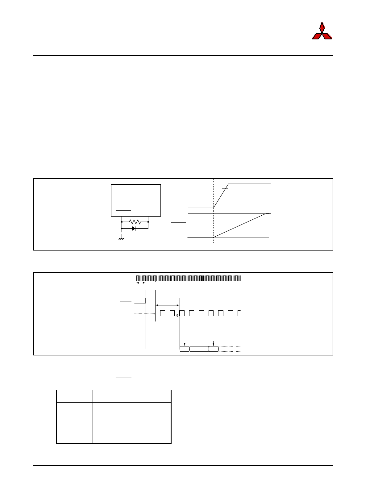
Reset
Reset
There are two kinds of resets; hardware and software. In both cases, operation is the same after the
reset. (See “Software Reset” for details.) This section explains on hardware resets.
When the supply voltage is in the range where operation is guaranteed, a reset is effected by holding the
reset pin level “L” (0.2VCC max.) for at least 20 cycles. When the reset pin level is then returned to the
“H” level while main clock is stable, the reset status is cancelled and program execution resumes from
the address in the reset vector table.
Figure 1.8 shows an example reset circuit. Figure 1.9 shows a reset sequence. Table 1.4 shows the pin
status when reset pin level is "L".
MITSUBISHI MICROCOMPUTERS
M30222 Group
SINGLE-CHIP 16-BIT CMOS MICROCOMPUTER
RESET
Example when Vcc = 5V
Fig. 1.8. Example of Reset Circuit
in
X
RESET
BCLK
Address
Fig. 1.9. Reset sequence
V
CC
More than 20
cycles are
BCLK
24cycles
5V
V
CC
0V
5V
RESET
0V
needed
FFFFC
16
FFFFE
Content of reset
vector
16
4.0V
0.8V
Table 1.4. Pin status when Reset pin level is "L"
level
Status
is
output
Pin name
P3, P4
P6 to P10
SEG0 to SEG23
COM0 to COM3
Input port (with a pull-up resistor)
Input port (floating)
"H" level is output
"H"
1-14
Page 14
Under
development
MITSUBISHI MICROCOMPUTERS
Specifications in this manual are tentative and subject to change
Rev. G
Special function registers
SINGLE-CHIP 16-BIT CMOS MICROCOMPUTER
Special function registers
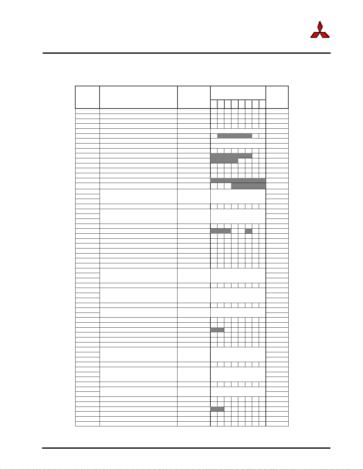
Table 1.5. Location and value after reset of peripheral unit control registers (1)
M30222 Group
Address Register Name Acronym
0000
16
0001
16
0002
16
0003
16
000416Processor mode register 0 PM0
000516Processor mode register 1 PM1
000616System clock control register 0 CM0
000716System clock control register 1 CM1
0008
16
000916Address match interrupt enable register AIER
000A16Protect register PRCR
000B
16
000C
16
000D
16
000E16Watchdog timer start register WDTS 1.57
000F16Watchdog timer control register WDC
0010
16
0011
0012
0013
0014
0015
0016
0017
001816VDC control register VDCC
0019
001A
001B
001C
001D
001E
001F
0020
0021
0022
0023
0024
0025
0026
0027
0028
0029
002A
002B
002C16DMA0 control register DM0CON
002D
002E
002F
0030
0031
0032
0033
0034
0035
0036
0037
0038
0039
003A
003B
003C16DMA1 control register DM1CON
003D
003E
003F
Address match interrupt register 0 RMAD0
16
16
16
16
Address match interrupt register 1 RMAD1
16
16
16
16
16
16
16
16
16
16
16
DMA0 source pointer SAR0
16
16
16
16
DMA0 destination pointer DAR0
16
16
16
DMA0 transfer counter TRC0
16
16
16
16
16
16
16
16
DMA1 source pointer SAR1
16
16
16
16
DMA1 destination pointer DAR1
16
16
16
DMA1 transfer counter TCR1
16
16
16
16
16
16
16
Value after ResetSFR
b7 b6 b5 b4 b3 b2 b1 b0
00
000
000
16
48
16
20
16
0000
00
16
00
16
00 00
?
?
?
000000
?
?
?
000000
Number
00
? = Undefined
Page
1.19
1.19
1.23
1.23
1.53
1.34
1.57
1.53
1.53
1.53
1.53
1.53
1.53
1.29
1.62
1.62
1.62
1.62
1.62
1.62
1.62
1.62
1.61
1.62
1.62
1.62
1.62
1.62
1.62
1.62
1.62
1.61
1-15
Page 15
Under
development
MITSUBISHI MICROCOMPUTERS
Specifications in this manual are tentative and subject to change
Rev. G
Special function registers
SINGLE-CHIP 16-BIT CMOS MICROCOMPUTER
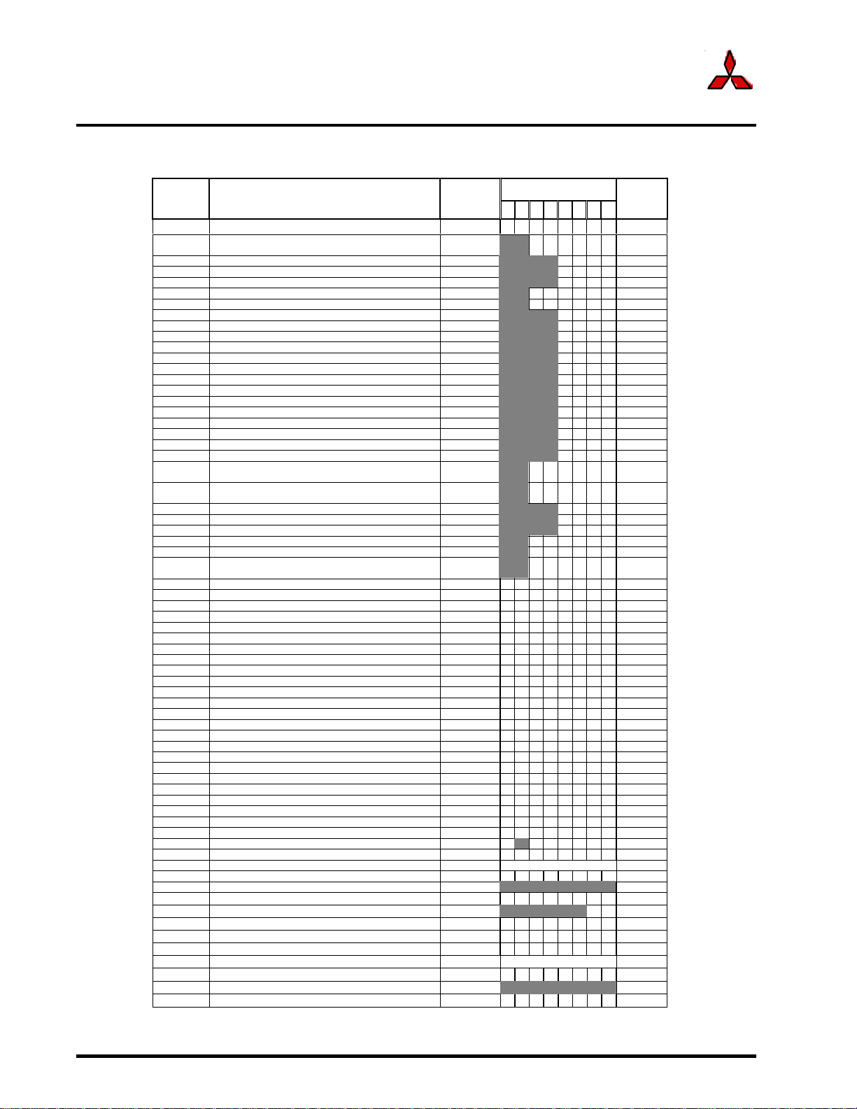
Table 1.6. Location and value after reset of peripheral unit control registers (2)
M30222 Group
Address
0044
0045
0046
0047
0048
0049
004A
004B
004C
004D
004E
004F
0050
0051
0052
0053
0054
0055
0056
0057
0058
0059
005A
005B
005C
005D
005E
005F
Register Name Acronym
INT3 interrupt control register
16
SI/O4 interrupt control register
Timer B5 interrupt control register TB5IC
16
Timer B4 interrupt control register TB 4IC
16
Timer B3 interrupt control register TB3IC
16
INT7 interrupt control register INT7IC
16
INT6 interrupt control register INT6IC
16
Bus collision detection interrupt control register BCNIC
16
DMA0 interrupt control register DM0IC
16
DMA1 interrupt control register DM1IC
16
Key input interrupt control register KUPIC
16
A-D conversion interrupt control register ADIC
16
UART2 transmit interrupt control register S2TIC
16
UART2 receive interrupt control register S2RIC
16
UART0 transmit interrupt control register S0TIC
16
UART0 receive interrupt control register S0RIC
16
UART1 transmit interrupt control register S1TIC
16
UART1 receive interrupt control register S1RIC
16
Timer A0 interrupt control register TA0IC
16
Timer A1 interrupt control register TA1IC
16
Timer A2 interrupt control register TA2IC
16
Timer A3 interrupt control register
16
INT4 interrupt control register
Timer A4 interrupt control register
16
INT5 interrupt control register
Timer B0 interrupt control register TB0IC
16
Timer B1 interrupt control register TB1IC
16
Timer B2 interrupt control register TB2IC
16
INT0 interrupt control register INT0IC
16
INT1 interrupt control register INT1IC
16
INT2 interrupt control register
16
SI/O3 interrupt control register
INT3IC
S4IC
TA3IC
INT4IC
TA4IC
INT5IC
INT2IC
S3IC
Value after ResetSFR
b7 b6 b5 b4 b3 b2 b1 b0
000000
0000
0000
0000
000000
000000
0000
0000
0000
0000
0000
0000
0000
0000
0000
0000
0000
0000
0000
0000
000000
000000
0000
0000
0000
000000
000000
000000
Page
Number
1.39
1.39
1.39
1.39
1.39
1.39
1.39
1.39
1.39
1.39
1.39
1.39
1.39
1.39
1.39
1.39
1.39
1.39
1.39
1.39
1.39
1.39
1.39
1.39
1.39
1.39
1.39
1.39
0100
0101
0102
0103
0104
0105
0106
0107
0108
0109
010A
010B
010C
010D
010E
010F
0110
0111
0112
0113
0120
0121
0122
0123
0124
0125
0126
0127
0128
0129
0130
0131
0132
0133
LCD RAM0 LRAM0
16
LCD RAM1 LRAM1
16
LCD RAM2 LRAM2
16
LCD RAM3 LRAM3
16
LCD RAM4 LRAM4
16
LCD RAM5 LRAM5
16
LCD RAM6 LRAM6
16
LCD RAM7 LRAM7
16
LCD RAM8 LRAM8
16
LCD RAM9 LRAM9
16
LCD RAM10 LRAM10
16
LCD RAM11 LRAM11
16
LCD RAM12 LRAM12
16
LCD RAM13 LRAM13
16
LCD RAM14 LRAM14
16
LCD RAM15 LRAM15
16
LCD RAM16 LRAM16
16
LCD RAM17 LRAM17
16
LCD RAM18 LRAM18
16
LCD RAM19 LRAM19
16
LCD mode register LCDM
16
16
Segment output enable register SEG
16
16
LCD frame frequency counter LCDTIM 1.143
16
16
Key input mode register KUPM
16
16
16
16
LCD expansion register LEXP
16
16
LCD clock divide counter LCDC 1.144
16
16
????????
????????
????????
????????
????????
????????
????????
????????
????????
????????
????????
????????
????????
????????
????????
????????
????????
????????
????????
????????
0 000000
00
16
00
16
? = Undefined
00
1.146
1.146
1.146
1.146
1.146
1.146
1.146
1.146
1.146
1.146
1.146
1.146
1.146
1.146
1.146
1.146
1.146
1.146
1.146
1.146
1.143
1.143
1.52
1.144
1-16
Page 16
Under
development
MITSUBISHI MICROCOMPUTERS
Specifications in this manual are tentative and subject to change
Rev. G
Special function registers
SINGLE-CHIP 16-BIT CMOS MICROCOMPUTER
Table 1.7. Location and value after reset of peripheral unit control registers (3)
M30222 Group
Address
Register Name Acronym
034016Timer B3, 4, 5 count start flag TBSR
0341
16
0342
0343
0344
0345
0346
0347
Timer A1-1 register TA11 1.94
16
16
Timer A2-1 register TA21 1.94
16
16
Timer A4-1 register TA41 1.94
16
16
034816Three-phase PWM control register 0 INVC0
034916Three-phase PWM control register 1 INVC1
034A16Three-phase output buffer register 0 IDB0
034B16Three-phase output buffer register 1 IDB1
Value after ResetSFR
b7 b6 b5 b4 b3 b2 b1 b0
000
00
16
00
16
3F
16
3F
16
Page
Number
1.85
1.92
1.92
1.93
1.93
034C16Dead time timer DTT 1.93
034D16Timer B2 interrupt occurrence frequency set counter ICTB2 1.93
034E
16
034F
16
0350
16
0351
0352
0353
0354
0355
035B16Timer B3 mode register TB3MR
Timer B3 register TB3 1.85
16
16
Timer B4 register TB4 1.85
16
16
Timer B5 register TB5 1.85
16
00 0000
1.87
1.88,
1.90
035C16Timer B4 mode register TB4MR
00 0000
1.87
1.88,
1.90
035D16Timer B5 mode register TB5MR
035E16Interrupt cause select register 0 IFSR0
035F16Interrupt cause select register 1 IFSR1
00 0000
00
16
00
16
1.87
1.88,
1.90
1.49
1.49
036016SI/O3 transmit/receive register S3TRR 1.138
0361
16
036216SI/O3 control register S3C
40
16
1.138
036316SI/O3 bit rate generator S3BRG 1.138
036416SI/O4 transmit/receive register S4TRR 1.138
0365
16
036616SI/O4 control register S4C
40
16
1.138
036716SI/O4 bit rate generator S4BRG 1.138
036C16Clock divided control register CDCC
036D
16
0
1.24
036E16Clock divided counter CDC 1.24
037516UART2 special mode register 3 U2SMR3
037616UART2 special mode register 2 U2SMR2
037716UART2 special mode register U2SMR
037816UART2 transmit/receive mode register U2MR
00
16
00
16
00
16
00
16
1.112
1.130
1.112,
1.134
1.111,
1.130
1.108,
1.114,
1.120
037916UART2 bit rate generator U2BRG 1.107
037A
16
037B
037C16UART2 transmit/receive control register 0 U2C0
037D16UART2 transmit/receive control register 1 U2C1
037E
037F
UART2 transmit buffer register U2TB 1.107
16
16
UART2 receive buffer register U2RB 1.102
16
08
16
02
16
1.110
? = Undefined
1-17
Page 17
Under
development
Specifications in this manual are tentative and subject to change
Rev. G
Special function registers
MITSUBISHI MICROCOMPUTERS
M30222 Group
SINGLE-CHIP 16-BIT CMOS MICROCOMPUTER
SFR
Address
038016Count start flag TABSR
038116Clock prescaler reset flag CPSRF
Register Name Acronym
038216One-shot start flag ONSF
038316Trigger select register TRGSR
038416Up-down flag UDF
0385
16
0386
0387
0388
0389
038A
038B
038C
038D
038E
038F
0390
0391
0392
0393
0394
0395
039616Timer A0 mode register TA0MR
Timer A0 TA0
16
16
Timer A1 TA1
16
16
Timer A2 TA2
16
16
Timer A3 TA3
16
16
Timer A4 TA4
16
16
Timer B0 TB0
16
16
Timer B1 TB1
16
16
Timer B2 TB2
16
16
039716Timer A1 mode register TA1MR
039816Timer A2 mode register TA2MR
039916Timer A3 mode register TA3MR
039A16Timer A4 mode register TA4MR
039B16Timer B0 mode register TB0MR
039C16Timer B1 mode register TB1MR
039D16Timer B2 mode register TB2MR
039E
16
039F
16
03A016UART0 transmit/receive mode register U0MR
03A116UART0 bit rate generator U0BRG 1.107
03A2
03A3
03A416UART0 transmit/receive control register 0 U0C0
03A516UART0 transmit/receive control register 1 U0C1
03A6
03A7
03A816UART1 transmit/receive mode register U1MR
03A916UART1 bit rate generator U1BRG 1.107
03AA
03AB
03AC16UART1 transmit/receive control register 0 U1C0
03AD16UART1 transmit/receive control register 1 U1C1
03AE
03AF
03B016UART transmit/receive control register 2 UCON
03B1
03B2
03B3
03B416Flash memory control register (Note) FMCR
03B5
03B6
03B7
03B816DMA0 request cause select register DM0SL
03B9
03BA16DMA1 DM1SL
03BB
03BC
03BD
03BE16CRC input register CRCIN 1.164
UART0 transmit buffer register U0TB 1.107
16
16
UART0 receive buffer register U0RB 1.107
16
16
16
UART1 transmit buffer register U1TB 1.107
16
16
UART1 receive buffer register U1RB 1.107
16
16
16
16
16
16
16
16
16
16
CRC data register
16
CRCD
Value after Reset
b7 b6 b5 b4 b3 b2 b1 b0
00
0
00 00000
00 0000
00 0000
00 0000
0000000
16
00
16
00
16
00
16
00
16
00
16
00
16
00
16
00
16
08
16
02
16
00
16
08
16
02
16
0001
00
16
00
16
1.71, 1.85, 1.94
1.72, 1.85
1.72
1.72, 1.94
1.71
1.71
1.71, 1.90
1.71, 1.90
1.71
1.71, 1.90
1.83
1.83
1.83, 1.90
1.70, 1.73, 1.74,
1.77, 1.78
1.70, 1.73, 1.74,
1.77, 1.78, 1.95
1.70, 1.73, 1.74,
1.77, 1.78, 1.95
1.70, 1.72, 1.73,
1.77, 1.78
1.70, 1.73, 1.74,
1.77, 1.78, 1.95
1.84, 1.87, 1.90
1.84, 1.87, 1.90
1.84, 1.87, 1.90,
1.95
1.108, 1.114,
1.120
1.109
1.110
1.108, 1.114,
1.120
1.109
1.110
1.111
1.176
1.60
1.61
1.164
Note: This register only exists in flash memory version
? = Undefined
Page Number
1-18
Page 18
Under
development
MITSUBISHI MICROCOMPUTERS
Specifications in this manual are tentative and subject to change
Rev. G
Special function registers
Table 1.8. Location and value after reset of peripheral unit control registers (4)
Table 1.9. Location and value after reset of peripheral unit control registers (5)
SINGLE-CHIP 16-BIT CMOS MICROCOMPUTER
M30222 Group
Address
03C0
16
03C1
03C2
03C3
03C4
03C5
03C6
03C7
03C8
03C9
03CA
03CB
03CC
03CD
03CE
03CF
03D0
03D1
03D2
03D3
03D416A-D control register 2 ADCON2
03D5
A-D register 0 AD0
16
16
A-D register 1 AD1
16
16
A-D register 2 AD2
16
16
A-D register 3 AD3
16
16
A-D register 4 AD4
16
16
A-D register 5 AD5
16
16
A-D register 6 AD6
16
16
A-D register 7 AD7
16
16
16
16
16
16
Register Name Acronym
03D616A-D control register 0 ADCON0
03D716A-D control register 1 ADCON1
Value after ResetSFR
b7 b6 b5 b4 b3 b2 b1 b0
0000
00000
00
16
Page Number
0
1.153, 1.155,
1.156, 1.157,
1.158, 1.159
1.153, 1.155,
1.156, 1.157,
1.158, 1.159
1.154
1.154
1.154
1.154
1.154
1.154
1.154
1.154
1.154
03D816D-A register 0 DA0 1.163
03D9
16
03DA16D-A register 1 DA1 1.163
03DB
16
03DC16D-A control register DACON
03DD
16
03DE
16
03DF
16
03E0
16
03E1
16
03E2
16
03E3
16
03E4
16
03E516Port P3 P3 1.170
03E6
16
03E716Port P3 direction register PD3
00
16
00
16
1.163
1.170
03E816Port P4 P4 1.170
03E9
16
03EA16Port P4 direction register PD4
03EB
16
03EC16Port P6 P6 1.170
03ED16Port P7 P7 1.170
03EE16Port P6 direction register PD6
03EF16Port P7 direction register PD7
03F016Port P8 P8
03F116Port P9 P9 1.170
03F216Port P8 direction register PD8
03F316Port P9 direction register PD9
00
16
00
16
00
000000
0 0000
16
00
16
1.170
1.170
1.170
0
1.170
0
1.170
1.170
03F416Port P10 P10 1.170
03F5
16
03F616Port P10 direction register PD10
03F7
16
03F8
16
03F9
16
03FA
16
03FB
16
03FC16Pull-up control register 0 PUR0
03FD16Pull-up control register 1 PUR1
03FE16Pull-up control register 2 PUR2
03FF16Real-time port control register RTP
00
16
00
16
00
16
00
16
000
1.170
1.171
1.171
1.171
0
1.83
? = Undefined
1-19
Page 19
Under
development
Specifications in this manual are tentative and subject to change
Rev. G
Software Reset
Software Reset
Writing “1” to bit 3 of the processor mode register 0 (address 000416) applies a (software) reset to the
microcomputer. A software reset has the same effect as a hardware reset. The contents of internal RAM
are preserved.
Figure 1.10 shows processor mode register 0 and 1.
Processor mode register 0 (Note)
b7 b6 b5 b4 b3 b2 b1 b0
0
0
0
Symbol Address When reset
PM0 0004
MITSUBISHI MICROCOMPUTERS
M30222 Group
SINGLE-CHIP 16-BIT CMOS MICROCOMPUTER
16
00
16
Nothing is assigned.
Write "0" when writing to this these bits. If read, the value is indeterminate.
PM03
Nothing is assigned.
Write "0" when writing to this these bits. If read, the value is indeterminate.
Reserved bit Must always be set to "0"
Note : Set bit 1 of the protect register (address 000A
values to this register.
Processor mode register 1 (Note )
b7 b6 b5 b4 b3 b2 b1 b0
0
0
0
Note : Set bit 1 of the protect register (address 000A16) to “1” when writing new values
Symbol
PM1
Reserved bit
Nothing is assigned.
Write "0" when writing to this these bits. If read, the value is indeterminate.
PM17
to this register.
Bit name FunctionBit symbol
Software reset
Bit name FunctionBit symbol
Wait bit
bit
Address
0005
16
The device is reset when this bit is set
to “1”. The value of this bit is “0” when
read.
16
) to “1” when writing new
Must always be set to “0”
0 : No wait state
1 : Wait state inserted
When reset
0XXXXX00
2
WR
WR
O O
Fig. 1.10. Processor mode register 0 and 1
1-20
Page 20
Under
development
Specifications in this manual are tentative and subject to change
Rev. G
Clock Generating Circuit
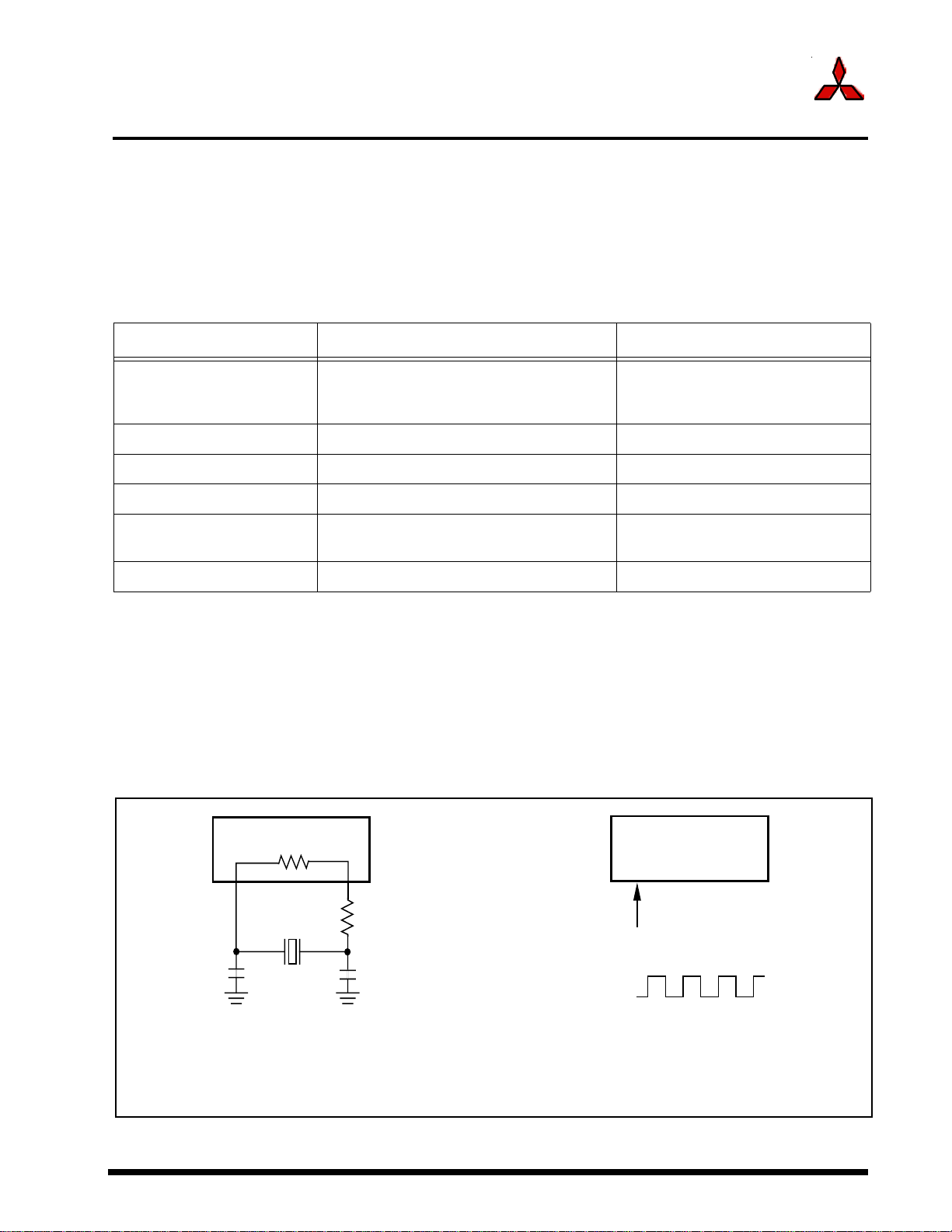
Clock generating Circuit
The clock generating circuit contains two oscillator circuits that supply the operating clock sources to
the CPU and internal peripheral units. Table 1.10 shows some examples of the main clock and
subclock generating circuits.
Table 1.10. Main clock and sub-clock generating circuits
Main clock generating circuit Sub-clock generating circuit
MITSUBISHI MICROCOMPUTERS
M30222 Group
SINGLE-CHIP 16-BIT CMOS MICROCOMPUTER
Use of clock Operating clock source for CPU
Operating clock source for Internal
peripheral
Usable oscillator Ceramic or crystal oscillator Crystal oscillator
Pins to connect oscillator Xin, Xout Xcin, Xcout
Oscillation stop/restart function Available Available
Oscillator status immediately
after Reset
Other Externally derived clock can be input (Note)
Note: Max. voltage is the same as VDC
Oscillating Stopped
Operating clock source
Count clock source for Timers A/B
Operating clock source for LCD
Figure 1.11 shows some examples of the main clock circuit, one using an oscillator connected to the
circuit, and the other one using an externally derived clock for input. Figure 1.12 shows some ex-
amples of sub-clock circuits, one using an oscillator connected to the circuit, and the other one using
an externally derived clock for input. Circuit constants in Figures 1.11 and 1.12 vary with each oscil-
lator used. Use the values recommended by the manufacturer of your oscillator.
Microcomputer
(Built-in feedback resistor)
Xin
Cin
Note: Insert a damping resistor if required. The resistance will vary depending on the oscillator and the oscillation drive
capacity setting. Use the value recommended by the maker of the oscillator.
When the oscillation drive capacity is set to low, check that oscillation is stable. Also, if the oscillator manufacturer's
data sheet specifies that a feedback resistor be added external to the chip, insert a feedback resistor between X
and X
Fig. 1.11. Examples of main clock
Xout
(Note)
Rd
out
following the instruction.
Cout
Microcomputer
Xin Xout
Open
Externally derived clock
Vcc
Vss
in
1-21
Page 21
Under
development
Specifications in this manual are tentative and subject to change
Rev. G
Clock Generating Circuit
MITSUBISHI MICROCOMPUTERS
M30222 Group
SINGLE-CHIP 16-BIT CMOS MICROCOMPUTER
Microcomputer
(Built-in feedback resistor)
X
cin
X
cout
(Note 1)
R
C
cin
Note 1: Insert a damping resistor if required. The resistance will vary depending on the oscillator and the oscillation drive
capacity setting. Use the value recommended by the maker of the oscillator.
When the oscillation drive capacity is set to low, check that oscillation is stable. Also, if the oscillator manufacturer's
data sheet specifies that a feedback resistor be added external to the chip, insert a feedback resistor between X
and X
cout
following the instruction.
Note 2: Reference XCin to VDC supply.
C
cout
Fig. 1.12. Examples of sub-clock
Figure 1.13 shows a block diagram of the clock generating circuit.
X
CIN
X
COUT
CM04
Sub clock
RESET
Software reset
NMI
Interrupt request
level judgment
output
CM10 "1"
Write signal
WAIT instruction
Q
S
R
QS
R
CM05
X
IN
Main clock
X
OUT
CM02
VDC
1/32
Microcomputer
X
cin
Externally derived clock
(Note 2)
Vss
CM14=1
f
C1
C32
f
f
C
a
CM14=0
f
1
f
AD
c
b
Divider
f
C132
f
f
32
d
f
C
X
cout
Open
8
CM07=0
CM07=1
cin
BCLK
CM0i : Bit i at address 0006
CM1i : Bit i at address 0007
WDCi : Bit i at address 000F
Fig. 1.13. Clock generating circuit
b
a
16
16
16
1/2 1/2 1/2 1/2
CM06=1
CM06=0
CM17,CM16=01
CM06=0
CM17,CM16=00
CM06=0
CM17,CM16=10
CM06=0
CM17,CM16=11
Details of divider
c
1/2
d
1-22
Page 22

Under
development
Specifications in this manual are tentative and subject to change
Rev. G
Clock Generating Circuit
The following paragraphs describes the clocks generated by the clock generating circuit.
(1) Main clock
The main clock is generated by the main clock oscillation circuit. After a reset, the clock is divided by 8 to
the BCLK. The clock can be stopped using the main clock stop bit (bit 5 at address 0006
clock, after switching the operating clock source of CPU to the sub-clock, reduces the power dissipation.
After the oscillation of the main clock oscillation circuit has stabilized, the drive capacity of the main clock
oscillation circuit can be reduced using the X
Reducing the drive capacity of the main clock oscillation circuit reduces the power dissipation. This bit
changes to “1” when shifting from high-speed/medium-speed mode to stop mode and at a reset. When
shifting from low-speed/low power dissipation mode to stop mode, the value before stop mode is retained.
(2) Sub-clock
The sub-clock is generated by the sub-clock oscillation circuit. No sub-clock is generated after a reset. After
oscillation is started using the port Xc select bit (bit 4 at address 0006
the BCLK by using the system clock select bit (bit 7 at address 0006
oscillation has fully stabilized before switching.
MITSUBISHI MICROCOMPUTERS
M30222 Group
SINGLE-CHIP 16-BIT CMOS MICROCOMPUTER
16). Stopping the
IN-XOUT drive capacity select bit (bit 5 at address 000716).
16), the sub-clock can be selected as
16). However, be sure that the sub-clock
After the oscillation of the sub-clock oscillation circuit has stabilized, the drive capacity of the sub-clock
oscillation circuit can be reduced using the XCIN-XCOUT drive capacity select bit (bit 3 at address 000616).
Reducing the drive capacity of the sub-clock oscillation circuit reduces the power dissipation. This bit changes
to “1” when shifting to stop mode and at a reset.
(3) BCLK
The BCLK is the clock that drives the CPU, and is fc or the clock is derived by dividing the main clock by 1, 2,
4, 8, or 16. The BCLK is derived by dividing the main clock by 8 after a reset.
The main clock division select bit 0(bit 6 at address 0006
medium-speed to stop mode and at reset. When shifting from low-speed/low power dissipation mode to stop
mode, the value before stop mode is retained.
16) changes to “1” when shifting from high-speed/
(4) Peripheral function clock (f1, f8, f32, fAD)
The clock for the peripheral devices is derived from the main clock or by dividing it by 1, 8, or 32. The periph-
eral function clock is stopped by stopping the main clock or by setting the WAIT peripheral function clock stop
bit (bit 2 at 000616) to “1” and then executing a WAIT instruction.
(5) fC132
This clock is derived by dividing the sub-clock by 1 or 32. The clock is selected by fC132 clock select bit (bit4
at address 0007
16). It is used for the Timer A and Timer B counts, intermittent pull up operation of key input.
(6) fC
This clock has the same frequency as the sub-clock. It is used for the BCLK and for the Watchdog timer.
Figure 1.14 shows the system clock control registers 0 and 1.
1-23
Page 23
Under
development
Specifications in this manual are tentative and subject to change
Rev. G
Clock Generating Circuit
System clock control register 0 (Note 1)
b7 b6 b5 b4 b3 b2 b1 b0
Symbol Address When reset
CM0 0006
16
MITSUBISHI MICROCOMPUTERS
M30222 Group
SINGLE-CHIP 16-BIT CMOS MICROCOMPUTER
48
16
CM00
CM01
CM02
CM03
CM04
CM05
CM06
CM07
Bit name FunctionBit symbol
Clock output function
select bits
WAIT peripheral function
clock stop bit
Xcin-Xout drive capacity
select bit (Note 2)
Port Xc Select Bit
Main clock (Xin-X
stop bit (Note 3, 4)
Main clock division select
bit 0 (Note 6)
System clock select bit
(Note 5)
out
)
b1 b0
0 0 : I/O port P7
0 1 : fC1 output
1 0 : f
1
1 1 : Clock divide counter output
0 : Do not stop peripheral function clock in wait mode
1 : Stop peripheral function clock in wait mode (Note 7)
0 : LOW
1 : HIGH
0 : I/O port
1 : Xcin - Xcout generation
0 : Main clock on
1 : Main clock off
0 : CM16 and CM17 valid
1 : Division by 8 mode
Xin, Xout
0 :
Xcin, Xcout1 :
5
output
WR
Note 1: Set bit 0 of the protect register (address 000A16) to "1" before writing to this register.
Note 2: Changes to "1" when shifting to stop mode and at a reset.
Note 3: When inputting external clock, only clock oscillation buffer is stopped and clock input is acceptable.
Note 4: If this bit is set to "1", X
pulled up to X
Note 5: Set subclock (X
from "0" to "1". Do not write to both bits at the same time. Likewise, set the main clock stop bit (CM05) to "0" and
out
out
("H") via the feedback resistor.
cin
turns "H". The built-in feedback resistor remains being connected, so XIN turns
- X
) enable bit (CM04) to "1" and allow the subclock to stabilize before setting CM07 from
cout
allow the subclock to stabilize before settng CM07 bit from "1" to "0".
Note 6: This bit changes to "1" when shifting from high-speed/medium-speed mode to stop mode and at a reset. When
shifting from low-speed/low power dissipation mode to stop mode, the value before stop mode is retained.
C
, f
C132
, fC1, f
C32
Note 7: f
is not included.
System clock control register 1 (Note 1)
b7 b6 b5 b4 b3 b2 b1 b0
0
00
Note 1: Set bit 0 of the protect register (address 000A16) to "1" before writing to this register.
Note 2: This bit changes to "1" when shifting from high-speed/medium-speed mode to stop mode and at a reset. When
shifting from low-speed/low power dissipation mode to stop mode, the value before stop mode is retained.
Note 3: Can be selected when bit 6 of the system clock control register 0 (address 0006
fixed at 8.
Note 4: If this bit is set to "1", X
impedance state.
Symbol Address When reset
CM1 0007
16
20
16
Bit name FunctionBit symbol
CM10
Reserved bit
CM14
CM15
CM16
CM17
out
All clock stop control bit
(Note 4)
C132
clock select bit 0 : f
f
in-Xout
drive capacity
X
select bit (Note 2)
Main clock division
select bit 1 (Note 3)
goes "H", and the built-in feedback resistor is cut off. Xcin and Xcout goes into high
0 : Clock on
1 : All clocks off (stop mode)
Always set to
C32
1 : f
C1
0 : LOW
1 : HIGH
b7 b6
0 0 : No division mode
0 1 : Division by 2 mode
1 0 : Division by 4 mode
1 1 : Division by 16 mode
"0"
16
) is "0". If "1", division mode is
Fig. 1.14. Clock control registers 0 and 1
WR
1-24
Page 24
Under
development
Specifications in this manual are tentative and subject to change
Rev. G
Clock output
Clock Output
The M30222 provides for a clock output signal (P73/CLKOUT pin) of user defined frequency. The clock
output function select bit (CM00, CM01) allows you to choose the clock source from f1, fC1, or a divide-by-
n clock for output to the P73/CLKOUT pin. The clock divide counter is an 8-bit counter whose count source
is f32, and its divide ratio can be set in the range of 0016 to FF16. Also, the clock divided counter can be
controlled for start or stop by the clock divide counter start flag. Figure 1.15 shows a block diagram of
clock output. Figure 1.16 shows a clock divided counter related register.
Clock source
selection
P7
5
f
1
f
C1
MITSUBISHI MICROCOMPUTERS
M30222 Group
SINGLE-CHIP 16-BIT CMOS MICROCOMPUTER
P75/CLK
OUT
1/2
f
32
Clock divided counter (8)
Reload register (8)
Data bus low-order bits
Fig. 1.15. Block diagram of clock output
Clock divided counter
b7 b0
8-bit timer 0016 to FF
Clock divided counter control register
b7 b6 b5 b4 b3 b2 b1 b0
Symbol
CDCC 036C
Division n+1 n=0016 to FF
Address 036E
Low-order 8 bits
Symbol Address
CDC
036E
16
16
16
Example:
When f(X
n=07
16 :
16
n=26
16
n=4D
n=9B
16
IN
:
:
:
Function Values that can be set
Address When reset
16
)=10MHz, count source = f
approx. 19.5kHz
approx. 4.0kHz
approx. 2.0kHz
approx. 1.0kHz
When reset
XX
16
16
0XXXXXXX
2
32
WR
Nothing is assigned. Write "0" when writing to these bits.
When read, the value is indeterminate.
CDCS
Clock divided counter
start flg
Fig. 1.16. Clock divided counter related register
Bit name
1-25
0 : Stop
1 : Start
FunctionBit symbol WR
Page 25
Under
development
Specifications in this manual are tentative and subject to change
Rev. G
Wait Mode
Wait Mode
When a WAIT instruction is executed, the BCLK stops and the microcomputer enters the wait mode. In
this mode, oscillation continues but the BCLK and Watchdog timer stop. Writing “1” to the WAIT periph-
eral function clock stop bit and executing a WAIT instruction stops the clock being supplied to the
internal peripheral functions, allowing power dissipation to be reduced. Table 1.11 shows the status of
the ports in wait mode.
Wait mode is cancelled by a hardware reset or an interrupt. If an interrupt is used to cancel wait mode,
the microcomputer restarts from the interrupt routine using as BCLK, the clock that had been selected
when the WAIT instruction was executed.
Usage Precautions
When switching to either wait mode or stop mode, instructions occupying four bytes either from the WAIT
instruction or from the instruction that sets the every-clock stop bit to “1” within the instruction queue are
prefetched and then the program stops. So put at least four NOPs in succession either to the WAIT instruc-
tion or to the instruction that sets the every-clock stop bit to “1”.
MITSUBISHI MICROCOMPUTERS
M30222 Group
SINGLE-CHIP 16-BIT CMOS MICROCOMPUTER
Table 1.11. Port Status during wait mode
Pin
Port
CLKOUT/
P7
5
Mode
C
When f
When f1, clock divided
counter output selected
1 selected
Single-chip mode
Retainsstatus before wait mode
Does not stop
Retains status before stop mode.
Does not stop when the WAIT
peripheral function clock stop bit is "0".
When the WAIT peripheral function
clock stop bit is "1", the status immediately prior to entering wait mode
is maintained.
1-26
Page 26

Under
development
Specifications in this manual are tentative and subject to change
Rev. G
Stop Mode
Stop Mode
Writing "1" to all-clock stop control bit (bit 0 at address 000716) stops all oscillation and the microcom-
puter enters stop mode. In stop mode, the content of the internal RAM is retained provided that VCC
remains above 2V.
Because the oscillation , BCLK, f1 to f32, fC, fC132, fC1, fC32 and fAD stops in stop mode, peripheral
functions such as the A-D converter and watchdog timer do not function. However, Timer A and Timer
B operate provided that the event counter mode is set to an external pulse, and UART0 to UART2
functions provided an external clock is selected. Table 1.12 shows the status of the ports in stop mode.
Stop mode is cancelled by a hardware reset or an interrupt. If an interrupt is to be used to cancel stop
mode, that interrupt must first have been enabled. If coming out of stop mode is caused by an interrupt,
that interrupt routine is executed.
When shifting from high-speed/medium-speed mode to stop mode and at a reset, the main clock divi-
sion select bit 0 (bit 6 at address 000616) is set to “1”. When shifting from low-speed/low power dissipa-
tion mode to stop mode, the value before stop mode is retained.
MITSUBISHI MICROCOMPUTERS
M30222 Group
SINGLE-CHIP 16-BIT CMOS MICROCOMPUTER
Usage Precautions
(1) When returning from stop mode by hardware reset, RESET pin must be set to “L” level until main clock
oscillation is stabilized.
(2) When switching to either wait mode or stop mode, instructions occupying four bytes either from the WAIT
instruction or from the instruction that sets the every-clock stop bit to “1” within the instruction queue are
prefetched and then the program stops. Put at least four NOPs in succession either to the WAIT instruction or
to the instruction that sets the every-clock stop bit to “1”.
Table 1.12 Port status during stop mode
Pin Status
Port
CLKOUT/
P7
5
Mode
selected
fc1
When
When f1, clock divided
output selected
Retains status before stop mode
"H"
Retains
status before
stop
mode
1-27
Page 27

Under
development
Specifications in this manual are tentative and subject to change
Rev. G
Status Transition of BCLK
Status Transition Of BCLK
Power dissipation can be reduced and low-voltage operation achieved by changing the count source for
BCLK. Table 1.13 shows the operating modes corresponding to the settings of system clock control
registers 0 and 1.
When reset, the device starts in division by 8 mode. The main clock division select bit 0(bit 6 at address
16) changes to “1” when shifting from high-speed/medium-speed to stop mode and at a reset. When
0006
shifting from low-speed/low power dissipation mode to stop mode, the value before stop mode is retained.
The following shows the operational modes of BCLK.
(1) Division by 2 mode
The main clock is divided by 2 to obtain the BCLK.
(2) Division by 4 mode
The main clock is divided by 4 to obtain the BCLK.
MITSUBISHI MICROCOMPUTERS
M30222 Group
SINGLE-CHIP 16-BIT CMOS MICROCOMPUTER
(3) Division by 8 mode
The main clock is divided by 8 to obtain the BCLK. When reset, the device starts operating from this
mode. Before the user can go from this mode to no division mode, division by 2 mode, or division by 4
mode, the main clock must be oscillating stably. When going to low-speed or lower power consumption
mode, make sure the sub-clock is oscillating stably.
(4) Division by 16 mode
The main clock is divided by 16 to obtain the BCLK.
(5) No-division mode
The main clock is divided by 1 to obtain the BCLK.
(6) Low-speed mode
fC is used as the BCLK. Note that oscillation of both the main and sub-clocks must have stabilized before
transferring from this mode to another or vice versa. At least 2 to 3 seconds are required after the sub-
clock starts. Therefore, the program must be written to wait until this clock has stabilized immediately
after powering up and after stop mode is cancelled.
(7) Low power dissipation mode
fC is the BCLK and the main clock is stopped.
Note : Before the count source for BCLK can be changed from XIN to XCIN or vice versa, the clock to which
the count source is going to be switched must be oscillating stably. Allow time in software for
the source to stabilize before switching over the clock.
1-28
Page 28
Under
CM17 CM16 CM07 CM06 CM05 CM04 BCLK operating mode
01000Invalid Divide by 2
10000Invalid Divide by 4
Invalid Invalid 0 1 0 Invalid Divide by 8
11000Invalid Divide by 16
01000Invalid None
Invalid Invalid 1 Invalid 0 1 Low-speed
Invalid Invalid 1 Invalid 1 1 Low power dissipation
development
Specifications in this manual are tentative and subject to change
Rev. G
Status Transition of BCLK
Table 1.13. Operating modes dictated by settings of system clock control registers 0 and 1
MITSUBISHI MICROCOMPUTERS
M30222 Group
SINGLE-CHIP 16-BIT CMOS MICROCOMPUTER
1-29
Page 29
Under
development
Specifications in this manual are tentative and subject to change
Rev. G
Voltage Down Converter
Voltage Down Converter
The Voltage Down Converter (VDC) is a bandgap reference based voltage regulator used for generating
a low-voltage supply. The VDC block inputs the external supply VCC (up to 5.5 volts) and generates a 3.3-
volt (nominal) supply (VDD). Table 1.14 describes the specified voltage regulation. The VDC is pro-
grammable in terms of drive limit and power level. In low power mode, the VDC can source up to 20mA
and uses less than 10uA bias current. In high-power mode, the VDC can source up to 200mA. There is
a programmable option to limit the current of the VDC in high-power mode to about 80mA. The VDC
default state (from reset) is high-power mode with current limiting enabled. The current limiting is en-
abled at reset in order to avoid a large in-rush current to an external hold capacitor (required) on the
VDC pin. Once the external hold capacitor is charged, the current limiter can be disabled in software.
Figures 1.17 and 1.18 describe the programmable features of the VDC. The external hold capacitor is
required to stabilize the VDC and to minimize voltage ripple on the 3.3 volt supply during operation.
Table 1.15 describes the external hold capacitor requirements.
MITSUBISHI MICROCOMPUTERS
M30222 Group
SINGLE-CHIP 16-BIT CMOS MICROCOMPUTER
Table 1.14. VDC voltage regulations
Signal Description
Package Supply (Vcc) Range: 2.7v to 5.5v (input to VDC)
Internal Supply (Vdd) 3.3v (nominal) +/- 10% (output from VDC) OR
Note: Whichever is smaller
Voltage Down Converter control
b7 b6 b5 b4 b3 b2 b1 b0
Vcc - 200mV @ Icc
register
Symbol Address When reset
VDCC 0018
Bit symbol WR
VDCC0
VDCC1
Nothing is assigned. Write "0" when writing to this bit. If read, the
value is indeterminate.
HPOWER
ILIMEN
Nothing is assigned. Write "0" when writing to these bits. If read, the
value is indeterminate.
b1 b0
0 0 : VDC enabled
0 1 : Reserved
1 0 : Reserved
1 1 : VDC disabled
0 : High power
1 :
0 : Current limit enabled
1 : Current limit disabled
<15 mA (Note)
(AVG)
Low power
16
XXX00X00
Function
2
_
_
_ _
Figure 1.17. VDC Control/Status Register
Table 1.15. Required External Components
Component Value Material
External Hold Capacitor 0.1µF +/- 20% Ceramic
1-30
Page 30
Under
development
Specifications in this manual are tentative and subject to change
Rev. G
Voltage Down Converter
EXTERNAL
SUPPLY (5 V)
Vcc
BANDGAP
REFERENCE
MITSUBISHI MICROCOMPUTERS
M30222 Group
SINGLE-CHIP 16-BIT CMOS MICROCOMPUTER
HIGH POWER REGULATOR
3.3 V SUPPLY
VDC
Control
Status
Register
VDCC0
VDCC1
HPOWER
ILIMEN
(1.22V)
Vcc
EN
(1)
LOW POWER REGULATOR
(0)
CURRENT
LIMIT
(1)
(0)
VDC Pin
0.1 µ F
EXTERNAL
HOLD CAPACIT
OR
Fig. 1.18. VDC Functional block diagram
Vcc
EN
1-31
Page 31

Under
development
Specifications in this manual are tentative and subject to change
Rev. G
Power Control
Power control
The following is a description of the three available power control modes:
Modes
Power control is available in three modes.
(a) Normal operation mode
• High-speed mode
Divide-by-1 frequency of the main clock becomes the BCLK. The CPU operates with the internal clock
selected. Each peripheral function operates according to its assigned clock.
• Medium-speed mode
Divide-by-2, divide-by-4, divide-by-8, or divide-by-16 frequency of the main clock becomes the BCLK. The CPU
operates according to the internal clock selected. Each peripheral function operates according to its as-
signed clock.
• Low-speed mode
fC becomes the BCLK. The CPU operates according to the fc clock. The fc clock is supplied by the secondary
clock. Each peripheral function operates according to its assigned clock.
• Low power consumption mode
The main clock operating in low-speed mode is stopped. The CPU operates according to the fC clock. The
fc clock is supplied by the secondary clock. The only peripheral functions that operate are those with the sub-
clock selected as the count source.
MITSUBISHI MICROCOMPUTERS
M30222 Group
SINGLE-CHIP 16-BIT CMOS MICROCOMPUTER
(b) Wait mode
The CPU operation is stopped. The oscillators do not stop.
(c) Stop mode
All oscillators stop. The CPU and all built-in peripheral functions stop. This mode, among the three modes
listed here, is the most effective in decreasing power consumption.
Figure 1.19 is the state transition diagram of the above modes.
1-32
Page 32

Under
development
Specifications in this manual are tentative and subject to change
Rev. G
Power Control
State Transitions for Stop and Wait modes
MITSUBISHI MICROCOMPUTERS
M30222 Group
SINGLE-CHIP 16-BIT CMOS MICROCOMPUTER
RESET
All oscillators stopped
Stop Mode
Interrupt
CM10 = "1"
All oscillators stopped
Stop Mode
All oscillators stopped
CM10 = "1"
Interrupt
Stop Mode
CM10 = "1"
State Transitions for normal mode
Main clock is oscillating
Sub clock is stopped
Medium-speed mode
(divided-by-8 mode)
CM06 = "1"
Main clock is oscillating
Sub clock is oscillating
High-speed mode
BCLK ; f(X
in
)
CM07 = "0" CM06 = "0"
CM17 = "0" CM16 = "0"
Medium-speed mode
(divided-by-4 mode)
BCLK : f(X
in
)/4
CM07 = "0" CM06 = "0"
CM17 = "1" CM16 = "0"
CM04 = "0"
High-speed mode
CM07 = "0" CM06 = "0"
CM17 = "0" CM16 = "0"
CM06 = "0"
(Notes 1, 3)
Medium-speed mode
(divided-by-4 mode)
CM07 = "0" CM06 = "0"
CM17 = "1" CM16 = "0"
BCLK ; f(X
BCLK : f(Xin)/4
BCLK : f(Xin)/8
CM07 = "0" CM06 = "1"
CM04 = "0"
Medium-speed mode
(divided-by-2 mode)
BCLK ; f(Xin)/2
CM07 = "0" CM06 = "0"
CM17 = "0" CM16 = "1"
Medium-speed mode
(divided-by-16 mode)
BCLK : f(X
CM07 = "0" CM06 = "0"
CM17 = "1" CM16 = "1"
Main clock is oscillating
Sub clock is stopped
in
)
Medium-speed mode
(divided-by-8 mode)
High speed /
Medium-speed mode
Low-speed / Low power
dissipation mode
Normal Mode
CM04 = "1" (Notes 1, 3)
Medium-speed mode
(divided-by-8 mode)
BCLK : f(X
CM07 = "0"
CM06 = "1"
in
)/4
CM04 = "1"
Medium-speed mode
(divided-by-2 mode)
BCLK ; f(Xin)/2
CM07 = "0" CM06 = "0"
CM17 = "0" CM16 = "1"
Medium-speed mode
(divided-by-16 mode)
in
BCLK : f(X
)/4
CM07 = "0" CM06 = "0"
CM17 = "1" CM16 = "1"
WAIT
instruction
Interrupt
WAIT
instruction
Interrupt
WAIT
instruction
Interrupt
CPU operation stopped
CPU operation stopped
CPU operation stopped
CM07 = "0" (Note 1)
CM06 = "1"
CM04 = "0"
CM07 = "0"
in
)/8
(Note 1, 3)
CM07 = "1"
(Note 2)
CM07 = "1" (Note 2)
CM05 = "1"
CM07 = "0" (Note 1)
CM06 = "0" (Note 3)
CM04 = "1"
Wait mode
Wait mode
Wait mode
Main clock is oscillating
Sub clock is oscillating
Low-speed mode
BCLK : f(X
cin
)
CM07 = "1"
CM05 = "0"
CM05 = "1"
Main clock is stopped
Sub clock is oscillating
Low-power dissipation mode
BCLK : f(X
cin
)
CM07 = "1"
Note 1: Switch clock after oscillation of main clock is sufficiently stable.
Note 2: Switch clock after oscillation of sub clock is sufficiently stable.
Note 3: Change CM06 after changing CM17 and CM16.
Note 4: Transit in accordance with arrow.
Fig. 1.19. State Transition diagram of power control mode
1-33
Page 33

Under
development
Specifications in this manual are tentative and subject to change
Rev. G
Software Wait
Software wait
A software wait can be inserted by setting the wait bit (bit 7) of the processor mode register 1 (address
000516) (Note) and bits 4 to 7 of the chip select control register (address 000816).
A software wait is inserted in the internal ROM/RAM area by setting the wait bit of the processor mode
register 1. When set to “0”, each bus cycle is executed in one BCLK cycle. When set to “1”, each bus
cycle is executed in two or three BCLK cycles. After the microcomputer has been reset, this bit defaults
to “0”. When set to “1”, a wait is applied to all memory areas (two or three BCLK cycles), regardless of
the contents of bits 4 to 7 of the chip select control register. Set this bit after referring to the recom-
mended operating conditions (main clock input oscillation frequency) of the electric characteristics.
The SFR area is always accessed in two BCLK cycles regardless of the setting of these control bits.
Table 1.16 shows the software wait and bus cycles.
MITSUBISHI MICROCOMPUTERS
M30222 Group
SINGLE-CHIP 16-BIT CMOS MICROCOMPUTER
Note: Before attempting to change the contents of the processor mode register 1, set bit 1 of the protect
register (address 000A
Table 1.16. Software wait and bus cycles
Area Wait bit
SFR
Internal
ROM/RAM
Invalid
0
1
16) to “1”.
Bus cycle
2 BCLK cycles
1 BCLK cycle
2 BCLK cycles
1-34
Page 34

Under
development
Specifications in this manual are tentative and subject to change
Rev. G
Protection
Protection
The protection function is provided so that the values in important registers cannot be changed in the event
that the program runs out of control. Figure 1.20 shows the protect register. The values in the processor
mode register 0 (address 0004
register 0 (address 000616), system clock control register 1 (address 000716), Port P9 direction register
(address 03F316) and VDC control register (address 001816)can only be changed when the respective bit
in the protect register is set to “1”.
The system clock control registers 0 and 1 write-enable bit (bit 0 at 000A16) and processor mode register
0 and 1 write-enable bit (bit 1 at 000A16) do not automatically return to “0” after a value has been written to
an address. The program must therefore be written to return these bits to “0”.
Protect register
b7 b6 b5 b4 b3 b2 b1 b0
Fig. 1.20. Protect register
16), processor mode register 1 (address 000516), system clock control
Symbol Address When reset
PRCR 000A
Enables writing to system clock
PRC0
control registers 0 and 1 (addresses
0006
Enables writing to processor mode
PRC1
registers 0 and 1 (addresses 0004
and 0005
Enables writing to Port P9 direction
register (address 03F3
PRC2
control register (i=3,4) (addresses
0362
Enables writing to VDC control
PRC3
register (address 0018
Nothing is assigned.
Write "0" when writing to these bits. If read, the value is indeterminate.
Note: Writing a value to these
to “0” . Other bits do not automatically retur n to “0” and they must
therefore be reset by the program
Bit nameBit symbol
16
and 0007
16
16
)
16
and 036616) (Note
MITSUBISHI MICROCOMPUTERS
M30222 Group
SINGLE-CHIP 16-BIT CMOS MICROCOMPUTER
16 XXXX00002
)
16
) and SI/Oi
)
16
)
addresses
16
after “1” is written to this bit returns the
Function
0 : Write-inhibited
1 : Write-enabled
0 : Write-inhibited
1 : Write-enabled
0 : Write-inhibited
1 : Write-enabled
0 : Write-inhibited
1 : Write-enabled
WR
O O
bit
1-35
Page 35

Under
development
Specifications in this manual are tentative and subject to change
Rev. G
Overview of Interrupts
Overview of Interrupts
Types of Interrupts
Figure 1.21 lists the types of interrupts.
Software
MITSUBISHI MICROCOMPUTERS
M30222 Group
SINGLE-CHIP 16-BIT CMOS MICROCOMPUTER
Undefined instruction (UND instruction)
Overflow (INTO instruction)
BRK instruction
INT instruction
Interrupt
Address matched
Special
Hardware
Peripheral I/O (Note)
Note: PeripheralI/Ointerrupts are generatedby theperipheral functionsbuiltintothe microcomputer system.
Figure 1.21. Classification of interrupts
• Maskable interrupt : An interrupt which can be enabled (disabled) by the interrupt enable flag (I
flag) or whose interrupt priority
• Non-maskable interrupt : An interrupt which cannot be enabled (disabled) by the interrupt enable
flag (I flag) or whose interrupt priority
Reset
NMI
DBC
Watchdog timer
Single step
can be changed by priority level.
cannot be changed by priority level.
Software Interrupts
A software interrupt occurs when executing certain instructions. Software interrupts are non-maskable
interrupts.
• Undefined instruction interrupt
An undefined instruction interrupt occurs when executing the UND instruction.
• Overflow interrupt
An overflow interrupt occurs when an executing arithmetic instruction overflows. The following instructions will set an O flag when an overflow occurs :
ABS, ADC, ADCF, ADD, CMP, DIV, DIVU, DIVX, NEG, RMPA, SBB, SHA, SUB
• BRK interrupt
A BRK interrupt occurs when executing the BRK instruction.
• INT interrupt
An INT interrupt occurs when specifying one of the software interrupt numbers 0 through 63 and executing the INT instruction. Software interrupt numbers 0 through 31 are assigned to peripheral I/O interrupts, so executing the INT instruction executes the same interrupt routine as the peripheral I/O interrupt.
The stack pointer (SP), used for the INT interrupt, is dependent on which software interrupt number is
selected.
As far as software interrupt numbers 0 through 31 are concerned, the microcomputer saves the stack
pointer assignment flag (U flag) when it accepts an interrupt request. The U flag is set to "0" selecting the
interrupt stack pointer then the interrupt sequence is executed. When returning from the interrupt routine,
the U flag is returned to its previous state before accepting the interrupt request.
As far as software numbers 32 through 63 are concerned, the stack pointer does not change.
1-36
Page 36

Under
development
Specifications in this manual are tentative and subject to change
Rev. G
Overview of Interrupts
Hardware Interrupts
Hardware interrupts are classified into two types — special interrupts and peripheral I/O interrupts.
(1) Special interrupts
Special interrupts are non-maskable interrupts.
• Reset
Reset occurs if an “L” is input to the RESET pin.
• NMI interrupt
An NMI interrupt occurs if an “L” is input to the NMI pin.
• DBC interrupt
This interrupt is exclusively for the debugger, do not use it in other circumstances.
• Watchdog timer interrupt
Generated by the watchdog timer.
• Single-step interrupt
This interrupt is exclusively for the debugger, do not use it in other circumstances. With the debug flag (D
flag) set to “1”, a single-step interrupt occurs after one instruction is executed.
• Address match interrupt
An address match interrupt occurs immediately before the instruction held in the address indicated by the
address match interrupt register is executed with the address match interrupt enable bit set to “1”. If an
address other than the first address of the instruction in the address match interrupt register is set, no
address match interrupt occurs.
MITSUBISHI MICROCOMPUTERS
M30222 Group
SINGLE-CHIP 16-BIT CMOS MICROCOMPUTER
(2) Peripheral I/O interrupts
A peripheral I/O interrupt is generated by one of built-in peripheral functions. Built-in peripheral functions
are dependent on classes of products, so the interrupt factors too are dependent on classes of products.
The interrupt vector table is the same as the one for software interrupt numbers 0 through 31 the INT
instruction uses. Peripheral I/O interrupts are maskable interrupts.
• Bus collision detection interrupt
This is an interrupt that the serial I/O bus collision detection generates.
• DMA0 interrupt, DMA1 interrupt
These are interrupts that DMA generates.
• Key-input interrupt
A key-input interrupt occurs if an “L” is input to the KI pin.
• A-D conversion interrupt
This is an interrupt that the A-D converter generates.
• SIO3, SIO4 interrupt
These are the interrupts for SIO3, SIO4
• UART0, UART1, UART2/NACK transmission interrupt
These are interrupts that the serial I/O transmission generates.
• UART0, UART1, UART2/ACK reception interrupt
These are interrupts that the serial I/O reception generates.
• Timer A0 interrupt through Timer A4 interrupt
These are interrupts that Timer A generates
• Timer B0 interrupt through Timer B5 interrupt
These are interrupts that Timer B generates.
• INT0 interrupt through INT7 interrupt
An INT interrupt occurs if either a rising edge or a falling edge or a both edge is input to one of the INT pins.
1-37
Page 37

Under
development
Specifications in this manual are tentative and subject to change
Rev. G
Overview of Interrupts
Interrupts and Interrupt Vector Tables
If an interrupt request is accepted, program execution branches to the interrupt routine set in the
interrupt vector table. Set the first address of the interrupt routine in each vector table. Figure 1.22
shows the format for specifying the address.
Two types of interrupt vector tables are available — fixed vector table in which addresses are fixed
and variable vector table in which addresses can be varied by the setting.
MITSUBISHI MICROCOMPUTERS
M30222 Group
SINGLE-CHIP 16-BIT CMOS MICROCOMPUTER
LSB
Vector address + 0
Vector address + 1
Vector address + 2
Vector address
+
MSB
Low address
Mid address
0 0 0 0
3
0 0 0 0
High address
0 0 0 0
Figure 1.22. Format for specifying interrupt vector addresses
• Fixed vector tables
The fixed vector table is a table in which addresses are fixed. The vector tables are located in an area
extending from FFFDC
interrupt routine in each vector table. Table 1.17 shows the interrupts assigned to the fixed vector tables and
addresses of vector tables.
Table 1.17. Interrupts assigned to the fixed vector tables and addresses of vector tables
Interrupt source
Undefined instruction FFFDC16 to FFFDF16Interrupt on UND instruction
Overflow FFFE016 to FFFE3
BRK instruction
Address match FFFE816 to FFFEB
Single step (Note) FFFEC16 to FFFEF
Watchdog timer FFFF016 to FFFF3
DBC (Note) FFFF416 to FFFF7
NMI FFFF816 to FFFFB
Reset
Note: Interrupts used for debugging purposes only.
16 to FFFFF16. One vector table comprises four bytes. Set the first address of
Vector table addresses
Address(L)toaddress(H)
16
FFFE4
16
FFFFC
to FFFE7
16
to FFFFF
16
16
16
16
16
16
16
Interrupt on overflow
IfthisvectorcontainsFFFFF
theaddressshownby thevectorin thevariablevector table
Requires address-matching interrupt enable bit
Do not use
Do not use
External interrupt by input to NMI pin
Remarks
16,
program execution starts from
1-38
Page 38

Under
development
Specifications in this manual are tentative and subject to change
Rev. G
Overview of Interrupts
MITSUBISHI MICROCOMPUTERS
M30222 Group
SINGLE-CHIP 16-BIT CMOS MICROCOMPUTER
• Variable vector tables
The addresses in the variable vector table can be modified, according to the user’s settings. Before enabling
interrupts, the user msut load the INTB register with the address of the first entry in the table. The 256-byte
area subsequent to the address the INTB indicates becomes the area for the variable vector tables. One
vector table comprises four bytes. Set the first address of the interrupt routine in each vector table. Table
1.18 shows the interrupts assigned to the variable vector tables and addresses of vector tables. shows the
interrupts assigned to the variable vector tables and addresses of vector tables.
Table 1.18. Interrupts assigned to the variable vector tables and addresses of vector tables
Software interrupt number
Software interrupt number 0
~
~
Software interrupt number 4
to
Vector table address
Address (L) to address (H)
+0 to +3 (Note 1)
+16 to +19 (Note 1)
+20 to +23 (Note 1)Software interrupt number 5
+24 to +27 (Note 1)Software interrupt number 6
+28 to +31 (Note 1)Software interrupt number 7
+32 to +35 (Note 1)Software interrupt number 8
+36 to +39 (Note 1) INT6Software interrupt number 9
+40 to +43 (Note 1)Software interrupt number 10
+44 to +47 (Note 1) Software interrupt number 11
+48 to +51 (Note 1)Software interrupt number 12
+52 to +55 (Note 1)Software interrupt number 13
+56 to +59 (Note 1)Software interrupt number 14
+60 to + 63 (Note 1)Software interrupt number 15
+64 to +67 (Note 1)Software interrupt number 16
+68 to +71 (Note 1)Software interrupt number 17
+72 to +75 (Note 1)Software interrupt number 18
+76 to +79 (Note 1)Software interrupt number 19
+80 to +83 (Note 1)Software interrupt number 20
+84 to +87 (Note 1)Software interrupt number 21
+88 to +91 (Note 1)Software interrupt number 22
+92 to +95 (Note 1)Software interrupt number 23
+96 to +99 (Note 1)Software interrupt number 24
+100 to +103 (Note 1)Software interrupt number 25
+104 to +107 (Note 1)Software interrupt number 26
+108 to +111 (Note 1)Software interrupt number 27
+112 to +115 (Note 1)Software interrupt number 28
+116 to +119 (Note 1)Software interrupt number 29
+120 to +123 (Note 1)Software interrupt number 30
+124 to +127 (Note 1)Software interrupt number 31
+128 to +131 (Note 1)Software interrupt number 32
to
+252 to +255 (Note 1)Software interrupt number 63
Interrupt source
BRK instruction
INT3 / SIO4 (Note 3)
Timer B5
Timer B4
Timer B3
INT7
Bus collision detection
DMA0
DMA1
Key input interrupt
A-D
UART2 transmit (Note 2)
2)
UART2 receive
UART0 transmit
UART0 receive
UART1 transmit
UART1 receive
Timer A0
Timer A1
Timer A2
Timer A3/ INT4 (Note 3)
Timer A4 / INT5 (Note 3)
Timer B0
Timer B1
Timer B2
INT0
INT1
INT2 / SIO3 (Note 3)
Software interrupt
(Note
Remarks
Not masked by I flag
Not masked by I flag
~
~
Note 1: Address relative to address in interrupt table register (INTB).
Note 2: When IIC mode is selected, NACK and ACK interrupts are selected.
Note 3: Selected by Interrupt Request Cause Select bit (bits 4, 5, 6, 7 at address 035F16)
1-39
Page 39

Under
development
Specifications in this manual are tentative and subject to change
Rev. G
Overview of Interrupts
Interrupt Control
Descriptions are given here regarding how to enable or disable maskable interrupts and how to set the
priority to be accepted. What is described here does not apply to non-maskable interrupts.
Enable or disable a maskable interrupt using the interrupt enable flag (I flag), interrupt priority level
selection bits, or processor interrupt priority level (IPL). Whether an interrupt request is present or
absent is indicated by the interrupt request bit. The interrupt request bit and the interrupt priority level
selection bit are located in the interrupt control register of each interrupt. Also, the interrupt enable
flag (I flag) and the IPL are located in the CPU flag register (FLG). Figure 1.23 shows the memory map
of the interrupt control registers.
MITSUBISHI MICROCOMPUTERS
M30222 Group
SINGLE-CHIP 16-BIT CMOS MICROCOMPUTER
Interrupt control register
b7 b6 b5 b4 b3 b2 b1 b0
b7 b6 b5 b4 b3 b2 b1 b0
0
(Note 1)
Symbol Address When reset
TBiIC(i=3 to 5) 0045
BCNIC 004A
DMiIC(i=0, 1) 004B16, 004C16 XXXX0000
KUPIC 004D
ADIC 004E16 XXXX0000
SiTIC(i=0 to 2) 005116005316, 004F16 XXXX0000
SiRIC(i=0 to 2) 005216, 005416, 005016 XXXX0000
TAiIC(i=0 to 2) 005516 to 005716 XXXX0000
TBiIC(i=0 to 2) 005A16 to 005C16 XXXX0000
Bit name FunctionBit symbol
ILVL0
ILVL1
ILVL2
Nothing is assigned.
Write "0" when writing to these bits. If read, the value is "0".
Note 1: To rewrite the interrupt control register, do so at a point that does not generate the
interrupt request for that register. For details, see the precautions for interrupts.
Note 2: This bit can only be accessed for reset (= 0), but cannot be accessed for set (= 1).
ILVL0
ILVL1
ILVL2
IR
POL
Reserved bit
Nothing is assigned.
Write "0" when writing to these bits. If read, the value is "0".
Note 1 To rewrite the interrupt control register, do so at a point that does not generate the
interrupt request for that register. For details, see the precautions for interr upts.
Note 2: This bit can only be accessed for reset (= 0), but cannot be accessed for set (= 1).
Interrupt priority level
select bit
IR
Interrupt request bit
Symbol Address When reset
INTiIC(i=0 to 1) 005D
INT2IC/SI3IC 005F
INT31C/SI4IC 0044
INT4IC/TA3IC 0058
INT5/TA4IC 0059
INTiIC(i= 6 to 7) 004916, 0048
Bit name FunctionBit symbol
Interrupt priority level
select bit
Interrupt request bit
Polarity select bit
16
to 004716 XXXX0000
16
XXXX0000
16
XXXX0000
b2 b1 b0
0 0 0 : Level 0 (interrupt disabled)
0 0 1 : Level 1
0 1 0 : Level 2
0 1 1 : Level 3
1 0 0 : Level 4
1 0 1 : Level 5
1 1 0 : Level 6
1 1 1 : Level 7
0 : Interrupt not requested
1 : Interrupt requested
16
, 005E
16
16
16
16
b2 b1 b0
0 0 0 : Level 0 (interrupt disabled)
0 0 1 : Level 1
0 1 0 : Level 2
0 1 1 : Level 3
1 0 0 : Level 4
1 0 1 : Level 5
1 1 0 : Level 6
1 1 1 : Level 7
0: Interrupt not requested
1: Interrupt requested
Selects falling edge
0:
1:
Selects rising edge
Always set to “0”
XX000000
16
XX000000
XX000000
XX000000
XX000000
16
XX000000
2
2
2
2
2
2
2
2
2
(Note 2)
2
2
2
2
2
2
WR
(Note 2)
WR
Figure 1.23. Memory map of the interrupt control registers.
1-40
Page 40

Under
Interrupt priority
level select bit
Interrupt priority
level
Priority
order
0 0 0
0 0 1
0 1 0
0 1 1
1 0 0
1 0 1
1 1 0
1 1 1
Level 0 (interrupt disabled)
Level 1
Level 2
Level 3
Level 4
Level 5
Level 6
Level 7
Low
High
b2 b1 b0
Enabled interrupt priority levels
0 0 0
0 0 1
0 1 0
0 1 1
1 0 0
1 0 1
1 1 0
1 1 1
Interrupt levels 1 and above are enabled
Interrupt levels 2 and above are enabled
Interrupt levels 3 and above are enabled
Interrupt levels 4 and above are enabled
Interrupt levels 5 and above are enabled
Interrupt levels 6 and above are enabled
Interrupt levels 7 and above are enabled
All maskable interrupts are disabled
IPL2 IPL1 IPL
0
IPL
development
Specifications in this manual are tentative and subject to change
Rev. G
Overview of Interrupts
Interrupt Enable Flag (I flag)
The interrupt enable flag (I flag) controls the enabling and disabling of maskable interrupts. Setting this flag
to “1” enables all maskable interrupts; setting it to “0” disables all maskable interrupts. This flag is set to “0”
after reset.
Interrupt Request Bit
The interrupt request bit is set to "1" by hardware when an interrupt is requested. After the interrupt is ac-
cepted and jumps to the corresponding interrupt vector, the request bit is set to "0" by hardware. The interrupt
request bit can also be set to "0" by software. (Do not set this bit to "1").
Interrupt Priority Level Select Bit and Processor Interrupt Priority Level (IPL)
Set the interrupt priority level using the interrupt priority level select bits, which consists of three interrupt
control register bits. When an interrupt request occurs, the interrupt priority level is compared with the IPL of
the CPU flag register. The interrupt is enabled only when the priority level of the interrupt is higher than the
IPL. Therefore, setting the interrupt priority level to “0” disables the interrupt.
MITSUBISHI MICROCOMPUTERS
M30222 Group
SINGLE-CHIP 16-BIT CMOS MICROCOMPUTER
Table 1.19 shows the settings of interrupt priority levels and Table 1.20 shows the interrupt levels enabled,
according to the contents of the IPL.
The following are conditions under which an interrupt is accepted:
•interrupt enable flag (I flag) = 1
•interrupt request bit = 1 (set by hardware)
•interrupt priority level > IPL
The interrupt enable flag (I flag), the interrupt request bit, the interrupt priority select bit, and the IPL are
independent, and they are not affected by one another.
Table 1.19. Settings of interrupt priority levels Table 1.20. Interrupt levels enabled
according to the contents of the IPL
1-41
Page 41

Under
development
Specifications in this manual are tentative and subject to change
Rev. G
Overview of Interrupts
Modifying the interrupt control register
When modifying the interrupt control register, do so at a point that does not generate the interrupt request for
that register. If there is a possibility of the interrupt request occurring, access the interrupt control register
after the interrupt is disabled. The program examples are described below:
MITSUBISHI MICROCOMPUTERS
M30222 Group
SINGLE-CHIP 16-BIT CMOS MICROCOMPUTER
Example 1:
Example 2:
Example 3:
The reason why two NOP instructions (four using the HOLD function) or dummy read is inserted before FSET I in
Examples 1 and 2, is to prevent the interrupt enable flag I from being set before the interrupt control register is
rewritten due to the effects of the instruction queue.
INT_SWITCH1:
FCLR I :Disable interrupts.
AND.B #00h, 0055h ;Clear TA0IC int. priority level and int. request bit.
NOP ;Four NOP instructions are required when using the HOLD function
NOP
FSET I ;Enable interrupts.
INT_SWITCH2:
FCLR I :Disable interrupts.
AND.B #00h, 0055h ;Clear TA0IC int. priority level and int. request bit.
MOV.W MEM, R0 ;Dummy read.
FSET I ;Enable interrupts.
INT_SWITCH3:
PUSHC FLG ;Push Flag register onto stack
FCLR I ;Diable interrupts.
AND.B #00h, 0055h ;Clear TA0IC int. priority level and int. request bit.
POPC FLG ;Enable interrupts.
.
When modifying an interrupt control register, it is recommended to use only the instructions: AND, OR, BCLR
and BSET. Using the "MOV" or other instruction may cause an interrupt to be missed.
1-42
Page 42

Under
development
Specifications in this manual are tentative and subject to change
Rev. G
Overview of Interrupts
Interrupt Sequence
The interrupt sequence, described below, is performed over a period from the instant an interrupt is
accepted to the instant the interrupt routine is executed.
If an interrupt occurs during execution of an instruction, the processor determines its priority when the
execution of the instruction is completed, and transfers control to the interrupt sequence from the next
cycle. If an interrupt occurs during execution of either the SMOVB, SMOVF, SSTR or RMPA instruc-
tion, the processor temporarily suspends the instruction being executed, and transfers control to the
interrupt sequence.
The processor carries out the following in sequence after an interrupt request:
(1) CPU gets the interrupt information (the interrupt number and interrupt request level) by reading address
16.
00000
(2) Saves the contents of the flag register (FLG) as it was immediately before the start of interrupt sequence
in the temporary register (Note) within the CPU.
(3) Sets the interrupt enable flag (I flag), the debug flag (D flag), and the stack pointer select flag (U flag) to
“0” (the U flag, however does not change if the INT instruction, in software interrupt numbers 32 through 63,
is executed).
(4) Saves the contents of the temporary register (Note) within the CPU in the stack area.
(5) Saves the contents of the program counter (PC) in the stack area.
(6) Sets the interrupt priority level of the accepted instruction in the IPL.
After the interrupt sequence is completed, the processor resumes executing instructions from the first address
of the interrupt routine.
Note: This register cannot be utilized by the user.
MITSUBISHI MICROCOMPUTERS
M30222 Group
SINGLE-CHIP 16-BIT CMOS MICROCOMPUTER
Interrupt Response Time
'Interrupt response time' is the period between the instant an interrupt occurs and the instant the first instruc-
tion within the interrupt routine has been executed. This time comprises the period from the occurrence of an
interrupt to the completion of the instruction under execution at that moment (a) and the time required for
executing the interrupt sequence (b). Figure 1.24 shows the interrupt response time.
Interrupt request acknowledgedInterrupt request generated
Time
Instruction Interrupt sequence
(a) (b)
Interrupt response time
(a) Time from interrupt request is generated to when the instruction then under execution is completed.
(b) Time in which the instruction sequence is executed.
Figure 1.24. Interrupt response time
Instruction in
interrupt routine
1-43
Page 43

Under
development
Specifications in this manual are tentative and subject to change
Rev. G
Overview of Interrupts
MITSUBISHI MICROCOMPUTERS
M30222 Group
SINGLE-CHIP 16-BIT CMOS MICROCOMPUTER
Time (a) is dependent on the instruction under execution. Thirty cycles is the maximum
required for the DIVX instruction (without wait).
Time (b) is as shown in Table 1.21.
Table 1.21. Time required for executing the interrupt sequence
Interrupt vector address Stack pointer (SP) value 16-bit bus, without wait 8-bit bus, without wait
Even Even 18 cycles (Note 1) 20 cycles (Note 1)
Even Odd 19 cycles (Note 1) 20 cycles (Note 1)
Odd (Note 2) Even 19 cycles (Note 1) 20 cycles (Note 1)
Odd (Note 2) Odd 20 cycles (Note 1) 20 cycles (Note 1)
Note 1: Add 2 cycles in the case of a DBC interrupt.
Add 1 cycle in the case of either an address coincidence interrupt or a single-step interrupt.
Note 2: If possible, locate an interrupt vector address in an even address.
Figure 1.25 shows the time required for executing the interrupt sequence
BCLK
Internal
Address bus
Internal
bus
Data
123456789 101112
Address 0000
Interrupt
information
The indeterminate segment is dependent on the queue buffer.
If the queue buffer is ready to take an instruction, a read cycle occurs.
Indeterminate
Indeterminate
SP-2 SP-4
SP-2 contents
SP-4 contents
Fig. 1.25. Time required for executing the interrupt sequence
Variation of IPL when Interrupt Request is Accepted
If an interrupt request is accepted, the interrupt priority level of the accepted interrupt is set in the IPL.
If an interrupt request, that does not have an interrupt priority level, is accepted, one of the values shown in
Table 1.22 is set in the IPL.
Table 1.22. Relationship between interrupts without interrupt priority levels and IPL
Interrupt sources without priority levels Value set in the IPL
PC
Watchdog timer, NMI
RESET
7
0
Other No change
1-44
Page 44

Under
development
Specifications in this manual are tentative and subject to change
Rev. G
Overview of Interrupts
Saving Registers
In the interrupt sequence, only the contents of the flag register (FLG) and that of the program counter (PC)
are saved in the stack area.
First, the processor saves the four higher-order bits of the program counter, and 4 upper-order bits and 8
lower-order bits of the FLG register, 16 bits in total, in the stack area, then saves 16 lower-order bits of the
program counter. Figure 1.26 shows the state of the stack as it was before the acceptance of the interrupt
request, and the state the stack after the acceptance of the interrupt request.
Save other necessary registers at the beginning of the interrupt routine using software. Using the PUSHM
instruction alone can save all the registers except the stack pointer (SP).
MITSUBISHI MICROCOMPUTERS
M30222 Group
SINGLE-CHIP 16-BIT CMOS MICROCOMPUTER
Address
MSB LSB
m – 4
m – 3
m – 2
m – 1
m
m + 1
Stack status before interrupt request
is acknowledged
Stack area
Content of previous stack
Content of previous stack
[SP]
Stack pointer
value before
interrupt occurs
Address
MSB LSB
m – 4
m – 3
m – 2
m – 1
m
m + 1
Stack status after interrupt request
is acknowledged
Stack area
Program counter (PC
Program counter
Flag register (FLG
Flag register
(FLG
Content of previous stack
Content of previous stack
H
)
Program
counter (PC
Figure 1.26. State of stack before and after acceptance of interrupt request
(PC
[SP]
L
)
M
)
L
)
New stack
pointer
H
)
1-45
Page 45

Under
development
Specifications in this manual are tentative and subject to change
Rev. G
Overview of Interrupts
The operation of saving registers carried out in the interrupt sequence is dependent on whether the content of
the stack pointer, at the time of acceptance of an interrupt request, is even or odd. If the content of the stack
pointer (Note) is even, the content of the flag register (FLG) and the content of the program counter (PC) are
saved, 16 bits at a time. If odd, their contents are saved in two steps, 8 bits at a time. Figure 1.27 shows
the operation of the saving registers.
Note: When any INT instruction in software number 32 to 63 is executed, the stack pointer is indicated by the
U Flag, otherwise, it is the interrupt stack pointer (ISP)
(1) Stack pointer (SP) contains even number
Address
[SP] – 5 (Odd)
[SP] – 4 (Even)
[SP] – 3 (Odd)
[SP] – 2 (Even)
[SP] – 1 (Odd)
[SP] (Even)
Stack area
Program counter (PC
Program counter (PC
Flag register (FLG
Flag register
(FLG
H
)
counter (PC
L
Program
MITSUBISHI MICROCOMPUTERS
M30222 Group
SINGLE-CHIP 16-BIT CMOS MICROCOMPUTER
Sequence in which order
registers are saved
L
)
M
)
)
H
(2) Saved simultaneously,
all 16 bits
(1) Saved simultaneously,
all 16 bits
)
Finished saving registers
in two operations.
(2) Stack pointer (SP) contains odd number
Address
[SP] – 5 (Even)
[SP] – 4 (Odd)
[SP] – 3 (Even)
[SP] – 2 (Odd)
[SP] – 1 (Even)
[SP] (Odd)
Note: [SP] denotes the initial value of the stack pointer (SP) when interrupt request is acknowledged.
After registers are saved, the SP content is [SP] minus 4.
Stack area
Program counter (PC
Program counter (PCM)
Flag register (FLG
Flag register
H
)
(FLG
Figure 1.27. Operation of saving registers
L
Program
counter (PC
Sequence in which order
registers are saved
L
)
)
(3)
(4)
Saved simultaneously,
all 8 bits
(1)
(2)
H
)
Finished saving registers
in four operations.
1-46
Page 46

Under
development
Specifications in this manual are tentative and subject to change
Rev. G
Overview of Interrupts
Returning from an Interrupt Routine
Executing the REIT instruction at the end of an interrupt routine returns the contents of the flag
register (FLG) as it was immediately before the start of interrupt sequence and the contents of the
program counter (PC), both of which have been saved in the stack area. Then control returns to the
program that was being executed before the acceptance of the interrupt request, so that the sus-
pended process resumes.
Return the other registers saved by software within the interrupt routine using the POPM or similar
instruction before executing the REIT instruction.
Interrupt Priority
If there are two or more interrupt requests occurring at a point in time within a single sampling (check-
ing whether interrupt requests are made), the interrupt assigned a higher priority is accepted.
MITSUBISHI MICROCOMPUTERS
M30222 Group
SINGLE-CHIP 16-BIT CMOS MICROCOMPUTER
Assign an arbitrary priority to maskable interrupts (peripheral I/O interrupts) using the interrupt priority
level select bits. If the same interrupt priority level is assigned, however, the interrupt assigned a
higher hardware priority is accepted.
Priorities of the special interrupts, such as Reset (dealt with as an interrupt assigned the highest
priority), watchdog timer interrupt, etc. are regulated by hardware.
Software interrupts are not affected by the interrupt priority. If an instruction is executed, control is
distributed to the interrupt routine. Figure 1.28 shows the priorities of hardware interrupts.
Reset > NMI > DBC > Watchdog timer > Peripheral I/O > Single step > Address match
Figure 1.28. Hardware interrupts priorities
Interrupt resolution circuit
When two or more interrupts are generated simultaneously, this circuit selects the interrupt with the
highest priority level. Figure 1.29 shows the circuit that judges the interrupt priority level.
1-47
Page 47

Under
development
Specifications in this manual are tentative and subject to change
Rev. G
Overview of Interrupts
MITSUBISHI MICROCOMPUTERS
M30222 Group
SINGLE-CHIP 16-BIT CMOS MICROCOMPUTER
Priority level of each interrupt
INT1
Timer B2
Timer B0
Timer A3/INT4
Timer A1
Timer B4
INT3/SI04
INT2/SI03
INT0
Timer B1
Timer A4/INT5
Timer A2
Timer B3
Timer B5
UART1 reception
UART0 reception
UART2 reception/ACK
A-D conversion
DMA1
Bus collision detection
INT7
Timer A0
UART1 transmission
UART0 transmission
UART2 transmission/NACK
Key input interrupt
DMA0
INT6
Level 0 (initial value)
High
Priority of peripheral I/O interrupts
(if priority levels are same)
Low
Interrupt enable flag (I flag)
Address
match
Watchdog timer
DBC
NMI
Reset
Figure 1.29. Maskable interrupts priorities (peripheral I/O interrupts)
1-48
Interrupt
request
accepted
Page 48

Under
development
Specifications in this manual are tentative and subject to change
Rev. G
Overview of Interrupts
INT Interrupt
INT0 to INT7 are triggered by the edges of external inputs. The edge polarity is selected using the polarity
select bit. The interrupt control registers, 0058
control register, and 0059
Also, 005F
both SIO4 and external interrupt INT3 input control register. Use the interrupt request cause select bits - bits
4, 5, 6 and 7 of the interrupt request cause select register 0 (address 035E16) - to specify which interrupt
request cause to select. When INT4 is selected as an interrupt source, the input port for it can be selected by
bits 0 and 1 of the interrupt source select register 0 (address 035E16). Similarly, when INT5 is selected as an
interrupt source, the input port for it can be selected by bits 2 and 3 of the interrupt source select register 0
(address 035E16). After having set an interrupt request cause and interrupt input ports, be sure to set the
corresponding interrupt request bit to "0" before enabling an interrupt.
16 is used as both SIO3 and external interrupt INT2 input control register and 004416 is used as
16 is used both as Timer A4 and as external interrupt INT5 input control register.
MITSUBISHI MICROCOMPUTERS
M30222 Group
SINGLE-CHIP 16-BIT CMOS MICROCOMPUTER
16 is used both as Timer A3 and external interrupt INT4 input
The interrupt control registers - 0058
to set this bit to “0” to select a timer or SIO as the interrupt request cause.
The external interrupt input can be generated both at the rising edge and at the falling edge by setting “1” in
the INTi interrupt polarity switching bit of the interrupt request cause select register 1 (035F16). To select two
edges, set the polarity switching bit of the corresponding interrupt control register to ‘falling edge’ (“0”).
When INT4 input pin select bits = "11", INT4 interupt polarity switching bit = "0", and polarity select bit = "1" of
the INT4 interrupt control register, an interrupt is generated by a rising edge on the input port when the
exclusive pin is "H", as shown by "Single edge, Rise" in Figure 1.32. When the exclusive pin is "H", interrupts
can only be generated by an active transition on a single edge. The same applies to INT5.
Figure 1.30 shows the Interrupt request cause select registers. Figure 1.31 shows the block diagram of INT4
and INT5.
16, 005916, 005F16, and 004416 - have the polarity-switching bit. Be sure
1-49
Page 49

Under
development
Specifications in this manual are tentative and subject to change
Rev. G
Overview of Interrupts
Interrupt request cause select register 0
b7 b6 b5 b4 b3 b2 b1 b0
Symbol Address When reset
IFSR0 035E
MITSUBISHI MICROCOMPUTERS
M30222 Group
SINGLE-CHIP 16-BIT CMOS MICROCOMPUTER
16
00
16
Bit symbol
IFSR00
INT4 input pin select bit
IFSR01
IFSR02
INT5 input pin select bit
IFSR03
IFSR04
IFSR05
IFSR06
IFSR07
Interrupt request cause
select bit
Interrupt request cause
select bit
Interrupt request cause
select bit
Interrupt request cause
select bit
Interrupt request cause select register 1
b7 b6 b5 b4 b3 b2 b1 b0
Symbol Address When reset
IFSR1 035F
Bit name Fumction
0 0 : No INT4 input
0 1 : P7
6
input enable
7
input enable
6
, P77 input enable
0
input enable
1
input enable
0
, P81 input enable
A3
16
16
00
1 0 : P7
1 1 : P7
0 0 : No INT5 input
0 1 : P8
1 0 : P8
1 1 : P8
0 : SIO3
1 : INT2
0 : SIO4
1 : INT3
0 : Timer
1 : INT4
0 : Timer A4
1 : INT5
WR
Bit symbol
IFSR10
IFSR11
IFSR12
IFSR13
IFSR14
IFSR15
IFSR16
IFSR17
INT0 interrupt polarity
swiching bit
INT1 interrupt polarity
swiching bit
INT2 interrupt polarity
swiching bit
INT3 interrupt polarity
swiching bit
INT4 interrupt polarity
swiching bit
INT5 interrupt polarity
swiching bit
INT6 interrupt polarity
swiching bit
INT7 interrupt polarity
swiching bit
Bit name Function
Figure 1.30. Interrupt request cause select register
1-50
0 : Single edge
1 : Both edges
Single edge
0 :
1 :
Both edges
0 :
Single edge
1 :
Both edges
0 :
Single edge
1 :
Both edges
0 :
Single edge
1 :
Both edges
0 :
Single edge
1 :
Both edges
0 :
Single edge
1 :
Both edges
0 :
Single edge
1 :
Both edges
WR
Page 50

Under
development
Specifications in this manual are tentative and subject to change
Rev. G
Overview of Interrupts
MITSUBISHI MICROCOMPUTERS
M30222 Group
SINGLE-CHIP 16-BIT CMOS MICROCOMPUTER
TAiOUT/INTi+1
TAiN/INTi+1
INTi+1
input pin
select bit
Figure 1.31. INT4 and INT5 block diagram
Polarity select bit (bit4 of interrupt control register)
Two edg e detect
Two edg e detect
Interrupt edge
select bit
i= 3, 4
Interrupt edge
Interrupt
request
0: Falling edge 1: Rising edge
(Bits 4, 5 of interrupt request cause select register 1)
INT4, INT5 interrupt polarity switching bit
0: One edge 1: Two edges
“H”
“L”
“H”
“L”
“H”
“L”
“H”
“L”
Figure 1.32. Typical timing of interrupts INT4 and INT5
“H”
“L”
“H”
“L”
1-51
Page 51

Under
development
Specifications in this manual are tentative and subject to change
Rev. G
Overview of Interrupts
NMI Interrupt
An NMI interrupt is generated when the input to the P83/NMI pin changes from “H” to “L”. The NMI interrupt is
a non-maskable external interrupt. The pin level can be checked in the Port P8
03F0
16). This pin cannot be used as a normal port input. (See Interrupt Precautions section).
Key Input Interrupt
All bits of Port 6 can be used as Key Input interrupts. Enable the interrupts using the KUPIC register, then set
the direction register of any of P6
interrupt. A key input interrupt can also be used as a key-on wakeup function for cancelling the wait mode or
stop mode.
Figure 1.33 shows the block diagram of the key input interrupt. Note that if an “L” level is input to any pin that
has not been disabled for input, inputs to the other pins are not detected as an interrupt.
0 to P67 bits for input, and a falling edge to that port will generate a key input
MITSUBISHI MICROCOMPUTERS
M30222 Group
SINGLE-CHIP 16-BIT CMOS MICROCOMPUTER
3 register (bit 3 at address
Pull-up
transistor
P67/KI
7
P66/KI
6
P65/KI
5
P64/KI
4
P60/KI
0
Pull-up
transistor
Pull-up
transistor
Pull-up
transistor
Pull-up
transistor
Port P60-P67 pull-up select bit
Port P67 direction register
Port P67 direction register
Port P66 direction register
5
direction register
Port P6
Port P64 direction register
Port P60 direction register
Two edge detect
Two edge detect
Two edge detect
Two edge detect
Two edge detect
"1"
"0"
"1"
"0"
"1"
"0"
P6 Key input enable bit
"1"
"0"
"1"
"0"
Key input interr upt control register
Interrupt control circuit
(address 004D16)
Key input interrupt request
Figure 1.33. Block diagram of key input interrupt
1-52
Page 52

Under
development
Specifications in this manual are tentative and subject to change
Rev. G
Overview of Interrupts
Figure 1.34 shows the Key input mode register. With bits 0 and 1 of this register, it is possible to select both
edges or the fall edge of the key input for P6. Port P6 is set for pull-up using the pll-up control register.
Key input mode register
b7 b6 b5 b4 b3 b2 b1 b0
Symbol
KUPM
Bit symbol Bit name Function R W
P6KIS P6 key input select bit (Note)
P6KIE
P6 key input enable bit
MITSUBISHI MICROCOMPUTERS
M30222 Group
SINGLE-CHIP 16-BIT CMOS MICROCOMPUTER
Address
0126
16
When reset
XXXXXX00
0 : Falling edge
1 : Two edges
0 : Disable
1 : Enable
2
Nothing is assigned. Write "0" when writing to these bits.
The value is indeterminate when read.
Note : If this bit is set for “Two edges” when the corresponding port has been
Fig. 1.34. Key input mode register
_ _
specified to have a pull up, the port is automatically pulled high intermittently
by the operating subclock.
The pull-up resistance is not connected for pins that are set for output from
peripheral functions, regardless of the setting in the pull-up control register
1-53
Page 53

Under
development
Specifications in this manual are tentative and subject to change
Rev. G
Overview of Interrupts
Address Match Interrupt
An address match interrupt is generated when the address match interrupt address register contents match
the program counter value. Two address match interrupts can be set, each of which can be enabled and
disabled by an address match interrupt enable bit. Address match interrupts are not affected by the interrupt
enable flag (I flag) and processor interrupt priority level (IPL). The stack value of the program counter (PC) for
an address match interrupt varies depending on the instruction being executed.
Figure 1.35 shows the address match interrupt-related registers.
Address match interrupt enable register
b7 b6 b5 b4 b3 b2 b1 b0
Symbol Address When reset
AIER 0009
MITSUBISHI MICROCOMPUTERS
M30222 Group
SINGLE-CHIP 16-BIT CMOS MICROCOMPUTER
16
XXXXXX002
AIER0
AIER1
Nothing is assigned.
Address match interrupt 0
enable bit
Address match interrupt 1
enable bit
Write 0 when writing to these bits. If read, the value is indeterminate.
Address match interrupt register i (i = 0, 1)
(b23)
b7
(b19) (b16)
(b15) (b8)
b0 b7 b0b3
Address setting register for address match interrupt
Nothing is assigned.
Write 0 when writing to these bits. If read, the value is indeterminate.
b7 b0
Figure 1.35. Address match interrupt-related registers.
Bit nameBit symbol
0 : Interrupt disabled
1 : Interrupt enabled
0 : Interrupt disabled
1
Symbol Address When reset
RMAD0 0012
RMAD1 0016
Function Values that can be set
Function
Interrupt
enabled
:
16
to 001016 X00000
16
to 001416 X00000
0000016 to FFFFF
16
WR
16
16
WR
1-54
Page 54

Under
development
Specifications in this manual are tentative and subject to change
Rev. G
Interrupt Precautions
Precautions for Interrupts
(1) Reading address 0000016
• When a maskable interrupt occurs, the CPU reads the interrupt information (the interrupt number and
interrupt request level)from address 00000
The interrupt request bit of the interrupt written in address 0000016 will then be set to “0”.
Reading address 00000
Though the interrupt is generated, the interrupt routine may not be executed.
Do not read address 0000016 by software.
(2) Setting the stack pointer
• The stack pointers immediately after reset are initialized to 000016. The stack pointers must nbe set to
valid RAM areas for proper operation. An interrupt occurring immediately after reset will cause a runaway
condition.
16 by software enables the highest priority interrupt source request bit.
MITSUBISHI MICROCOMPUTERS
M30222 Group
SINGLE-CHIP 16-BIT CMOS MICROCOMPUTER
16 in the interrupt sequence.
(3) The NMI interrupt
•The NMI interrupt can not be disabled. Be sure to connect NMI pin to Vcc via a pull-up resistor if unused.
• The NMI pin also serves as P8
allows reading the pin value. Use the reading of this pin only for establishing the pin level at the time
when the NMI interrupt is input.
• Do not reset the CPU with the input to the NMI pin being in the “L” state.
• Do not attempt to go into stop mode with the input to the NMI pin being in the “L” state. With the input to the
NMI being in the “L” state, the CM10 is fixed to “0”, so attempting to go into stop mode is ignored.
• Do not attempt to go into wait mode with the input to the NMI pin being in the “L” state. With the input to the
NMI pin being in the “L” state, the CPU stops but the oscillation does not stop, so no power is saved. In this
instance, the CPU is returned to the normal state by a later interrupt.
• Minimum NMI pulse width is 1 BCLK cycle.
5, which is exclusively input. Reading the contents of the P8 register
(4) External interrupts
• A minimum of 250ns pulse width is necessary for the signal input to pins INT0
through INT7 regardless of the CPU operation clock.
• When the polarity of the INT
changing the polarity, set the interrupt request bit to "0". Figure 1.36 shows the procedure for changing the
INT interrupt generate factor.
0 to INT7 pins is changed, the interrupt request bit is sometimes set to "1". After
1-55
Page 55

Under
development
Specifications in this manual are tentative and subject to change
Rev. G
Interrupt Precautions
MITSUBISHI MICROCOMPUTERS
M30222 Group
SINGLE-CHIP 16-BIT CMOS MICROCOMPUTER
Clear the interrupt enable flag to “0”
Set the interrupt priority level to level 0
Clear the interrupt request bit to “0”
Set the interrupt priority level to level 1 to 7
(Enable the accepting of INTi interrupt request)
(Disable interrupt)
(Disable
Set the polarity select bit
Set the interrupt enable flag to “1”
INTi
interrupt)
(Enable interrupt)
Figure 1.36. Switching condition of INT interrupt request
(5) Rewrite the interrupt control register
• To rewrite the interrupt control register, do so at a point that does not generate the interrupt request for that
register. If there is possibility of the interrupt request occur, rewrite the interrupt control register after the
interrupt is disabled. The program examples are described below:
Example 1:
INT_SWITCH1:
FCLR I :Disable interrupts.
AND.B #00h, 0055h ;Clear TA0IC int. priority level and int. request bit.
NOP ;Four NOP instructions are required when using the HOLD function
NOP
FSET I ;Enable interrupts.
Example 2:
INT_SWITCH2:
FCLR I :Disable interrupts.
AND.B #00h, 0055h ;Clear TA0IC int. priority level and int. request bit.
MOV.W MEM, R0 ;Dummy read.
FSET I ;Enable interrupts.
Example 3:
INT_SWITCH3:
PUSHC FLG ;Push Flag register onto stack
FCLR I ;Diable interrupts.
AND.B #00h, 0055h ;Clear TA0IC int. priority level and int. request bit.
POPC FLG ;Enable interrupts.
The reason why two NOP instructions (four using the HOLD function) or dummy read is inserted before FSET I in
Examples 1 and 2, is to prevent the interrupt enable flag I from being set before the interrupt control register is
rewritten due to the effects of the instruction queue.
• When modifying an interrupt control register, it is recommended to use only the instructions: AND, OR,
BCLR, BSET. Using the "MOV" or other instruction may cause an interrrupt to be missed.
.
1-56
Page 56

Under
development
Specifications in this manual are tentative and subject to change
Rev. G
Watchdog Timer
Watchdog Timer
The Watchdog timer has the function of detecting when the program is out of control. The Watchdog timer
is a 15-bit counter which down-counts the clock derived by dividing the BCLK using the prescaler. A
Watchdog timer interrupt is generated when an underflow occurs in the Watchdog timer. When XIN is
selected for the BCLK, bit 7 of the Watchdog timer control register (address 000F16) selects the prescaler
division ratio (by 16 or by 128). When XCIN is selected as the BCLK, the prescaler is set for division by 2
regardless of bit 7 of the Watchdog timer control register (address 000F16). Thus the Watchdog timer's
period can be calculated as given below. The Watchdog timer's period is, however, subject to an error due
to the prescaler.
With XIN chosen for BCLK
MITSUBISHI MICROCOMPUTERS
M30222 Group
SINGLE-CHIP 8-BIT CMOS MICROCOMPUTER
Watchdog timer period =
prescaler dividing ratio (16 or 128) X Watchdog timer count (32768)
BCLK
With XC
Watchdog timer period =
IN chosen for BCLK
prescaler dividing ratio (2) X Watchdog timer count (32768)
BCLK
For example, suppose that BCLK runs at 16 MHz and that 16 has been chosen for the dividing ratio of the
prescaler, then the Watchdog timer's period becomes approximately 32.8 ms.
The Watchdog timer is initialized by writing to the watchdog timer start register (address 000E16) and when
a Watchdog timer interrupt request is generated. The prescaler must be set before initializing the Watch-
dog timer. Once initialized, the Watchdog timer can only be stopped by a reset. The counter is reset to
7EEE16 by writing any value to the Watchdog timer start register (address 000E16). Figure 1.37 shows the
Watchdog timer block diagram. Figure 1.38 shows the Watchdog timer-related registers.
Prescaler
“CM07 = 0”
“WDC7 = 0”
1/16
BCLK
HOLD
Write to the watchdog timer
start register
(address 000E
16
RESET
)
Fig. 1.37. Block diagram of Watchdog timer
1/128
1/2
“CM07 = 0”
“WDC7 = 1”
“CM07 = 1”
1-57
Watchdog timer
Set to
“7FFF
16
”
Watchdog timer
interrupt request
Page 57

Under
development
Specifications in this manual are tentative and subject to change
Rev. G
Watchdog Timer
Watchdog timer control register (Note)
MITSUBISHI MICROCOMPUTERS
M30222 Group
SINGLE-CHIP16-BIT CMOS MICROCOMPUTER
b7 b6 b5 b4 b3 b2 b1 b0
00
Symbol Address When reset
WDC 000F
Bit name
High-order bit of Watchdog timer
Reserved bit
WDC7
Note: Set the desired prescale value before initializing the Watchdog timer.
Prescaler select bit
Watchdog timer star t register
b7 b0
Fig. 1.38. Watchdog timer control and start registers
Symbol Address When reset
WDTS 000E
The Watchdog timer is initialized and starts counting after the first write instruction
to this register after reset. Writing any value to this register resets the counter to
7FFF
16.
16
000XXXXX2
Must always be set to “0”
0 : Divided by 16
1 : Divided by 128
16
Indeterminate
Function
FunctionBit symbol WR
WR
1-58
Page 58

Under
development
Specifications in this manual are tentative and subject to change
Rev. G
Direct Memory Access Controller
DMAC
This microcomputer has two DMAC (direct memory access controller) channels that allow data to be sent
to memory without using the CPU. The DMAC shares the same data bus with the CPU. The DMAC uses
a high speed cycle-stealing method because it has a higher right to use the bus than the CPU. DMA
transfers word (16-bit) or a byte (8-bit) data. Figure 1.39 shows the block diagram of the DMAC. Table 1.23
shows the DMAC specifications. Figures 1.40 to 1.42 show the registers used by the DMAC.
SINGLE-CHIP 16-BIT CMOS MICROCOMPUTER
Address bus
MITSUBISHI MICROCOMPUTERS
M30222 Group
DMA0 source pointer SAR0(20)
(addresses 0022
DMA0 destination pointer DAR0 (20)
DMA0 forward address pointer (20) (Note)
16
to 002016)
(addresses 002616 to 002416)
DMA0 transfer counter reload register TCR0 (16)
(addresses 002916, 002816)
DMA0 transfer counter TCR0 (16)
DMA1 transfer counter reload register TCR1 (16)
(addresses 0039
DMA1 transfer counter TCR1 (16)
Data bus low-order bits
Data bus high-order bits
Note: Pointer is incremented by a DMA request.
16
, 003816)
DMA1 source pointer SAR1 (20)
(addresses 003216 to 003016)
DMA1 destination pointer DAR1 (20)
(addresses 003616 to 003416)
DMA1 forward address pointer (20) (Note)
DMA latch high-order bits DMA latch low-order bits
Figure 1.39. Block diagram of DMAC
Either a write signal to the software DMA request bit or an interrupt request signal is used as a DMA
transfer request signal. The DMA transfers are not affected by the interrupt enable flag (I flag) or by the
interrupt priority level and the DMA transfer doesn't affect any interrupt.
If the DMAC is active (the DMA enable bit is set to 1), data transfer starts every time a DMA transfer
request signal occurs. If the cycle of the occurrences of DMA transfer request signals is higher than the
DMA transfer cycle, there can be instances in which the number of transfer requests doesn't agree with the
number of transfers. For details, see the description of the DMA request bit.
1-59
Page 59

Under
development
Specifications in this manual are tentative and subject to change
MITSUBISHI MICROCOMPUTERS
M30222 Group
Rev. G
Direct Memory Access Controller
Table 1.23. DMAC specifications
Item Specification
Number of channels 2 (cycle-stealing method)
Transfer memory space From any address in the 1m byte space to a fixed address
From a fixed address to any address in the 1 M byte space
From a fixed address to a fixed address
DMA-related registers (0020
Maximum number of bytes transferred 128K bytes (with 16-bit transfers) or 64K bytes (with 8-bit transfers)
SINGLE-CHIP 16-BIT CMOS MICROCOMPUTER
to 003F16) cannot be accessed
16
DMA request factors (Note) Falling edge of INT0
(INT0
Channel priority DMA0 has priority if DMA0 and DMA1 requests are generated simultaneously
Transfer unit 8 bit or 16 bit
Transfer address direction Forward/Fixed
(Forward direction cannot be specified for both source and destination
simultaneously)
Transfer mode Single transfer mode
After the transfer counter underflows, the DMA enable becomes 0 and the
DMAC becomes inactive.
After the transfer counter underflows, the value of the transfer counter
reload register is reloaded to the transfer counter. The DMAC remains
active unless a 0 is written to the DMA enable bit.
DMA interrupt request generation timing When an underflow occurs in the transfer counter
Active When the DMA enable bit is set to 1 , the DMA is active.
can be selected by DMA0, INT1 by DMA1)
Timer A0 to Timer A4 interrupt requests
Timer B0 to Timer B5 interrupt requests
UART0 transfer and receive interrupt requests
UART1 transfer and receive interrupt requests
UART2 transfer and receive interrupt requests
Serial I/O 3,4 interrupt requests
A-D conversion interrupt requests
Software triggers
Repeat transfer mode
When the DMA is active, data transfer starts each time the DMA transfer
request signal occurs.
or INT1or both edges
Inactive When the DMA enable bit is set to 0 , the DMAC is inactive.
After the transfer counter underflows in single transfer mode.
Forward address pointer and reload timing
for transfer counter
Writing to register Registers specified for forward direction transfer are always write enabled. Regis-
Reading the register Can be read anytime. However, when the DMA enable bit is 1 , reading the regis-
Note: DMA transfers do not effect any interrupt and are not affected by the interrupt enable flag (I flag) or by any interrupt
priority level.
When the DMAC is enabled, the DMA source pointer is loaded to the DMA forward
address pointer. The DMA transfer load pointer is copied to the DMA transfer
counter at that time.
ters specified for fixed address transfer are write enabled when the DMA enable bit
is 0 .
ter set up as the forward register is the same as reading the value of the forward
address pointer.
1-60
Page 60

Under
development
Specifications in this manual are tentative and subject to change
Rev. G
Direct Memory Access Controller
DMA0 request cause select register
b7 b6 b5 b4 b3 b2 b1 b0
Symbol Address When reset
DM0SL 03B8
MITSUBISHI MICROCOMPUTERS
M30222 Group
SINGLE-CHIP 16-BIT CMOS MICROCOMPUTER
16 0016
Bit symbol
Note: When the selected functions of the interrupt request are set, a DMA transfer request will occur.
Fig. 1.40. DMAC register (1)
Bit name
b3 b2 b1 b0
DSEL0
1 : Expanded cause
DSEL1
DSEL2
DSEL3
Nothing is assigned.
Write "0" when writing to these bits. If read, the value is "0".
DMS
DSR
DMA request cause
select bits
DMA request cause
expansion bit
Software DMA
request bit
0 0 0 0 : Falling edge of INT0 pin
0 0 0 1 : Software trigger
0 0 1 0 : Timer A0
0 0 1 1 : Timer A1
0 1 0 0 : Timer A2
0 1 0 1 : Timer A3
0 1 1 0 : Timer A4 (DMS=0)
0 1 1 1 : Timer B0 (DMS=0)
1 0 0 0 : Timer B1 (DMS=0)
1 0 0 1 : Timer B2 (DMS=0)
1 0 1 0 : UART0 transmit
1 0 1 1 : UART0 receive
1 1 0 0 : UART2 transmit
1 1 0 1 : UART2 receive
1 1 1 0 : A-D conversion
1 1 1 1 : UART1 transmit
0: Normal
1: DMA caused by setting DSEL0 to DSEL3 (Expanded cause)
If software trigger is selected, a
setting this bit to “1” (When read,
Function (Note)
/two edges of INT0 pin (DMS=1)
Timer B3 (DMS=1)
Timer B4 (DMS=1)
Timer B5 (DMS=1)
DMA request is generated by
the value of this bit is always “0”)
RW
1-61
Page 61

Under
development
Specifications in this manual are tentative and subject to change
Rev. G
Direct Memory Access Controller
DMA0 request cause select register
b7 b6 b5 b4 b3 b2 b1 b0
Symbol Address When reset
DM1SL 03BA
MITSUBISHI MICROCOMPUTERS
M30222 Group
SINGLE-CHIP 16-BIT CMOS MICROCOMPUTER
16
0016
DMAi control register
b7 b6 b5 b4 b3 b2 b1 b0
Bit symbol
DSEL0
DSEL1
DSEL2
DSEL3
Nothing is assigned.
Write "0" when writing to these bits. If read, the value is "0".
DMS
DSR
Note: When the selected functions of the interrupt request are set, a DMA transfer request will occur.
Symbol Address When reset
DMiCON(i=0,1) 002C
Bit name
DMA request cause
select bits
DMA request cause
expansion bit
Software DMA
request bit
b3 b2 b1 b0
0 0 0 0 : Falling edge of INT1 pin
0 0 0 1 : Software trigger
0 0 1 0 : Timer A0
0 0 1 1 : Timer A1
0 1 0 0 : Timer A2
0 1 0 1 : Timer A3
0 1 1 0 : Timer A4 (DMS=0)
0 1 1 1 : Timer B0 (DMS=0)
1 0 0 0 : Timer B1
1 0 0 1 : Timer B2
1 0 1 0 : UART0 transmit
1 0 1 1 : UART0 receive
1 1 0 0 : UART2 transmit
1 1 0 1 : UART2 receive
1 1 1 0 : A-D conversion
1 1 1 1 : UART1 transmit
0: Normal
1: DMA is caused by setting DSEL0 to DSEL3 (Expanded cause)
If software trigger is selected, a
setting this bit to “1” (When read,
16
, 003C
16
Function (Note)
(DMS=0)
XX000000
2
/serial I/O3 (DMS=1)
/serial I/O4 (DMS=1)
/two edges of INT1 (DMS=1)
DMA request is generated by
the value is always “0”)
RW
DMBIT
DMASL
DMAS
DMAE
DSD
DAD
Nothing is assigned.
Write "0" when writing to these bits. If read, the value is "0".
Note 1: DMA request can be cleared by resetting the bit.
Note 2: This bit can only be set to “0”.
Note 3: Source address direction select bit and destination address direction select bit
cannot be set to “1” simultaneously.
Fig. 1.41. DMAC register (2)
Bit name FunctionBit symbol
Transfer unit bit select bit
Repeat transfer mode
select bit
DMA request bit (Note 1)
DMA enable bit
Source address direction
select bit (Note 3)
Destination address
direction select bit (Note 3)
1-62
0 : 16 bits
1 : 8 bits
0 : Single transfer
1 : Repeat transfer
0 : DMA not requested
1 : DMA requested
0 : Disabled
1 : Enabled
0 : Fixed
1 : Forward
0 : Fixed
1 : Forward
RW
(Note 2)
Page 62

Under
development
Specifications in this manual are tentative and subject to change
Rev. G
Direct Memory Access Controller
DMAi source pointer (i = 0, 1)
(b23)
b7
b3 b0 b7 b0 b7 b0
(b8)(b16)(b15)(b19)
MITSUBISHI MICROCOMPUTERS
M30222 Group
SINGLE-CHIP 16-BIT CMOS MICROCOMPUTER
Symbol Address When reset
SAR0 0022
SAR1 0032
16
to 002016 Indeterminate
16
to 003016 Indeterminate
• Source pointer
Stores the source address
Write "0" when writing to these bits. If read, the value is "0".
DMAi destination pointer (i = 0, 1)
(b23)
b7
b3 b0 b7 b0 b7 b0
• Destination pointer
Stores the destination address
Write "0" when writing to these bits. If read, the value is "0".
DMAi transfer counter (i = 0, 1)
b7 b0 b7 b0
(b8)(b15)
• Transfer counter
Set a value one less than the transfer count
Nothing is assigned.
(b8)(b15)(b16)(b19)
Nothing is assigned.
Function
Symbol Address When reset
DAR0 0026
DAR1 0036
Function
Symbol Address When reset
TCR0 0029
TCR1 0039
Function
Transfer count
specification
00000
16
16
to 002416 Indeterminate
16
to 003416 Indeterminate
Transfer count
specification
00000
16
16
, 002816 Indeterminate
16
, 003816 Indeterminate
Transfer count
specification
16
0000
to FFFFF
to FFFFF
to FFFF
RW
16
RW
16
RW
16
Fig. 1.42. DMAC register (3)
1-63
Page 63

Under
development
Specifications in this manual are tentative and subject to change
Rev. G
Direct Memory Access Controller
(1) Transfer cycle
The transfer cycle consists of the bus cycle in which data is read from memory or from the SFR area
(source read) and the bus cycle in which the data is written to memory or to the SFR area (destination
write). The number of read and write bus cycles depends on the source and destination addresses. Also,
the bus cycle itself is longer when software waits are inserted.
(a) Effect of source and destination addresses
When 16-bit data is transferred on a 16-bit data bus, and the source and destination starts at odd ad-
dresses, there is one more source read cycle and destination write cycle than when the source and destina-
tion both start at even addresses.
(b) Effect of software wait
When the SFR area or a memory area with a software wait is accessed, the number of cycles is increased
for the wait by 1 bus cycle. The length of the cycle is determined by BCLK.
MITSUBISHI MICROCOMPUTERS
M30222 Group
SINGLE-CHIP 16-BIT CMOS MICROCOMPUTER
Figure 1.43 shows the transfer cycles for a source read. For convenience, the destination write cycle is
shown as one cycle and the source read cycles for the different conditions are shown. In reality, the
destination write cycle is subject to the same conditions as the source read cycle, with the transfer cycle
changing accordingly. When calculating the transfer cycle, remember to apply the respective conditions
to both the destination write cycle and the source read cycle.
1-64
Page 64

Under
development
Specifications in this manual are tentative and subject to change
Rev. G
Direct Memory Access Controller
(1) 8-bit transfers
16-bit transfers from even address and the source address is even.
BCLK
MITSUBISHI MICROCOMPUTERS
M30222 Group
SINGLE-CHIP 16-BIT CMOS MICROCOMPUTER
Address
bus
RD
WR
Data
bus
CPU use
CPU use CPU use
Source
Destination
Destination
Note 2
Note 2
(2) 16-bit transfers and the source address is odd
BCLK
Address
bus
RD
WR
Data
bus
CPU use
CPU use
Source
Source + 1
Source + 1
Destination
Destination
Note 2
Note 2
(3) One wait is inserted into the source read under the conditions in (1)
BCLK
Address
bus
CPU use
Destination
Note 2
CPU useSource
CPU useSource
CPU use
CPU useSource
RD
WR
Data
bus
(4) One wait is inserted into the source read under the conditions in (2)
BCLK
Address
bus
RD
WR
Data
bus
CPU use CPU use
CPU use
CPU use CPU use
Source
Source
Destination
Source + 1
Source + 1
Note 1: The same timing changes occur with the respective conditions at the destination as at the source.
Note 2: This cycle may be added depending on the instruction queue.
Fig. 1.43. Example of the transfer cycle for a source read
1-65
Note 2
Destination
Destination
Note 2
CPU useSource
Note 2
Page 65

Under
development
Specifications in this manual are tentative and subject to change
Rev. G
Direct Memory Access Controller
(2) DMAC transfer cycles
Any combination of even or odd transfer read and write addresses is possible. Table 1.24 shows the
number of DMAC transfer cycles. The number of DMAC transfer cycles can be calculated as follows:
No. of transfer cycles per transfer unit = No. of read cycles x j + No. of write cycles x k
Table 1.24. No. of DMAC transfer cycles
MITSUBISHI MICROCOMPUTERS
M30222 Group
SINGLE-CHIP 16-BIT CMOS MICROCOMPUTER
Transfer unit
8-bit transfers
(DMBIT= “1”)
(DMBIT= “0”)
Coefficient j, k
Internal ROM/RAM
No Wait
122
Bus width
16-bit Even
(BYTE= “L”)
16-bit
(BYTE = “L”)
Internal memory
Internal ROM/RAM
With Wait
Access
address
Odd
Even
Odd
SFR area
No. of read
cycles
1
1
1116-bit transfers
2
No. of write
cycles
1
1
2
1-66
Page 66

Under
development
Specifications in this manual are tentative and subject to change
Rev. G
Direct Memory Access Controller
DMA enable bit
Setting the DMA enable bit to "1" makes the DMAC active. The DMAC carries out the following operations at the time data transfer starts immediately after DMAC is turned active.
(1) Reloads the value of one of the source pointer and the destination pointer - the one specified for the
forward direction - to the forward direction address pointer.
(2) Reloads the value of the transfer counter reload register to the transfer counter.
Thus overwriting "1" to the DMA enable bit with the DMAC being active carries out the operations given
above, so the DMAC operates again from the initial state at the instant "1" is overwritten to the DMA
enable bit.
DMA request bit
The DMA request bit is set by a DMA transfer request signal. This signal is triggered by a factor selected
in advance by the DAMi Request Cause select bits.
MITSUBISHI MICROCOMPUTERS
M30222 Group
SINGLE-CHIP 16-BIT CMOS MICROCOMPUTER
DMA request factors include the following:
•Factors effected by using the interrupt request signals from the built-in peripheral functions and software
DMA factors (internal factors) effected by a program.
• External factors effected by utilizing the input from external interrupt signals.
For the selection of DMA request factors, see the descriptions of the DMAi register.
The DMA request bit turns to "1" if the DMA transfer request signal occurs regardless of the DMAC's
state (regardless of whether the DMA enable bit is set "1" or to "0"). It turns to "0" immediately before
data transfer starts.
In addition, it can be set to "0" by use of a program, but cannot be set to "1".
There can be instances in which a change in DMA request factor selection bit causes the DMA request
bit to turn to "1". Be sure to set the DMA request bit to "0" after the DMA request factor selection bit is
changed.
The DMA request bit turns to "1" if a DMA transfer request signal occurs, and turns to "0" immediately
before data transfer starts. If the DMAC is active, data transfer starts immediately, so the value of the
DMA request bit, if read by use of a program, turns out to be "0" in most cases. To examine whether the
DMAC is active, read the DMA enable bit.
The timing of changes in the DMA request bit is explained below.
(1) Internal factors
Except the DMA request factors triggered by software, the timing for the DMA request bit to turn to "1" due to
an internal factor is the same as the timing for the interrupt request bit of the interrupt control register to turn
to "1" due to several factors. Turning the DMA request bit to "1" due to an internal factor is timed to be effected
immediately before the transfer starts.
1-67
Page 67

Under
development
Specifications in this manual are tentative and subject to change
Rev. G
Direct Memory Access Controller
(2) External factors
An external factor is a factor caused to occur by the leading edge of input from the INTi pin (i depends on
which DMAC channel is used).
Selecting the INTi pins as external factors using the DMA request factor selection bit causes input from these
pins to become the DMA transfer request signals.
The timing for the DMA request bit to turn to "1" when an external factor is selected synchronizes with the
signal's edge applicable to the function specified by the DMA request factor selection bit (synchronizes with
the trailing edge of the input signal to each INTi pin, for example).
With an external factor selected, the DMA request bit is timed to turn to "0" immediately before data transfer
starts similarly to the state in which an internal factor is selected.
(3) The priorities of channels and DMA transfer timing
If a DMA transfer request signal falls on a single sampling cycle (a sampling cycle means one period from
the leading edge to the trailing edge of BCLK), the DMA request bits of applicable channels concurrently turn
to "1". If the channels are active at that moment, DMA0 is given a high priority to start data transfer. When
DMA0 finishes data transfer, it gives the bus right to the CPU. When the CPU finishes single bus access,
then DMA1 starts data transfer and gives the bus right to the CPU.
MITSUBISHI MICROCOMPUTERS
M30222 Group
SINGLE-CHIP 16-BIT CMOS MICROCOMPUTER
Figure 1.44 shows an example in which DMA transfer is carried out in minimum cycles at the time when DMA
transfer request signals due to external factors concurrently occur.
Example of DMA transmission that is carried out in minimum cycles
at the time DMA transmission occur concurrently.
BCLK
DMA0
DMA1
CPU
INT0
DMA0
request bit
INT1
DMA1
request bit
/////////////////
///////////
///////
///////////
Bus
control
//////////////
Fig. 1.44. An example of DMA transfer affected by external factors
1-68
Page 68

Under
development
Specifications in this manual are tentative and subject to change
Rev. G
Timers
Timers
There are eleven 16-bit timers. These timers can be classified by function into Timers A (five) and
Timers B (six). All these timers function independently. Figures 1.45 and 1.46 show the block diagram
of timers.
f
1
f
8
Clock prescaler reset flag (bit 7
at address 0381
f
32
TA0
X
IN
1/8
1/4
1 f8 f32 fC32
f
IN
Noise
filter
MITSUBISHI MICROCOMPUTERS
M30222 Group
SINGLE-CHIP 16-BIT CMOS MICROCOMPUTER
Clock prescaler
C32
X
CIN
16
) set to “1”
• Timer mode
• One-shot mode
• PWM mode
• Event counter mode
1/32
Reset
Timer A0
f
Timer A0 interrupt
TA1
IN
TA2
IN
TA3
IN
(Note 1)
TA4
IN
(Note 2)
Noise
filter
Noise
filter
Noise
filter
Noise
filter
• Timer mode
• One-shot mode
• PWM mode
• Event counter mode
• Timer mode
• One-shot mode
• PWM mode
• Event counter mode
• Timer mode
• One-shot mode
• PWM mode
• Event counter mode
• Timer mode
• One-shot mode
• PWM mode
• Event counter mode
Port 3 real-time
output trigger
Timer A1 interrupt
Timer A1
Port 4 real-time
output trigger
Timer A2 interrupt
Timer A2
Timer A3 interrupt
Timer A3
Timer A4 interrupt
Timer A4
Timer B2 overflow
Note 1: The TA3IN pin (P77) is shared with INT4 pin.
Note 2: The TA4
IN
pin (P81) is shared with INT5 pin.
Figure 1.45. Timer A block diagram
1-69
Page 69

Under
development
Specifications in this manual are tentative and subject to change
Rev. G
Timers
X
IN
1/8
1/4
f
TB0
IN
(Note 1)
TB1
IN
1 f8 f32 fC32
Noise
filter
Noise
filter
Timer A
MITSUBISHI MICROCOMPUTERS
SINGLE-CHIP 16-BIT CMOS MICROCOMPUTER
f
1
f
8
f
32
X
CIN
Clock prescaler reset flag (bit 7
16
at address 0381
• Timer mode
• Pulse width measuring mode
• Event counter mode
• Timer mode
• Pulse width measuring mode
• Event counter mode
) set to “1”
M30222 Group
Clock prescaler
C32
1/32
Reset
Timer B0
Timer B1
f
Timer B0 interrupt
Timer B1 interrupt
TB2
TB3
TB4
TB5
• Timer mode
• Pulse width measuring mode
IN
IN
IN
IN
Note 1: The TB0IN pin (P90) is shared with INT2 pin
Noise
filter
Noise
filter
Noise
filter
Noise
filter
Timer B2
• Event counter mode
• Timer mode
• Pulse width measuring mode
Timer B3
• Event counter mode
• Timer mode
• Pulse width measuring mode
Timer B4
• Event counter mode
• Timer mode
• Pulse width measuring mode
Timer B5
• Event counter mode
Timer B2 interrupt
Timer B3 interrupt
Timer B4 interrupt
Timer B5 interrupt
Figure 1.46. Timer B block diagram
1-70
Page 70

Under
development
Specifications in this manual are tentative and subject to change
Rev. G
Timer A
Timer A
Figure 1.47 shows the block diagram of Timer A. Figures 1.48 to 1.50 show the Timer A-related registers.
Except in event counter mode, Timers A0 through A4 all have the same function. Use the Timer Ai mode
register (i = 0 to 4) bits 0 and 1 to choose the desired mode.
Timer A has the four operation modes listed as follows:
• Timer mode: The timer counts an internal count source.
• Event counter mode: The timer counts pulses from an external source or a timer over flow.
• One-shot timer mode: The timer stops counting when the count reaches “0000
• Pulse width modulation (PWM) mode: The timer outputs pulses of a given width.
• Real-time port mode.
MITSUBISHI MICROCOMPUTERS
M30222 Group
SINGLE-CHIP 16-BIT CMOS MICROCOMPUTER
16”.
Clock source
f
f
f
f
C32
1
8
32
selection
• Timer
• One shot
• PWM
• Timer
(gate function)
• Event counter
Polarity
IN
TAi
(i = 0 to 4)
selection
Clock selection
TB2 overflow
TAj overflow
(j = i – 1. Note that j = 4 when i = 0)
(k = i + 1. Note that k = 0 when i = 4)
TAk overflow
OUT
TAi
(i = 0 to 4)
Pulse output
Fig. 1.47. Block diagram of Timer A
Timer Ai mode register
b7 b6 b5 b4 b3 b2 b1 b0
Data bus high-order bits
Data bus low-order bits
Low-order
8 bits
Reload register (16)
Counter (16)
Up count/down count
Always down count except
in event counter mode
TAi Addresses TAj TAk
Timer A0 0387
Timer A1 0389
Timer A2 038B
Timer A3 038D
Timer A4 038F
16
0386
16
0388
16
038A16 Timer A1 Timer A3
16
038C16 Timer A2 Timer A4
16
038E16 Timer A3 Timer A0
External
trigger
Count start flag
(Address 038016)
Down count
Up/down flag
(Address 038416)
Toggle flip-flop
Symbol Address When reset
TAiMR(i=0 to 4) 0396
16
to 039A16 0016
High-order
8 bits
16
Timer A4 Timer A1
16
Timer A0 Timer A2
TMOD0
TMOD1
MR0
MR1
MR2
MR3
TCK0
TCK1
Fig. 1.48. Timer A-related registers (1)
Bit name FunctionBit symbol
Operation mode select bit
Function varies with each operation mode
Count source select bit
(Function varies with each operation mode)
b1 b0
0 0 : Timer mode
0 1 : Event counter mode
1 0 : One-shot timer mode
1 1 : Pulse width modulation
(PWM) mode
1-71
WR
Page 71

Under
development
Specifications in this manual are tentative and subject to change
Rev. G
Timer A
MITSUBISHI MICROCOMPUTERS
M30222 Group
SINGLE-CHIP 16-BIT CMOS MICROCOMPUTER
Timer Ai register (Note)
(b15) (b8)
b7 b0 b7 b0
• Timer mode 000016 to FFFF
Counts an internal count source
• Event counter mode 000016 to FFFF16
Counts pulses from an external source or timer overflow
• One-shot timer mode 000016 to FFFF
Counts a one shot width
• Pulse width modulation mode (16-bit PWM)
Functions as a 16-bit pulse width modulator
• Pulse width modulation mode (8-bit PWM)
Timer low-order address functions as an 8-bit
prescaler and high-order address functions as an 8-bit
pulse width modulator
Note: Read and write data in 16-bit units.
Count start flag
b7 b6 b5 b4 b3 b2 b1 b0
Symbol Address When reset
TABSR 0380
TA0S
TA1S
TA2S
TA3S
TA4S
TB0S
TB1S
TB2S
Symbol Address When reset
TA0 0387
TA1 0389
TA2 038B
TA3 038D
TA4 038F
Function
16
Bit name FunctionBit symbol WR
Timer A0 count start flag
Timer A1 count start flag
Timer A2 count start flag
Timer A3 count start flag
Timer A4 count start flag
Timer B0 count start flag
Timer B1 count start flag
Timer B2 count start flag
16
,038616 Indeterminate
16
,038816 Indeterminate
16
,038A16 Indeterminate
16
,038C16 Indeterminate
16
,038E16 Indeterminate
Values that can be set
0000
00
(Both high-order
and low-order
addresses)
00
16
0 : Stops counting
1 : Starts counting
16
to FFFE
16
to FE
WR
16
16
16
16
Up/down flag
b7 b6 b5 b4 b3 b2 b1 b0
Symbol Address When reset
UDF 0384
TA0UD
TA1UD
TA2UD
TA3UD
TA4UD
TA2P
TA3P
TA4P
Fig. 1.49. Timer A-related registers (2)
16
Bit name FunctionBit symbol
Timer A0 up/down flag
Timer A1 up/down flag
Timer A2 up/down flag
Timer A3 up/down flag
Timer A4 up/down flag
Timer A2 two-phase pulse
signal processing select bit
Timer A3 two-phase pulse
signal processing select bit
Timer A4 two-phase pulse
signal processing select bit
1-72
00
16
0 : Down count
1 : Up count
This specification becomes valid
when the up/down flag content is
selected for up/down switching
cause
0 : two-phase pulse signal
processing disabled
1 : two-phase pulse signal
processing enabled
When not using the two-phase
pulse signal processing function,
set the select bit to “0”
WR
Page 72

Under
development
Specifications in this manual are tentative and subject to change
Rev. G
Timer A
MITSUBISHI MICROCOMPUTERS
M30222 Group
SINGLE-CHIP 16-BIT CMOS MICROCOMPUTER
One-shot start flag
b7 b6 b5 b4 b3 b2 b1 b0
Trigger select register
b7 b6 b5 b4 b3 b2 b1 b0
Symbol Address When reset
ONSF 0382
TA0OS
TA1OS
TA2OS
TA3OS
TA4OS
Nothing is assigned.
Write "0" when writing to this bit. When read, the value is indeterminate.
TA0TGL
TA0TGH
Timer A0 one-shot start flag
Timer A1 one-shot start flag
Timer A2 one-shot start flag
Timer A3 one-shot start flag
Timer A4 one-shot start flag
Timer A0 event/trigger
select bit
16
Bit name FunctionBit symbol
00X00000
2
1 : Timer start
When read, the value is “0”
b7 b6
0 0 :
Input on TA0IN is selected (Note)
0 1 : TB2 overflow is selected
1 0 : TA4 overflow is selected
1 1 : TA1 overflow is selected
Note: Set the corresponding port direction register to “0”.
Symbol Address When reset
TRGSR 0383
TA1TGL
TA1TGH
TA2TGL
TA2TGH
TA3TGL
TA3TGH
TA4TGL
TA4TGH
Timer A2 event/trigger
select bit
Timer A3 event/trigger
select bit
Timer A4 event/trigger
select bit
Timer A1 event/trigger
select bit
16
Bit name FunctionBit symbol
00
16
b1 b0
0 0 :
Input on TA1IN is selected (Note)
0 1 : TB2 overflow is selected
1 0 : TA0 overflow is selected
1 1 : TA2 overflow is selected
b3 b2
0 0 :
Input on TA2IN is selected (Note)
0 1 : TB2 overflow is selected
1 0 : TA1 overflow is selected
1 1 : TA3 overflow is selected
b5 b4
Input on TA3IN is selected (Note)
0 0 :
0 1 : TB2 overflow is selected
1 0 : TA2 overflow is selected
1 1 : TA4 overflow is selected
b7 b6
Input on TA4IN is selected (Note)
0 0 :
0 1 : TB2 overflow is selected
1 0 : TA3 overflow is selected
1 1 : TA0 overflow is selected
WR
WR
Note: Set the corresponding port direction register to “0”.
Clock prescaler reset flag
b7 b6 b5 b4 b3 b2 b1 b0
Symbol Address When reset
CPSRF 0381
Nothing is assigned.
Write "0" when writing to these bits. When read, the value is indeterminate.
CPSR
Fig. 1.50. Timer A-related registers (3)
16
Bit name FunctionBit symbol
Clock prescaler reset flag
1-73
0XXXXXXX
2
0 : No effect
1 : Prescaler is reset
(When read, the value is “0”)
WR
Page 73

Under
development
Specifications in this manual are tentative and subject to change
Rev. G
Timer A
(1) Timer mode
In this mode, the timer counts an internally generated count source. (See Table 1.25.) Figure 1.51 shows
the Timer Ai mode register in timer mode.
Usage Precautions
Reading the Timer Ai register while a count is in progress allows reading, with arbitrary timing, the value of
the counter. Reading the Timer Ai register with the reload timing gets “FFFF
after setting a value in theTimer Ai register with a count halted but before the counter starts counting gets a
proper value.
Table 1.25. Timer mode specifications
Item Specification
Count source f1, f8, f32, fc32
MITSUBISHI MICROCOMPUTERS
M30222 Group
SINGLE-CHIP 16-BIT CMOS MICROCOMPUTER
16”. Reading the Timer Ai register
Count operation Count down
Divide ratio 1/(n+1) n: Set value
Count start condition Count start flag is set (=1)
Count stop condition Count start flag is reset (=0)
Interrupt request
generation timing
TAiIN pin function Programmable I/O port or gate input
TAiOUT pin function Programmable I/O port or pulse output
Read from timer Count value can be read out by reading Timer Ai register
Write to timer When counting stops
Select function Gate function
When the timer underflows, it reloads the reload register contents before counting continues.
When timer underflows
When a value is written to Timer Ai register, it is written to both reload register
and counter
When counting is in progress
When a value is written to Timer Ai regiser, it is written to only reload register
(Transferred to counter at next reload time).
Counting can be started and stopped by the TAiIN pin s input signal.
Pulse output function
Each timer the timer underflows, the TAiOUT pin s polarity is reversed.
1-74
Page 74

Under
development
Specifications in this manual are tentative and subject to change
Rev. G
Timer A
Timer Ai mode register
b7 b6 b5 b4 b3 b2 b1 b0
000
Symbol Address
TAiMR(i=0 to 4) 0396
MITSUBISHI MICROCOMPUTERS
M30222 Group
SINGLE-CHIP 16-BIT CMOS MICROCOMPUTER
When reset
16
16
to 039A
16
00
Bit name FunctionBit symbol WR
TMOD0
TMOD1
MR0
MR1
MR2
MR3
TCK0
TCK1
Note 1: The settings of the corresponding port register and port direction register
are invalid.
Note 2: The bit can be "0" or "1".
Note 3: Set the corresponding port direction register to "0".
Operation mode
select bit
Pulse output function
select bit
Gate function select bit
0 (Must always be fixed to “0” in timer mode)
Count source select bit
b1 b0
0 0 : Timer mode
0 : Pulse is not output
iOUT
(TA
1 : Pulse is output (Note 1)
(TA
b4 b3
0 X
1 0 : Timer counts only when TA
held “L” (Note 3)
1 1 : Timer counts only when TA
held “H” (Note 3)
b7 b6
0 0 : f
0 1 : f8
1 0 : f
1 1 : f
pin is a normal port pin)
iOUT
pin is a pulse output pin)
(Note 2)
: Gate function not available
IN
pin is a normal port pin)
(TAi
1
32
C32
iIN
iIN
pin is
pin is
Fig. 1.51. Timer Ai mode register in timer mode
(2) Event counter mode
In this mode, the timer counts an external signal or an internal timer’s overflow. Timers A0 and A1 can
count a single-phase external signal. Timers A2, A3, and A4 can count a single-phase and a two-phase
external signal. Table 1.26 lists timer specifications when counting a single-phase external signal.
Figure 1.52 shows the Timer Ai mode register in event counter mode. Table 1.27 lists timer specifica-
tions when counting a two-phase external signal. Figure 1.53 shows the Timer Ai mode register in event
counter mode.
Usage Precautions
(1) Reading the Timer Ai register while a count is in progress allows reading, with arbitrary timing, the value
of the counter. Reading the Timer Ai register with the reload timing gets “FFFF
16” by underflow or “000016” by
overflow. Reading the Timer Ai register after setting a value in the Timer Ai register with a count halted but
before the counter starts counting gets a proper value.
(2) When stop counting in free run type, set timer again.
1-75
Page 75

Under
development
Specifications in this manual are tentative and subject to change
Rev. G
Timer A
Table 1.26. Timer specifications in event counter mode (when not processing two-phase pulse signal)
Item Specification
Count source External signals input to TAiIN pin (effective edge can be selected by software)
Count operation Up count or down count can be selected by external signal or software.
Divide ratio 1/(FFFF
Count start condition Count start flag is set (=1)
Count stop condition Count start flag is reset (=0)
Interrupt request
generation timing
TAiIN pin function Programmable I/O port or count source input
TAiOUT pin function Programmable I/O port or pulse output, or up/down count select input
Read from timer Count value can be read out by reading Timer Ai register
Write to timer When counting stops
Select function Free-run count function
TB2 overflow, TAj overflow
When the timer overflows or underflows, it reloads the reload register contents
before counting continues (Note)
- n+1) for up count
16
1/(n + 1) for down count n: Set value
The timer overflows or underflows.
When a value is written to Timer Ai register, it is written to both reload register
and counter
When counting is in progress
When a value is written to Timer Ai register, it is written to only reload register
(Transferred to counter at next reload time).
Even when the timer overflows or underflows, the reload register content is not
reloaded to it.
Pulse output function
Each timer the timer overflows or underflows, the TAiOUT pin s polarity is
reversed.
MITSUBISHI MICROCOMPUTERS
M30222 Group
SINGLE-CHIP 16-BIT CMOS MICROCOMPUTER
Note: This does not apply when the free-fun function is selected.
Timer Ai mode register
b7 b6 b5 b4 b3 b2 b1 b0
010
Note 1: In event counter mode, the count source is selected by the event / trigger select bit
(addresses 0382
Note 2: The settings of the corresponding port register and port direction register are invalid.
Note 3: Valid only when counting an external signal.
Note 4: When an "L" signal is input to the TAi
Symbol Address When reset
TAiMR(i = 0, 1) 0396
Bit symbol Bit name Function
TMOD0
TMOD1
MR0
MR1
MR2
MR3
TCK0
TCK1
Operation mode select bit
Pulse output function
select bit
Count polarity
select bit (Note 3)
Up/down switching
cause select bit
0 (Must always be fixed to “0” in event counter mode)
Count operation type
select bit
Invalid in event counter mode
Can be “0” or “1”
16
the upcount is activated. Set the corresponding port direction register to "0".
16
, 0397
and 038316).
16
0016
b1 b0
0 1 : Event counter mode
0 : Pulse is not output
(TA
iOUT
pin is a normal port pin)
(Note 1)
1 : Pulse is output (Note 2)
(TA
iOUT
pin is a pulse output pin)
0 : Counts external signal's falling edge
1 : Counts external signal's rising edge
0 : Up/down flag's content
iOUT
1 : TA
0 : Reload type
1 : Free-run type
pin's input signal (Note 4)
OUT
pin, the downcount is activated. When "H",
WR
Fig. 1.52. Timer Ai mode register in event counter mode
1-76
Page 76

Under
development
Specifications in this manual are tentative and subject to change
Rev. G
Timer A
MITSUBISHI MICROCOMPUTERS
M30222 Group
SINGLE-CHIP 16-BIT CMOS MICROCOMPUTER
Table 1.27. Timer specifications in event counter mode (when processing two-phase pulse signal with
Timers A2, A3,and A4)
Item Specification
Count source • Two-phase pulse signals input to TAiIN or TAi
OUT
pin
Count operation • Up count or down count can be selected by two-phase pulse signal
• When the timer overflows or underflows, the reload register content is
reloaded and the timer starts over again (Note)
16
Divide ratio 1/ (FFFF
-n + 1) for up count
1/ (n + 1) for down count n : Set value
Count start condition Count start flag is set (= 1)
Count stop condition Count start flag is reset (= 0)
Interru pt request generation timing
Timer overflows or underflows
TAiIN pin function Two-phase pulse input
TAi
OUT
pin function Two-phase pulse input
Read from timer Count value can be read out by reading Timer A2, A3, or A4 register
Write to timer • When counting stopped
When a value is written to Timer A2, A3, or A4 register, it is written to both
reload register and counter
• When counting in progress
When a value is written to Timer A2, A3, or A4 register, it is written to only
reload register. (Transferred to counter at next reload time.)
Select function
• Normal processing operation
The timer counts up rising edges or counts down falling edges on the TAi
pin when input signal on the TAi
OUT
pin is “H”
IN
OUT
TAi
TAi
IN
(i=2,3)
Up
Count
• Multiply-by-4 processing operation
If the phase relationship is such that the TAi
OUT
signal on the TAi
on the TAi
IN
TAi
OUT
pin goes “L” when the input signal on the TAi
pin is “H”, the timer counts up rising and falling edges
and TAiIN pins. If the phase relationship is such that the
counts down rising and falling edges on the TAi
TAi
OUT
Count up all edges
TAiIN (i=3,4)
Count up all edges
Note: This does not apply when the free-run function is selected
1-77
Up
Count
Up
Count
Down
Count
IN
pin goes “H” when the input
OUT
Count down all edges
Count down all edges
Down
Count
OUT
pin is “H”, the timer
and TAi
IN
Down
Count
pins.
Page 77

Under
development
Specifications in this manual are tentative and subject to change
Rev. G
Timer A
Timer Ai mode register
(When not using two-phase pulse signal processing)
b7 b6 b5 b4 b3 b2 b1 b0
010
Symbol Address When reset
TAiMR(i = 2 to 4) 0398
MITSUBISHI MICROCOMPUTERS
M30222 Group
SINGLE-CHIP 16-BIT CMOS MICROCOMPUTER
16
to 039A
16
0016
Bit symbol Bit name Function
TMOD0
TMOD1
MR0
MR1
MR2
MR3
TCK0
TCK1
Note 1: The settings of the corresponding port register and port direction register are invalid.
Note 2: This bit is valid when only counting an external signal.
Note 3: Set the corresponding port direction register to “0”.
Note 4: This bit is valid for the timer A3 mode register.
For timer A2 and A4 mode registers, this bit can be “0 ”or “1”.
Note 5: When performing two-phase pulse signal processing, make sure the two-phase pulse
signal processing operation select bit (address 0384
sure to set the event/trigger select bit (addresses 0382
Operation mode select bit
Pulse output function
select bit
Count polarity
select bit (Note 2)
Up/down switching
cause select bit
0 : (Must always be “0” in event counter mode)
Count operation type
select bit
Two-phase pulse signal
processing operation
select bit (Note 4)(Note 5)
Timer Ai mode register
(When using two-phase pulse signal processing)
b7 b6 b5 b4 b3 b2 b1 b0
010
001
Symbol Address When reset
TAiMR(i = 2 to 4) 0398
16
to 039A
b1 b0
0 1 : Event counter mode
0 : Pulse is not output
(TAi
OUT
1 : Pulse is output (Note 1)
(TAi
0 : Counts external signal's falling edges
1 : Counts external signal's rising edges
0 : Up/down flag's content
1 : TA
0 : Reload type
1 : Free-run type
0 : Normal processing operation
1 : Multiply-by-4 processing operation
16
pin is a normal port pin)
OUT
pin is a pulse output pin)
iOUT
pin's input signal (Note 3)
16
00
16
) is set to “1”. Also, always be
16
and 038316) to “00”.
WR
Bit symbol Bit name Function
TMOD0
TMOD1
MR0
MR1
MR2
MR3
TCK0
TCK1
Operation mode select bit
0 (Must always be “0” when using two-phase pulse signal
processing)
0 (Must always be “0” when using two-phase pulse signal
processing)
1 (Must always be “1” when using two-phase pulse signal
processing)
0 (Must always be “0” when using two-phase pulse signal
processing)
Count operation type
select bit
Two-phase pulse
processing operation
select bit (Note 1)(Note 2)
Note 1: This bit is valid for Timer A3 mode register.
Note 2: When performing two-phase pulse signal processing, make sure the two-phase
For Timer A2 and A4 mode registers,
pulse signal processing operation select bit (address 0384
Always be sure to set the event/trigger select bit (address 0382
Fig. 1.53. Timer Ai mode register in event counter mode
1-78
b1 b0
0 1 : Event counter mode
0 : Reload type
1 : Free-run type
0 : Normal processing operation
1 : Multiply-by-4 processing operation
or
“0”
this
bit
can
be
“1”.
16
) is set to "1".
16
) to "00".
WR
Page 78

Under
development
Specifications in this manual are tentative and subject to change
Rev. G
Timer A
(3) One-shot timer mode
In this mode, the timer operates only once as shown in Table 1.28. When a trigger occurs, the timer
starts up and continues operating for a given period. Figure 1.54 shows the Timer Ai mode register in
one-shot timer mode.
Usage Precautions
(1) Setting the count start flag to “0” while a count is in progress causes as follows:
• The counter stops counting and a content of reload register is reloaded.
• The TAiOUT pin outputs “L” level.
• The interrupt request generated and the Timer Ai interrupt request bit goes to “1”.
(2) The Timer Ai interrupt request bit goes to “1” if the timer's operation mode is set using any of the following
procedures:
• Selecting one-shot timer mode after reset.
• Changing operation mode from timer mode to one-shot timer mode.
• Changing operation mode from event counter mode to one-shot timer mode.
MITSUBISHI MICROCOMPUTERS
M30222 Group
SINGLE-CHIP 16-BIT CMOS MICROCOMPUTER
Therefore, to useTimer Ai interrupt (interrupt request bit), set Timer Ai interrupt request bit to “0” after the
above listed changes have been made.
Table 1.28. Timer specifications in one-shot timer mode
Item Specification
Count source f1, f8, f32, fc32
Count operation Timer counts down
When the count reaches 0000
count.
If a trigger occurs when counting, the timer reloads a new count and restarts
counting.
Divide ratio 1/n n: Set value
Count start condition An external trigger is input
Timer overflows
One-shot start flag is set (=1)
Count stop condition A new count is reloaded after the count has reached 0000
The count start flag is reset (=0)
Interrupt request
generation timing
TAiIN pin function Programmable I/O port or trigger input
The count reaches 0000
16
, the timer stops counting after reloading a new
16
16
TAiOUT pin function Programmable I/O port or pulse output
Read from timer When Timer Ai register is read, it indicates an indeterminate value.
Write to timer When counting stops
When a value is written to Timer Ai register, it is written to both reload register
and counter
When counting is in progress
When a value is written to Timer Ai register, it is written to only reload register
(Transferred to counter at next reload time).
1-79
Page 79

Under
development
Specifications in this manual are tentative and subject to change
Rev. G
Timer A
Timer Ai mode register
b7 b6 b5 b4 b3 b2 b1 b0
100
Symbol Address When reset
TAiMR(i = 0 to 4) 0396
MITSUBISHI MICROCOMPUTERS
M30222 Group
SINGLE-CHIP 16-BIT CMOS MICROCOMPUTER
16
to 039A
16
00
16
Bit symbol
TMOD0
TMOD1
MR0
MR1
MR2
MR3
TCK0
TCK1
Note 1: The settings of the corresponding port register and port direction register are invalid.
Note 2: Valid only when the TA
and 038316). If timer overflow is selected, this bit can be "1" or "0".
Note 3: Set the corresponding port direction register to "0".
Bit name
Operation mode select bit
Pulse output function
select bit
External trigger select
bit (Note 2)
Trigger select bit
0 (Must always be “0” in one-shot timer mode)
Count source select bit
iIN
pin is selected by the event/trigger select bit (address 0382
b1 b0
1 0 : One-shot timer mode
0 : Pulse is not output
iOUT
(TA
1 : Pulse is output (Note 1)
(TAi
0 : Falling edge of TAiIN pin's input signal (Note 3)
1 : Rising edge of TAi
0 : One-shot start flag is valid
1 : Selected by event/trigger select
register
b7 b6
0 0 : f
0 1 : f
1 0 : f
1 1 : f
pin is a normal port pin)
OUT
pin is a pulse output pin)
1
8
32
C32
Function
IN
pin's input signal (Note 3)
WR
16
Fig. 1.54. Timer Ai mode register in one-shot timer mode
(4) Pulse width modulation (PWM) mode
In this mode, the timer outputs pulses of a given width in succession. (See Table 1.29.) In this mode, the
counter functions as either a 16-bit pulse width modulator or an 8-bit pulse width modulator. Figure 1.55
shows theTimer Ai mode register in pulse width modulation mode. Figure 1.56 shows the example of
how a 16-bit pulse width modulator operates. Figure 1.57 shows the example of how an 8-bit pulse width
modulator operates.
Usage Precautions
(1) The timer Ai interrupt request bit becomes “1” if setting operation mode of the timer in compliance with
any of the following procedures:
• Selecting PWM mode after reset.
• Changing operation mode from timer mode to PWM mode.
• Changing operation mode from event counter mode to PWM mode.
Therefore, to useTimer Ai interrupt (interrupt request bit), set Timer Ai interrupt request bit to “0” after the
above listed changes have been made.
(2) Setting the count start flag to “0” while PWM pulses are being output causes the counter to stop counting.
If the TAiOUT pin is outputting an “H” level in this instance, the output level goes to “L”, and the Timer Ai
interrupt request bit goes to “1”. If the TAi
OUT pin is outputting an “L” level in this instance, the level does not
change, and theTimer Ai interrupt request bit does not becomes “1”.
1-80
Page 80

Under
development
Specifications in this manual are tentative and subject to change
Rev. G
Timer A
Table 1.29. Timer specifications in pulse width modulation mode
Item Specification
Count source f1, f8, f32, fc32
Count operation Timer counts down (operating as an 8-bit or 16-bit pulse modulator)
16-bit PWM High level width n/fi n: Set value
8-bit PWM High level width n x (m + 1)/fi n: values set Timer Ai s high-order address
Count start condition External trigger is input
Count stop condition Count start flag is reset (=0)
Interrupt request
generation timing
TAiIN pin function Programmable I/O port or trigger input
TAiOUT pin function Pulse output
Read from timer When Timer Ai register is read, it indicates an indeterminate value.
Write to timer When counting stops
Timer reloads new count at a rising edge of PWM pulse and continues counting.
Timer is not affected by a trigger that occurs when counting.
Cycle time (2
Cycle time (28-1) x (m+1)/fi m: values set Timer Ai s low-order address
Timer overflows
Count start flag is set (=1)
PWM pulse goes L
When a value is written to Timer Ai register, it is written to both reload register and
counter.
When counting is in progress
When a value is written to Timer Ai register, it is written to only reload register
(Transferred to counter at next reload time).
16
MITSUBISHI MICROCOMPUTERS
M30222 Group
SINGLE-CHIP 16-BIT CMOS MICROCOMPUTER
-1)/fi fixed
Timer Ai mode register
b7 b6 b5 b4 b3 b2 b1 b0
111
Fig. 1.55. Timer Ai mode register in pulse width modulation mode
Symbol Address When reset
TAiMR(i=0 to 4) 0396
Bit name
TMOD0
TMOD1
MR0
MR1
MR2
MR3
TCK0
TCK1
Note 1: Valid only when the TA
(addresses 0382
Operation mode
select bit
1 (Must always be “1” in PWM mode)
External trigger select
bit (Note 1)
Trigger select bit
16/8-bit PWM mode
select bit
Count source select bit
16
to 039A
16
b1 b0
1 1 : PWM mode
0: Falling edge of TAi IN pin's input signal (Note 2)
1: Rising edge of TAi
0: Count start flag is valid
1: Selected by event/trigger select register
0: Functions as a 16-bit pulse width modulator
1: Functions as an 8-bit pulse width modulator
b7 b6
0 0 : f
0 1 : f
1 0 : f
1 1 : f
iIN
pin is selected by the event/trigger select bit
16
and 038316). If timer overflow is selected, this bit can be “1” or “0”.
Note 2: Set the corresponding port direction register to "0".
1
8
32
C32
00
16
FunctionBit symbol
IN pin's input signal (Note 2)
WR
1-81
Page 81

Under
development
Specifications in this manual are tentative and subject to change
Rev. G
Timer A
Condition : Reload register = 000316, when external trigger
(rising
Count source
edge of T AiIN pin input signal) is selected
MITSUBISHI MICROCOMPUTERS
M30222 Group
SINGLE-CHIP 16-BIT CMOS MICROCOMPUTER
1 / fi X (2 – 1)
16
TA
iIN
pin
input signal
“H”
“L”
Trigger is not generated by this signal
Note: n = 0000
1 / fi
X
n
PWM pulse output
from T A
iOUT
pin
Timer Ai interrupt
request bit
“H”
“L”
“1”
“0”
fi : Frequency of count source
1
, f8, f32, f
C32
16
)
to FFFE
Cleared to “0” when interrupt request is accepted, or cleared by software
16
(f
Note: n = 0000
Fig. 1.56. Example of how a 16-bit pulse width modulator operates
Condition : Reload register high-order 8 bits = 02
Reload register low-order 8 bits = 02
External trigger (falling edge of TAiIN pin input signal) is selected
Count source (Note1)
16
16
1 / fi X (m
+ 1) X (2 – 1)
8
TA
iIN pin input signal
Underflow signal of
8-bit prescaler (Note2)
PWM pulse output
from T A
iOUT pin
Timer Ai interrupt
request bit
“H”
“L”
1 / fi X (m + 1)
“H”
“L”
1 / fi X (m + 1) X n
“H”
“L”
“1”
“0”
fi : Frequency of count source
1, f8, f32, fC32)
(f
Note 1: The 8-bit prescaler counts the count source.
Note 2: The 8-bit pulse width modulator counts the 8-bit prescaler's underflow signal.
Note 3: m = 0016 to FE16; n = 0016 to FE
Cleared to “0” when interrupt request is accepted, or cleared by software
16
Fig. 1.57. Example of how an 8-bit pulse width modulator operates
1-82
Page 82

Under
development
Specifications in this manual are tentative and subject to change
Rev. G
Timer A
(5) Real-time port mode
When Real-time port output is selected, the data previously written to the port Pm latch is clocked into
the Real-time port latch each time the corresponding Timer Ai underflows. The Real-time port data is
written to the corresponding port Pm register. When the Real-time port mode select bit changes state
from "0" to "1", the value of the Real-time port latch becomes "0", which is ouput from the correspond-
ing pin. It is when Timer Ai underflows first that the Real-time port data is ouput. If the Real-time port
data is modified when the Real-time port function is enabled, the modified value is output when Timer
Ai underflows next time. The port functions as an ordinary port when the Real-time port function is
disabled.
Make sure Timer Ai for Real-time port output is set for timer mode, and is set to have "no gate
function" using the gate function select bit. Also, before setting the Real-time port mode select bit to
"1", temporarily turn off Timer Ai and write its set value to the register. Figure 1.58 shows the block
diagram for Real-time port output. Figure 1.59 shows the Real-time control register. Figure 1.60
shows timing in Real-time port output operation.
MITSUBISHI MICROCOMPUTERS
M30222 Group
SINGLE-CHIP 16-BIT CMOS MICROCOMPUTER
f
1fSf32fC132
TA
iiN
j=2, k=4, 0, m=0, 1 when i=0, 1
Set values for Real-time port used in Timer Ai mode register
Timer Ai mode register (Address 039616 and 039716)
b7 b6 b5 b4 b3 b2 b1 b0
00 00
2
Timer Bj overflow
Timer Ak
overflow
Noise
filter
Timer Ai+1
overflow
* Timer mode
Timer Ai
Fig. 1.58. Block diagram of Real-time port output
Timer
Data bus
Data bus
Data bus
Ai interrupt
Data bus
Data bus
Port
latch
Port
latch
Port
latch
Port
latch
T Q
D
T Q
D
~
~
T Q
D
T Q
D
Real time por t latch
RTP0 Real-time
port select bit
RTP7 Real-time
port select bit
P30/RTP00
P31/RTP01
P4
6
/RTP70
7
/RTP71
P4
~
~
1-83
Page 83

Under
Start count
Underflow Underflow
Timer
55
16
5516
AA16
AA16
Counter content (hex)
Count start flag
Timer Ai interrupt
request bit
(i=0, 1, 5, 6)
Real time port output
Writing to port Pm register
(m=0, 1, 2, 12)
Value to port Pm (example)
“1”
“0”
“1”
“0”
Note : After a reset, the value of the real time port latch is “00”.
The value of the real time port latch changes irrespective of the real time
port mode select bit as the value of the port Pm register is updated by
an underflow of the corresponding timer
Ai.
development
Specifications in this manual are tentative and subject to change
Rev. G
Timer A
Real-time port control register (Note)
b7 b6 b5 b4 b3 b2 b1 b0
Symbol Address When reset
RTP 03FF
MITSUBISHI MICROCOMPUTERS
M30222 Group
SINGLE-CHIP 16-BIT CMOS MICROCOMPUTER
16
XXXX00002
Bit symbol
RTP0
RTP1
RTP2
RTP3
RTP4
RTP5
RTP6
RTP7
Note: The corresponding port direction register is invalid
Figure 1.59. Real-time port control register
Bit name Function
P30, P31 real-time port
mode select bit
P3
2,
P33
mode select bit
real-time
5
real-time port
P3
4,
P3
port
mode select bit
7
real-time port
P3
6,
P3
mode
P40,
bit
select
P4
1
real-time port
mode select bit
3
real-time port
P4
P4
2,
mode select bit
P4
mode select bit
P4
real-time
P4
4,
5
6,
P4
7
real-time port
port
mode select bit
The corresponding ports of
output is controlled
0 : Ordinary port output
1 : Real-time port output
O O
O O
O O
O O
WR
Figure 1.60. Timing in Real-time port output operation
1-84
Page 84

Under
development
Specifications in this manual are tentative and subject to change
Rev. G
Timer B
Timer B
Figure 1.61shows the block diagram of Timer B. Figures 1.62 and 1.63 show the Timer B-related registers.
Use the Timer Bi mode register (i= 0 to 5) bits 0 and 1 to choose the desired mode.
Timer B has three operation modes listed as follows:
•Timer mode: The timer counts an internal count source.
•Event counter mode: The timer counts pulses from an external source or a timer overlfow.
•Pulse period/pulse width measuring mode: The timer measures an external signal's pulse period or
pulse width.
MITSUBISHI MICROCOMPUTERS
M30222 Group
SINGLE-CHIP 16-BIT CMOS MICROCOMPUTER
Data bus high-order bits
Clock source selection
f
TBi
IN
(i = 0 to 5)
f
1
f
8
f
32
C32
Polarity switching
and edge pulse
Can be selected in only
event counter mode
TBj overflow
j = i – 1.
Note, however,
• Timer
• Pulse period/pulse width measurement
• Event counter
Fig. 1.61. Block diagram of Timer B
Timer Bi mode register
b7 b6 b5 b4 b3 b2 b1 b0
Note 1: Timer B0, Timer
Note 2:
Count start flag
(address 038016)
Counter reset circuit
j = 2 when i = 0
j = 5 when i = 3
Symbol Address When reset
TBiMR(i = 0 to 5) 039B
035B
TMOD0
TMOD1
TCK0
TCK1
Operation mode select bit
MR0
MR1
MR2
MR3
Count source select bit
(Function varies with each operation mode)
Timer B1,
Function varies with each operation mode
Timer B2,
16 to 039D16 00XX00002
16 to 035D16 00XX00002
Bit name
B3.
B4,
Timer
Timer
b1 b0
0 0 : Timer mode
0 1 : Event counter mode
1 0 : Pulse period/pulse width
measurement mode
1 1 : Inhibited
B5.
Data bus low-order bits
Low-order 8 bits
Reload register (16)
Counter (16)
TBi Address TBj
Timer B0 0391
Timer B1 0393 0392 Timer B0
Timer B2 0395
Timer B3 0351
Timer B4 0353
Timer B5 0355
FunctionBit symbol
16
0390
16
Timer B2
16
16
16 039416 Timer B1
16 035016 Timer B5
16 035216 Timer B3
16 035416 Timer B4
WR
(Note 1)
(Note 2)
High-order 8-bits
Fig. 1.62. Timer B-related registers (1)
1-85
Page 85

Under
development
Specifications in this manual are tentative and subject to change
Rev. G
Timer B
MITSUBISHI MICROCOMPUTERS
M30222 Group
SINGLE-CHIP 16-BIT CMOS MICROCOMPUTER
Timer Bi register (Note)
(b15) (b8)
b7 b0 b7 b0
• Timer mode 000016 to FFFF16
Counts the timer's period
• Event counter mode 000016 to FFFF
Counts external pulses input or a timer overflow
• Pulse period / pulse width measurement mode
Measures a pulse period or width
Note: Read and write data in 16-bit units.
Count start flag
b7 b6 b5 b4 b3 b2 b1 b0
Symbol Address When reset
TABSR 0380
Bit symbol
TA0S
TA1S
TA2S
TA3S
TA4S
TB0S
TB1S
TB2S
Symbol Address When reset
TB0 0391
TB1 0393
TB2 0395
TB3 0351
TB4 0353
TB5 0355
Function
16
00
Bit name
Timer A0 count start flag
Timer A1 count start flag
Timer A2 count start flag
Timer A3 count start flag
Timer A4 count start flag
Timer B0 count start flag
Timer B1 count start flag
Timer B2 count start flag
16
, 039016 Indeterminate
16
, 039216 Indeterminate
16
, 039416 Indeterminate
16
, 035016 Indeterminate
16
, 035216 Indeterminate
16
, 035416 Indeterminate
Values that can be set
16
Function
0 : Stops counting
1 : Starts counting
WR
16
WR
Timer B3, 4, 5 count start flag
b7 b6 b5 b4 b3 b2 b1 b0
Symbol Address When reset
TBSR 0340
Bit symbol
Nothing is assigned.
Write "0" when writing to these bits. When read, the value is "0".
TB3S
TB4S
TB5S
Clock prescaler reset flag
b7 b6 b5 b4 b3 b2 b1 b0
Symbol Address When reset
CPSRF 0381
Bit symbol
Nothing is assigned.
Write "0" when writing to these bits. When read, the value is "0".
CPSR
Fig. 1.63. Timer B-related registers (2)
16
000XXXXX
Bit name
Timer B3 count start flag
Timer B4 count start flag
Timer B5 count start flag
16
0XXXXXXX
0 : Stops counting
1 : Starts counting
Bit name Function
0 : No effect
Clock prescaler reset flag
1 : Prescaler is reset
2
Function
2
(When read, the value is “0”)
WR
WR
1-86
Page 86

Under
development
Specifications in this manual are tentative and subject to change
Rev. G
Timer B
(1) Timer mode
In this mode, the timer counts an internally generated count source. (See Table 1.30).
Figure 1.64 shows the Timer Bi mode register in timer mode.
Usage Precaution
Reading the Timer Bi register while a count is in progress allows reading , with arbitrary timing, the value of
the counter. Reading the Timer Bi register with the reload timing gets “FFFF
register after setting a value in the Timer Bi register with a count halted but before the counter starts counting
gets a proper value.
Table 1.30. Timer mode specifications
MITSUBISHI MICROCOMPUTERS
M30222 Group
SINGLE-CHIP 16-BIT CMOS MICROCOMPUTER
16”. Reading the Timer Bi
Item
Count source
Count operation
Divide ratio
Count start condition
Count stop condition
Interrupt request generation timing
TBi
IN
pin function
Read from timer
Write to timer
Specification
f1, f8, f32, fc32
Count down
When the timer underflows, it reloads the reload register contents before continuous counting
1/(n+1) n: Set value
Count start flag is set (=1)
Count start is reset (=0)
When the timer underflows
Programmable I/O port or gate input
Count value can be read out by reading Timer Bi register
When counting stopped
W hen a value is written to Timer Bi register, it is written to both reload register and counter
When the timer underflows, it reloads the reload register contents before continuous counting
When a value is written to Timer Bi register,it is written to only reload register
(Transferred
counter
to
next reload time)
at
1-87
Page 87

Under
development
Specifications in this manual are tentative and subject to change
Rev. G
Timer B
Timer Bi mode register
b7 b6 b5 b4 b3 b2 b1 b0
0
Symbol Address When reset
TBiMR(i=0 to 5) 039B
0
035B16 to 035D16 00XX0000
MITSUBISHI MICROCOMPUTERS
M30222 Group
SINGLE-CHIP 16-BIT CMOS MICROCOMPUTER
16
to 039D16 00XX0000
2
2
Bit symbol WR
TMOD0
TMOD1
MR0
MR1
MR2
MR3
TCK0
TCK1
Note 1: Timer B0, Timer B3.
Note 2: Timer B1, Timer B2, Timer B4, Timer B5.
Bit name Function
Operation mode select bit
Invalid in timer mode
Can be “0” or “1”
0 (Fixed to “0” in timer mode ; i = 0, 3)
Nothing is assigned (i=1, 2, 4, 5)
Write "0" when writing to this bit. If read, the value is indeterminate.
Invalid in timer mode.
Write "0" when writing to this bit. If read in timer mode,
the value is indeterminate.
Count source select bit
b1 b0
0 0 : Timer mode
b7 b6
1
0 0 : f
0 1 : f
8
1 0 : f
32
1 1 : f
C32
Fig. 1.64. Timer Bi mode register in timer mode
(2) Event counter mode
In this mode, the timer counts an external signal or an internal timer's overflow. (See Table 1.31).
Figure 1.65. shows the Timer Bi mode register in event counter mode.
(Note 1)
(Note 2)
Usage Precaution
Reading the Timer Bi register while a count is in progress allows reading , with arbitrary timing, the value of
the counter. Reading the Timer Bi register with the reload timing gets “FFFF
16”. Reading the Timer Bi
register after setting a value in the Timer Bi register with a count halted but before the counter starts counting
gets a proper value
1-88
Page 88

Under
development
Specifications in this manual are tentative and subject to change
Rev. G
Timer B
Table 1.31. Timer specifications in event counter mode
Item Specification
MITSUBISHI MICROCOMPUTERS
M30222 Group
SINGLE-CHIP 16-BIT CMOS MICROCOMPUTER
Count source • External signals input to TBiIN pin
• Effective edge of count source can be a rising edge or falling edge or both as
selected by software
Count operation • Count down
• When the timer underflows, it reloads the reload register content before continous counting.
Divide ratio 1/(n + 1) n: Set value
Count start condition Count start flag is set (=i)
Count stop condition Count start flag is reset (=0)
Interrupt request
The timer underflows.
generation timing
TBiIN pin function Count source input
Read from timer Count value can be read out by reading Timer Bi register
Write to timer • When counting stops
When a value is written to Timer Bi register, it is written to both reload register
and counter.
• When counting is in progress
When a value is written to Timer Bi register, it is written to only reload register.
(Transferred to counter at next reload time).
Timer Bi mode register
b7 b6 b5 b4 b3 b2 b1 b0
01
Symbol Address When reset
TBiMR(i=0 to 5) 039B
035B16 to 035D16 00XX0000
16
to 039D16 00XX0000
2
2
Bit name FunctionBit symbol
TMOD0
TMOD1
MR0
MR1
MR2
MR3
TCK0
TCK1
Note 1: Valid only when input from the TBiIN pin is selected as the event clock.
If timer's overflow is selected, this bit can be “0” or “1”.
Note 2: Timer B0, Timer B3.
Note 3: Timer B1, Timer B2, Timer B4, Timer B5.
Note 4: Set the corresponding port direction register to “0”.
Operation mode select bit
Count polarity select
(Note 1)
bit
0
to
(Fixed
“0” in event
Nothing is assigned (i = 1, 2, 4, 5).
Write "0" when writing to this bit. If read, the value
is indeterminate.
Invalid in event counter mode.
In an attempt to write to this bit, write “0”. If read, the value in
event counter mode, is indeterminate.
Invalid in event counter mode.
Can be “0” or “1”.
Event clock select
Fig. 1.65. Timer Bi mode register in event counter mode
b1 b0
0 1 : Event counter mode
b3 b2
0 0 : Counts external signal's
falling edges
0 1 : Counts external signal's
rising edges
1 0 : Counts external signal's
falling and rising edges
1 1 : Inhibited
mode;
counter
0 : Input from TBi
1 : TBj overflow
(j = i – 1; however, j = 2 when i = 0,
j = 5 when i = 3)
3)
0,
i
=
IN
pin (Note 4)
WR
(Note 2)
(Note 3)
1-89
Page 89

Under
development
Specifications in this manual are tentative and subject to change
Rev. G
Timer B
(3) Pulse period/pulse width measurement mode
In this mode, the timer measures the pulse period or pulse width of an external signal. (See Table 1.32).
Figure 1.66 shows the Timer Bi mode register in pulse period/pulse width measurement mode. Figure
1.67 shows the operation timing when measuring a pulse period. Figure 1.68 shows the operation timing
when measuring a pulse width.
Usage Precautions
(1) If changing the measurement mode select bit is set after a count is started, the Timer Bi interrupt request
bit goes to “1”.
(2) When the first effective edge is input after a count is started, an indeterminate value is transferred to the
reload register. At this time, Timer Bi interrupt request is not generated.
Table 1.32. Timer specifications in pulse period/pulse width measurement mode
Item Specification
MITSUBISHI MICROCOMPUTERS
M30222 Group
SINGLE-CHIP 16-BIT CMOS MICROCOMPUTER
Count source f1, f8, f32, fc32
Count operation Count up
Count start condition Count start flag is set (=1)
Count stop condition Count start flag is reset (=0)
Interrupt request
generation timing
TBiIN pin function Measurement pulse input
Read from timer When Timer Bi register is read, it indicates the reload register s content (measurement
Write to timer Cannot write to timer
Note 1: An interrupt requst is not generated when the first effective edge is input after the timer has started counting.
Note 2: The value read out from the Timer Bi register is indeterminate until the second effective edge is input.
Counter value 0000
tive edge and the timer continues counting.
When measurement pulse s effective edge is input (Note 1)
When an overflow occurs. (Simultaneously, the Timer Bi overflow flag changes to
1 . The timer Bi overlfow changes to 0 when the count start flag is 1 and the
value is written to another Timer Bi timer mode register).
result) (Note 2)
is transferred to reload register at measurement pulse s effec-
16
1-90
Page 90

Under
development
Specifications in this manual are tentative and subject to change
Rev. G
Timer B
Timer Bi mode register
b7 b6 b5 b4 b3 b2 b1 b0
Symbol Address When reset
TBiMR(i=0 to 5) 039B
01
035B
Bit symbol
TMOD0
TMOD1
MR0
MR1
MR2
MR3
TCK0
TCK1
Note 1: The Timer Bi overflow flag changes to “0” when the count start flag is “1” and a value is written to the
Timer Bi mode register. This flag cannot be set to “1” by software.
Note 2: Timer B0, Timer B3.
Note 3: Timer B1, Timer B2, Timer B4, Timer B5.
Bit name
Operation mode
select bit
Measurement mode
select bit
0 (Fixed to “0” in pulse period/pulse width measurement mode; i = 0, 3)
Nothing is assigned. ( i= 1, 2, 4, 5)
Write "0" when writing to this bit. If read, the value is indeterminate.
Timer Bi overflow
flag ( Note 1)
Count source
select bit
MITSUBISHI MICROCOMPUTERS
M30222 Group
SINGLE-CHIP 16-BIT CMOS MICROCOMPUTER
16
to 039D16 00XX00002
16
to 035D16 00XX00002
b1 b0
1 0 : Pulse period / pulse width
measurement mode
b3 b2
0 0 : Pulse period measurement (Interval between
measurement pulse's falling edge to falling edge)
0 1 : Pulse period measurement (Interval between
measurement pulse's rising edge to rising edge)
1 0 : Pulse width measurement (Interval between
measurement pulse's falling edge to rising edge,
and between rising edge to falling edge)
1 1 : Inhibited
0 : Timer did not overflow
1 : Timer has overflowed
b7 b6
1
0 0 : f
0 1 : f
8
1 0 : f
32
1 1 : f
C32
Function
(Note 2)
(Note 3)
WR
Fig. 1.66. Timer Bi mode register in pulse period/pulse width measurement mode
Count source
Measurement pulse
Reload register counter
transfer timing
Timing at which counter
reaches “0000
16
Count start flag
Timer Bi interrupt
request bit
Timer Bi overflow flag
Note 1: Counter is initialized at completion of measurement.
Note 2: Timer has overflowed.
“H”
“L”
Transfer
(indeterminate value)
Transfer
(measured value)
(Note 1)(Note 1)
”
“1”
“0”
“1”
“0”
Cleared to “0” when interrupt request is accepted, or cleared by software.
“1”
“0”
(Note 2)
Fig. 1.67. Operation timing when measuring a pulse period
1-91
Page 91

Under
development
Specifications in this manual are tentative and subject to change
Rev. G
Timer B
Count source
MITSUBISHI MICROCOMPUTERS
M30222 Group
SINGLE-CHIP 16-BIT CMOS MICROCOMPUTER
Measurement pulse
Reload register counter
“H”
“L”
Transfer
(indeterminate
value)
transfer timing
Timing at which counter
16
reaches “0000
Count start flag
Timer Bi interrupt
request bit
Timer Bi overflow flag
”
“1”
“0”
“1”
“0”
“1”
“0”
Cleared to “0” when interrupt request is accepted, or cleared by software.
Note 1: Counter is initialized at completion of measurement.
Note 2: Timer has overflowed.
Fig. 1.68. Operation timing when measuring a pulse width
Transfer
(measured value)
Transfer
(measured
value)
(Note 1)
Transfer
(measured value)
(Note 1)(Note 1)(Note 1)
(Note 2)
1-92
Page 92

Under
development
Specifications in this manual are tentative and subject to change
Rev. G
Timer Functions for Three-phase Motor Control
Timer functions for three-phase motor control
Use of more than one built-in Timer A and Timer B provides the means of outputting three-phase motor
driving waveforms.
Figures 1.69 to 1.71 show registers related to timers for three-phase motor control.
Three-phase PWM control register 0
b7 b6 b5 b4 b3 b2 b1 b0
Note 1:
No value other than “0” can be written.
Note 2:
Selecting three-phase PWM output mode causes P8
timer for setting short circuit prevention time, the U, V, W phase output control circuits, and the circuit for setting Timer B2 interrupt
frequency.
Note 3:
In triangular wave modulation mode:
The short circuit prevention timer starts in synchronization with the falling edge of Timer Ai output.
The data transfer from the three-phase buffer register to the three-phase output shift register is made only once in synchronization
with the transfer trigger signal after writing to the three-phase output buffer register.
In sawtooth wave modulation mode:
The short circuit prevention timer starts in synchronization with the falling edge of Timer A output and with the transfer trigger signal
The data transfer from the three-phase output buffer register to the three-phase output shift register is made with respect to every
transfer trigger.
Note 4:
To write “1” both to bit 0 (INV00) and bit 1 (INV01) of the three-phase PWM control register, set in advance the content of the Timer
B2 interrupt occurrences frequency set counter.
Symbol
INVC0 0348
Address When reset
Bit symbol Bit name Description
Effective interrupt output
INV00
polarity select bit
(Note 4)
Effective interrupt output
specification bit
INV01
(Note4)
Mode select bit
INV02
(Note 2)
Output control bit
INV03
Positive and negative
phases concurrent L
INV04
output disable function
enable bit
Positive and negative
INV05
phases concurrent L
output detect flag
Modulation mode select
INV06
bit (Note 3)
INV07 Software trigger bit
MITSUBISHI MICROCOMPUTERS
M30222 Group
SINGLE-CHIP 16-BIT CMOS MICROCOMPUTER
16
00
0: A Timer B2 interrupt occurs when the timer
A1 reload control signal is “1”.
1: A Timer B2
A1 reload control signal is “0”.
Effective only in three-phase mode 1
0: Not specified.
1: Selected by the effective interrupt output
polarity selection bit.
Effective only in three-phase mode 1
0: Normal mode
1: Three-phase PWM output mode
0: Output disabled
1: Output enabled
0: Feature disabled
1: Feature enabled
0: Not detected yet
1: Already detected
0: Triangular wave modulation mode
1: Sawtooth wave modulation mode
1: Trigger generated
The value, when read, is “0”.
0
, P81, and P72 through P75 to output U, U, V, V, W, and W, and works the
16
interrupt
occurs when the timer
RW
(Note 1)
Three-phase PWM control register 1
b7 b6 b5 b4 b3 b2 b1 b0
0
Symbol
INVC1 0349
Address When reset
16
0016
Bit name DescriptionBit symbol
Timer Ai start trigger
INV10
signal select bit
Timer A1-1, A2-1, A4-1
INV11
control bit
Short circuit timer count
INV12
source select bit
Nothing is assigned.
Write "0" when writing to this bit. If read, the value is "0".
Reserved bit Always set to “0”
Nothing is assigned.
Write "0" when writing to these bits. If read, the value is "0".
Note 1:
To use three-phase PWM output mode, write “1” to INV12.
0: Timer B2 overflow signal
1: Timer B2 overflow signal,
signal for writing to timer B2
0: Three-phase mode 0
1: Three-phase mode 1
0 : Not to be used
1
/2
1 : f
Fig. 1.69. Registers related to timers for three-phase motor control
1-93
WR
Page 93

Under
development
Specifications in this manual are tentative and subject to change
Rev. G
Timer Functions For Three-phase Motor Control
Three-phase output buffer register 0
b7 b6 b5 b4 b3 b2 b1 b0
Symbol Address When reset
IDB0 034A
MITSUBISHI MICROCOMPUTERS
M30222 Group
SINGLE-CHIP 16-BIT CMOS MICROCOMPUTER
16
3F16
Bit Symbol
DU0
DUB0
DV0
DVB0
DW0
DWB0
Nothing is assigned.
Write "0" when writing to these bits. If read, the value is "0".
Note: When executing read instruction of this register, the contents of three-phase shift
register is read out.
U phase output buffer 0 Setting in U phase output buffer 0
U phase output buffer 0
V phase output buffer 0
V phase output buffer 0
W phase output buffer 0
W phase output buffer 0
Three-phase output buffer register 1
b7 b6 b5 b4 b3 b2 b1 b0
Symbol Address When reset
IDB1 034B
Bit Symbol
DU1
DUB1
DV1
DVB1
DW1
DWB1
Nothing is assigned.
Write "0" when writing to these bits. If read, the value is "0".
Note: When executing read instruction of this register, the contents of three-phase shift
register is read out.
U phase output buffer 1 Setting in U phase output buffer 1
U phase output buffer 1
V phase output buffer 1
V phase output buffer 1
W phase output buffer 1
W phase output buffer 1
Bit name Function
Setting in U phase output buffer 0
Setting in V phase output buffer 0
Setting in V phase output buffer 0
Setting in W phase output buffer 0
Setting in W phase output buffer 0
16
3F16
Bit name Function
Setting in U phase output buffer 1
Setting in V phase output buffer 1
Setting in V phase output buffer 1
Setting in W phase output buffer 1
Setting in W phase output buffer 1
WR
WR
Dead time timer
b7 b0
Symbol Address When reset
DTT 034C
16
Indeterminate
Function Values that can be set
Set dead time timer 1 to 255
Timer B2 interrupt occurrences frequency set counter
b3 b0
Symbol Address When reset
ICTB2 034D
16
Indeterminate
Function Values that can be set
Set occurrence frequency of Timer B2
interrupt request
Note1: In setting 1 to bit 1 (INV01) - the effective interrupt output specification bit - of three phase PWM control register 0, do not change the B2 interrupt occurrences frequency
set counter to deal with the timer function for three-phase motor control.
Note 2:
write at the timing of an overflow
Do not
occurrence in
Fig. 1.70. Registers related to timers for three-phase motor control
1-94
1 to 15
Timer
WR
WR
B2
Page 94

Under
development
Specifications in this manual are tentative and subject to change
Rev. G
Timer Functions for Three-phase Motor Control
MITSUBISHI MICROCOMPUTERS
M30222 Group
SINGLE-CHIP 16-BIT CMOS MICROCOMPUTER
Timer Ai register (Note)
(b15) (b8)
b7 b0 b7
Timer Ai-1 register (Note)
(b15) (b8)
b7 b0 b7
Trigger select register
b7 b6 b5 b4 b3 b2 b1
b0
Symbol Address When reset
b0
TA1 0389
TA2 038B
TA4 038F
TB2 0395
Function
• Timer mode 000016 to FFFF
Counts an internal count source
• One-shot timer mode 000016 to FFFF
Counts a one shot width
16
,038816 Indeterminate
16
,038A16 Indeterminate
16
,038E16 Indeterminate
16
,039416 Indeterminate
Values that can be set
Note: Read and write data in 16-bit units.
Symbol Address When reset
b0
TA11 0343
TA21 0345
TA41 0347
Function
Counts an internal count source 000016 to FFFF
16
,034216 Indeterminate
16
,034416 Indeterminate
16
,034616 Indeterminate
Values that can be set
Note: Read and write data in 16-bit units.
Symbol Address When reset
TRGSR 0383
TA1TGL
TA1TGH
TA2TGL
TA2TGH
TA3TGL
TA3TGH
TA4TGL
TA4TGH
16
Bit name FunctionBit symbol
Timer A1 event/trigger
select bit
Timer A2 event/trigger
select bit
Timer A3 event/trigger
select bit
Timer A4 event/trigger
select bit
00
16
b1 b0
Input on TA1IN is selected (Note)
0 0 :
0 1 : TB2 overflow is selected
1 0 : TA0 overflow is selected
1 1 : TA2 overflow is selected
b3 b2
0 0 :
Input on TA2IN is selected (Note)
0 1 : TB2 overflow is selected
1 0 : TA1 overflow is selected
1 1 : TA3 overflow is selected
b5 b4
Input on TA3IN is selected (Note)
0 0 :
0 1 : TB2 overflow is selected
1 0 : TA2 overflow is selected
1 1 : TA4 overflow is selected
b7 b6
Input on TA4IN is selected (Note)
0 0 :
0 1 : TB2 overflow is selected
1 0 : TA3 overflow is selected
1 1 : TA0 overflow is selected
Note: Set the corresponding port direction register to “0”.
WR
16
16
WR
16
WR
Count start flag
b7 b6 b5 b4 b3 b2 b1 b0
Symbol Address When reset
TABSR 0380
TA0S
TA1S
TA2S
TA3S
TA4S
TB0S
TB1S
TB2S
Timer A0 count start flag
Timer A1 count start flag
Timer A2 count start flag
Timer A3 count start flag
Timer A4 count start flag
Timer B0 count start flag
Timer B1 count start flag
Timer B2 count start flag
16
Bit name FunctionBit symbol WR
00
0 : Stops counting
1 : Starts counting
Fig. 1.71. Registers related to timers for three-phase motor control
1-95
16
Page 95

Under
development
Specifications in this manual are tentative and subject to change
Rev. G
Timer Functions For Three-phase Motor Control
Three-phase motor driving waveform output mode (three-phase waveform mode)
Setting “1” in the mode select bit (bit 2 at 034816) shown in Figure 1.69, causes three-phase waveform
mode that uses four Timers A1, A2, A4, and B2 to be selected. As shown in Figure 1.72, set Timers
A1, A2, and A4 in one-shot timer mode, set the trigger in Timer B2, and setTimer B2 in timer mode
using the respective timer mode registers.
MITSUBISHI MICROCOMPUTERS
M30222 Group
SINGLE-CHIP 16-BIT CMOS MICROCOMPUTER
Timer Ai mode register
b7 b6 b5 b4 b3 b2 b1 b0
1
100
Symbol Address When reset
TA1MR 0397
TA2MR 0398
TA3MR 039A
Bit symbol
TMOD0
TMOD1
MR0
MR1
MR2
MR3
TCK0
TCK1
Operation mode
select bit
Pulse output function
select bit
External trigger select
bit
Trigger select bit
0 (Must always be “0” in one-shot timer mode)
Count source select bit
Bit name
16
16
16
b1 b0
1 0 : One-shot timer mode
0 (Must always be “0” in three-phase PWM
output mode)
Invalid in three-phase PWM output mode
1 : Selected by event/trigger select
register
b7 b6
0 0 : f
0 1 : f
1 0 : f
1 1 : f
00
00
00
16
16
16
Function
1
8
32
C32
WR
Timer B2 mode register
b7 b6 b5 b4 b3 b2 b1 b0
0
0
Fig. 1.72. Timer mode registers in three-phase waveform mode
Symbol Address When reset
TB2MR 039D
0
Bit symbol WR
TMOD0
TMOD1
MR0
MR1
MR2
MR3
TCK0
TCK1
Operation mode select bit
Invalid in timer mode
Can be “0” or “1”
0 (Fixed to “0” in timer mode ; i = 0)
Invalid in timer mode.
Count source select bit
16
00XX0000
Bit name Function
b1 b0
0 0 : Timer mode
b7 b6
0 0 : f
0 1 : f
1 0 : f
1 1 : f
1-96
2
1
8
32
C32
Page 96

Under
development
Specifications in this manual are tentative and subject to change
Rev. G
Timer Functions for Three-phase Motor Control
Figure 1.73 shows the block diagram for three-phase waveform mode. In three-phase waveform
mode, the positive-phase waveforms (U phase, V phase, and W phase) and negative waveforms (U
phase, V phase, and W phase), six waveforms in total, are output from P80, P81, P72, P73, P74, and
P75 as active on the “L” level. Of the timers used in this mode, Timer A4 controls the U phase and U
phase, timer A1 controls the V phase and V phase, and Timer A2 controls the W phase and W phase
respectively; Timer B2 controls the periods of one-shot pulse output from Timers A4, A1, and A2.
In outputting a waveform, dead time can be set so as to cause the “L” level of the positive waveform
output (U phase, V phase, and W phase) not to lap over the “L” level of the negative waveform output
(U phase, V phase, and W phase).
To set the dead time, use three 8-bit timers sharing the reload register. A value from 1 through 255
can be set as the count of the timer for setting dead time. The timer for setting dead time works as a
one-shot timer. If a value is written to the timer (034C16), the value is written to the reload register
shared by the three timers for setting dead time.
MITSUBISHI MICROCOMPUTERS
M30222 Group
SINGLE-CHIP 16-BIT CMOS MICROCOMPUTER
Any of the timers for setting dead time takes the value of the reload register into its counter, if a start
trigger comes from its corresponding timer, and performs a down count in line with the clock source
selected by the dead time timer count source select bit (bit 2 at 034916). The timer can receive another
trigger again before the count from the previous trigger is completed. In this instance, the timer re-
loads the reload register's contents aand starts the down count again.
Because the timer for setting dead time works as a one-shot timer, it starts outputting pulses if trig-
gered; it stops outputting pulses as soon as its content becomes 0016, and waits for the next trigger.
The positive waveforms (U phase, V phase, and W phase) and the negative waveforms (U phase, V
phase, and W phase) in three-phase waveform mode are output from respective ports by means of
setting “1” in the output control bit (bit 3 at 034816). Setting “0” in this bit causes the ports to return to
a general purpose I/O port. This bit can be set to “0” by use of the applicable instruction, entering a
falling edge in the NMI terminal, or by resetting. Also, if “1” is set in the positive and negative phases
concurrently, the L output disable function enable bit (bit 4 at 034816) causes one of the pairs of U
phase and U phase, V phase and V phase, and W phase and W phase to go to “L”. As a result, the port
becomes the state set by the port direction register.
1-97
Page 97

Under
development
Specifications in this manual are tentative and subject to change
Rev. G
Timer Functions For Three-phase Motor Control
MITSUBISHI MICROCOMPUTERS
M30222 Group
SINGLE-CHIP 16-BIT CMOS MICROCOMPUTER
Q
R
D
INV03
NMI
RESET
INV05
Interrupt request bit
n = 1 to 15
Interrupt occurrence
frequency set counter
Circuit foriInterrupt occurrence
frequency set counter
0
1
INV01
INV11
)
0
U(P8
INV04
Q
D
n = 1 to 255
Reload register
Dead time timer setting
Trigger
Trigger
(Note)
INV12
1
1/2
1
f
T
16
16
Bit 0 at 034B
Bit 0 at 034A
n = 1 to 255
DU0
DU1
U phase output control circuit
INV06
Three-phase output
shift register
T
DQ
T
DQ
transfer
(U phase)
DUB0
DUB1
U phase output signal
Trigger signal for
)
1
U(P8
Q
D
T
U phase output signal
T
DQ
T
DQ
)
2
V(P7
Q
D
Trigger
)
3
V(P7
Q
D
T
n = 1 to 255
Dead time timer setting (8)
Trigger
INV06
T
V phase output signal
V phase output signal
control circuit
V phase output
)
4
W(P7
Q
D
T
For short circuit
prevention
n = 1 to 255
Dead time timer setting (8)
Trigger
Trigger
INV06
)
5
W(P7
is not shown.
5
- P7
2
, and to P7
1
, P8
0
Q
D
T
Diagram for switching to P8
W phase output signal
W phase output signal
control circuit
U phase output
INV00
7
INV11
Q
T
Timer A4 counter
(One-shot timer mode)
To be set to “0” when timer A4 stops
Overflow
INV0
INV10
Signal to be
written to B2
Timer B2
Trigger signal for
timer Ai start
(Timer mode)
Control signal for timer A4 reload
Timer A4 Reload Timer A4-1
Trigger
Fig. 1.73. Block diagram for three-phase waveform mode
1-98
Reload Timer A1-1
Timer A1
Trigger
INV11
Q
T
Timer A1 counter
(One-shot timer mode)
Timer A2 Reload Timer A2-1
To be set to “0” when timer A1 stops
INV11
Q
T
Timer A2 counter
(One-shot timer mode)
Trigger
To be set to “0” when Timer A2 stops
Note: To use three-phase output mode, write "1" to INV12
Page 98

Under
development
Specifications in this manual are tentative and subject to change
Rev. G
Timer Functions for Three-phase Motor Control
Delta modulation
To generate a PWM waveform of triangular wave modulation, set “0” in the modulation mode select
bit (bit 6 at 034816). Also, set “1” in the Timers A4-1, A1-1, A2-1 control bit (bit 1 at 034916). In this
mode, each of Timers A4, A1, and A2 has two timer registers, and alternately reloads the timer
register’s content to the counter every time Timer B2 counter’s content becomes 000016. If “1” is set to
the effective interrupt output specification bit (bit 1 at 034816), the frequency of interrupt requests that
occur every time the Timer B2 counter’s value becomes 000016 can be set by use of the Timer B2
counter (034D16) . The frequency of occurrences is dependent on the reload value of Timer B2. The
reload value cannot be "0".
Setting “1” in the effective interrupt output specification bit (bit 1 at 034816) provides the means to
choose which value of the Timer A1 reload control signal to use, “0” or “1”, to cause Timer B2’s
interrupt request to occur. To make this selection, use the effective interrupt output polarity selection
bit (bit 0 at 034816).
MITSUBISHI MICROCOMPUTERS
M30222 Group
SINGLE-CHIP 16-BIT CMOS MICROCOMPUTER
An example of U phase waveform is shown in Figure 1.74, and the description of waveform output
workings is given below. Set “1” in DU0 (bit 0 at 034A16). And set “0” in DUB0 (bit 1 at 034A16). In
addition, set “0” in DU1 (bit 0 at 034B16) and set “1” in DUB1 (bit 1 at 034B16). Also, set “0” in the
effective interrupt output specification bit (bit 1 at 034816) to set a value in the timer B2 interrupt
occurrence frequency set counter. By this setting, a Timer B2 interrupt occurs when the Timer B2
counter’s content becomes 000016 as many as (setting) times. Furthermore, set “1” in the effective
interrupt output specification bit (bit 1 at 034816), set in the effective interrupt polarity select bit (bit 0
at 034816) and set "1" in the interrupt occurrence frequency set counter (034D16). These settings
cause a Timer B2 interrupt to occur every other interval when the U phase output goes to “H”.
When the Timer B2 counter’s content becomes 000016, Timer A4 starts outputting one-shot pulses. In
this instance, the content of DU1 (bit 0 at 034B16) and that of DU0 (bit 0 at 034A16) are set in the three-
phase output shift register (U phase), the content of DUB1 (bit 1 at 034B16) and that of DUB0 (bit 1 at
034A16) are set in the three-phase shift register (U phase). After triangular wave modulation mode is
selected, however, no setting is made in the shift register even though the Timer B2 counter’s content
becomes 000016.
The value of DU0 and that of DUB0 are output to the U terminal (P80) and to the U terminal (P81)
respectively. When the Timer A4 counter counts the value written to Timer A4 (038F16, 038E16) and
when Timer A4 finishes outputting one-shot pulses, the three-phase shift register’s content is shifted
one position, and the value of DU1 and that of DUB1 are output to the U phase output signal and to U
phase output signal respectively. At this time, one-shot pulses are output from the timer for setting
dead time used for setting the time over which the “L” level of the U phase waveform does not lap over
the “L” level of the U phase waveform, which has the opposite phase of the former. The U phase
waveform output that started from the “H” level keeps its level until the timer for setting dead time
finishes outputting one-shot pulses even though the three-phase output shift register’s content
changes from “1” to “0” by the effect of the one-shot pulses. When the timer for setting dead time
1-99
Page 99

Under
development
Specifications in this manual are tentative and subject to change
Rev. G
Timer Functions For Three-phase Motor Control
finishes outputting one-shot pulses, "0" already shifted in the three-phase shift register goes effective,
and the U phase waveform changes to the "L" level. When the Timer B2 counter’s content becomes
000016, the Timer A4 counter starts counting the value written to Timer A4-1 (034716, 034616), and
starts outputting one-shot pulses. When Timer A4 finishes outputting one-shot pulses, the three-
phase shift register’s content is shifted one position, but if the three-phase output shift register’s con-
tent changes from “0” to “1” as a result of the shift, the output level changes from “L” to “H” without
waiting for the timer for setting dead time to finish outputting one-shot pulses. A U phase waveform is
generated by these workings repeatedly. With the exception that the three-phase output shift register
on the U phase side is used, the workings in generating a U phase waveform, which has the opposite
phase of the U phase waveform, are the same as in generating a U phase waveform. In this way, a
waveform can be picked up from the applicable terminal in a manner in which the "L" level of the U
phase waveform doesn’t lap over that of the U phase waveform, which has the opposite phase of the
U phase waveform. The width of the “L” level too can be adjusted by varying the values of Timer B2,
Timer A4, and Timer A4-1. In dealing with the V and W phases, and V and W phases, the latter are of
opposite phase of the former, have the corresponding timers work similarly to dealing with the U and
U phases to generate an intended waveform.
MITSUBISHI MICROCOMPUTERS
M30222 Group
SINGLE-CHIP 16-BIT CMOS MICROCOMPUTER
A carrier wave of triangular waveform
Carrier wave
Signal wave
Timer B2
Tr igger signal for
Timer Ai start
(Timer B2 overflow
signal)
Timer A4 output
Control signal for
Timer A4 reload
U phase
output signal
U phase
output signal
U phase
U phase
Timer B2 interrupt
Rewriting Timer A4 and
Possible to set the number of overflows to generate an
interrupt by use of the interrupt occurrences frequency
set circuit
mn nmpo
occurs
m
Timer
A4-1.
The Three-phase
shift register
shifts in
synchronization
with the falling
edge of the A4
output.
Dead time
Note: Set to Triangular wave modulation mode and to Three-phase mode 1.
Fig. 1.74. Timing chart operation (1)
1-100
Page 100

Under
development
Specifications in this manual are tentative and subject to change
Rev. G
Timer Functions for Three-phase Motor Control
Assigning certain values to DU0 (bit 0 at 034A16) and DUB0 (bit 1 at 034A16), and to DU1 (bit 0 at
034B16) and DUB1 (bit 1 at 034B16) allows the user to output the waveforms as shown in Figure 1.75,
that is, to output the U phase alone, to fix U phase to “H”, to fix the U phase to “H,” or to output the U
phase alone.
A carrier wave of triangular waveform
Carrier wave
Signal wave
Timer B2
MITSUBISHI MICROCOMPUTERS
M30222 Group
SINGLE-CHIP 16-BIT CMOS MICROCOMPUTER
Trigger signal for
timer Ai start
(Timer B2 overflow
signal)
Timer A4 output
Control signal for
Tmer A4 reload
U phase
output signal
U phase
output signal
U phase
U phase
Dead time
Rewriting Timer A4 every Timer B2 interrupt occurres.
Timer B2 interrupt occurres.
Rewriting
mn nmpo
Note: Set to triangular wave modulation mode and to three-phase mode 0.
m
three-phase buffer register.
Fig. 1.75. Timing chart of operation (2)
1-101
 Loading...