


HARDWARE TECHNICAL REFERENCE
LS Pro
apricot
MITSUBISHI ELECTRIC

HARDWARE TECHNICAL REFERENCE

386 and 387 are trademarks of Intel Corporation.
SCAMP is a trademark of VLSI Technology Inc.
Cyrix is a trademark of Cyrix Corporation.
National Semiconductor is a registered trademark of National Semiconductor Corporation.
Cirrus Logic is a registered trademark of Cirrus Logic Inc.
Information contained in this document is subject to change without notice and does not represent a commitment on the part of
Apricot Computers Limited. The software described in this manual is furnished under a license agreement. The software may be used
or copied only in accordance with the terms of this agreement.
It is against the law to copy any disk supplied for any purpose other than the
purchaser’s personal use.
All rights reserved; no use or disclosure without written consent.
Copyright © Apricot Computers Limited 1993
Published by
Apricot Computers Limited
3500 Parkside
Birmingham Business Park
Birmingham B37 7YS
MITSUBISHI ELECTRIC
Printed in the United Kingdom
Part no. 15050131

Preface
The Apricot LS Pro Technical Reference Manual is intended for:
Programmers and engineers involved in hardware and software design for LS Pro
computers.
Contents
Preface
Service personnel involved in fault diagnosis and repair.
All computers in the Apricot LS Pro range are covered.
The manual is divided into a number of sections and appendices as described below:
1. Introduction This is a brief overview of the Apricot LS Pro which describes the options and major
components of the system.
2. System Unit This section describes the system unit: it also includes disassembly instructions for
servicing and replacing major components of the system. It includes pinouts of the
connectors which appear on the rear of the system unit.
3. System Board This section provides an overview of the function of the system board and more
detailed descriptions of the processor and interface circuitry. Sub-sections provide a
description of each area of the board.
4. Peripheral This section describes each of the system components which attach to either the
Items system board e.g. floppy disk drive, or system unit e.g. keyboard. Also included is brief
information on the KeyLOC card. Sub-sections describe each component.
5. Memory and This section provides information on the usage of Memory and I/O space by
I/O space the LS Pro system board, and programming information for each part of the system.
Chapter 1
Chapter 2
Chapter 3
Appendices Three appendices are included:
Appendix A
This contains specifications for each component of Apricot LS Pro computers.
Appendix B
This appendix describes the differences between the revision C system board and the
revision D system board described in section 3.
Appendix C
A list of error beep codes.
Chapter 5
Chapter 6
LS PRO HARDWARE TECHNICAL REFERENCE 1

Preface
Associated Publications
Preface
ContentsChapter 1
Chapter 2
The following publication may be of general use to engineers and programmers.
IBM Personal Computer AT Technical Reference Manual.
The following manufacturers data sheets give information on specific devices:
Intel 80386SX
80387SX
8042 Keyboard controller
82077 Floppy disk controller
8237 DMA controller
8254 System timers
8259 Interrupt controllers
82596 Ethernet coprocessor
VLSI VL82C311 (SCAMP) AT chipset
Cyrix 486SLC
Cirrus CL-GD542X video controller
National Semiconductor NS16450 Serial communications controller
Chapter 3
Chapter 5Chapter 6
Hitachi MC146818 Real time clock
2 LS PRO HARDWARE TECHNICAL REFERENCE

CONTENTS

Contents
Contents
1 INTRODUCTION
General....................................... 1/2
Variants....................................... 1/2
System unit ................................ 1/3
Keyboard.................................... 1/3
Monitors..................................... 1/4
Expansion ................................... 1/4
2 SYSTEM UNIT
Introduction............................... 2/2
External layout.......................... 2/2
Internal layout ........................... 2/3
Servicing level............................ 2/3
Dismantling and re-assembly . 2/3
Installing add-ons ....................2/16
System unit connectors ........2/20
3 SYSTEM BOARD
3.1 Introduction ........................... 3/2
General....................................... 3/2
Description ................................ 3/4
3.2 Processor system ................ 3/5
Address and data bus
structure..................................... 3/5
Software compatibility.............3/5
Modes of operation ................. 3/5
3.3 SCAMP ..................................... 3/6
Interrupt structure................... 3/6
Direct Memory Access ........... 3/8
System timers............................ 3/9
3.4 System memory.................3/10
General.....................................3/10
Read only memory (ROM)...3/10
Random access memory
(RAM) ....................................... 3/10
Real time clock (RTC) RAM 3/11
3.5 Video adapter......................3/14
General.....................................3/14
3.6 Floppy disk controller .....3/15
General.....................................3/15
Drive formats..........................3/15
3.7 Hard disk interface ...........3/16
General.....................................3/16
Interface signal descriptions.3/16
3.8 Peripherals controller .....3/17
Serial ports...............................3/17
Parallel port ............................. 3/18
3.9 Keyboard/mouse
controller...............................3/18
General.....................................3/18
Keyboard password security3/18
3.10 LOC Technology ...............3/19
3.11 Ethernet port ...................... 3/19
General.....................................3/19
3.12 Apricot Business Audio ..3/21
3.13 System board
connectors ............................3/21
Hard disk drive connectors .3/21
Floppy drive connector.........3/22
System board power
connector.................................3/22
Battery jumper........................3/22
4 PERIPHERAL ITEMS
4.1 Power supply ......................... 4/2
Description ................................ 4/2
Connector ................................. 4/3
4.2 Monitors ................................... 4/3
Introduction............................... 4/3
Maintenance............................... 4/4
Video signal................................ 4/4
Apricot SVGA colour
monitor....................................... 4/4
External controls...................... 4/4
HiVision Low Emission 14"
colour.......................................... 4/6
HiVision Low Emission 17"
colour.......................................... 4/7
VGA connector ........................ 4/9
4.3 Hard disk drives ................... 4/9
Introduction............................... 4/9
Quantum ProDrive ELS .......... 4/9
Maxtor 7213A.........................4/11
Quantum ProDrive
LPS240AT.................................4/12
Quantum ProDrive
LPS525AT.................................4/13
IDE interface............................4/14
Chapter 1
Contents
Contents
Chapter 2
Chapter 3
Chapter 3
Chapter 5
LS PRO HARDWARE TECHNICAL REFERENCE 1

Contents
Contents
Contents
Chapter 1
Chapter 2
Chapter 3
4.4 Floppy drive .........................4/16
Description ..............................4/16
Interface....................................4/17
4.5 Keyboard ...............................4/18
Introduction.............................4/18
Operation.................................4/19
Scan codes ...............................4/22
4.6 KeyLOC card .......................4/29
5 MEMORY AND I/O USAGE
5.1 Introduction ........................... 5/2
5.2 Memory usage.......................5/2
5.3 I/O space .................................. 5/4
DMA I/O address map............ 5/5
Interrupt controllers ............... 5/6
System timers............................ 5/6
Keyboard controller................ 5/6
Port B.......................................... 5/8
RTC RAM/NMI mask .............. 5/9
SCAMP registers ....................5/10
Apricot ports...........................5/11
Hard disk drive controller
registers.................................... 5/14
Serial port controller
registers.................................... 5/14
Ethernet controller................ 5/15
Business audio......................... 5/17
Floppy disk controller ...........5/17
Parallel port controller .........5/18
Video DAC ..............................5/19
VGA registers .........................5/20
CL-GD542X Extension
registers.................................... 5/25
Chapter 5 Chapter 3
2 LS PRO HARDWARE TECHNICAL REFERENCE
APPENDICES
A: Specifications
B: Revision C system board
C: Error beep codes
INDEX
INTRODUCTION
Chapter 1

Contents
1 INTRODUCTION
General........................................1/2
Variants........................................1/2
System unit .................................1/3
Introduction
Keyboard.....................................1/3
Monitors......................................1/3
Expansion ....................................1/4
Contents
Chapter 1
Chapter 1
Chapter 3
Chapter 3
Chapter 5
LS PRO HARDWARE TECHNICAL REFERENCE 1/1
Chapter 6

Introduction
General
Contents
Chapter 1
Chapter 1
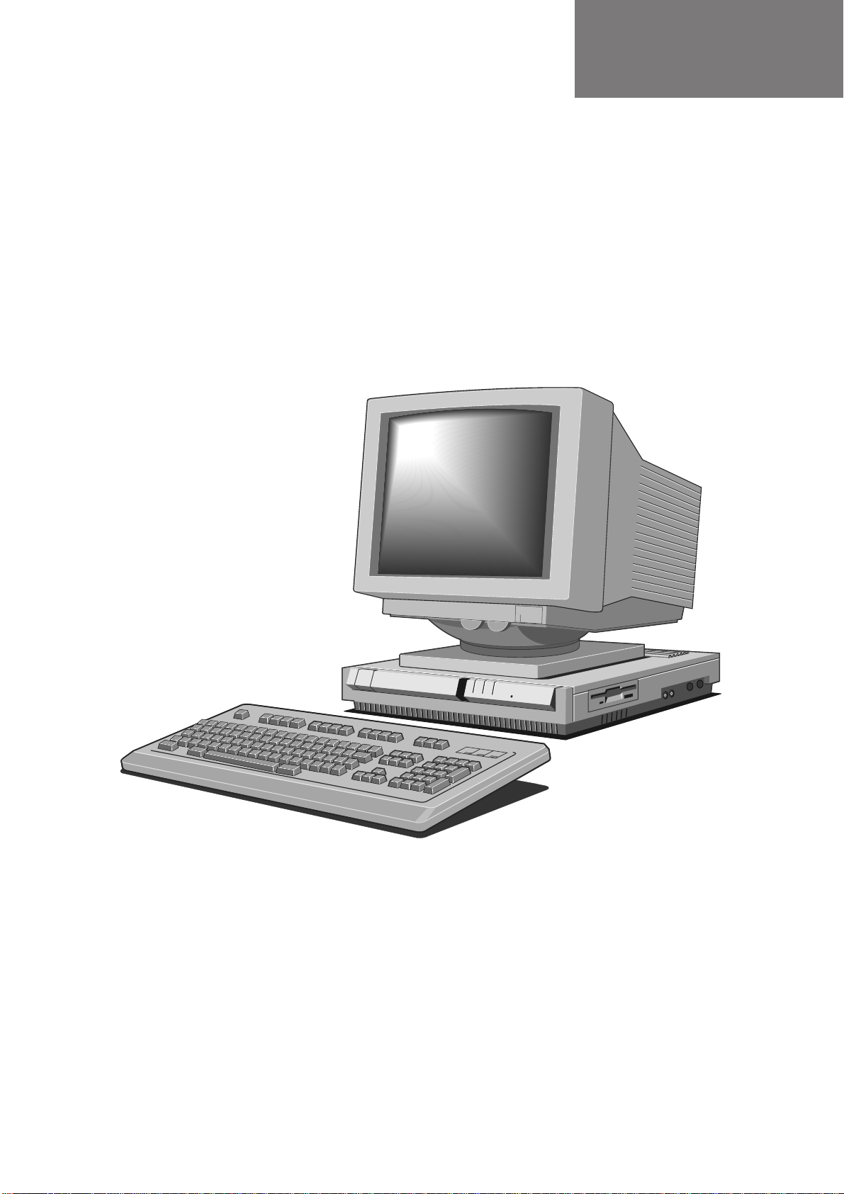
The Apricot LS Pro family is a range of ultra-compact IBM compatible computers which
can be used as a personal computer, a network workstation or a high resolution
graphics workstation.
The main features of the system are:
• 80386SX or 486SLC microprocessor operating at up to 33MHz.
• 2 to 16 Mbytes of on-board RAM.
• IBM compatible serial port.
• IBM compatible parallel port.
• Ethernet port.
• Token-Ring port (optional).
• PS/2 compatible mouse port.
• Floppy disk controller on system board.
• Hard disk connector on system board.
Chapter 3
Variants
Chapter 5Chapter 6 Chapter 3
• Full IBM functional compatibility.
• On-board VGA.
• On-board high resolution video.
• Internal power supply.
• LOC Technology security sub-system.
• Socket for 80387SX.
• Windows 3.1 compatible Business Audio subsystem.
The basic system unit may be fitted with:
• 2 to 16 Mbytes of RAM.
• 80, 120, 170, 240 or 540 Mbyte hard disk drive.
• 3.5 inch floppy disk drive.
• 80387SX coprocessor.
A VGA monitor will be required. To take advantage of the high resolution video modes
a suitable SVGA or EVGA monitor will be required.
1/2 LS PRO HARDWARE TECHNICAL REFERENCE

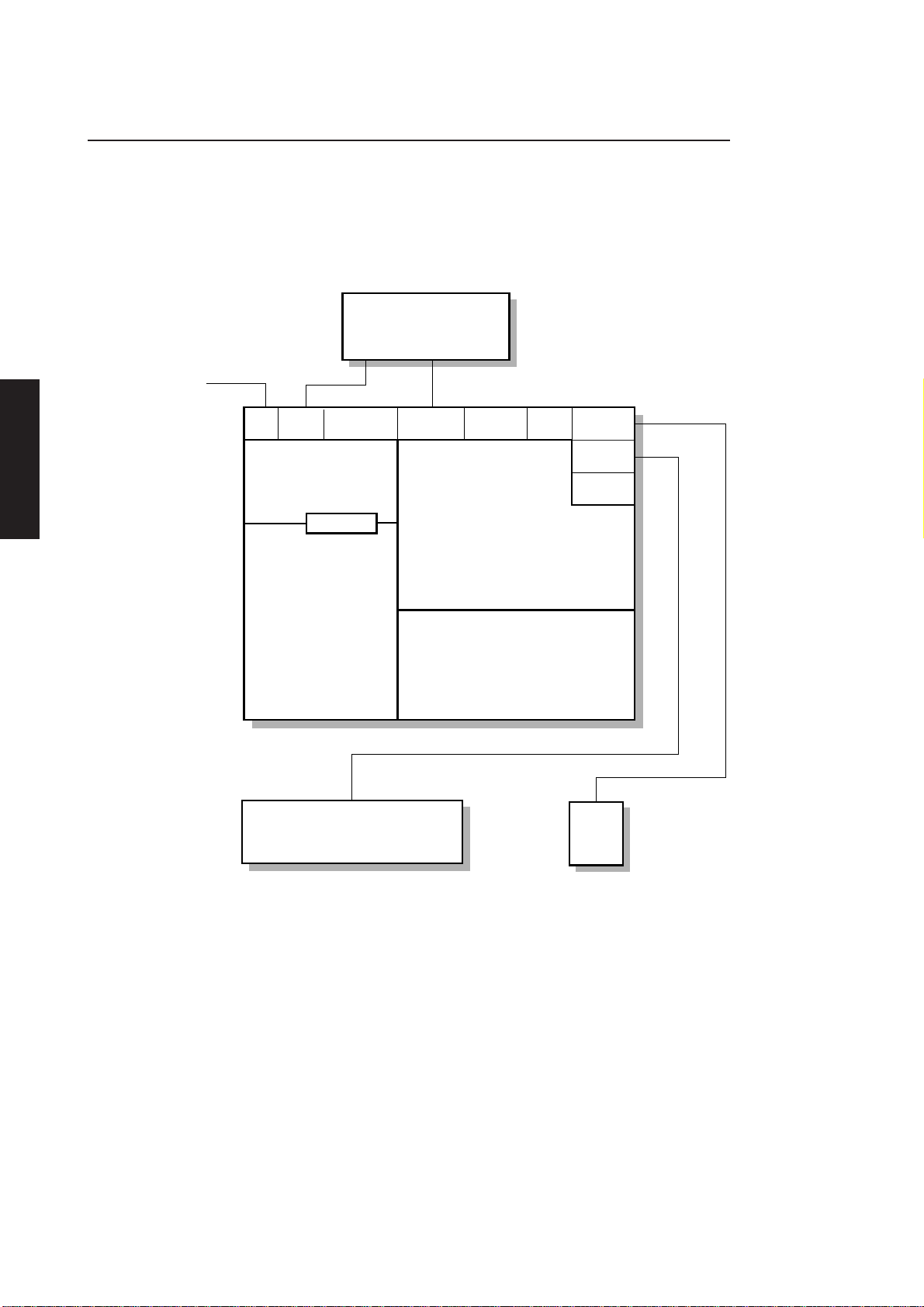
System unit
Introduction
The system unit contains: the processor(s), the system memory, disk drives, power
supply, security circuitry and interfaces to keyboard, monitor and peripherals. All the
interface circuitry except the Token-Ring network interface is on the system board.
Contents
Keyboard
Monitors
Dedicated connectors are provided on the system board for a Token-Ring module.
A block diagram of the system unit is shown at the end of this section. It shows the
components of the system and identifies functions implemented on the system board.
The keyboard is a full QWERTY typewriter keyboard and numeric keypad together
with editing keys. The layout of the 102 key UK keyboard is compatible with the IBM
AT enhanced keyboard.
The keyboard is fitted with a PS/2 style miniature DIN connector and any fully
compatible keyboard can be plugged into the system unit.
The system board is fitted, with a VGA video interface which will drive any suitable
monochrome or colour analogue monitor.
The on-board VGA controller also supports high resolution video modes. To take
advantage of the higher resolution video modes an SVGA or EVGA monitor must be
used. Video drivers for popular software packages are available.
Chapter 1
Chapter 1
Chapter 3
Chapter 3
Chapter 5
Chapter 6
LS PRO HARDWARE TECHNICAL REFERENCE 1/3
Introduction
Expansion
System RAM may be expanded to 16 Mbytes by fitting SIMMs.
Contents
Chapter 1
Chapter 1
A socket for an 80387SX coprocessor is fitted on the system board.
MONITOR
AC
INLETACOUTLET
POWER
SUPPLY
HARD DISK DRIVE
NETWORK
PORTS
FAN
VIDEO
PORT
PROCESSOR; MEMORY; VIDEO ADAPTER
ETHERNET CONTROLLER; SERIAL PORT
PARALLEL
PORT
SYSTEM BOARD
PARALLEL PORT;
LOC TECHNOLOGY SECURITY
FLOPPY DISK CONTROLLER;
HARD DISK CONNECTOR;
KEYBOARD AND MOUSE PORTS;
BUSINESS AUDIO.
FLOPPY DISK DRIVE
PORTS
including:
SERIAL
MOUSE
PORT
KEYBOARD
PORT
AUDIO
PORTS
Chapter 3
Chapter 5Chapter 6 Chapter 3
KEYBOARD
MOUSE
1/4 LS PRO HARDWARE TECHNICAL REFERENCE

SYSTEM UNIT
Chapter 2

Contents
2 SYSTEM UNIT
Introduction................................2/2
External layout...........................2/2
Internal layout ............................2/3
Servicing level.............................2/3
Dismantling and re-assembly . 2/3
Warnings and cautions........ 2/3
Antistatic precautions.......... 2/4
Equipment required ............. 2/4
System board connectors... 2/4
Removing the system unit top
cover ........................................2/5
Removing the system board
metalwork...............................2/6
Removing the floppy drive.. 2/7
Removing the power supply
metalwork...............................2/8
Removing the hard disk
drive..........................................2/9
Removing the fan................ 2/10
Removing the power
supply .................................... 2/11
Removing a Token-Ring
module .................................. 2/11
System unit
Removing a parallel port
cable ...................................... 2/13
Removing a thick wireEthernet
assembly ............................... 2/13
Removing the system
board ..................................... 2/13
Removing an escutcheon
plate....................................... 2/14
Removing the power switch
linkage ................................... 2/14
RFI screening tray and
insulation sheet ................... 2/15
Installing add-ons .................... 2/16
Memory upgrades............... 2/16
Installing an 80387SX......... 2/19
System unit connectors ........ 2/20
VGA....................................... 2/20
Ethernet................................ 2/20
Serial port............................. 2/21
Parallel port ......................... 2/22
Keyboard/mouse
connectors ........................... 2/22
Contents
Chapter 2
Chapter 2
Chapter 2
LS PRO HARDWARE TECHNICAL REFERENCE 2/1
Chapter 5
Chapter 6
System unit
Introduction
The main components of the system unit are:
Contents
Chapter 2
External layout
Chapter 2
• base
• top cover
• system board
• disk drives
• power supply
The top cover is easily removed without any tools.
The system board contains all the processing and interface circuitry and the system
RAM. 2 or 4 Mbytes of RAM is soldered to the board and SIMMs can be fitted to increase
the total amount of system RAM to a maximum of 16 Mbytes.
The front panel of the system unit contains: the power switch and slots for four LEDs
and the IR detector for the security card. The right side panel contains the keyboard
and mouse ports, and the audio input and output sockets.
POWER SWITCH
Chapter 2
Chapter 5
Chapter 6 Chapter 3
MOUSE
KEYBOARD
AUDIO IN
AUDIO OUT
INFRARED
SENSOR
LAN
INDICATOR
FLOPPY DISK
INDICATOR
HARD DISK
INDICATOR
POWER
INDICATOR
FLOPPY
DISK DRIVE
The floppy drive bezel is on the right side of the system unit.
The rear panel contains the following connectors: mains power input; auxiliary power
outlet; monitor; Ethernet ports; serial port; parallel port.
The layout of the rear panel is shown in the illustration below.
PARALLEL
PORT
SERIAL
PORT
SECURITY
LOOP
VIDEO
PORT
TWISTED
PAIR ETHERNET
THICK
ETHERNET/
TOKEN RING
PORT
COVER
LOCK
THIN
ETHERNET
PORT
POWER
OUT
POWER
IN
Illustrations and pinouts of the connectors on the rear panel are given at the rear of
this section.
2/2 LS PRO HARDWARE TECHNICAL REFERENCE
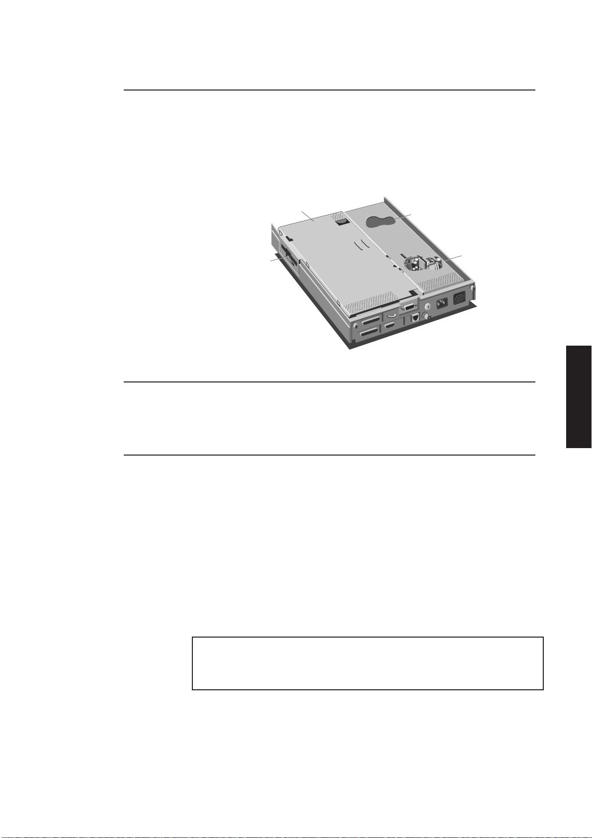
Internal layout
SYSTEM BOARD
METALWORK
FLOPPY
DRIVE
HARD DISK
DRIVE
POWER
SUPPLY
System unit
The layout of the inside of the system unit is shown in the illustration below. At the front
left of the system unit is the hard disk drive. Behind the hard disk drive is the power
supply unit. Both the power supply and the hard disk drive are beneath a metal cover.
Contents
Servicing level
The floppy drive is at the front right of the system unit attached to a metal plate which
extends the full length of the system board.
The level of information in this section is intended to enable suitably qualified personnel
to remove and replace major components of the system unit and to access components
to install add-ons.
Chapter 2
Chapter 2
Chapter 2
Dismantling and re-assembly
The LS Pro range has been designed to meet international EMI and safety standards.
Warnings and To ensure safety and continued compliance with these standards, observe the
cautions following precautions.
• It is recommended that modifications are carried out by an authorized dealer.
Unqualified users should not normally dismantle the equipment.
• Replacement parts should be of the type and rating specified by the manufacturer.
• All earth connections must be maintained to the original specification.
• Ensure that all personnel concerned are familiar with the action to be taken in
the event of electric shock.
Warning
Never carry out any work on the equipment with power applied. Always switch off at the mains
and remove the power lead from the equipment before starting work.
Note
Any reference to left or right during dismantling and re-assembly assumes that the reader is
viewing the unit from the front, unless otherwise stated.
Chapter 5
Chapter 6
LS PRO HARDWARE TECHNICAL REFERENCE 2/3
Contents
System unit
Antistatic All electronic components and equipments are sensitive to static electricity. Even
precautions small electrostatic discharges can render components useless or severely shorten
their working life, therefore preventive measures should always be taken.
No work should be carried on any item unless it is in a Special Handling Area (SHA)
as defined in BS CECC 00015:Part 1. In general this involves:
• a common earth point
• an earthed bench or bench mat
• an earthed wrist strap
Chapter 2
Chapter 2
Chapter 2
Equipment The following tools are required to dismantle the system unit.
required
• Philips screwdriver
• Flat-bladed screwdriver
• Nut spanner set
• thin nosed pliers
System board Many of the dismantling/reassembly procedures which follow involve the
connectors disconnection and reconnection of system board plugs and sockets. The following
table gives, for each socket, the connector number which identifies it. This number
is printed on the system board next to each connector.
Connector Label
Parallel port PL8
Token ring module PL9 and PL16
Hard disk drive power PL12
Thick Ethernet PL13
System board power PL15
Hard disk drive control PL17
Floppy disk drive PL18
Loudspeaker PL40
Chapter 5
Chapter 6 Chapter 3
2/4 LS PRO HARDWARE TECHNICAL REFERENCE
THICK
ETHERNET
ASSEMBLY
TOKEN RING
MODULE
SW 1
BATTERY
POWER
JUMPER
POWER
TOKEN RING
MODULE
System unit
PARALLEL
PORT
CABLE
Contents
Chapter 2
Chapter 2
HARD DISK
SIGNAL
FLOPPY
DISK
HARD DISK
POWER
LOUDSPEAKER
Removing the A keylock on the rear panel of the system unit locks the top cover in place. The
system unit cover cannot be removed unless this is unlocked. The cover is located by a ledge at
top cover the front and lugs on the sides and at the rear. Two thumbscrews in the rear panel
secure the cover.
Chapter 2
Chapter 5
LS PRO HARDWARE TECHNICAL REFERENCE 2/5
Chapter 6
System unit
The following illustration shows the thumbscrews and keylock.
Contents
Chapter 2
Chapter 2
CASING
SCREWS
COVER
LOCK
CASING
SCREWS
1. Check that the system unit power switch and mains supply are switched off and
disconnect the mains supply.
2. Ensure that the keylock on the rear panel is unlocked.
3. Loosen the two thumbscrews at the top of the rear panel. If they have been done
up tightly it may be necessary to use a screwdriver to loosen them.
4. Slide the top cover forward a few millimetres and lift it clear.
5. Replacing the top cover is simply the reverse of removal. Check that the keylock
is in the unlocked position. Make sure that the top cover is properly aligned
during replacement and do not force it into position.
Note
It is not necessary to remove cables (other than the mains power cable) to remove the system
unit top cover. However, in order to remove some of the internal components external cabling
must be removed.
Chapter 2
Chapter 5
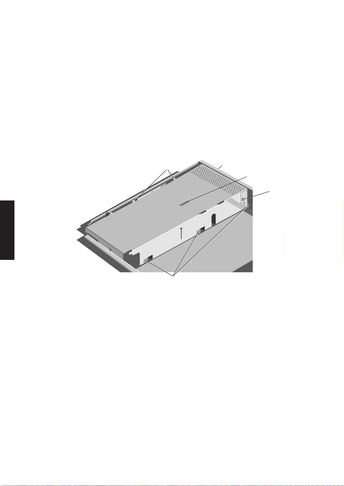
Removing the The system board metalwork is secured to the power supply metalwork by lugs, and
system board by clips to the system unit base.
metalwork
SECURING
LUGS
SECURING
CLIPS
1. Remove the system unit top cover.
2. Release the two retaining latches. On releasing the latches, the system board
metalwork will spring up slightly.
Chapter 6 Chapter 3
2/6 LS PRO HARDWARE TECHNICAL REFERENCE

System unit
3. Hinge the system board metalwork to the vertical as shown below:
4. Disconnect the loudspeaker cable from the system board.
5. If your system is fitted with a floppy disk drive disconnect the ribbon cable at the
system board taking care not to strain the cable or its connectors.
Contents
Chapter 2
Chapter 2
Chapter 2
6. Lift the system board metalwork clear of the computer.
7. Invert the system board metalwork, and rest it on a flat surface.
8. Replacement is simply the reverse of removal. Take care to ensure that the
metalwork engages correctly. Do not use undue force. Route the loudspeaker
cable between the front of the system unit and the LEDs.
Removing the The floppy drive is mounted in the metalwork above the system board.
floppy drive
Two variants of metalwork have been used, they are both shown in the illustration
below.
Chapter 5
Chapter 6
LS PRO HARDWARE TECHNICAL REFERENCE 2/7
System unit
1. Remove the system board metalwork.
2. Remove the four screws which secure the floppy drive and remove the drive.
Contents
Chapter 2
Chapter 2
3. Replacing the floppy drive is simply the reversal of removal. If the drive being
installed is a replacement ensure that the drive select switch on the side of the
drive is in the same position as that on the old drive.
Removing the The power supply metalwork covers the top of the power supply and divides the
power supply system unit, it applies gentle pressure to the top of the system unit fan. The system
metalwork board metalwork uses the power supply metalwork for location.
The power supply metalwork is secured by two screws and a number of lugs.
SECURING
SECURING
LUGS
SCREW
FAN LOCATION
SLOT
EARTH
BOND
SCREW
Chapter 2
Chapter 5Chapter 6 Chapter 3
SECURING
LUGS
1. Remove the system board metalwork.
2. Remove the earth bond screw which secures the system board escutcheon plate
to the power supply metalwork.
3. Remove the screw in the rear panel between the mains inlet and outlet which
secures the power supply metalwork.
4. Slide the power supply metalwork forward by approximately 6mm to free the
lugs.
5. An earth cable connects the power supply to the metalwork. Gently lift the
metalwork and carefully turn it over.
6. Remove the screw which secures the cable to the metalwork and lift the
metalwork clear.
2/8 LS PRO HARDWARE TECHNICAL REFERENCE

System unit
7. Replacement is the reverse of removal. However care must be taken to note the
following:
Warning
Contents
Remember to reconnect the power supply earth cable to the metalwork.
• The metalwork must be behind the switch operating lever of the power switch
linkage.
• A metal RFI screening tray is fitted in the base of the system unit. During the
replacement of the power supply metalwork the front edge of the tray can be
damaged.
In order to prevent damage occurring use a piece of card to hold down the
fingers at the front edge of the metalwork while the metalwork is replaced.
Once the metalwork is in place gently remove the card.
• Take care to ensure that the lugs on the bottom right of the metalwork are
properly engaged and that the metalwork does not foul on the fan.
The fan rests on a flexible foam pad which is compressed when the power
supply metalwork is in place. A slot is provided in the metalwork to allow a
small blunt instrument (flat bladed screwdriver) to push the fan down during
the replacement of the metalwork. Do not force the power supply metalwork
into position.
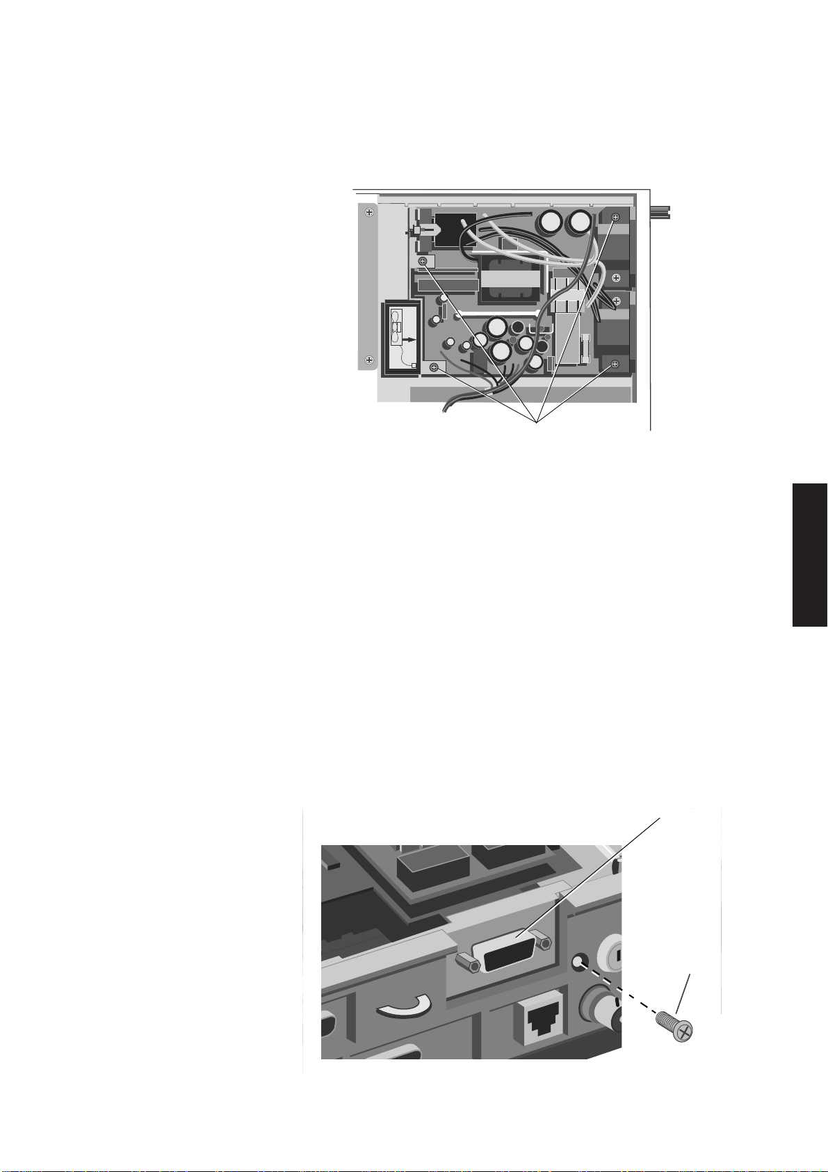
Removing the The hard disk drive is attached to the system unit base by four screws on the
hard disk drive underside of the system unit. The following illustration identifies the screws which
hold the hard disk drive in place.
Chapter 2
Chapter 2
Chapter 2
Chapter 3
HARD DISK
DRIVE
SECURING
SCREWS
1. Remove the system unit top cover, system board metalwork and power supply
metalwork.
2. Disconnect the hard disk drive power and signal cables from the system board.
Warning
Do not attempt to disconnect the cables from the drive with the drive still in the system
unit. Attempting to do so will damage the drive circuit board.
Chapter 5
Chapter 6
LS PRO HARDWARE TECHNICAL REFERENCE 2/9
System unit
Contents
Chapter 2
3. Holding the hard disk drive firmly in position carefully turn the system unit onto
one side and remove the four screws which secure it.
HARD DISK
DRIVE
Chapter 2
Chapter 2
Removing the fan The cooling fan rests on a flexible foam pad and is located in the base of the system unit
4. Still holding the disk drive, carefully turn the system unit back and rest it on the
work surface.
5. Slide the hard disk drive to the right to clear the power supply metalwork and
lift the hard disk drive out of the system unit complete with the power and signal
cables.
6. Replacing the hard disk drive is simply the reverse of removal. If the drive being
installed is a replacement ensure that the drive select jumpers are in the same
positions as those on the old drive.
Warning
1. Reconnect the power and signal cables to the drive before putting the drive in
position.
2. Ensure that the screws which you use to secure the drive are the ones which you
removed. If you use longer screws you will damage the drive.
by small ribs. Gentle pressure from the power supply metalwork ensures that the fan
is held in place.
1. Remove the power supply metalwork.
Chapter 5Chapter 6 Chapter 3
2/10 LS PRO HARDWARE TECHNICAL REFERENCE
2. Disconnect the fan power connector from the PSU.
3. Remove the fan.
4. Replacement is simply the reverse of removal. Make sure that you replace the
fan in the same orientation as it was before removal, and that the fan power cable
is secured to the fan with a cable tie.
System unit
SECURING
SCREWS
Removing the The power supply is secured to the bottom of the system unit by four screws. The
power supply following illustration identifies the screws that must be removed and the connectors
that must be disconnected in order to remove the power supply.
1. Remove the power supply metalwork.
Contents
Chapter 2
Chapter 2
2. Disconnect the system board and fan power connectors.
3. Lift out the fan.
4. Remove the four screws securing the power supply.
5. Lift the power supply clear of the system unit.
6. Replacement is simply the reverse of removal. Ensure that the voltage range
selection jumper is in the correct position for the mains supply available. The
jumper is identified in section 4 of this manual.
Removing a The Token-Ring module is secured to three standoff pillars inside the system unit,
Token-Ring and to the escutcheon plate at the rear of the system unit. To remove the module
module follow the instructions below:
1. Remove the system board metalwork.
2. Remove the screw in the rear panel of the system unit, to the right of the TokenRing connector.
TOKEN RING
CONNECTOR
Chapter 2
Chapter 3
Chapter 5
SECURING
SCREW
LS PRO HARDWARE TECHNICAL REFERENCE 2/11
Chapter 6
System unit
3. Remove the screws and nuts which secure the module to the standoff pillars.
Contents
Chapter 2
Chapter 2
SECURING
NUTS
4. Gently remove the module.
Note
Care must be taken to ensure that the module is removed vertically. Any horizontal
movement will damage the connectors.
SECURING
SCREW
Chapter 2
Chapter 5Chapter 6 Chapter 3
Read the following paragraphs before replacing the module.
The Token-Ring module connectors have three components: the connectors on the
system board, the connectors on the Token-Ring module, and the pin assemblies which
connect them. When you remove the Token-Ring module the pin assemblies will
probably come out with the Token-Ring module, although they may remain in the
system board.
When the Token-Ring module is in position the plate that surrounds the Token-Ring
connector is between the system unit base and the escutcheon plate. The two standoff
pillars by the connector nearest the power supply, protrude through corresponding
holes in the Token-Ring module.
It is vital that during replacement the Token-Ring module is correctly aligned. Any
misalignment will damage the connectors and/or the module. When replacing the
module make sure that the plate is inserted correctly and that the standoff pillars are
correctly aligned. Check that the connectors are correctly aligned, then gently insert
the module.
Warning
Take care not to exert undue pressure when inserting the module.
2/12 LS PRO HARDWARE TECHNICAL REFERENCE
System unit
Removing a The parallel port cable is secured to the escutcheon plate by the two D-type
parallel port connector screwlocks. To remove the cable:
cable
1. Remove the system board metalwork.
Contents
2. Remove the two screwlocks in the parallel port connector.
3. Unplug the cable from the socket on the system board and lift the cable clear.
4. Replacement is simply the reverse of removal.
Removing a thick The thick wire Ethernet assembly is secured to the escutcheon plate at the rear of
wire Ethernet the system unit. To remove the assembly follow the instructions below:
assembly
1. Remove the system board metalwork.
2. Remove the screw that secures the thick wire Ethernet assembly to the
escutcheon plate, unplug the assembly cable from the system board, and lift the
assembly clear of the system unit.
3. Replacement is simply the reverse of removal.
Removing the The system board is secured to the base of the system unit by seven screws through
system board the system board and four screwlocks through the escutcheon plate. The following
illustration identifies the positions of the system board screws.
SECURING SCREWS
Chapter 2
Chapter 2
Chapter 2
SECURING SCREWS
1. Remove the system unit top cover and put the system cover lock in the locked
position.
2. Remove the system board metalwork and disconnect all system board connectors.
3. Remove the parallel port cable and thick cable Ethernet assembly or Token-Ring
module (if fitted).
4. Remove the seven screws which secure the system board.
5. Remove the screwlocks that secure the video and serial port connectors.
6. Remove the lock nut on the thin Ethernet connector.
7. Carefully lift the system board clear of the system unit.
Chapter 3
Chapter 5
Chapter 6
LS PRO HARDWARE TECHNICAL REFERENCE 2/13

System unit
Contents
Chapter 2
escutcheon plate the rear of the system unit base. To remove the escutcheon plate:
Notes
1. If the system cover lock is not in the locked position the system board will foul during
removal.
2. During removal the audio connector may foul on the RFI isolation tray. If so, press
the isolation tray against the side of the system unit base to allow the connectors
clearance.
7. Replacement is simply the reverse of removal.
Ensure that all the switches and jumpers on a replacement board are in the correct
position.
Removing an The escutcheon plate at the rear of the system unit is secured by three screws to
1. Remove the system board metalwork.
2. Remove the system board.
Chapter 2
Chapter 2
3. Remove the screw that secures the escutcheon plate to the power supply
metalwork.
4. Remove the three screws that secure the escutcheon plate to the system unit,
and lift the escutcheon plate clear.
5. Replacement is simply the reverse of removal.
Removing the The power switch linkage mechanically links the system ON/OFF switch on the front
power switch of the system unit to the power supply ON/OFF switch. It is located in two slots in the
linkage system unit base plastics. The linkage must clear a rib on the side of the base plastics
during removal, and another during replacement. To remove the linkage:
REAR
SLOT
POWER SWITCH
LINKAGE
Chapter 5Chapter 6 Chapter 3
2/14 LS PRO HARDWARE TECHNICAL REFERENCE
FRONT
SLOT
SPRING
RIB
OPERATING
LEVER
1. Remove the system unit top cover, system board metalwork, hard disk drive,
power supply metalwork, fan, power supply and system board.
Warning
During the following instructions do not apply excessive pressure or the linkage may
be deformed or the plastics break.
System unit
2. Using a pair of thin nosed pliers, disconnect the spring and put it somewhere safe.
3. Exerting gentle inward pressure on the operating lever, slide the power switch
linkage forward past the rear of the two ribs, far enough to free the back of the
linkage from the rear slot.
Contents
4. Slide the linkage back bending it gently to allow it to pass to the right of the rear
slot and push it as far back as it will travel.
REAR
SLOT
OUTWARD
POWER SWITCH
LINKAGE
INWARD
SPRING
FRONT
SLOT
RIB
OPERATING
LEVER
5. With the 90° bend at the front of the linkage against the front of the two slots
swing the rear of the linkage into the centre of the system unit.
Chapter 2
Chapter 2
Chapter 2
Note
There should be no resistance to this movement. If there is resistance you have not
pushed the linkage far enough back.
6. Slide the linkage back through the slot and lift it clear.
7. Replacement is simply the reverse of removal except that gentle inward pressure
must be exerted to the front of the linkage to allow it to pass the front rib. Do
not force the linkage into place.
RFI screening tray The LS Pro system unit base is fitted with a metal RFI screening tray and a plastic
and insulation insulation sheet during manufacture. The metal tray reduces RFI emissions from the
sheet system unit and ensures compliance with international regulations.
The plastic sheet insulates components inside the system unit from the RFI
tray. Both components are essential.
There should never be any need to remove the tray or the screening sheet.
However if you do need to remove them you must ensure that they are
replaced correctly when you reassemble the system.
Chapter 3
Chapter 5
Chapter 6
LS PRO HARDWARE TECHNICAL REFERENCE 2/15
Contents
System unit
Insulation sheet
The plastic insulation sheet rests on the isolation tray and is not secured until the other
system unit components are installed. Correct positioning of the sheet can be ensured
by checking that the screw holes in the sheet align with those in the RFI tray, and the
system unit base.
RFI screening tray
The RFI screening tray sits in the system unit base, it is only secured by double sided
tape at the front left of the system unit, in front of the hard disk drive.
Chapter 2
Installing add-ons
Chapter 2
Chapter 2
Chapter 5Chapter 6 Chapter 3
Since the tray includes cut-outs for all the system unit connectors, the correct
orientation should be obvious. Ensure that the connector cut-outs and the screwholes
in the base of the tray are all correctly aligned with the system unit base. Then secure
the front left edge of the tray with the double-sided tape.
Memory During manufacture 2 or 4 Mbytes of RAM can be soldered to the system board.
upgrades System board memory can be expanded to a maximum capacity of 16 Mbytes by
fitting SIMMs in sockets provided on the system board.
When 4 Mbytes of RAM is installed during manufacture four SIMM sockets are fitted.
When 2 Mbytes of RAM is installed six SIMM sockets are fitted.
SIMMs must be installed in pairs, upgrades of 2 and 8 Mbytes are available. The 2 Mbyte
upgrade contains two 60nS 1Mx9 SIMMs, the 8 Mbyte upgrade contains two 60nS 4Mx9
SIMMs.
The following table identifies the valid upgrade combinations.
System board Upgrade
(Mbytes) (Mbytes)
2 4 2 - 2 6 2 2 2 8 2 2 2 1
2 12 2 8 2 16 - 8 8 2
4 6 N/A 2 4 8 N/A 2 2 1
4 12 N/A 8 4 16 N/A 8 8 2
1 2 3
Bank
Notecapacity to
Notes
1. For both system board RAM capacities an alternative method of achieving 8 Mbytes
of RAM is to install an 8 Mbyte upgrade in bank 2 and leave the other bank (or banks)
empty. This configuration disables the RAM soldered to the system board.
2. When banks 2 and 3 are both occupied by 8 Mbyte upgrades the RAM soldered to the
system board is disabled.
2/16 LS PRO HARDWARE TECHNICAL REFERENCE

System unit
The SIMM connectors are located on the right side of the system board just behind the
floppy drive bezel as shown in the following illustration.
SIMM SOCKETS
Note
Contents
Chapter 2
Chapter 2
When removing and installing SIMMs it is easiest to work with the rear of the system unit
towards you. As a result the following instructions assume that you are viewing the system unit
from the rear.
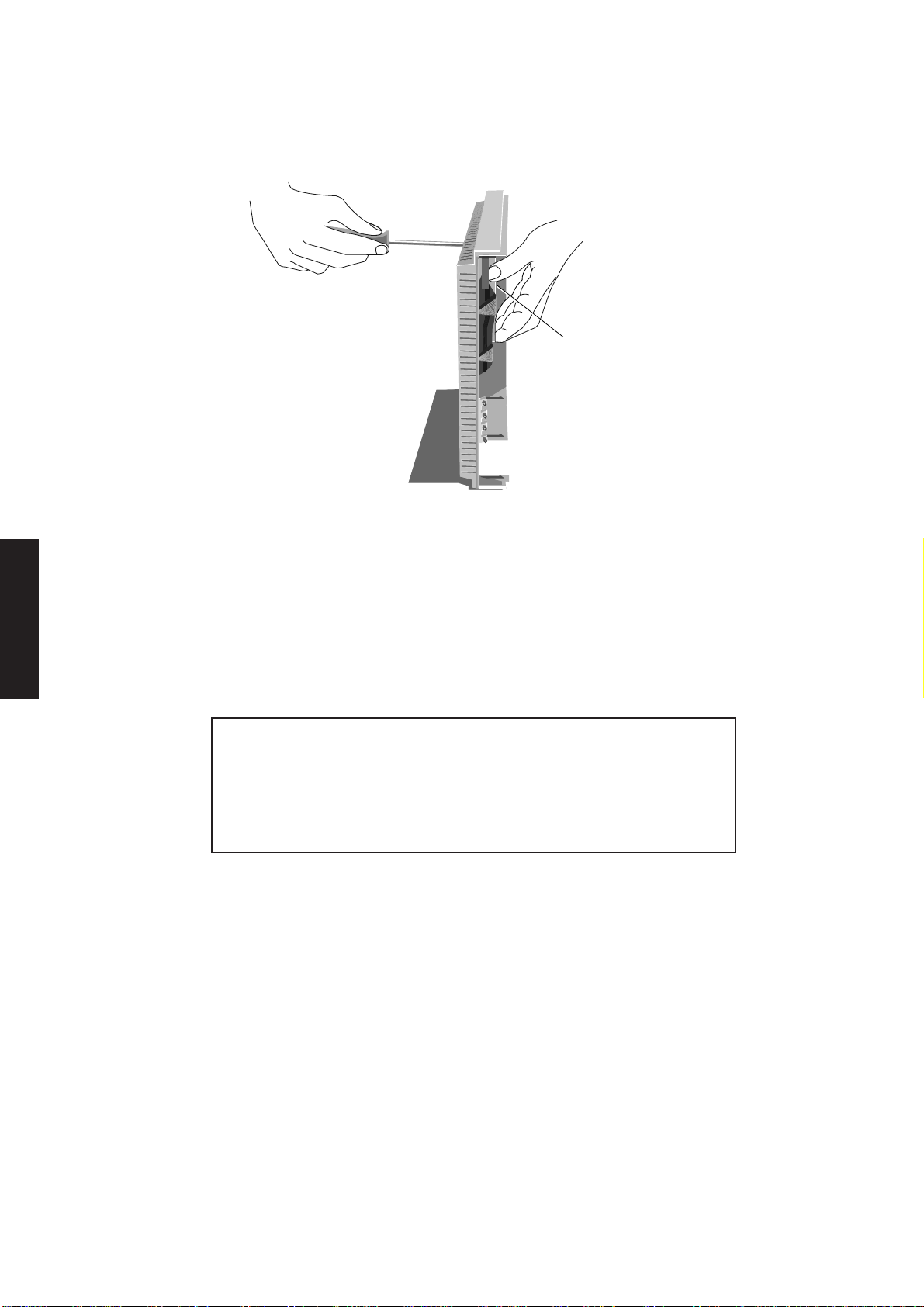
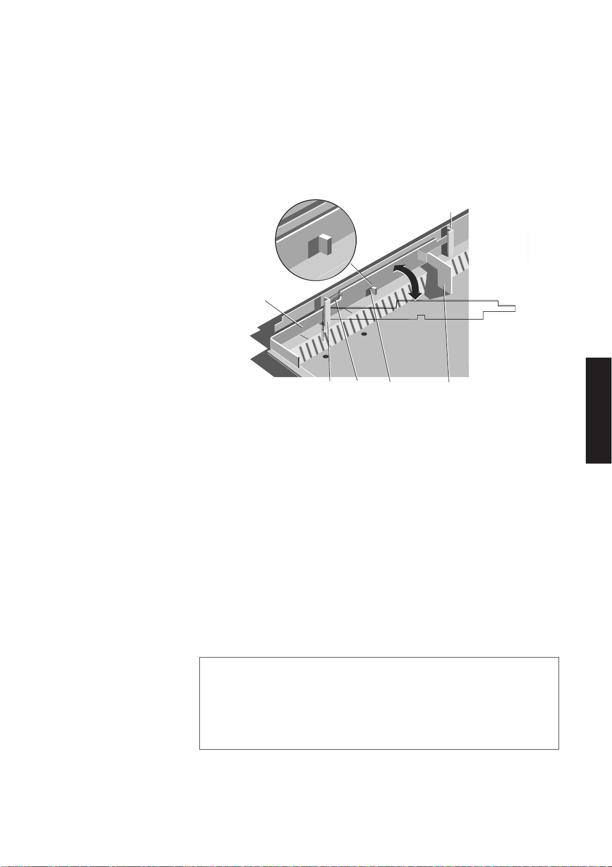
Removing SIMMs
If you wish to install an upgrade in a pair of SIMM sockets which are already occupied
you must first remove the existing SIMMs. Starting with the SIMM nearest the rear of
the system unit and working towards the front:
1. Lever the metal clips on each side of the socket gently away from the SIMM using
your thumbnails. When the clips are far enough apart the top edge of the SIMM
will move backwards until the SIMM is at an angle of about 15°.
Chapter 2
Chapter 3
Chapter 5
2. Taking care to avoid touching any of the components on the SIMM grip the top
corners of the SIMM between thumb and first finger and carefully pull the SIMM
out of the socket.
3. Repeat steps 1 and 2 for the other SIMM(s) affected.
LS PRO HARDWARE TECHNICAL REFERENCE 2/17
Chapter 6

System unit
Contents
Chapter 2
Chapter 2
Inserting SIMMs
From the illustrations showing the possible SIMM combinations decide which SIMM
capacity will be installed in each bank. Then, working from the socket nearest the front
of the system unit towards the rear, install the SIMMs.
To fit a SIMM:
1. Hold the SIMM so that the memory chips are facing the front of the system unit
with the metal connector strip nearest the system board.
2. Position the SIMM above the socket at an angle of about 15°.
Chapter 2
Chapter 5Chapter 6 Chapter 3
3. Lower the SIMM towards the socket. The right edge of the SIMM will be
prevented from reaching the connector by the securing clip.
4. Allow the left edge of the SIMM to drop into the connector.
5. Push the SIMM gently to the right and lower the right edge into the connector.
6. Ensure that the SIMM is properly located in the connector.
7. Rotate the SIMM into the vertical position by pushing gently on the top corners.
8. If the SIMM is properly located the SIMM should remain in position held by the
securing clips, and with a small plastic lug through the holes on either side of the
SIMM.
2/18 LS PRO HARDWARE TECHNICAL REFERENCE

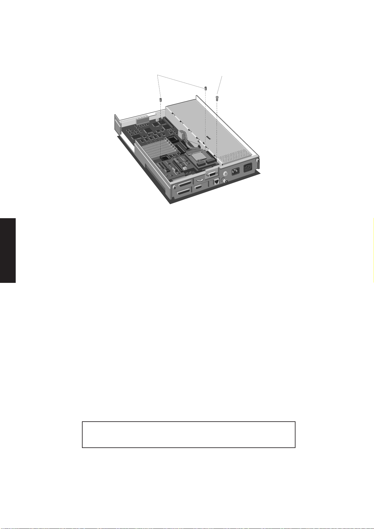
Installing an 1. Remove the system unit top cover.
80387SX
2. Remove the system board metalwork.
3. Locate the 80387SX socket from the following illustration.
PIN 1
80387SX
SOCKET
4. The 80387SX has a positioning guide in the form of a circular recess. Insert the
80387SX in the socket with the positioning guide at pin 1 making sure that you
do not bend or otherwise damage the pins.
System unit
Contents
Chapter 2
Chapter 2
Chapter 2
Note
The 80387SX only fits in one orientation. Do not use excessive force or damage may
occur.
5. Reassemble the system.
Chapter 3
Chapter 5
Chapter 6
LS PRO HARDWARE TECHNICAL REFERENCE 2/19

Contents
System unit
System unit connectors
The following illustrations and tables show the layout, pin numbering and pinout of each
of the connectors on the rear panel of the system unit.
5
1
Chapter 2
Chapter 2
Chapter 2
VGA The VGA display connector is a 15-pin D-shell.
Pin I/O Output Mono Colour
1 O Red No pin Red
2 O Green Mono Green
3 O Blue No pin Blue
4 NA Reserved No pin No pin
5 NA Digital Gnd Self Test Self Test
6 NA Red rtn Key pin Red rtn
7 NA Green rtn Mono rtn Green rtn
8 NA Blue rtn No pin Blue rtn
9 NA Plug No pin No pin
10 NA Digital Gnd Digital Gnd Digital Gnd
11 NA Reserved No pin Digital Gnd
12 NA Reserved Digital Gnd No pin
13 O Hsync Hsync Hsync
14 O Vsync Vsync Vsync
15 NA Reserved No pin No pin
10
6
1115
Chapter 5Chapter 6 Chapter 3
Ethernet Thick
The thick Ethernet connector is a 15-pin female D-shell
which uses a slide to hold the male and female connectors
together.
Pin I/O Signal
1 NA Collision presence shield
2 I Collision presence (+ve)
3 O Transmit (+ve)
4 NA Receive shield
5 I Receive (+ve)
6 NA Power return
7 NA Reserved (+ve)
8 NA Reserved shield
9 I Collision presence (-ve)
10 O Transmit (-ve)
11 NA Transmit shield
12 I Receive (-ve)
13 NA Power
14 NA Power shield
15 NA Reserved (-ve)
8
15
1
9
2/20 LS PRO HARDWARE TECHNICAL REFERENCE

System unit
Thin
The thin Ethernet connector is a BNC socket.
Core Signal
Shield Return
Twisted pair (TPE)
The unshielded twisted-pair Ethernet port is an RJ45 connector.
Pin Function
1 Transmit data +
2 Transmit data 3 Receive data +
4 Not used
5 Not used
6 Receive data 7 Not used
8 Not used
1 2 3
1
Contents
Chapter 2
4
5
6
7
8
Chapter 2
Chapter 2
13
Serial The serial port uses a male 25-pin D-shell
connector.
Pin I/O Signal name
2 O Transmit data (COM1)
3 I Receive data (COM1)
4 O Request to send (COM1)
5 I Clear to send (COM1)
6 I Data set ready (COM1)
7 NA Signal ground
8 I Data carrier detect (COM1)
12 I Data carrier detect (COM2)
13 I Clear to send (COM2)
14 O Transmit data (COM2)
16 I Receive data (COM2)
19 O Request to send (COM2)
20 O Data terminal ready (COM1)
22 I Ring indicate(COM1)
All other pins are not connected.
Note
14
25
Chapter 3
Chapter 5
Chapter 6
The Rev C system board does not provide the COM2 signals.
LS PRO HARDWARE TECHNICAL REFERENCE 2/21

System unit
Contents
Chapter 2
Chapter 2
Parallel port The parallel port uses a female 25-pin D-shell
connector.
Pin I/O Signal name Pin I/O Signal name
1 I/O Strobe 14 O Autofeed XT2 I/O Data bit 0 15 I Error3 I/O Data bit 1 16 O Init4 I/O Data bit 2 17 O Slct In5 I/O Data bit 3 18 NA Ground
6 I/O Data bit 4 19 NA Ground
7 I/O Data bit 5 20 NA Ground
8 I/O Data bit 6 21 NA Ground
9 I/O Data bit 7 22 NA Ground
10 I Ack- 23 NA Ground
11 I Busy 24 NA Ground
12 I PE 25 NA Ground
13 I SLCT
13 1
25
14
Keyboard/mouse The keyboard and mouse connectors are miniature 6-pin
Chapter 2
Chapter 5Chapter 6 Chapter 3
connectors DIN connectors.
Pin I/O Signal name
1 I/O Data
2 NA Reserved
3 NA Ground
4 NA +5Vdc
5 I/O Clock
6 NA Reserved
6
5
4
3
2 1
2/22 LS PRO HARDWARE TECHNICAL REFERENCE

SYSTEM BOARD
Chapter 3

Contents
3 SYSTEM BOARD
System Board
Contents
3.1 Introduction ............................3/2
General...................................... 3/2
System Identification Number
(SIN).......................................3/2
Major components............3/2
Description.............................. 3/4
Coprocessor.......................3/4
System reset........................3/4
3.2 Processor system ................3/5
80386SX processor features.3/5
486SLC processor features.3/5
Address and data bus
structure................................... 3/5
Software compatibility ........3/5
Modes of operation..............3/5
3.3 SCAMP ...................................3/6
Memory controller........... 3/6
System control port B.....3/6
Interrupt structure ...............3/6
List of hardware interrupts 3/7
Non-Maskable Interrupts3/8
Direct Memory Access.......3/8
Address generation ..........3/8
System timers .........................3/9
Operation.............................3/9
3.4 System memory .................3/10
General................................... 3/10
Read only memory (ROM) .. 3/10
Random access memory
(RAM)..................................... 3/10
Real time clock (RTC)RAM. 3/11
Contents of RTC RAM.... 3/11
3.5 Video adapter .....................3/14
General................................... 3/14
Video controllers ........... 3/15
3.6 Floppy disk controller .......3/15
General................................... 3/15
Drive formats ...................... 3/15
3.7 Hard disk interface ............3/16
General................................... 3/16
Interface signal descriptions 3/16
3.8 Peripherals controller .......3/17
Serial ports............................ 3/17
Programmable baud-rate
generator........................... 3/17
Parallel port.......................... 3/18
3.9 Keyboard/mouse
controller ............................3/18
General................................... 3/18
Keyboard password security. 3/18
3.10 LOC Technology ................3/19
3.11 Ethernet port .......................3/19
General................................... 3/19
82596 LAN coprocessor.. 3/20
82C503 dual serial
transceiver ........................ 3/20
7997..................................... 3/20
3.12 Apricot Business Audio ....3/21
3.13 System board connectors..3/21
Hard disk drive connectors. 3/21
Control Connector....... 3/21
Power connector ........... 3/22
Floppy drive connector ... 3/22
System board power
connector.............................. 3/22
Battery jumper .................... 3/22
Chapter 1
Chapter 2
Chapter 3
Chapter 3
Chapter 5
LS PRO HARDWARE TECHNICAL REFERENCE 3/1
Chapter 6

System Board
3.1 INTRODUCTION
General
ContentsChapter 1
This section describes the LS Pro system board and the operation of its processing
system and interface circuits.
The LS Pro range uses a highly integrated, IBM AT compatible system board. In addition
to standard features, the LS Pro system board provides: Ethernet interface, business
audio subsystem, LOC Technology security subsystem and a mouse port.
System Each system board fitted with the LOC Technology subsystem is identified by its own
Identification System Identification Number (SIN). During normal operation the SIN will never be
Number (SIN) required. Under certain circumstances the system may display a prompt asking for the
SIN to be entered. If this happens refer to the Owner's Handbook and associated
documentation. If Apricot’s LOC Technology software is in use refer to the
documentation supplied with the software.
Chapter 2
Chapter 3
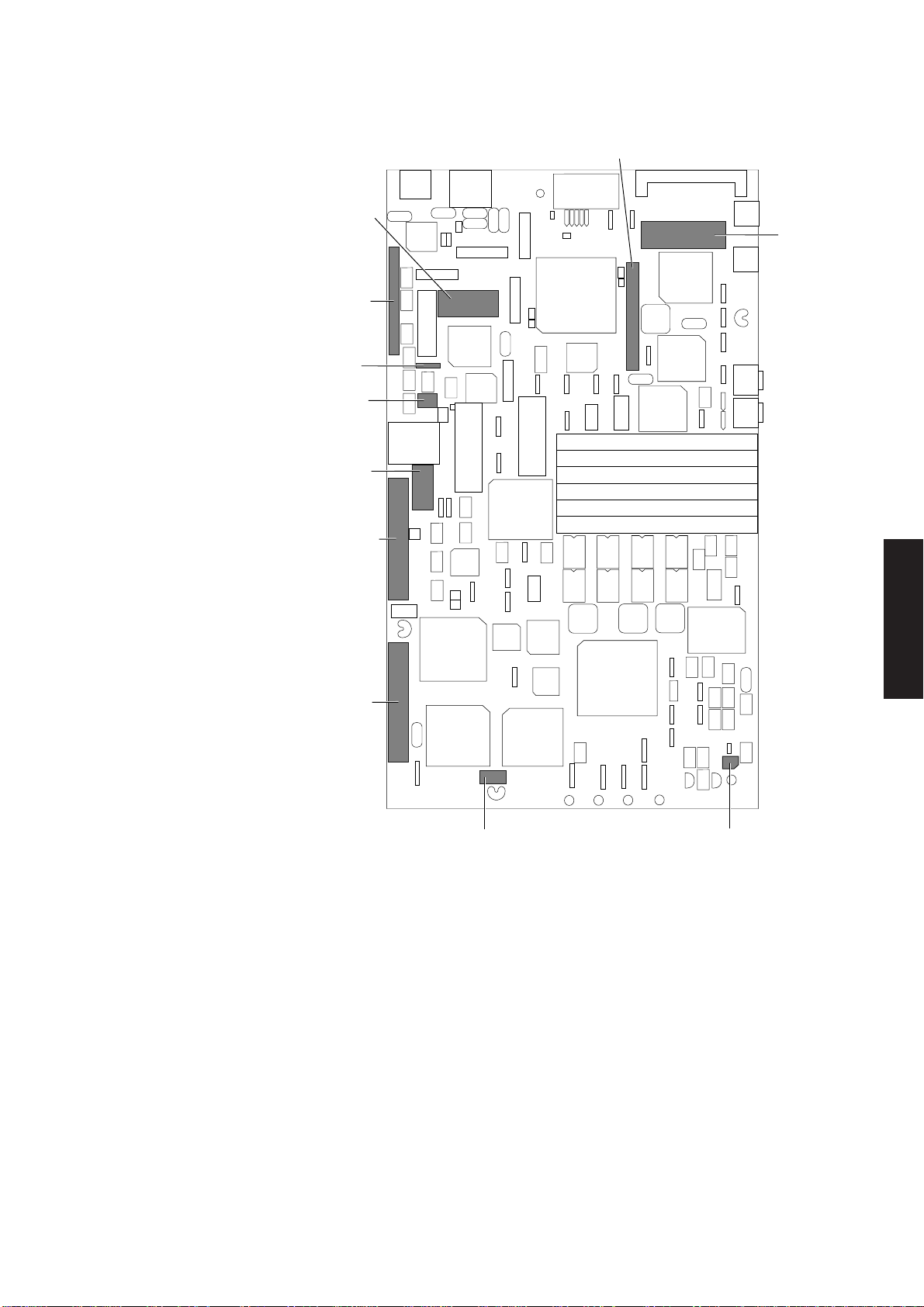
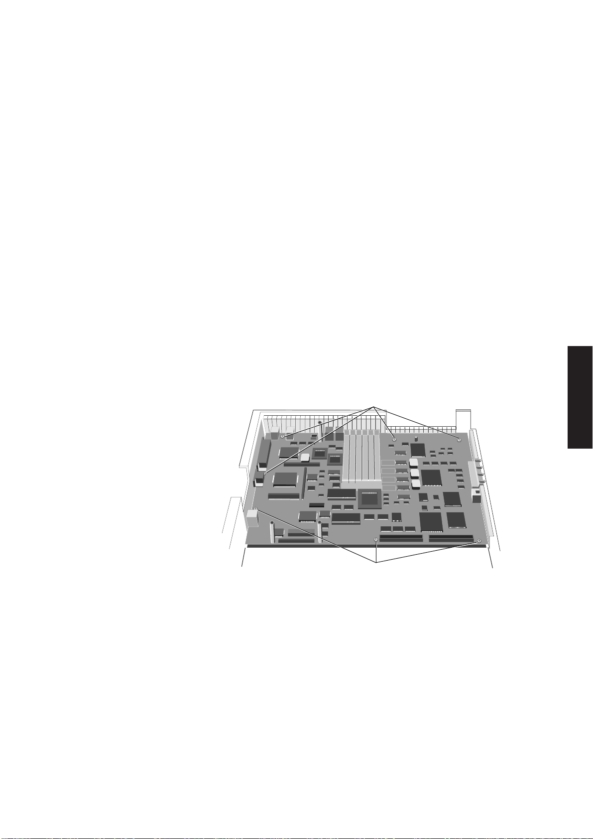
Major The following list of major components on the system board identifies the custom chips
components and briefly details their function:
1. Processor: 80386SX
486SLC
2. 4 Mbytes of RAM
3. 128 Kbyte ROM
4. VL82C311 (SCAMP) AT chipset
5. 8042 keyboard and mouse interface
6. CL-GD542X video controller with 1Mbyte of video RAM
7. 82596SX based Ethernet interface
8. 8051 based LOC Technology security feature
9. ATA compatible hard disk interface
10.82077 based floppy drive interface
11.16C452 based serial and parallel ports
12.Four SIMM sockets for memory expansion
Chapter 5Chapter 6 Chapter 3
3/2 LS PRO HARDWARE TECHNICAL REFERENCE
13.146818A Real Time Clock
14.Yamaha YMZ263 based business audio subsystem

System Board
TOKEN RING
MODULE
CONNECTOR
PARALLEL
PORT
SOCKET
PERIPHERALS
CONTROLLER
KEYBOARD
CONTROLLER
TOKEN RING
MODULE
CONNECTOR
THICK
ETHERNET
SOCKET
POWER
CONNECTOR
SIMM
SOCKETS
R A M
80387SX
SOCKET
ETHERNET
CONTROLLER
SCAMP
AUDIO
PROCESSOR
FLOPPY
CONTROLLER
HARD DISK DRIVE
CONNECTOR
FLOPPY
CONNECTOR
ROM BIOS
BATTERY
VIDEO
CONTROLLER
The major components are identified in the following illustration.
Contents
Chapter 1
Chapter 2
Chapter 3
Chapter 3
Chapter 5
Chapter 6
LS PRO HARDWARE TECHNICAL REFERENCE 3/3
System Board
Description
ContentsChapter 1
The following description of the system board should be read in conjunction with the
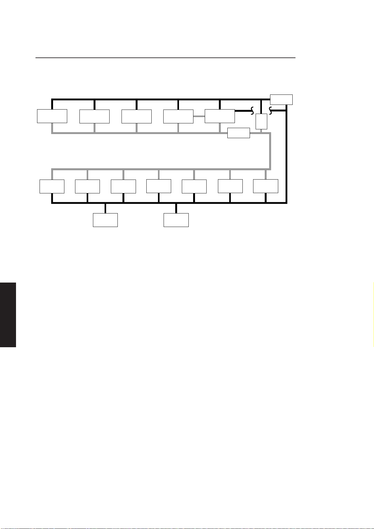
block diagram below. The diagram shows the peripheral areas of circuitry which are
connected to the CPU. For clarity, timing and control signals are omitted.
Chapter 2
Chapter 3
80387SX
TOKEN RING
MODULE
CONNECTORS
PROCESSOR
IDE
CONNECTOR
LOCAL DATA 0-15
LOCAL ADDRESS 0-23
KEYBOARD
MOUSE
CONTROL
ETHERNET MEMORY
FLOPPY
CONTROL
PERIPHERAL
CONTROL
REAL
TIME
CLOCK
AUDIO
MA
SCAMP
82C311
LA
SYSTEM ADDRESS 0-23
VGA
LD
BUFFER
BIOS
ROM
SA
EXPANSION
ROM
SYSTEM DATA 0-15
BUFFER
The block diagram is a functional description of the system board and does not identify
specific chips.
The LS Pro system board uses highly integrated components, reducing the chip count
and the system board area, and increasing reliability. The VLSI SCAMP chipset
integrates much of the standard AT system board peripheral logic onto a single chip.
SD
Chapter 5Chapter 6 Chapter 3
The processor and coprocessor are connected to a 16-bit local bus running at 33MHz.
Control logic for the local bus is integrated in SCAMP.
Memory addresses are generated by SCAMP and are routed to system memory on a
dedicated memory address bus. Memory data uses the local data bus.
The 82596 based Ethernet interface connects directly to the local bus allowing fast
transfers to and from system memory.
The BIOS ROM is addressed from the system bus and places its data on the local bus.
All other peripheral circuitry is connected to the system bus.
Coprocessor The system board includes a socket for an 80387SX coprocessor. This is a high
performance numeric coprocessor which further improves the performance of the
processing system in applications which perform many floating point arithmetic
operations.
The coprocessor has two I/O ports 00F0h and 00F1h which are used to control reset
and error latching. The coprocessor interface control logic is integrated in SCAMP.
If a coprocessor is fitted on the system board it should always be reset at the same time
as the processor.
System reset The system is automatically reset on power up. No external hardware reset facility is
provided. Some operating systems provide a software reset e.g. MS-DOS resets the
machine if CTRL, ALT and DEL are pressed at the same time.
3/4 LS PRO HARDWARE TECHNICAL REFERENCE

3.2 PROCESSOR SYSTEM
The processor system uses either an 80386SX or a 486SLC microprocessor, these are
described below.
System Board
Contents
80386SX The 80386SX is a high performance microprocessor which features:
processor
features • 24-bit address and 16-bit data busses.
• compatibility with software written for less powerful members of the 80X86
microprocessor family - the 8086, 8088 and 80286.
• high speed.
• enhanced modes of operation - real, protected and virtual 8086 mode.
• on board memory management unit.
486SLC The 486SLC incorporates all the features of the 80386SX listed above. In addition
processor it offers:
features
• 1 Kbyte of cache RAM.
• 80486SX instruction set compatibility.
Address and data bus structure
The system board utilises all address and data lines available on the processor. This
allows up to 16 Mbytes of physical memory to be addressed.
Chapter 1
Chapter 2
Chapter 3
The total addressable I/O space of the processor is 64 Kbytes. Section 5 shows how
it is used and details the I/O ports used by various devices.
Software compatibility
Existing software which has been written for the 8086/8088/80286 will be executed at
greater speed on the 80386SX/486SLC, even higher performance will be achieved with
new software which takes advantage of the 80386SX or 486SLC architecture and
enhanced instruction set.
Modes of operation
The processor enters real mode at power up or when it is reset. In this mode it provides
fast execution in an unprotected mode like that of the 8086 or 80286 in real mode. The
main difference between the 80386SX/486SLC, and the 80286/8086 in this mode is
speed.
In the protected mode the 80386SX/486SLC has all the advanced architectural features
of the 80286: memory management and protection mechanisms, task management, and
virtual memory support. In addition it operates with greater speed and supports 32bit registers and instructions.
In the virtual 8086 mode the 80386SX/486SLC creates one or more 8086 environments
within its protected multitask environment. This allows multiple 8086 tasks or a
mixture of 8086 and 80286/80386 tasks to be executed concurrently.
Chapter 3
Chapter 5
Chapter 6
LS PRO HARDWARE TECHNICAL REFERENCE 3/5

System Board
3.3 SCAMP
ContentsChapter 1
The LS Pro system board is based on a VLSI VL82C311 single chip AT
compatible chipset. The VL82C311 integrates the following standard AT
system board peripheral logic in a single QFP package:
• two 8237A DMA controllers
• two 82C59A interrupt controllers
• 82C54 system timer
• 74LS612 memory mapper
• 82284 clock generator and ready interface
• 82288 bus controller
In addition to the logic listed above the VL82C311 also includes:
• memory controller
Chapter 2
Chapter 3
Interrupt structure
• bus steering logic
• parity generation and checking logic
• Port B and NMI logic
Memory The memory controller integrated in the VL82C311 can access the full 16Mbyte
controller address range of the processor. Memory is addressed in up to four banks of 2 or 8
Mbytes. Page mode operation and interleaving maximise system performance.
Full LIM 4.0 support is included with 36 mapping registers. ROM shadowing is
supported from 640k to 1M.
System control Port B is located at I/O location 0061h. The port may be used for: gate timer 2 (speaker);
port B speaker data; RAM parity check enable; enable I/O channel check; refresh detect; timer
2 out; I/O channel check; RAM parity check. The detailed function of each bit is
described in section 5.
The system board supports 16 levels of edge sensitive, maskable hardware
interrupts, including Non-Maskable Interrupts (NMI).
Chapter 5Chapter 6 Chapter 3
3/6 LS PRO HARDWARE TECHNICAL REFERENCE
The interrupt control circuitry is functionally equivalent to two 8259A
programmable interrupt controllers. Each controller has eight interrupt inputs;
one interrupt input is used to cascade the controllers together. This leaves
fifteen inputs available for the processing system to use.
The output from the controllers goes to the INTR input on the processor. All
of the interrupts may be masked using the processor CLI instruction.

System Board
The following illustration shows the maskable interrupt structure.
Contents
IRQ0
IRQ1
IRQ3
IRQ4
IRQ5
IRQ6
IRQ7
IRQ8
IRQ9
IRQ10
IRQ11
IRQ12
IRQ13
IRQ14
IRQ15
0
INTA
1
2
3
D0 to D7
4
5
6
RD,WR
7
MASTER
CONTROLLER
0
INTA
1
2
D0 to D7
3
RD,WR
4
5
6
7
SLAVE
CONTROLLER
INT
XD0 to XD7
A0
INT
A0
IOR, IOW
SA0
INTR
INTA
8-BIT
DATA
BUS
ADDRESS
BUS
List of hardware The interrupts are allocated to hardware functions in the priorities shown in the
interrupts following table. IRQ0 is the highest priority.
Chapter 1
Chapter 2
Chapter 3
Interrupt level Function
IRQ0 Timer
IRQ1 Keyboard
IRQ2 Slave controller input
IRQ8 Real time clock
IRQ9 Token ring module
IRQ10 Ethernet port
IRQ11 Security
IRQ12 Mouse
IRQ13 Coprocessor exception
IRQ14 Hard disk controller
IRQ15 Digital audio
IRQ3 Reserved
IRQ4 Serial port
IRQ5 Reserved
IRQ6 Floppy disk controller
IRQ7 Parallel port
Note
Chapter 3
Chapter 5
Chapter 6
IRQ0 and IRQ13 are both used inside the SCAMP chip. Neither emerges for use on the system
board.
LS PRO HARDWARE TECHNICAL REFERENCE 3/7

System Board
ContentsChapter 1
Direct Memory Access
Chapter 2
Non-Maskable A non-maskable interrupt (NMI) is generated in the event of a parity or I/O error.
Interrupts Reading Port B indicates the source of the NMI. NMI may be disabled by writing to
I/O address 0070h.
On power up, and after a reset the NMI bit of port 0070h is set to 1 (NMI
disabled). Before NMI is enabled after a power up the I/O channel check state
is initialized by POST.
Note
I/O port 0070h is also used to access the Real Time Clock CMOS RAM, as a result port 0071h
must be read immediately after port 0070h has been written to enabling or disabling NMI.
If this is not done the successful operation of the Real Time Clock and its CMOS RAM cannot
be guaranteed.
Direct Memory Access (DMA) allows data to be transferred to or from system
memory without interrupting the system processor. The DMA controller is
functionally equivalent to two 8237A DMA controllers.
Chapter 3
Chapter 5Chapter 6 Chapter 3
The DMA controller may be programmed by the system microprocessor. The
DMA registers are programmed or read by the system processor addressing
the DMA controller in the ranges shown below.
• hex 0000 to 001F
• hex 0081 to 008F
• hex 00C0 to 00DF
Details on the effect and usage of these addresses is given in section 5.
The two 8237A compatible controllers are cascaded with the DREQ and
DACK signals of channel 0 on one controller connected to the HRQ and HLDA
signals of the other controller. This arrangement results in four 8-bit DMA
channels (DMA1) and three 16-bit channels (DMA2).
The table below shows which DMA channels are allocated which functions.
DMA channels 0 and 1 support memory-to-memory transfers.
DMA channel Function
1 Audio
2 Floppy drive interface
3 Audio
Address In order to access the full 16Mbyte address space of the processor the DMA controller
generation must generate a 24-bit address. The bits 0-7 are taken directly from the 8237A address
outputs, bits 8-15 are latched from the 8237A data outputs while bits 16-24 are from
the appropriate DMA page register.
3/8 LS PRO HARDWARE TECHNICAL REFERENCE

System timers
System Board
The SCAMP chip provides a three channel 82C54 compatible system timer.
The counters are:
Contents
counter 0 system timer
counter 1 refresh request
counter 2 sound output
Full details on the operation of 8254 counters are given in the manufacturers
data sheets and are not repeated here.
The system timers are programmed by accessing the four I/O ports recognised
by the timers. The counters provide six modes of operation. The four I/O ports
which are used to program the counters are organised as one count register
for each counter and one control byte (I/O ports 0040h to 0043h). The function
of each port is given in section 5.
Operation The clock input to the timer is 1.193 MHz. This is obtained by dividing the14.31818 MHz
system oscillator (OSC) by twelve. The output frequency of each timer is then
separately programmed by loading the associated count register.
System timer
BIOS loads the counter 0 registers with a value of 65536 which results in a
system timer frequency of approximately 18.2Hz. The output of counter 0
generates a hardware interrupt, IRQ0, which is used to maintain a time of day
clock based on the number of “ticks” since midnight.
Chapter 1
Chapter 2
Chapter 3
Chapter 3
Refresh request
The BIOS loads the counter 1 registers with a value of 18 which generates a
refresh request rate of 66.278kHz (one refresh request every 15.08 µseconds).
A refresh request puts the processor into hold and accesses memory via a DMA
type operation.
Sound output
The sound output may be set to give the output frequency required. To enable
the output bit 0 of Port B (I/O 0061h) must be set to 1.
Chapter 5
Chapter 6
LS PRO HARDWARE TECHNICAL REFERENCE 3/9

System Board
3.4 SYSTEM MEMORY
General
ContentsChapter 1
Read only memory (ROM)
Chapter 2
Random access memory (RAM)
Chapter 3
The system board contains:
• 128 Kbytes of ROM.
• system RAM.
• 50 byte battery backed Real-time clock CMOS RAM.
• expansion ROM socket (optional).
The system ROM contains the BIOS and the system board Setup utility. It
consists of a 1 Mbit EPROM arranged as 128 Kbytes of memory. It is addressed
at the top of the first and last Megabyte of the processor address space and is
not parity checked.
The lower 64 Kbytes of the ROM contains code which is used only during the
boot process. If shadow RAM is enabled this lower 64 Kbyte address space
(E0000-EFFFF) is available for use as RAM. If shadowing is disabled the top 128
Kbytes of the first and last Mbytes are used by the system ROM.
Four Megabytes of RAM are soldered directly to the system board. Additional
RAM is plugged into SIMM sockets on the system board. Upgrades are in pairs
of 1 or 4 Mbyte SIMMs giving upgrade capacities of 2 and 8 Mbytes. The
following table gives the permissible upgrade combinations and the total system
RAM available with each.
Chapter 5Chapter 6 Chapter 3
System board
capacity (Mbytes)
4 6 N/A 2 4 8 N/A 2 2
4 12 N/A 8 -
4 16 N/A 8 8
Note
When banks 2 and 3 are both occupied by 8 Mbyte upgrades the RAM soldered to the system
board is disabled.
Upgrade to
(Mbytes)
1 2 3
Bank
(Mbytes)
3/10 LS PRO HARDWARE TECHNICAL REFERENCE

Real time clock (RTC) RAM
The real time clock and its associated battery backed RAM is an MC146818. The RTC
RAM is accessed via I/O ports 0070h and 0071h. The first fourteen bytes are used to
store real time clock information, the remainder are used for system configuration
data.
The RTC is normally powered from the system +5V supply. However when the
computer is not switched on power is supplied by a rechargeable battery on
the system board. This maintains the correct time and configuration information.
If the battery becomes discharged the time and date will need to be reset and
the system will need to be reconfigured using the SETUP utility.
System Board
Contents
Chapter 1
Contents of The contents of the RTC RAM are listed below.
RTC RAM
Address Function Address Function
Real time clock data 16 Base memory (high byte)
00h seconds 17
01h alarm seconds 18
02h minutes 19 Drive type for hard drive 0
03h alarm minutes 1A-1E Reserved
04h hours 1F shadow BIOS
05h alarm hours 20-27 Reserved
06h day of week 28 Apricot sound volume
07h date 29 Apricot options
08h month 2A Apricot boot type
09h year 2B
0Ah status register A 2C-2D Reserved
0Bh status register B 2E High byte checksum for 10-2D
Chapter 2
Expected expanded memory
(low byte)
Expected expanded memory
(high byte)
Chapter 3
Chapter 3
Apricot cache disable
(see also byte 34h)
0Ch status register C 2F Low byte checksum for 10-2D
0Dh status register D 30
0E Diagnostic Status 31
0F Shutdown code 32 Century in BCD
Configuration data 33
10 Diskette drive type 34
11 Reserved 35 Apricot access rights
12 Fixed disk drive type 36 Floppy/Token-Ring autodetect
13 Power on password 37 Hard disk autodetect
14 Equipment byte 38-3E Power on password
15 Base memory (low byte) 3F Byte checksum of bytes 38-3E
LS PRO HARDWARE TECHNICAL REFERENCE 3/11
Actual expanded memory
(low byte)
Actual expanded memory
(high byte)
Memory exceeds 512K/387
presence
486SLC cache control
(see also Apricot byte 2Bh)
Chapter 5
Chapter 6

System Board
The contents of each of the RTC RAM locations which requires further explanation
is described in the following table.
ContentsChapter 1
Chapter 2
Chapter 3
Chapter 5Chapter 6 Chapter 3
Location/Title Bit(s) Function
0E 7 1 = Real time clock lost power
Diagnostic 6 1 = CMOS checksum bad
status 5 1 = Invalid configuration at POST
4 1 = Memory size error at POST
3 1 = Fixed disk fails initialization
2 1 = CMOS time found invalid
1, 0 Reserved
0F 7-0 00h = Normal execution of POST
Shutdown 01h = Chipset initialization for real mode re-entry.
code 05h = Issue an EOI and JMP to 40:67h
06h = JMP to 40:67h without an EOI
07h = Return to INT 15h function AH=87h block move
08h = Return to POST memory test
09h = Return to INT 15h function AH=87h block move
0Ah = JMP to 40:67h without an EOI
10 7-4 Drive type of diskette drive 0
Diskette 0000 = No drive
drive type 0001 = Not used (360k)
0010 = Not used (1.2MB)
0011 = Not used (720k)
0100 = 1.44MB
0101-1111 are Reserved
3-0 Reserved (no second drive)
12 7-4 Drive type for drive 0 (0-14) if 15 look at byte 19h
Fixed disk 3-0 Reserved
drive type
13 7-1 Reserved
Power on 0 1 = Power on password enabled
password
14 7-6 Diskette drives installed
Equipment 00h = 1
byte 01-03h Reserved
5-4 Primary display adapter
00h = VGA
01h = Not used (40 column colour)
02h = Not used (80 column colour)
03h = Not used (Monochrome)
3-2 Reserved
1 1 = 80387 installed
0 1 = Diskette drive available for boot
3/12 LS PRO HARDWARE TECHNICAL REFERENCE

System Board
Location/Title Bit(s) Function
1F 7-4 Reserved
Shadow BIOS 3 1 = shadow BIOS
2-0 Reserved
28 7-0 Sound volume 0 = minimum, FF = maximum
Sound volume
29 7 1 = Power on sound enabled
Options 6 1 = Quiet boot (No text output)
5 1 = Fast boot
4-3 Reserved
2 1 = Graphical boot
1-0 Monitor type
00 = VGA
01 = HiVision 14"
10 = HiVision Low Emission
11 = Reserved
2A 7 Token-Ring Bus width (see 36h bit 1)
Boot type 1 = 16-bit, 0 = 8-bit
6 Token-Ring data rate
0 = 16 Mbits/sec, 1 = 4 Mbits/sec
5 1 = Token-Ring present
4-3 Reserved
2-0 Remote Boot type
000 = None
001 = Ethernet RPL
010 = Token-Ring RPL
100 = Optional ROM at C000
2B 7-0 00h = Cache enabled
Cache disable CDh = Cache disabled (see 34h)
33 7 1 = memory exceeds 512K
RAM exceeds 6-5 Reserved
512K/387 status 4 Save 387 status
1 = present, 0 = not present
3-0 Reserved
34 7-6 Reserved
486SLC cache 5 1 = cache enabled (see 2Bh)
4-0 Reserved
35 7-2 Reserved
Access rights 1 1 = Setup access right enabled
0 1 = Floppy boot right enabled
36 7-2 Reserved
Floppy/ 1 1 = Token-Ring present
Token-Ring 0 1 = Floppy drive present
autodetect
Contents
Chapter 1
Chapter 2
Chapter 3
Chapter 3
Chapter 5
Chapter 6
LS PRO HARDWARE TECHNICAL REFERENCE 3/13

System Board
3.5 VIDEO ADAPTER
General
ContentsChapter 1
Chapter 2
Chapter 3
Chapter 5Chapter 6 Chapter 3
The video adapter on the LS Pro system board is based on either a Cirrus Logic
CL-GD5422 or 5426 chip. These chips contain all the elements of a VGA controller,
except display memory, providing 100% compatibility with the IBM VGA standard.
The video controller consists of the GD542X, 1 Mbyte of display memory and a 7.6mA
current reference. Video dot clocks vary from 25 to 65 MHz depending on video mode.
Software support is provided by a video BIOS included in the system BIOS.
In addition to full compatibility with the VGA standard the video controllers support
a range of enhanced video modes.
The video modes available are given in the following table:
Mode Type Colours
0, 1 Text 16/256K 40x25 9x16 360x400
2, 3 Text 16/256K 80x25 9x16 720x400
4, 5 Graphics 4/256K 40x25 8x8 320x200
6 Graphics 2/256K 80x25 8x8 640x200
7 Text - 80x25 9x16 720x400
D Graphics 16/256K 40x25 8x8 320x200
E Graphics 16/256K 80x25 8x8 640x200
F Graphics - 80x25 8x14 640x350
10 Graphics 16/256K 80x25 8x14 640x350
11 Graphics 2/256K 80x30 8x16 640x480
12 Graphics 16/256K 80x30 8x16 640x480
13 Graphics 256/256K 40x25 8x8 320x200
58 Graphics 16/256K 100x37 8x16 800x600
5C Graphics 256/256K 100x37 8x16 800x600
5D Graphics 16/256K 128x48 8x16 1024x768
5F Graphics 256/256K 80x30 8x16 640x480
60 Graphics 256/256K 128x48 8x16 1024x768
64 Graphics 64K - - 640x480
65 Graphics 64K - - 800x600
66 Graphics 32K - - 640x480
67 Graphics 32K - - 800x600
6C Graphics 16/256K 160x64 8x16 1280x1024
6F Graphics 64K 40x25 8x8 320x200
70 Graphics 16M 40x25 8x8 320x200
71 Graphics 16M 80x30 8x16 640x480
Displayed
Chars
Character
Cell
Pixels
Note
Mode 6C is interlaced only.
Sync signals output to the monitor are at TTL levels while the analogue video
outputs are at 0 to 0.7 volts.
3/14 LS PRO HARDWARE TECHNICAL REFERENCE

System Board
Video controllers The video controllers implement all the control and data registers, and all the data
manipulation capabilities and data paths of the standard VGA controller. In addition
they can generate high-resolution display modes (those supported in BIOS are
listed in the table above), and uses several enhancements to improve on the
performance of the standard VGA implementation.
These enhancements include a pair of FIFOs. One isolates the processor from
display memory, allowing zero wait state writes from processor to display
memory, provided the FIFO is not full. Reads also occur with zero wait states
provided the data required is held in the FIFO. The second allows the use of
fast page mode cycles to fetch data from display memory, increasing the time
that the display memory is available for processor accesses.
In addition the GD5426 includes a hardware BitBLT which accelerates video
performance under GUIs.
3.6 FLOPPY DISK CONTROLLER
General
The diskette drive controller fitted on the system board is an Intel 82077 chip.
This single chip provides a complete IBM compatible floppy disk controller,
including data separator, on a single chip.
Contents
Chapter 1
Chapter 2
Chapter 3
Drive formats
The controller has several internal registers which are accessible by the system
microprocessor. These registers, and their usage, are described in detail in
section 5. An illustration and pinout of the floppy drive connector are given at
the rear of this section.
The controller supports:
• two drives
• 500 kbyte unformatted media, 360 kbyte formatted
• 1 Mbyte unformatted media, 720 kbyte formatted
• 1.66 Mbyte unformatted media, 1.2 Mbyte formatted
• 2 Mbyte unformatted media, 1.44 Mbyte formatted
• supports 250, 300 and 500 kbits/sec transfer rates
• programmable precompensation delay
In this implementation a single 1.44 Mbyte floppy drive can be fitted. 720k and
1.44M diskettes are supported for both single and multithread operations. The
default precompensation is 125 nanoseconds and is present for all cylinders.
Chapter 3
Chapter 5
Chapter 6
LS PRO HARDWARE TECHNICAL REFERENCE 3/15

System Board
3.7 HARD DISK INTERFACE
General
ContentsChapter 1
Interface signal descriptions
Chapter 2
The hard disk drive connector which is fitted on the LS Pro system board is an
IDE connector which conforms to the ATA interface standard.
The hard disk drive is accessed via a group of I/O ports at 01F0-01F7h. The
function of each port is given in section 5.
The connector is buffered from the system bus by bi-directional transceivers.
A pinout of this and the hard disk drive power connector is given at the rear
of this section.
Host reset
Reset signal to the drive. Active low during system power up.
Host data 0-15
Chapter 3
Chapter 5Chapter 6 Chapter 3
16-bit bi-directional data bus between the system board and the drive.
Host I/O channel ready
This line allows the drive to lengthen I/O read and write cycles by generating
system board wait states. The signal is normally high and is driven low by the
drive if an I/O cycle is to be lengthened.
Host IOW
Write strobe. This signal clocks data from the system board to the drive on the
data bus.
Host IOR
Read strobe. This signal clocks data from the drive to the system board on the
data bus.
Host IRQ14
This is the interrupt signal from the drive. This signal is active high when the
drive is selected and the drive interrupt enable bit (IEN) is activated by the
system board. An interrupt is cleared when the drive receives the next
command, when the drive status register is read, or when the drive is reset.
Host IOCS16
Informs the system board that the drive data register has been enabled and the
drive is prepared to perform a 16-bit I/O transfer.
Host ADDR 0-2
These lines are used to select registers on the drive.
3/16 LS PRO HARDWARE TECHNICAL REFERENCE

3.8 PERIPHERALS CONTROLLER
A 16C452 peripherals controller provides two serial and one parallel port.
Serial ports
The serial controllers integrated in the 16C452 are fully compatible with the
NS16450 serial communications controller. They automatically add and remove
start, stop and parity bits. Programmable baud rate generators allow operation
from 50 baud to 56 Kbaud. The ports support 5, 6, 7 and 8-bit characters with
1, 1.5 or 2 stop bits. A prioritized interrupt system controls transmit, receive,
error and line status as well as data-set interrupt.
Each serial port controller provides the following functions:
System Board
Contents
Chapter 1
• Full double buffering in character mode
• False start-bit detection
• Line-break generation and detection
• Modem control functions:
Clear to send (CTS)
Request to send (RTS)
Data set ready (DSR)
Ring indicator (RI)
Data carrier detect (DCD)
Note
The DSR, DTR and RI modem control signals of COM2 do not appear on the serial port at
the rear of the system unit.
COM1 is connected to the system address and data busses using IRQ4 while
COM2 uses IRQ3. The controllers occupy a group of eight consecutive I/O
ports COM1 at 03F8-03FFh and COM2 at 02F8-02FFh. The ports have the
following significance.
Location Significance
0 Transmit Data
Receive Data
Baud Rate Generator Divisor (Low byte)
1 Baud Rate Generator Divisor (High byte)
Interrupt Enable
2 Interrupt Identification Register
3 Line Control Register
4 Modem control Register
5 Line Status Register
6 Modem Status Register
7 Scratch Pad Register
Chapter 2
Chapter 3
Chapter 3
Chapter 5
Chapter 6
Programmable The serial port controllers each contain a programmable baud-rate generator
baud-rate which can divide the clock input (1.8432 MHz) by any divisor from 1 to 65,535. The
generator output frequency of the baud-rate generator is the baud-rate multiplied by 16. Two
8-bit latches store the divisor in a 16-bit binary format. These divisor latches must
be loaded during setup to ensure the correct operation of the baud-rate generator.
When either of the divisor latches is loaded, a 16-bit baud counter is immediately
loaded. This prevents long counts on the first load.
LS PRO HARDWARE TECHNICAL REFERENCE 3/17

System Board
Parallel port
ContentsChapter 1
Chapter 2
3.9 KEYBOARD/MOUSE CONTROLLER
The parallel port is fully compatible with the IBM AT parallel port. The port is
output only and allows the attachment of peripherals that accept parallel data
at standard TTL levels.
A pinout and illustration of parallel port 25-pin D-shell connector is given at the
rear of section 2.
The parallel port is accessed via the three I/O ports given in the following table.
Address R/W Function
03BCh r/w Data register
03BDh read Status register
03BEh write Control register
These registers control the operation of the parallel port. They are described
in detail in section 5.
General
Chapter 3
Keyboard password security
Chapter 5Chapter 6 Chapter 3
The keyboard and mouse interfaces are implemented on the system board on
an Intel 8042 chip. The keyboard connector on the system unit is dedicated to
that function, the mouse connector can be used for any auxiliary device with
a serial interface compatible with the 8042. Illustrations and pinouts of these
connectors are at the rear of section 2.
The 8042 receives the serial data, checks the parity, translates the keyboard
scan codes and presents the data to the system as a byte of data at data port
I/O address 0060h. The interface can interrupt the system when data is available
or can wait for polling from the microprocessor.
I/O address 0064h is the command/status port. When the system reads port
0064h it receives status information from the 8042. When the system writes
to the port, the 8042 interprets the byte as a command.
The significance of port 0064h is described in section 5.
The 8042 provides a password security mechanism. Three commands are
available regarding password operation:
A4 Test Password Installed
A5 Load Security
A6 Enable Security
3/18 LS PRO HARDWARE TECHNICAL REFERENCE

System Board
The system microprocessor may determine if a password is currently installed with a
Test Password Installed command. This allows a controlling program to decide
whether or not to overwrite an existing password.
The system microprocessor may set a password in the 8042 at any time with a Load
Security command. Any existing password is lost, and the new password becomes the
active password. The password must be installed in scan code format.
The system microprocessor places the system in secure mode with the Enable Security
command. In secure mode the 8042 does not pass any information to the system
microprocessor. The 8042 intercepts the keyboard data stream and continuously
compares it with the installed password pattern. No keyboard or auxiliary device data
is passed to the system microprocessor until a match is found. When a match occurs
the 8042 is restored to its previous state and data is passed to the system microprocessor.
There is no limit to the number of times the password may be changed. No command
is available to verify the installed password. The 8042 accepts no commands when
keyboard security is active.
Contents
Chapter 1
Chapter 2
3.10 LOC TECHNOLOGY
The system board is fitted with a LOC Technology security subsystem. This subsystem
allows Apricot LOC Technology software to control access to data and facilities.
When Apricot LOC Technology is not in use the security hardware is passive and has
no effect on the system.
3.11 ETHERNET PORT
General
The Ethernet port on the system board is based around an 82596 Local Area Network
Coprocessor, an 82C503 Dual Serial Transceiver and an AMD7997. This provides a
port which complies fully with the IEEE 802.3, 10BASE5, 10BASE2 and 10BASET
specifications.
The coprocessor and dual serial transceiver make up an Ethernet controller for thick
cabling, and with an additional analog filter module a TPE controller. The 7997
interfaces between the thick and thin Ethernet cabling standards.
An expansion ROM socket may be fitted to the system board. This socket is intended
to allow for alternative remote boot ROMs. The system BIOS includes RPL remote
boot code.
Chapter 3
Chapter 3
Chapter 5
Chapter 6
The Ethernet standard defines a requirement for every device to have a unique address.
This is implemented in a PROM on the system board.
LS PRO HARDWARE TECHNICAL REFERENCE 3/19

System Board
The Ethernet port occupies a group of 17 I/O ports. The ports have the following
significance:
ContentsChapter 1
Chapter 2
Location (Hex) Significance
0 Port
1-3 Reserved
4 CA
5-7 Reserved
8-D Ethernet Address
E Reserved
F Checksum
10 Status register
82596 LAN The 82596 is connected to the processor local bus. The 82596 is an intelligent co-
coprocessor processor which performs many network control tasks.
The inherent intelligence of the 82596 reduces host processor overhead, and allows
all time critical functions to be performed independently of the host. This along with
the inherent speed of the processor local bus results in a high performance network
interface, with minimum host processor overhead.
The host processor monitors and controls the 82596 through a shared memory
structure known as the System Control Block (SCB). The 82596 uses the HOLD and
HOLDA signals to gain control of the local bus in order to access the SCB.
Chapter 3
serial transceiver to interface the 82596 to an AUI port and a TPE network. In addition to the normal
Chapter 5Chapter 6 Chapter 3
Both the 82596 and the host can modify the SCB. The processor uses the Channel
Attention (CA) line to notify a change to the 82596, while the 82596 generates a
hardware interrupt if it has modified the SCB.
The host can communicate with the 82596 via a single port (PORT). This allows the
host to, amongst other things, reset the 82596.
Full details on the 82596 and its operation are given in the manufacturers data sheets.
82C503 dual The 82503 dual serial transceiver (DST) incorporates all the active circuitry necessary
features of an IEEE 802.3 transceiver the 82503 also incorporates automatic port
selection, and polarity switching.
Automatic port selection selects either TPE or the AUI port without external
intervention. If a good TPE connection is available the 82503 will select the TPE port,
if no TPE connection is available the AUI port will be selected.
Note
The thin cable Ethernet port is derived from the AUI port. To select thick or thin Ethernet, SW1
must be in the correct position.
Automatic polarity selection allows the 82503 to overcome the most common wiring
problem on TPE networks. If the polarity of the receive signal pair is reversed as a result
of a crossed pair of wires, the 82503 automatically corrects the error by reversing the
signals internally.
7997 The Ethernet transceiver chip acts as the interface between thick and thin Ethernet
cabling standards, implementing the IEEE802.3 10BASE2 standard.
3/20 LS PRO HARDWARE TECHNICAL REFERENCE

3.12 APRICOT BUSINESS AUDIO
The Apricot Business Audio subsystem integrated on the LS Pro system board
is based on a Yamaha YMZ263 chip. It offers two channels each of which can
be independently configured to either playback or record.
Each channel incorporates a PCM/ADPCM encoder/decoder, 12-bit ADC and
DAC and a 128 byte FIFO. In PCM mode the maximum sample rate is 44.1kHz,
in ADPCM it is 22.05kHz.
The digital audio subsystem uses DMA channel 1 to transfer data to and from
audio channel 0 and DMA channel 3 for audio channel 1.
System Board
Contents
Chapter 1
The YMZ263 occupies a block of eight ports from 388-38Fh. A description of
the operation of this block of ports is included section 5.
3.13 SYSTEM BOARD CONNECTORS
Hard disk drive connectors
Control Connector
Pin Function Pin Function
1 host reset- 21 2 ground 22 ground
3 host data 7 23 host IOW4 host data 8 24 ground
5 host data 6 25 host IOR6 host data 9 26 ground
7 host data 5 27 host I/O channel ready-
8 host data 10 28 -
9 host data 4 29 reserved
10 host data 11 30 ground
11 host data 3 31 host IRQ14
12 host data 12 32 host IOCS16-
13 host data 2 33 host ADDR1
14 host data 13 34 15 host data 1 35 host ADDR0
16 host data 14 36 host ADDR2
17 host data 0 37 -
18 host data 15 38 19 ground 39 20 key 40 ground
Chapter 2
Chapter 3
Chapter 3
Chapter 5
Chapter 6
The pin layout of the connector.
LS PRO HARDWARE TECHNICAL REFERENCE 3/21
2
1
40
39

System Board
Power connector
ContentsChapter 1
Floppy drive connector
Chapter 2
Pin Function
1 +12 Volts
2 ground (for +12V)
3 ground (for +5V)
4 +5 Volts
Pin Function Pin Function
2 density select 1 14 drive select 2
3 not connected 16 motor on
4 not connected 18 direction
5 5V 20 step
6 density select 0 22 write data
7 5V 24 write enable
8 index 26 track 00
9 5V 28 write protect
10 drive select 0 30 read data
11 5V 32 head select
12 drive select 1 34 disk change
1234
Chapter 3
Chapter 5Chapter 6 Chapter 3
System board power connector
Battery jumper
Note
All other pins are connected to 0 Volts.
2
1
34
33
Pin Function
1 +12V
2 +12V
3 +5V
4 +5V
5 0V
10
5
6
1
6 0V
7 0V
8 0V
9 -12V
10 Power good
A two position jumper is provided alongside the system board battery. With the
jumper in the position away from the power supply metalwork the battery provides
power to the system board maintaining the contents of CMOS RAM and powering the
Real time clock when mains power is not available.
If the jumper is moved to the position nearest the power supply metalwork battery
power to the system board is disconnected, and the CMOS RAM is discharged.
The jumper is identified in the illustration on page 2/5, and instructions on accessing
the system board are given in section 2.
3/22 LS PRO HARDWARE TECHNICAL REFERENCE

PERIPHERAL ITEMS
Chapter 4

Contents
Peripheral items
Preface
4 PERIPHERAL ITEMS
4.1 Power supply ...........................4/2
Description .................................4/2
Connector ..................................4/3
4.2 Monitors .....................................4/3
Introduction................................4/3
Maintenance................................4/4
Video signal.................................4/4
Apricot SVGA colour
monitor........................................4/4
External controls .................. 4/4
HiVision Low Emission
14" colour ...................................4/6
External controls .................. 4/6
HiVision Low Emission
17" colour ...................................4/7
External controls .................. 4/7
VGA connector .........................4/9
4.3 Hard disk drives .....................4/9
Introduction................................4/9
Registers ..................................4/9
Quantum ProDrive ELS .......... 4/9
Jumpers................................. 4/10
Drive formats ...................... 4/10
Discache ............................... 4/10
Maxtor 7213A......................... 4/11
Jumpers................................. 4/11
Drive format........................ 4/11
Cache .................................... 4/12
Quantum ProDrive
LPS240AT................................. 4/12
Jumpers................................. 4/12
Drive format........................ 4/12
Discache ............................... 4/13
Quantum LPS525A ................ 4/13
Jumpers................................. 4/13
Drive format........................ 4/14
Discache ............................... 4/14
IDE interface............................ 4/15
Interface signals................... 4/15
Connectors.......................... 4/16
4.4 Floppy drive ...........................4/17
Description .............................. 4/17
Drive select switch............. 4/17
Disk format.......................... 4/17
Interface.................................... 4/18
Connector............................ 4/18
Signal descriptions .............. 4/18
4.5 Keyboard .................................4/19
Introduction............................. 4/19
Operation................................. 4/20
Commands to the system
unit......................................... 4/20
Commands from the system
unit......................................... 4/21
Scan codes ............................... 4/23
Scan code set 1 ................... 4/24
Scan code set 2 ................... 4/26
Scan code set 3 ................... 4/28
Connector ............................... 4/29
4.6 KeyLOC card ..........................4/30
Appendix A
Appendix C
Chapter 4
Chapter 4
Chapter 4
Chapter 6
LS PRO HARDWARE TECHNICAL REFERENCE 4/1

Peripheral items
4.1 POWER SUPPLY
Preface
Description
The power supply is an extremely compact unit which fits inside the system unit and
provides DC power for the system unit and an AC outlet to power a monitor. The unit
contains: mains inlet and outlet, voltage selection jumper, DC power outlet for the
system board and power outlet for the system unit fan.
The power supply is designed to meet international safety standards.
Mains input to the power supply is at the rear of the PSU via a 3-pin AC inlet. Alongside
the input connector is an auxiliary 3-pin outlet which supplies power to a monitor. A
single low voltage output cable harness supplies power within the system unit. A two
pin connector on the power supply PCB provides power for the system unit fan.
Warning
The auxiliary AC outlet must only be used to power monitors approved by Apricot.
The power supply on/off switch acts as the system on/off switch and is operated from
the front panel via a mechanical linkage.
The unit generates an active high Power good signal which is only taken high after the
DC outputs are stabilised. The signal goes low at least 1mS before the DC outputs fall
outside specification. This signal is used to disable read and write operations to the
RTC, battery backed RAM and the Security RAM before power is removed.
Appendix C
Chapter 4
Chapter 4
Chapter 4
Chapter 6 Appendix A
The power supply unit is shown in the following illustration.
110V-120V JUMPER
FUSE
The unit can accept power from either 110-120V or 220-240V AC supplies. The input
voltage is selected by a jumper on the power supply PCB. The location of the jumper
is shown in the illustration above.
An internal 4A 250V (T4H) fuse is fitted in the power supply. In the event of a failure
only replace the fuse with one of the same type and rating. Determine the cause of the
failure before replacing the fuse.
220-240V JUMPER
4/2 LS PRO HARDWARE TECHNICAL REFERENCE

Connector
1
6
10
5
Peripheral items
Preface
Note
If the PSU is dismantled it must be subjected to the following electrical safety tests before being
returned to service:
1. Earth bond continuity
2. Insulation resistance
3. Dielectric strength
4. Earth leakage
The voltage output cable is terminated in a ten way plug. The pinout and connector
details are given below.
Pin Function
1 +12V
2 +12V
3 +5V
4 +5V
5 0V
6 0V
7 0V
8 0V
9 -12V
10 Power good
4.2 MONITORS
Introduction
Apricot supplies 14" colour SVGA, and 14" and 17" colour EVGA monitors. All Apricot
SVGA and EVGA monitors described here are low emission monitors which are
compliant with the MPR2 radiation legislation.
Appendix A
Appendix C
Chapter 4
These monitors are fully compatible with the adapter on the system board and may be
used in any standard VGA display mode. Standard VGA display modes include:
640 pixel x 480 line (VGA mode)
640 pixel x 400 line (CGA double line mode)
640 pixel x 350 line (EGA mode)
720 pixel x 350 line (MDA mode)
In all the modes given above the monitors display 80 columns x 25 rows of characters,
but the character cell size varies from mode to mode as follows:
8 x 19 (VGA mode)
9 x 16 (VGA mode)
8 x 14 (EGA mode)
8 x 16 (CGA double line mode)
9 x 14 (MDA mode)
LS PRO HARDWARE TECHNICAL REFERENCE 4/3
Chapter 4
Chapter 4
Chapter 6

Preface
Peripheral items
SVGA monitors can also display higher resolution video signals of 800 pixels x 600 lines
non-interlaced, and 1024 pixels x 768 lines interlaced. EVGA can display higher
resolution video signals of 800 pixels x 600 lines, and 1024 pixels x 768 lines noninterlaced
This section describes the monitors and gives brief servicing information. The
procedures described here do not cover in-depth fault finding and repair but are
intended to provide maintenance personnel with basic setting-up procedures.
Important - Safety precautions
When performing any adjustment on a monitor, remember that the unit contains lethal
voltages. As the setting-up adjustments must be performed with the power on, these
adjustments must only be carried out by qualified personnel and great care should be
exercised at all times.
Maintenance
Occasionally it may be necessary to clean the screen or cabinet of your monitor. Before
cleaning, check that the system is turned off and that the monitor is disconnected from
the mains outlet. After cleaning, check that the monitor is completely dry before it is
reconnected and turned on.
Appendix C
Chapter 4
Video signal
Chapter 4
Chapter 4
Apricot SVGA colour monitor
To clean the screen:
Turn the monitor off. Wet a soft cloth with water, wring the cloth almost dry and wipe
the screen. To prevent streaking, do not wipe the screen dry, allow it to dry naturally.
To clean the cabinet:
Turn the monitor off. Clean the cabinet with a soft cloth and a small amount of mild
detergent solution. Rinse the cloth with clean water and then wipe the cabinet to
remove any detergent residue. Clean the bezel area in the same manner.
Refer any other maintenance problems to a qualified service technician. These
products contain no user-serviceable or replaceable parts.
All the Apricot monitors can be used with any computer which supplies an analogue
video signal with a 31.47kHz horizontal scan frequency. Because the monitors accept
analogue video signals, an infinitely variable range of gray shades/colours may be
displayed. The actual number of gray shades/colours is limited only by the video source
supplying the signal.
External controls All external controls are on the front of the monitor. In addition to the power switch
Chapter 6 Appendix A
4/4 LS PRO HARDWARE TECHNICAL REFERENCE
The Apricot SVGA colour monitor supports 800x600 (SuperVGA) non-interlaced and
1024x768 (8514/A) interlaced outputs in addition to all standard VGA modes.
there are: contrast, brightness, width, vertical centre, height and horizontal phase
controls.

The following illustration shows the controls.
Peripheral items
ON/OFF
SWITCH
Preface
Appendix A
HORIZONTAL
PHASE
HEIGHT
VERTICAL
CENTRE
WIDTH
CONTRAST
BRIGHTNESS
Power switch
Select the ‘O’ position to turn the monitor off.
Select the ‘I’ position to turn the monitor on.
Contrast
This control varies the difference in intensity between the black and white areas of the
display.
Brightness
This control varies the average intensity of illumination of the display, and should be
set to give the required level of brightness.
Note
Avoid setting the brightness and contrast controls for an excessively bright display. If such a
display is left on the screen for an extended period the screen phosphor may be damaged.
Width
Appendix C
Chapter 4
Chapter 4
Chapter 4
This control adjusts the overall width of the on screen image.
Vertical centre
This control adjusts the vertical position of the display area.
Height
This control adjusts the overall height of the on screen image, and only affects the
800x600 display mode.
Horizontal phase
This control adjusts the horizontal position of the display area, and only affects the
800x600 and 1024x768 display modes.
LS PRO HARDWARE TECHNICAL REFERENCE 4/5
Chapter 6

Peripheral items
HiVision Low Emission 14" colour
Preface
The HiVision 14" Low Emission colour monitor is an EVGA monitor that supports four
horizontal sync (31.5, 35-38, 48 and 57 kHz) and three vertical sync frequencies (60,
70 and 72 Hz). All VGA display modes are supported plus 800x600 and 1024x768
resolutions.
External controls On the front of the monitor are the power switch and brightness and contrast controls.
The following illustration shows the controls on the front of the monitor.
Appendix C
Chapter 4
Chapter 4
Chapter 4
BRIGHTNESS
CONTROL
CONTRAST
CONTROL
Power switch
Select the ‘O’ position to turn the monitor off.
Select the ‘I’ position to turn the monitor on.
Brightness
This control varies the average intensity of illumination of the display, and should be
set to give the required level of brightness.
Contrast
This control varies the difference in intensity between the black and white areas of the
display.
Note
Avoid setting the brightness and contrast controls for an excessively bright display. If such a
display is left on the screen for an extended period the screen phosphor may be damaged.
On the left side of the monitor are horizontal and vertical size and position controls.
Chapter 6 Appendix A
4/6 LS PRO HARDWARE TECHNICAL REFERENCE

Peripheral items
The following illustration shows the controls on the left side of the monitor.
Preface
Appendix A
HORIZONTAL
SIZE
HORIZONTAL
POSITION
VERTICAL
SIZE
VERTICAL
POSITION
Horizontal size
This control adjusts the overall width of the on screen image.
Horizontal position
This control adjusts the horizontal position of the display area.
Vertical size
This control adjusts the overall height of the on screen image.
Vertical position
This control adjusts the vertical position of the display area.
HiVision Low Emission 17" colour
The HiVision 17" Low Emission colour monitor supports four horizontal sync (31.5,
35-38, 48 and 57 kHz) and three vertical sync frequencies (60, 70 and 72 Hz). All VGA
display modes are supported plus 800x600 and 1024x768 resolutions.
External controls On the right side of the monitor are the power switch and brightness and contrast
controls. These are shown in the following illustration.
Appendix C
Chapter 4
Chapter 4
Chapter 4
Chapter 6
.
POWER
SWITCH
LS PRO HARDWARE TECHNICAL REFERENCE 4/7
CONTRAST
CONTROL
BRIGHTNESS
CONTROL

Preface
Peripheral items
Power switch
Select the ‘O’ position to turn the monitor off.
Select the ‘I’ position to turn the monitor on.
Brightness
This control varies the average intensity of illumination of the display, and should be
set to give the required level of brightness.
Contrast
This control varies the difference in intensity between the black and white areas of the
display.
Note
Avoid setting the brightness and contrast controls for an excessively bright display. If such a
display is left on the screen for an extended period the screen phosphor may be damaged.
On the left side of the monitor are horizontal and vertical size and position controls.
Appendix C
Chapter 4
Chapter 4
Chapter 4
The following illustration shows the controls on the left side of the monitor.
HORIZONTAL
SIZE
HORIZONTAL
POSITION
VERTICAL
SIZE
VERTICAL
POSITION
Horizontal size
This control adjusts the overall width of the on screen image.
Horizontal position
This control adjusts the horizontal position of the display area.
Chapter 6 Appendix A
4/8 LS PRO HARDWARE TECHNICAL REFERENCE
Vertical size
This control adjusts the overall height of the on screen image.
Vertical position
This control adjusts the vertical position of the display area.

10
6
51
11 15
VGA Connector
The monitors are connected to the system board video adapter via a 15 pin D-type
connector. The pinout and details are given below.
Pin Signal
1 Red
2 Green
3 Blue
4 Reserved
5 Self test
6 Red rtn
7 Green rtn
8 Blue rtn
9 Plug
10 Digital G
11 Reserved
12 Reserved
13 Hsync
14 Vsync
15 Reserved
Peripheral items
Preface
Appendix A
Appendix C
4.3 HARD DISK DRIVES
Introduction
Four capacities of hard disk drives are available for the Apricot LS Pro range. All the
drives are 1" high, 3.5" form factor using an ATA compatible IDE interface.
The 85,127 and 170 Mbyte drives are from the Quantum ProDrive ELS range, the 213
Mbyte drive is a Maxtor 7213A, the 240 Mbyte drive is a Quantum LPS240A and the
525 Mbyte drive is a Quantum LPS 525A.
Drives connect to the system board hard disk drive connector via a 40-way ribbon
cable. Power is supplied via a separate power connector linked to the system board.
Registers The system board accesses hard disk drives in I/O space via registers in locations 01F0h
to 01F9h. The function of these registers and their bit significance is given in section 5.
Quantum ProDrive ELS
The 85, 127 and 170 Mbyte hard disk drives that may be fitted in the LS Pro range are
from the Quantum ProDrive ELS range. The drives have nominal access times of 17mS
and can transfer data at up to 4.0 Mbytes per second.
Chapter 4
Chapter 4
Chapter 4
Chapter 6
The drive circuit board contains the drive control electronics and a hard disk
controller. A preamplifier for the read/write circuitry and an optical encoder are
located underneath the drive cover.
The drives feature an on-board media defect and error recovery scheme which is fully
user transparent.
LS PRO HARDWARE TECHNICAL REFERENCE 4/9
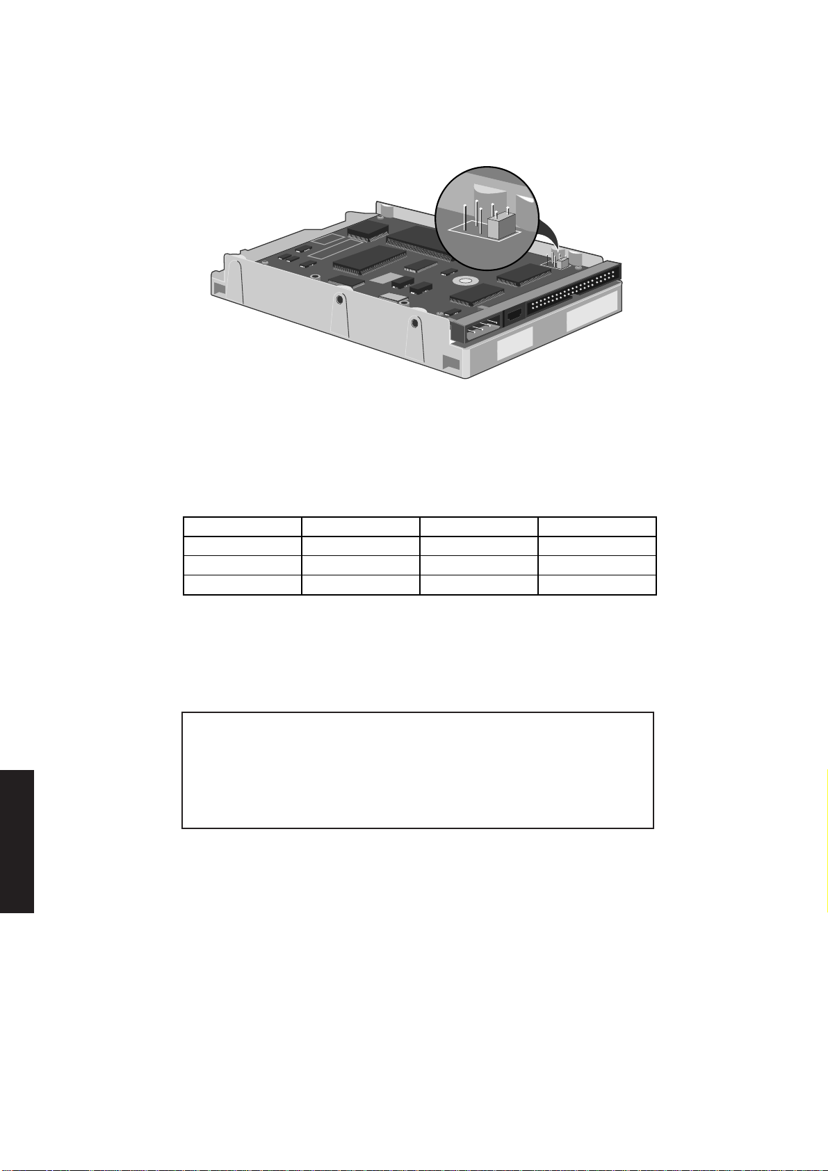
Preface
Peripheral items
Jumpers Three jumpers on the drive circuit are used to configure the drive. These are shown,
properly configured, in the following illustration.
The three jumpers are labelled DS (Drive select), CS (Cable select) and SP (Slave
present). The DS jumper must be fitted and the CS and SP jumpers not, in order for
the drive to function in an LS Pro.
Appendix C
Chapter 4
Chapter 4
Chapter 4
Drive formats The following table shows the physical format of the drives:
Drive 85 127 170
Disks 1 2 2
Heads 2 3 4
Tracks 3056 4584 6112
Formatting
These drives are low level formatted during manufacture. This format has been
optimized to allow the drive to provide maximum performance. Standard low level
formatting programs can only reduce the performance of the drive.
Warning
Do not attempt to perform a low level format on a ProDrive, this can only adversely affect
the performance of your drive. If you do try to format your drive most standard low level
formatting programs will return a “Drive formatted” message very quickly. In fact, the
drive has not been formatted.
Discache The Quantum ProDrive ELS drives are fitted with 32kbytes of RAM and look-ahead
cache circuitry known as Discache.
When a read access is made to the drive, Discache loads subsequent data into the RAM.
If an attempt is made to read this data it is accessed from RAM rather than from the
disk, thus considerably reducing access times.
Chapter 6 Appendix A
4/10 LS PRO HARDWARE TECHNICAL REFERENCE
Cache performance benefits tend to be application dependent. Discache has a number
of alterable parameters which allow the cache to be configured for maximum
performance benefit in any given application.
Full information on configuring Discache is given in the Quantum specification.

Maxtor 7213A
Jumpers Nine jumpers on the drive circuit are used to configure the drive. These are shown,
Peripheral items
Preface
The 213 Mbyte hard disk drive that may be fitted in the LS Pro range is a Maxtor 7213A.
It has a nominal access time of 15mS and can transfer data at up to 8.0 Mbytes per
second.
The drive circuit board contains the drive control electronics and a hard disk
controller. A read preamplifier and the write drive circuitry are located underneath
the drive cover.
The drive features an on-board media defect and error recovery scheme which is fully
user transparent.
Appendix A
properly configured, in the following illustration.
The jumpers are labelled J16 to J20 and J22 to J25. In the LS Pro application only J20
should be fitted. If J20 is not fitted or if any of the other jumpers are fitted the drive
is unlikely to operate correctly.
Drive format The drive has two disks and four data surfaces, and features a Universal Translate Mode
which allows it to be configured with any combination of cylinders, heads and sectors
within the drive’s formatted capacity.
Formatting
These drives are low level formatted during manufacture. This format has been
optimized to allow the drive to provide maximum performance. Standard low level
formatting programs can only reduce the performance of the drive.
Warning
Appendix C
Chapter 4
Chapter 4
Chapter 4
Chapter 6
Do not attempt to perform a low level format, this can only adversely affect the
performance of your drive. If you do try to format your drive most standard low level
formatting programs will return a “Drive formatted” message very quickly. In fact, the
drive has not been formatted.
LS PRO HARDWARE TECHNICAL REFERENCE 4/11

Preface
Peripheral items
Cache The drive is fitted with 64kbytes of RAM and read-ahead cache circuitry.
When a read access is made to the drive, subsequent data is read into the RAM. If an
attempt is made to read this data it is accessed from RAM rather than from the disk,
thus considerably reducing access times.
Quantum ProDrive LPS 240AT
The 240 Mbyte hard disk drive that may be fitted in the LS Pro range is a Quantum
ProDrive LPS 240AT. It has a nominal access time of 16mS and can transfer data at up
to 5.0 Mbytes per second.
The drive circuit board contains the drive control electronics and a hard disk
controller. A preamplifier for the read/write circuitry and an optical encoder are
located underneath the drive cover.
The drives feature an on-board media defect and error recovery scheme which is fully
user transparent.
Jumpers Four jumpers on the drive circuit are used to configure the drive. These are shown,
properly configured, in the following illustration.
Appendix C
Chapter 4
Chapter 4
Chapter 4
The jumpers are labelled CS (Cable select), DS (Drive select), SP (Slave present) and
DM (Drive Mode). The DS jumper must be fitted and the CS, SP and DM jumpers not,
in order for the drive to function in an LS Pro.
Drive format The physical format of the drive is as follows:
Disks 2
Heads 4
Tracks 7,200
Formatting
These drives are low level formatted during manufacture. This format has been
optimized to allow the drive to provide maximum performance. Standard low level
formatting programs can only reduce the performance of the drive.
Chapter 6 Appendix A
4/12 LS PRO HARDWARE TECHNICAL REFERENCE

Peripheral items
Warning
Do not attempt to perform a low level format on a ProDrive, this can only adversely affect
the performance of your drive. If you do try to format your drive most standard low level
formatting programs will return a “Drive formatted” message very quickly. In fact, the drive
has not been formatted.
Discache The ProDrive LPS 240AT drive is fitted with 256kbytes of RAM and look-ahead cache
circuitry known as Discache.
When a read access is made to the drive, Discache loads subsequent data into the RAM.
If an attempt is made to read this data it is accessed from RAM rather than from the
disk, thus considerably reducing access times.
Cache performance benefits tend to be application dependent. Discache has a number
of alterable parameters which allow the cache to be configured for maximum
performance benefit in any given application.
Full information on configuring Discache is given in the Quantum specification.
Preface
Appendix A
Quantum LPS525A
The 525 Mbyte hard disk drive that may be fitted in the LS Pro range is a Quantum
LPS525A. It has a nominal access time of 10mS and can transfer data at up to 5 Mbytes
per second.
The drive circuit board contains the drive control electronics and a hard disk
controller. The drive features an on-board media defect and error recovery scheme
which is fully user transparent.
Jumpers Three jumpers on the drive circuit are used to configure the drive. These are shown
in the following illustration.
Appendix C
Chapter 4
Chapter 4
Chapter 4
LS PRO HARDWARE TECHNICAL REFERENCE 4/13
Chapter 6

Preface
Peripheral items
The three jumpers are labelled DS (Drive select), CS (Cable select) and SP (Slave
present). In the LS Pro application the DS jumper must be fitted and the CS and SS
jumpers not.
Warning
None of the other jumpers are used in this application. If any of the other jumpers are installed
the drive will not function correctly.
Drive format The physical format of the drive is as follows:
Disks 3
Heads 6
Tracks 14,688
Formatting
The drive is low level formatted during manufacture. This format has been optimized
to allow the drive to provide maximum performance. Standard low level formatting
programs can only reduce the performance of the drive.
Appendix C
Chapter 4
Warning
Do not attempt to perform a low level format on a ProDrive, this can only adversely affect
the performance of your drive. If you do try to format your drive most standard low level
formatting programs will return a “Drive formatted” message very quickly. In fact, the drive
has not been formatted.
Discache The ProDrive LPS 525AT drive is fitted with 512kbytes of RAM and look-ahead cache
circuitry known as Discache.
When a read access is made to the drive, Discache loads subsequent data into the RAM.
If an attempt is made to read this data it is accessed from RAM rather than from the
disk, thus considerably reducing access times.
Cache performance benefits tend to be application dependent. Discache has a number
of alterable parameters which allow the cache to be configured for maximum
performance benefit in any given application.
Full information on configuring Discache is given in the Quantum specification.
Chapter 4
Chapter 4
Chapter 6 Appendix A
4/14 LS PRO HARDWARE TECHNICAL REFERENCE

IDE interface
Interface signal Host reset
descriptions
Reset signal from the system board. Active low during system power up.
Host data 0-15
16-bit bidirectional data bus between the system board and the drive.
Host I/O channel ready
These two lines allow the drive to lengthen I/O read and write cycles by generating
system board wait states. These lines are normally high and are driven low by the drive
if an I/O cycle is to be lengthened.
Host IOW
Write strobe. This signal clocks data from the system board to the drive on the data
bus.
Host IOR
Read strobe. This signal clocks data from the drive to the system board on the data bus.
Peripheral items
Preface
Appendix A
Appendix C
Host ALE
System board Address Latch Enable. This signal is not used by the drive, it is provided
for compatibility.
Host IRQ14
This is the interrupt signal to the system board. This signal is active high when the drive
is selected and the drive interrupt enable bit (IEN) is activated by the system board. An
interrupt is cleared upon receiving the next command, when the status register is read,
or when the drive is reset.
Host IOCS16
Informs the system board that the drive data register has been enabled and the drive
is prepared to perform a 16-bit I/O transfer.
Host ADDR 0-2
These lines are used to select registers on the drive.
Chapter 4
Chapter 4
Chapter 4
Chapter 6
LS PRO HARDWARE TECHNICAL REFERENCE 4/15

Peripheral items
Connectors Control Connector
Preface
Pin Function Pin Function
1 host reset- 21 host I/O channel ready2 ground 22 ground
3 host data 7 23 host IOW4 host data 8 24 ground
5 host data 6 25 host IOR-
6 host data 9 26 ground
7 host data 5 27 host I/O channel ready8 host data 10 28 host ALE
9 host data 4 29 reserved
10 host data 11 30 ground
11 host data 3 31 host IRQ14
12 host data 12 32 host IOCS16-
13 host data 2 33 host ADDR1
14 host data 13 34 15 host data 1 35 host ADDR0
16 host data 14 36 host ADDR2
17 host data 0 37 18 host data 15 38 -
19 ground 39 20 key 40 ground
Appendix C
Chapter 4
Chapter 4
Chapter 4
The pin layout of the connector.
Power connector
Pin Function
1 +12 Volts
2 ground (for +12V)
3 ground (for +5V)
4 +5 Volts
2
1
4
2
3
40
39
1
Chapter 6 Appendix A
4/16 LS PRO HARDWARE TECHNICAL REFERENCE

4.4 FLOPPY DRIVE
DRIVE SELECT
SWITCH
Description
The floppy disk drive fitted in the LS Pro range is a 3.5", high density double-sided, one
inch high unit. The drive can read and write 3.5" discs with a formatted capacity of either
1.44Mbytes or 720 kbytes. The drive has a constant disk rotation speed of 300 rpm.
The different disk capacities are accommodated by different data transfer rates.
The 1.44 Mbyte media uses a data transfer rate of 500 kbits/sec. The 720 kbyte media
uses a data transfer rate of 250 kbits/sec.
Peripheral items
Preface
Both types of media are double-sided with 80 tracks per side and a track density of 135
tracks per inch.
Drive select The drive select switch is set to identify the drive to the system. The switch is located
switch at the rear of the drive on the right-hand side. The switch is set to 0. The drive select
switch is shown below.
Disk format 1.44 Mbyte disks have a hole in the disk in the opposite corner to the write protect tab.
The drive uses this to determine the type of disk fitted. If the drive does not detect a
hole in the disk it treats it as a 720kbyte disk and changes the transfer rate to 250 kbits
per second.
Appendix A
Appendix C
Chapter 4
The following details briefly describe the floppy disk formats for the two capacities of
disk.
720 kbytes disks
• double-sided
• 80 tracks/side
• 512 bytes/sector
• 9 sectors/track
1.44 Mbyte disks
• double-sided
• 80 tracks/side
• 512 bytes/sector
• 18 sectors/track
LS PRO HARDWARE TECHNICAL REFERENCE 4/17
Chapter 4
Chapter 4
Chapter 6

Peripheral items
Interface
Preface
The drive has one connector. The pinout of the connector and an illustration are shown
below.
Connector
Signal Density select 0,1
descriptions
Pin Function Pin Function
Note
All other pins are connected to 0 Volts.
Not currently used.
2 density select 1 14 drive select 2
3 not connected 16 motor on
4 not connected 18 direction
5 5V 20 step
6 density select 0 22 write data
7 5V 24 write enable
8 index 26 track 00
9 5V 28 write protect
10 drive select 0 30 read data
11 5V 32 head select
12 drive select 1 34 disk change
2
1
34
33
Appendix C
Chapter 4
Chapter 4
Chapter 4
Chapter 6 Appendix A
Drive select 0,1,2
The drive select inputs are used to enable and disable the other input/output lines.
When a select input is low the drive is active and the input/output lines are enabled.
When a select input is high, all outputs from the drive are disabled and all inputs are
ignored.
Index
When the drive is selected this line is pulsed low for each revolution of the disk drive
spindle.
Motor on
When this input is taken low and a disk is inserted in the drive, the drive motor starts.
When this input is taken high or a disk is removed the drive motor stops.
Direction
If this input is high the step input causes the read/write head to step away from the
centre of the disk. If this input is low the head steps toward the centre of the disk.
Step
A low pulse on this input will cause the read/write head to move to the next track. The
direction of movement is determined by the direction input at the end of the step pulse.
4/18 LS PRO HARDWARE TECHNICAL REFERENCE

Peripheral items
Write data
If the write gate input is low, a low pulse on this input will write a bit of data on the disk.
Write gate
If this input is low, the write circuitry is enabled and data can be written to the disk via
the write data input.
Track 00
This is an output which is low when the read/write head is positioned on track 00 of
the disk.
Preface
Write protect
If a write protected disk is in the drive this output is low and the drive is unable to write
data.
Read data
When the drive is selected a low pulse is generated for each bit on the disk that is
detected.
Head select
This input selects the read/write head. If low, head 1 is selected, if high, head 0 is
selected.
Disk change
This output is low whenever a disk is removed from the drive. It remains low until a
disk is inserted, and the disk change reset signal has been received.
4.5 KEYBOARD
Appendix A
Appendix C
Chapter 4
Introduction
The keyboard has 102-keys in the same layout as the IBM AT enhanced keyboard. It
provides the full range of QWERTY typewriter keys, special editing and function keys
and a number pad at the right hand side of the keyboard.
The following illustration shows the layout of the keys and the key legends on the UK
keyboard.
apricot
F2 F3
F1
Esc
£3$
!
1 2
4
Q
W
A S D F G
Caps Lock
|
X
Z
\
Ctrl
Alt
F4
F6
F7
F5
&
%
^
*
8
5
6 7
YT
RE
H J
NBV
C
M
K
F8
(
9 0
<
,
L
)
POIU
:
;
>
.
F10 F12
F9
_
+
- =
{
[
@
'
?
/
Alt Gr
LS PRO HARDWARE TECHNICAL REFERENCE 4/19
Print
Pause
Scroll
Scrn
F11
}
]
~
#
Lock
SysRq
Break
1
A
Num
Page
Home
Insert
Up
Page
Delete
End
Down
Ctri
/
Lock
8
7
Home
5
4
1 2 3
End
0
Ins
*
9
Pg Up
6
Pg Dn
.
Del
-
+
Enter
Chapter 4
Chapter 4
Chapter 6

Peripheral items
Operation
Preface
Commands to The keyboard sends data and command codes to the system unit. The commands that
the system unit the keyboard can send are described in the following table.
Appendix C
The keyboard communicates with the keyboard interface in the system unit using two
lines: clock and data. These lines are driven by both the keyboard and the system unit.
The keyboard provides the clock for both transmitting and receiving.
Communication is bi-directional. The system unit can send commands to the keyboard
as well as the keyboard sending scan codes to the system unit. The keyboard first checks
the clock line: if it is low, pending scan codes are loaded into the keyboard buffer; if the
clock line is high the keyboard checks the data line.
If the data line is low the keyboard receives commands from the system unit, if the data
line is high the keyboard sends data to the system unit. The data consists of: one start
bit; eight data bits; and one parity bit. Each time the keyboard takes the clock line high
it checks to see if the system unit is pulling the line low. If the line has been pulled low
the code being transmitted is saved and the keyboard enters the receive mode.
Command Function
FEh resend
FCh self-test failure
FAh acknowledge
EEh echo response
AAh self-test pass
00h or FFh buffer overflow
83ABh identification byte
Chapter 4
Chapter 4
Chapter 4
Chapter 6 Appendix A
Resend (FEh)
The keyboard sends this command to the system unit if it receives an invalid command,
or a command with bad parity.
Self-test failure (FCh)
If the keyboard RAM or ROM self-test fails, this command is sent.
Acknowledge (FAh)
The keyboard sends this command after receiving a valid input from the system unit.
There are two exceptions: in response to an echo command; and usually in response
to a resend command. However, a resend command will result in an acknowledge
response if acknowledge was the last transmission to the keyboard.
Echo (EEh)
This is sent in response to an echo command from the system unit.
Self-test pass (AAh)
This code is sent to the system unit if the keyboard RAM and ROM self-test is passed.
4/20 LS PRO HARDWARE TECHNICAL REFERENCE

Peripheral items
Buffer overflow (00h or FFh)
This code is sent to the system unit when the type ahead buffer overflows. 00h is sent
if code sets 2 or 3 are in use; FFh is sent if code set 1 is in use.
Identification byte (83ABh)
These bytes are sent to the system unit in response to a read ID command. The
keyboard stops scanning, sends the ID bytes, then continues scanning. The least
significant byte is sent first.
Commands from Commands are sent from the system unit to the keyboard via the keyboard controller
the system unit data buffer. The controller inserts a parity bit and transmits the data serially to the
keyboard. No further transmission is sent to the keyboard until the keyboard
acknowledges receipt of the data byte.
The command bytes which the keyboard recognises are listed below.
Command Description
EDh Set/reset LED indicators
EEh Echo
EFh No operation
F0h Select alternate scan codes
F1h No operation
F2h Read ID
F3h Set typematic rate/delay
F4h Enable
F5h Default disable
F6h Set default
F7h Set all keys typematic
F8h Set all keys make/break
F9h Set all keys make only
FAh Set all keys typematic/make/break
FBh Set key to typematic
FCh Set key to make/break
FEh Resend
FFh Reset
Preface
Appendix A
Appendix C
Chapter 4
Chapter 4
Chapter 4
When the keyboard receives any of these commands, it sends an ACKnowledge (FAh)
response. If the data is incorrectly received the keyboard sends a RESEND (FEh)
request.
The use and formats of these commands is described in the following paragraphs.
LS PRO HARDWARE TECHNICAL REFERENCE 4/21
Chapter 6

Preface
Peripheral items
Set/reset LED indicators (EDh)
This command is used to set the LEDs on the keyboard. When the keyboard receives
this command it responds with the ACK (FAh). The controller then sends the
parameter byte. On receipt of the parameter byte the keyboard updates the LEDs. The
format of the parameter byte is shown below:
7 6 5 4 3 2 1 0
scroll lock LED
num lock LED
caps lock LED
reserved
Note
Bit 7 must be set to 0.
Echo (EEh)
The keyboard responds to this command by sending an “echo response” (EEh), and
then continues with normal operation.
Appendix C
Chapter 4
Chapter 4
Chapter 4
Set typematic rate/delay (F3h)
The keyboard responds with an ACK, stops scanning, and waits for the rate/delay byte
from the system unit. The format of the byte is as follows.
7 6 5 4 3 2 1 0
rate
delay
reserved (always 0)
Rate Parameter
The typematic rate (number of make codes per second) is from 2 make codes per
second with bits D0 to D4 all set to 1, to 30 make codes per second, with bits D0 to
D4 all set to 0.
Delay Parameter
The delay before the typematic operation comes into effect is shown in the table below:
D6 D5 Delay
0 0 250mS
0 1 500mS
1 0 750mS
1 1 1000mS
Chapter 6 Appendix A
4/22 LS PRO HARDWARE TECHNICAL REFERENCE
Enable (F4h)
The keyboard responds with an ACK, clears its output buffer, and enables key scanning
and keycode transmission.

Peripheral items
Default disable (F5h)
The keyboard performs the same functions as “Set default” except that further
scanning and transmission is disabled.
Set default (F6h)
The keyboard resets, clears its buffers, and responds with an ACK. If it was previously
enabled it then resumes normal scanning/transmission.
Set all keys (F7h, F8h, F9h and FAh)
These commands are only valid when the keyboard is set to “code set three”. The
different code sets are described elsewhere in this section. The commands set all of
the keys to be the type specified: typematic (F7h), make/break (F8h), make only (F9h)
and typematic/make/break (FAh).
Set key type (FBh, FCh and FDh)
These commands are only valid when the keyboard is set to “code set three”. The
different code sets are described elsewhere in this section. The commands set
individual keys to be the type specified: typematic (FBh), make/break (FCh) and make
only (FDh). The command is first sent, the keyboard acknowledges the command and
waits for the key scan code to be sent. One or more key codes can be sent. The
keyboard then waits for an ENABLE (F4h) before resuming scanning.
Preface
Appendix A
Appendix C
Scan codes
Resend (FEh)
The keyboard resends the last code sent to the system unit.
Reset (FFh)
The keyboard responds with an ACK, performs a set of internal diagnostics, clears its
key buffer, and then sets the typematic rate/delay to the default values.
Three sets of scan codes are available. The keyboard normally selects code set 2 (AT
compatible). The other sets may be selected using select alternative scan codes
command (F0h).
The following diagram numbers the positions which are referred to in the following
scan code tables.
110
1 2 3
16
44
45
58
112 113
17
464748
115
5
6 7
34
49 50
116 117
8910
35
51
61
114
4
18
192021 222324 25 26 27
33323130
118
38
3736
525354
119
120 121
12 13
11
4039
55
6260
123
122
15
28
43
42
41
57
64
126
124
125
95
85
75
76
79
90
80
91
86
81
92 97 102
83
93
89
84
105
100
96
101
106
98
103
99
108
104
Chapter 4
Chapter 4
Chapter 4
Chapter 6
LS PRO HARDWARE TECHNICAL REFERENCE 4/23

Preface
Peripheral items
Scan code set 1 These scan codes are compatible with the PC/XT keyboard scan codes. Each key is
assigned a make code which is sent to the keyboard buffer when the key is pressed. The
break code is sent when the key is released. The break codes are generated by adding
80h to the make codes. Notice that some of the scan codes have additional codes.
These are for additional keys and to indicate shift states.
The codes are listed in the following table:
Scan code set 1
Appendix C
Chapter 4
Chapter 4
Chapter 4
Chapter 6 Appendix A
Key
Number
1 29 A9 44 2A AA
2 02 82 45 56 D6
3 03 83 46 2C AC
4 04 84 47 2D AD
5 05 85 48 2E AE
6 06 86 49 2F AF
7 07 87 50 30 B0
8 08 88 51 31 B1
9 09 89 52 32 B2
10 0A 8A 53 33 B3
11 0B 8B 54 34 B4
12 0C 8C 55 35 B5
13 0D 8D 57 36 B6
15 0E 8E 58 1D 9D
16 0F 8F 60 38 B8
17 10 90 61 39 B9
18 11 91 62 E0 38 E0 B8
19 12 92 64 E0 1D E0 9D
20 13 93 90 45 C5
21 14 94 91 47 C7
22 15 95 92 4B CB
23 16 96 93 4F CF
24 17 97 95 E0 35 E0 B5
25 18 98 96 48 C8
26 19 99 97 4C CC
27 1A 9A 98 50 D0
28 1B 9B 99 52 D2
30 3A BA 100 37 B7
31 1E 9E 101 49 C9
32 1F 9F 102 4D CD
33 20 A0 103 51 D1
34 21 A1 104 53 D3
35 22 A2 105 4A CA
36 23 A3 106 4E CE
37 24 A4 108 E0 1C E0 9C
38 25 A5 110 01 81
39 26 A6 112 3B BB
40 27 A7 113 3C BC
41 28 A8 114 3D BD
42 2B AB 115 3E BE
43 1C 9C 116 3F BF
Make
Code
Break
Code
Key
Number
Make
Code
Break
Code
4/24 LS PRO HARDWARE TECHNICAL REFERENCE

Peripheral items
Preface
Key
Number
117 40 C0 Num Lock key active
118 41 C1 75 E0 2A E0 52 E0 D2 E0 AA
119 42 C2 76 E0 2A E0 53 E0 D3 E0 AA
120 43 C3 79 E0 2A E0 4B E0 CB E0 AA
121 44 C4 80 E0 2A E0 47 E0 C7 E0 AA
122 57 D7 81 E0 2A E0 4F E0 CF E0 AA
123 58 D8 83 E0 2A E0 48 E0 C8 E0 AA
124 E0 2A E0 B7 84 E0 2A E0 50 E0 D0 E0 AA
125 46 C6 86 E0 2A E0 51 E0 D1 E0 AA
126 E1 D1 45 This key 89 E0 2A E0 4D E0 CD E0 AA
Lower-case or Shift and Num Lock keys active 124 54 D4
75 E0 52 E0 D2 Ctrl key active
76 E0 53 E0 D3 126 E0 46 E0 C6 This key
79 E0 4B E0 CB does not
80 E0 47 E0 C7 have a
81 E0 4F E0 CF break code
83 E0 48 E0 C8
84 E0 50 E0 D0
85 E0 49 E0 C9
86 E0 51 E0 D1
89 E0 4D E0 CD
Shift key active
75 E0 AA E0 52 E0 D2 E0 2A
76 E0 AA E0 53 E0 D3 E0 2A
79 E0 AA E0 4B E0 CB E0 2A
80 E0 AA E0 47 E0 C7 E0 2A
81 E0 AA E0 4F E0 CF E0 2A
83 E0 AA E0 48 E0 C8 E0 2A
84 E0 AA E0 50 E0 D0 D0 2A
85 E0 AA E0 49 E0 C9 E0 2A
86 E0 AA E0 51 E0 D1 E0 2A
89 E0 AA E0 4D E0 CD E0 2A
95 E0 AA E0 35 E0 B5 E0 2A
Make
Code
E0 37 E0 AA 85 E0 2A E0 49 E0 C9 E0 AA
E1 9D C5 does not Ctrl or Shift keys active
Break
Code
have a 124 E0 37 E0 B7
break code Alt key active
Key
Number
Make
Code
Break
Code
Appendix A
Appendix C
Chapter 4
Chapter 4
Chapter 4
LS PRO HARDWARE TECHNICAL REFERENCE 4/25
Chapter 6

Preface
Peripheral items
Scan code set 2 These scan codes are AT/PS/2 compatible. Each key is assigned a make code which is
sent to the keyboard buffer when the key is pressed. The break code is sent when the
key is released. The break codes are produced by sending F0h followed by the make
code. Notice that some of the scan codes have additional codes to indicate the various
shift states.
Scan Code set 2
Appendix C
Chapter 4
Chapter 4
Chapter 4
Chapter 6 Appendix A
Key
Number
1 0E F0 0E 43 5A F0 5A
2 16 F0 16 44 12 F0 12
3 1E F0 1E 45 61 F0 61
4 26 F0 26 46 1A F0 1A
5 25 F0 25 47 22 F0 22
6 2E F0 2E 48 21 F0 21
7 36 F0 36 49 2A F0 2A
8 3D F0 3D 50 32 F0 32
9 3E F0 3E 51 31 F0 32
10 46 F0 46 52 3A F0 3A
11 45 F0 45 53 41 F0 41
12 4E F0 4E 54 49 F0 49
13 55 F0 55 55 4A F0 4A
15 66 F0 66 57 59 F0 59
16 0D F0 0D 58 14 F0 14
17 15 F0 15 60 11 F0 11
18 1D F0 1D 61 29 F0 29
19 24 F0 24 62 E0 11 E0 F0 11
20 2D F0 2D 64 E0 14 E0 F0 14
21 2C F0 2C 90 77 F0 77
22 35 F0 35 91 6C F0 6C
23 3C F0 3C 92 68 F0 68
24 43 F0 43 93 69 F0 69
25 44 F0 44 95 E0 4A E0 F0 4A
26 4D F0 4D 96 75 F0 75
27 54 F0 54 97 73 F0 73
28 5B F0 5B 98 72 F0 72
30 58 F0 58 99 70 F0 70
31 1C F0 1C 100 7C F0 7C
32 1B F0 1B 101 7D F0 7D
33 23 F0 23 102 74 F0 74
34 2B F0 2B 103 7A F0 7A
35 34 F0 34 104 71 F0 71
36 33 F0 33 105 7B F0 7B
37 3B F0 3B 106 79 F0 79
38 42 F0 42 108 E0 5A E0 F0 5A
39 4B F0 4B 110 76 F0 76
40 4C F0 4C 112 05 F0 05
41 52 F0 52 113 06 F0 06
42 5D F0 5D 114 04 F0 04
Make
Code
Break
Code
Key
Number
Make
Code
Break
Code
4/26 LS PRO HARDWARE TECHNICAL REFERENCE

Peripheral items
Preface
Key
Number
115 0C F0 0C Shift key active
116 03 F0 03 75 E0 F0 12 E0 70 E0 F0 70 E0 12
117 0B F0 0B 76 E0 F0 12 E0 71 E0 F0 71 E0 12
118 83 F0 83 79 E0 F0 12 E0 6B E0 F0 6B E0 12
119 0A F0 0A 80 E0 F0 12 E0 6C E0 F0 6C E0 12
120 01 F0 01 81 E0 F0 12 E0 69 E0 F0 69 E0 12
121 09 F0 09 83 E0 F0 12 E0 75 E0 F0 75 E0 12
122 78 F0 78 84 E0 F0 12 E0 7D E0 F0 7D E0 12
123 07 F0 07 85 E0 F0 12 E0 7A E0 F0 7A E0 12
124 E0 12 E0 E0 F0 7C 86 E0 F0 12 E0 74 E0 F0 74 E0 12
125 7E F0 7E 95 E0 F0 12 4A E0 12 F0 4A
126 E1 14 77 E1 This key Num Lock key active
Lower-case or Shift and Num Lock keys active 80 E0 12 E0 6C
75 E0 70 E0 F0 70 81 E0 12 E0 69
76 E0 71 E0 F0 71 83 E0 12 E0 75
79 E0 6B E0 F0 6B 84 E0 12 E0 72
80 E0 6C E0 F0 6C 85 E0 12 E0 7D
81 E0 69 E0 F0 69 86 E0 12 E0 7A
83 E0 75 E0 F0 75 89 E0 12 E0 74
84 E0 72 E0 F0 72 Ctrl or Shift keys active
85 E0 7D E0 F0 7D 124 E0 7C E0 F0 7C
86 E0 7A E0 F0 7A Alt key active
89 E0 74 E0 F0 74 124 84 F0 84
Make
Code
7C E0 F0 12 89 E0 F0 12 E0 74 E0 F0 74 E0 12
F0 14 F0 77 does not 75 E0 12 E0 70
Break
Code
have a 76 E0 12 E0 71
break code 79 E0 12 E0 6B
Key
Number
Ctrl key active
126 E0 7E E0 This key does
Make
Code
F0 7E not have a
E0 F0 70 E0 F0 12
E0 F0 71 E0 F0 12
E0 F0 6B E0 F0 12
E0 F0 6C E0 F0 12
E0 F0 69 E0 F0 12
E0 F0 75 E0 F0 12
E0 F0 72 E0 F0 12
E0 F0 7D E0 F0 12
E0 F0 7A E0 F0 12
E0 F0 74 E0 F0 12
break code
Break
Code
Appendix A
Appendix C
Chapter 4
Chapter 4
Chapter 4
LS PRO HARDWARE TECHNICAL REFERENCE 4/27
Chapter 6

Preface
Peripheral items
Scan set 3 Each key is assigned a make code which is sent to the keyboard buffer when the key
is pressed. The break code is sent when the key is released. The break codes are
produced by sending F0h followed by the make code. The codes are not affected by
any shift states within the keyboard. The keys are defined as typematic, make/break or
make only. The type of key can be changed by using the set all keys command (F7, F8,
F9, FA) to the keyboard from the system unit.
Scan Code set 3
Appendix C
Chapter 4
Chapter 4
Chapter 4
Chapter 6 Appendix A
Key
Number
1 0E F0 0E Typematic 41 52 F0 52 Typematic
2 16 F0 16 Typematic 42 53 F0 53 Typematic
3 1E F0 1E Typematic 43 5A F0 5A Typematic
4 26 F0 26 Typematic 44 12 F0 12
5 25 F0 25 Typematic 45 13 F0 13 Typematic
6 2E F0 2E Typematic 46 1A F0 1A Typematic
7 36 F0 36 Typematic 47 22 F0 22 Typematic
8 3D F0 3D Typematic 48 21 F0 21 Typematic
9 3E F0 3E Typematic 49 2A F0 2A Typematic
10 46 F0 46 Typematic 50 32 F0 32 Typematic
11 45 F0 45 Typematic 51 31 F0 31 Typematic
12 4E F0 4E Typematic 52 3A F0 3A Typematic
13 55 F0 55 Typematic 53 41 F0 41 Typematic
15 66 F0 66 Typematic 54 49 F0 49 Typematic
16 0D F0 0D Typematic 55 4A F0 4A Typematic
17 15 F0 15 Typematic 57 59 F0 59
18 1D F0 1D Typematic 58 11 F0 11
19 24 F0 24 Typematic 60 19 F0 19
20 2D F0 2D Typematic 61 29 F0 29 Typematic
21 2C F0 2C Typematic 62 39 F0 39 Make only
22 35 F0 35 Typematic 64 58 F0 58 Make only
23 3C F0 3C Typematic 75 67 F0 67 Make only
24 43 F0 43 Typematic 76 64 F0 64 Typematic
25 44 F0 44 Typematic 79 61 F0 61 Typematic
26 4D F0 4D Typematic 80 6E F0 6E Make only
27 54 F0 54 Typematic 81 65 FO 65 Make only
28 5B F0 5B Typematic 83 63 F0 63 Typematic
30 14 F0 14
31 1C F0 1C Typematic 85 6F F0 6F Make only
32 1B F0 1B Typematic 86 6D F0 6D Make only
33 23 F0 23 Typematic 89 6A F0 6A Typematic
34 2B F0 2B Typematic 90 76 F0 76 Make only
35 34 F0 34 Typematic 91 6C F0 6C Make only
36 33 F0 33 Typematic 92 6B F0 6B Make only
37 3B F0 3B Typematic 93 69 F0 69 Make only
38 42 F0 42 Typematic 95 77 F0 77 Make only
39 4B F0 4B Typematic 96 75 F0 75 Make only
40 4C F0 4C Typematic 97 73 F0 73 Make only
Make
Code
Break
Code
Key
type
Make/break
Key
Number
84 60 F0 60 Typematic
Make
Code
Break
Code
Make/break
Make/break
Make/break
Make/break
Key
type
4/28 LS PRO HARDWARE TECHNICAL REFERENCE

Peripheral items
Preface
Connector
Key
Number
98 72 F0 72 Make only 115 1F F0 1F Make only
100 7E F0 7E Make only 116 27 F0 27 Make only
101 7D F0 7D Make only 117 2F F0 2F Make only
102 74 F0 74 Make only 118 37 F0 37 Make only
103 7A F0 7A Make only 119 3F F0 3F Make only
104 71 F0 71 Make only 120 47 F0 47 Make only
105 84 F0 84 Make only 121 4F F0 4F Make only
106 7C F0 7C Typematic 122 56 F0 56 Make only
108 79 F0 79 Make only 123 5E F0 5E Make only
110 08 F0 08 Make only 124 57 F0 57 Make only
112 07 F0 07 Make only 125 5F F0 5F Make only
113 0F F0 0F Make only 126 62 F0 62 Make only
114 17 F0 17 Make only
Make
Code
Break
Code
Key
type
Key
Number
Make
Code
Break
Code
Key
type
The keyboard is connected to the system unit via a 6-pin miniature DIN connector. The
pinout and connector details are given below.
Appendix A
Appendix C
Pin I/O Signal name
1 I/O Data
2 NA Reserved
3 NA Ground
4 NA +5Vdc
5 I/O Clock
6 NA Reserved
5
6
3
4
2
1
Chapter 4
Chapter 4
Chapter 4
Chapter 6
LS PRO HARDWARE TECHNICAL REFERENCE 4/29

Peripheral items
4.6 KeyLOC CARD
Preface
The KeyLOC card is a credit card sized unit which is used in conjunction with the
Apricot LOC Technology software to control access to the computer and the data
stored on it.
The KeyLOC card consists of a plastic case and a small circuit board. The plastic case
is in two halves and contains the circuit board and three small batteries. The case may
be opened in order to replace the batteries, this is done by sliding the two halves apart.
The batteries should be replaced with Duracell 389 or equivalent and should be placed
in the holder positive pole upwards.
Note
Take care not to touch the surfaces of the batteries during installation.
BATTERIES
Appendix C
Chapter 4
Chapter 4
Chapter 4
The circuit board contains a small 4-bit microprocessor system, a switch and an infra
red transmitter. Each time the switch is operated the microprocessor generates a
pseudo-random bit pattern which is transmitted by the infra red transmitter. This signal
is received by the infra red detector on the LED card within the system unit and passed
to the security sub-system on the system board.
Chapter 6 Appendix A
4/30 LS PRO HARDWARE TECHNICAL REFERENCE

MEMORY AND I/O USAGE
Chapter 5

Contents
Memory and I/O Usage
Preface
5 MEMORY AND I/O USAGE
5.1 Introduction ............................. 5/2
5.2 Memory usage ........................ 5/2
Shadowing disabled................ 5/3
Shadowing enabled ................ 5/3
5.3 I/O space .................................. 5/4
DMA I/O address map ............ 5/5
Interrupt controllers................. 5/6
System timers ............................ 5/6
Keyboard controller ................ 5/6
Command/status port.......... 5/6
Port B .......................................... 5/8
Write operations.................. 5/8
Read operations.................... 5/8
RTC RAM/NMI mask............... 5/9
SCAMP registers...................... 5/10
EMS index register and data
ports ....................................... 5/10
Configuration index and data
registers ................................. 5/10
Apricot ports............................ 5/11
LAN LED ............................... 5/11
1.6 Mbyte floppy .................. 5/12
IOCHCK................................ 5/12
Option ROM page............... 5/12
Token-ring daughterboard 5/12
Microphone level control .. 5/13
Hard disk drive controller
registers .................................... 5/14
Serial port controller
registers .................................... 5/14
Ethernet controller ................. 5/15
82596 PORT address.......... 5/15
82596 CA address............... 5/15
Ethernet ID PROM.............. 5/15
Ethernet status register...... 5/15
Business audio .......................... 5/17
Address .................................. 5/17
Data ports ............................. 5/17
Floppy disk controller............ 5/17
Parallel port controller.......... 5/18
Data address port............... 5/18
Status Port............................ 5/18
Parallel control port........... 5/19
Video DAC .............................. 5/19
VGA Registers......................... 5/20
General registers ................ 5/21
Sequencer registers............ 5/21
CRT Controller registers . 5/22
Graphics controller
registers ................................ 5/23
Attribute controller
registers ................................ 5/23
CL-GD542X Extension
registers .................................... 5/25
Appendix A
Appendix C
Chapter 4
LS PRO HARDWARE TECHNICAL REFERENCE 5/1
Chapter 6
Chapter 4
Chapter 5

Memory and I/O Usage
5.1 INTRODUCTION
Preface
5.2 MEMORY USAGE
Appendix C
This section describes Memory and I/O space layout, and details the usage of the
registers in I/O space.
The memory map below details the addressing of system board memory.
16M
16M-128k
1M
960k
768k
640k
SYSTEM BOARD ROM
EXPANSION RAM
BIOS
BUS MEMORY
VIDEO RAM
FFFFFFh
FE0000h
100000h
0F0000h
0E0000h896k
0C0000h
0A0000h
Chapter 4
Chapter 6 Appendix A
Chapter 4
Chapter 5
SYSTEM BOARD RAM
0
000000h
Note
The SETUP utility allows BIOS shadowing to be enabled or disabled. If shadowing is enabled
the BIOS on the system board is copied into RAM where it can be accessed faster.
A more detailed description of the region between 768k and 1M (0C0000h and
100000h) is given over.
5/2 LS PRO HARDWARE TECHNICAL REFERENCE

Memory and I/O Usage
Preface
1M
976K
960K
928K
896K
SHADOWING
DISABLED
BIOS
82596 RPL and
SECURITY
GRAPHICAL BOOT
and SETUP
VIDEO BIOS
BUS
MEMORY
100000
F4000
F0000
E8000
E0000
1M
976K
960K
928K
912K
896K
SHADOWING
ENABLED
BIOS
82596 RPL and
SECURITY
GRAPHICAL BOOT
and SETUP
NOTE 1
BUS
MEMORY
100000
F4000
F0000
E8000
E4000
E0000
Appendix A
Appendix C
C8000
C0000
784K
768K
NOTE 1
C4000
C0000
800K
VIDEO BIOS
768K
Notes
1. This area is occupied by the ROM in the option ROM socket if it is fitted.
2. These memory maps do not include the Token-Ring module RAM and ROM. If fitted
the ROM occupies an 16k block between CC000h and D0000h. The RAM buffer size
and base address are configured by the adapter driver.
The video BIOS, graphical boot and SETUP, 82596 RPL and security and system BIOS
code are all in the main 128kbyte system ROM. After boot is completed only the video
BIOS and system BIOS code is required.
Shadowing With shadowing disabled and the option ROM socket empty the regions from C0000
disabled to E0000 and from E8000 to F4000 are available as UMB space for DOS.
Shadowing When shadowing is enabled the video BIOS is remapped to the C0000 to C8000 area.
enabled Thus with the shadowing enabled and the option ROM socket empty the region from
C8000 to F4000 is available as UMB space for DOS. This is the same amount of UMB
as is available with shadowing disabled, but it is contiguous. This often allows DOS to
make better use of the available space.
Chapter 4
Chapter 6
Chapter 4
Chapter 5
Note
The Rev C system board has a slightly different memory map, refer to Appendix B for details.
LS PRO HARDWARE TECHNICAL REFERENCE 5/3

Memory and I/O Usage
5.3 I/O SPACE
Preface
Appendix C
Chapter 4
The table below shows the general use of I/O space on the LS Pro system board. The
pages which follow describe in more detail specific ports and groups of ports.
Addresses (hex) Device
0000-000F Master DMA controller
0020-0021 Master interrupt controller
0040-0043 System timers
0060 Keyboard controller
0061 Port B (PPI control port)
0064 Keyboard controller
0070-0071 RTC RAM/NMI mask
0080-008F DMA page registers
00A0-00A1 Slave interrupt controller
00C0-00DF Slave DMA controller
00E8-00FE SCAMP
0120-012F Apricot ports
01F0-01F7 Hard disk drive
02F8-02FF Serial port 2
0300-030F Ethernet controller
0388-038F Business audio
03B4, 03B5, 03BA VGA
03BC-03BE Parallel port controller
03C0-03C5 VGA
03C6-03C9 Video DAC
03CE, 03CF, 03D4 VGA
03D5, 03DA VGA
03F2-03F5 Floppy disk controller
03F6, 03F7 Floppy and hard disk controller
03F8-03FF Serial port 1
46E8 VGA setup
Chapter 6 Appendix A
Chapter 4
Chapter 5
5/4 LS PRO HARDWARE TECHNICAL REFERENCE

DMA I/O address map
The following table shows the I/O addresses used by the DMA Controller and their
significance. Full information on the programming of 8237 DMA controller registers are
given in manufacturers data sheets and are not repeated here
Address (hex) Function
0000 Channel 0 Memory address register
0001 Channel 0 Transfer count register
0002 Channel 1 Memory address register
0003 Channel 1 Transfer count register
0004 Channel 2 Memory address register
0005 Channel 2 Transfer count register
0006 Channel 3 Memory address register
0007 Channel 3 Transfer count register
0008 Channel 0-3 Status register
0009 Reserved
000A Channel 0-3 Mask Register (set/reset)
000B Channel 0-3 Mode register (write)
000C Clear byte pointer (write)
000D Master clear (write)
000E Channel 0-3 Clear mask register (write)
000F Channel 0-3 Write mask register
Memory and I/O Usage
Preface
Appendix A
Appendix C
0080 Diagnostic checkpoint port
0081 Channel 2 Page table address register
0082 Channel 3 Page table address register
0083 Channel 1 Page table address register
0087 Channel 0 Page table address register
0089 Channel 6 Page table address register
008A Channel 7 Page table address register
008B Channel 5 Page table address register
008F Channel 4 Page table address register
00C0 Channel 4 Memory address register
00C2 Channel 4 Transfer count register
00C4 Channel 5 Memory address register
00C6 Channel 5 Transfer count register
00C8 Channel 6 Memory address register
00CA Channel 6 Transfer count register
00CC Channel 7 Memory address register
00CE Channel 7 Transfer count register
00D0 Channel 4-7 Status register
00D4 Channel 4-7 Mask register (set/reset)
00D6 Channel 4-7 Mode register (write)
00D8 Clear byte pointer (write)
00DA Master clear (write)
00DC Channel 4-7 Clear mask register (write)
00DE Channel 4-7 Write mask register
Chapter 4
Chapter 6
Chapter 4
Chapter 5
LS PRO HARDWARE TECHNICAL REFERENCE 5/5

Memory and I/O Usage
Interrupt controllers
Preface
The interrupt controllers are programmed by writing to four 8-bit I/O ports. These are
listed in the following table.
Address R/W Function
Master controller
0020h R/W Port 1
0021h R/W Port 2
Slave controller
00A0h R/W Port 1
00A1h R/W Port 2
Full details on programming 8259 interrupt controllers are given in the manufacturers
data sheet.
System timers
The 8254 compatible system timer is accessed at I/O locations 0040h-0043h. The
following table identifies the function of each port.
Address Function
0040h Counter 0 count
0041h Counter 1 count
0042h Counter 2 count
0043h Control register
Appendix C
Keyboard controller
Chapter 4
Command/status When the system reads I/O location 0064h it receives information about the status of
A full description of programming 8254 timers is included in the manufacturers
specification and is not repeated here.
The 8042 keyboard controller has two ports which are in I/O space at locations 0060h
and 0064h. The port at 0060h is an output port where keyboard data is made available
to the system. The port at 0064h is the command/status port which is described in
more detail below.
port the controller. When the system writes to I/O location 0064h the byte is interpreted
as a command.
Chapter 6 Appendix A
Chapter 4
Chapter 5
5/6 LS PRO HARDWARE TECHNICAL REFERENCE

Memory and I/O Usage
Write
A write to port 0064h has the following significance.
7 6 5 4 3 2 1 0
GIO0 data
GIO1 data
GIO2 data
reserved
GIO0 direction
GIO1 direction
GIO2 direction
reserved
Preface
Bit 0 When this bit is set to 1 the keyboard controller generates an interrupt
when keyboard data is placed in it’s output buffer.
Bit 1 Reserved.
Bit 2 The system flag bit in the keyboard controller status register reflects the
state of this bit.
Bit 3 Reserved.
Bit 4 When this bit is set to 1 the keyboard interface is disabled.
Bit 5 Reserved.
Bit 6 When this bit is set to 1 the incoming scan codes are translated to scan
code set 1 listed in section 4. When this bit is set to 0 the incoming scan
codes are passed on unaffected.
Bit 7 Reserved.
Read
A read from port 0064h has the following significance.
Appendix A
Appendix C
Chapter 4
7 6 5 4 3 2 1 0
output buffer full
input buffer full
system flag
command/data
inhibit switch
reserved
general timeout
parity error
LS PRO HARDWARE TECHNICAL REFERENCE 5/7
Chapter 6
Chapter 4
Chapter 5

Memory and I/O Usage
Port B
Preface
Appendix C
Write
operations
Read
operations
7 6 5 4 3 2 1 0
speaker gate
speaker data
enable parity check
enable I/O check
refresh detect
timer 2 output
I/O check
parity check
Bit 0 Setting this bit to 1 enables the timer 2 gate. Setting this bit to 0 disables
the timer 2 gate.
Bit 1 Setting this bit to 1 enables speaker data. This bit is set to 0 during a
system reset.
Bit 2 Setting this bit to 0 enables Parity check. This bit is set to 1 during a
system reset.
Bit 3 Setting this bit to 0 enables an I/O check. This bit is set to 1 during a
system reset.
Bits 4-7 Reserved
7 6 5 4 3 2 1 0
speaker gate
speaker data
enable parity check
enable I/O check
refresh detect
timer 2 output
I/O check
parity check
Chapter 4
Chapter 6 Appendix A
Chapter 4
Chapter 5
5/8 LS PRO HARDWARE TECHNICAL REFERENCE
Bit 0 A read operation returns the result of the last write operation to this bit.
Bit 1 A read operation returns the result of the last write operation to this bit.
Bit 2 A read operation returns the result of the last write operation to this bit.
Bit 3 A read operation returns the result of the last write operation to this bit.
Bit 4 This bit toggles on each refresh request.
Bit 5 This bit reflects the condition of the timer 2 output latch.
Bit 6 This bit reflects the condition of the I/O check latch. If the bit is set to
1 an I/O check has occurred.
Bit 7 This bit reflects the condition of the Parity check latch. If the bit is set
to 1 a Parity check has occurred.

RTC RAM/NMI mask
This port at I/O location 0070h controls the NMI mask and the index register for
accessing the RT/CMOS RAM. The bit significance is given below.
7 6 5 4 3 2 1 0
Memory and I/O Usage
Preface
RT/CMOS RAM
NMI mask
Bits 0-6 These bits define the RT/CMOS RAM location to be accessed by the
following read/write operation to 0071h.
Bit 7 With this bit set to 1 Non-maskable interrupts (NMI) are enabled. With
this bit set to 0 NMI is disabled. A system reset sets this bit to 0.
The RT/CMOS RAM has a data port at I/O location 0071h. the following table lists the
contents of the CMOS RAM.
Address Function
Real time clock data
00h seconds
01h alarm seconds
02h minutes
03h alarm minutes
04h hours
05h alarm hours
06h day of week
07h date
08h month
09h year
0Ah status register A
0Bh status register B
0Ch status register C
0Dh status register D
0Eh Diagnostic status
0Fh Shut-down status
Configuration data
10h diskette drive
11h first hard disk drive
12h second hard disk drive
13h reserved
14h equipment installed
15h memory size in K (low byte)
16h memory size in K (high byte)
17h expanded memory size in K (low byte)
18h expanded memory size in K (high byte)
19h-31h reserved
32h-33h configuration CRC
34h-36h reserved
37h date century
38h-3Eh reserved
3Fh checksum
Appendix A
Appendix C
Chapter 4
Chapter 6
Chapter 4
Chapter 5
LS PRO HARDWARE TECHNICAL REFERENCE 5/9
 Loading...