


User Guide
HU430 (Hurricane) NLX Motherboard
124575UG Revision 2
13-3-98
This document is the exclusive property of Mitsubishi Electric PC Division. It shall not be copied nor it's contents
communicated or reproduced in any form and for any purpose without specific authority in writing from Mitsubishi
Electric PC Division.

HU430 NLX Motherboard User Guide 124575UG Revision 2
Mitsubishi Electric PC Division Page 2 of 21
Contents
1 OVERVIEW...................................................................................................................................3
1.1 M
OTHERBOARD FEATURES
...........................................................................................................3
1.2 C
ONFIGURATION OPTIONS
............................................................................................................4
1.2.1 Build-time............................................................................................................................4
1.2.2 User Configurable...............................................................................................................4
1.3 B
LOCK DIAGRAM
.........................................................................................................................5
2 ELECTRONICS.............................................................................................................................6
2.1 P
ROCESSOR
..................................................................................................................................6
2.2 C
ORE LOGIC
.................................................................................................................................6
2.3 L
EVEL
2 C
ACHE
............................................................................................................................7
2.4 M
EMORY
......................................................................................................................................7
2.4.1 Main Memory......................................................................................................................7
2.4.2 BIOS....................................................................................................................................7
2.5 V
IDEO
...........................................................................................................................................7
2.6 A
UDIO
..........................................................................................................................................8
2.7 S
TANDARD
I/O .............................................................................................................................8
2.7.1 Keyboard and Mouse..........................................................................................................9
2.7.2 Floppy Disk Interface..........................................................................................................9
2.7.3 Serial Ports .........................................................................................................................9
2.7.4 Parallel Port .......................................................................................................................9
2.8 A
DDITIONAL
I/O...........................................................................................................................9
2.8.1 IDE Disk Controller............................................................................................................9
2.8.2 Universal Serial Bus (USB) ..............................................................................................10
2.8.3 System Management Bus (SMBus)....................................................................................10
2.9 M
OTHERBOARD POWER
..............................................................................................................10
2.9.1 Regulators.........................................................................................................................10
2.9.2 Battery...............................................................................................................................10
2.10 P
OWER MANAGEMENT
...........................................................................................................11
2.10.1 Global Power States.....................................................................................................11
2.10.2 Power-on Control.........................................................................................................11
2.11 E
XPANSION SLOTS
.................................................................................................................11
2.11.1 Industry Standard Architecture (ISA)...........................................................................11
2.11.2 Peripheral Component Interconnect (PCI) ..................................................................12
2.12 B
US RESOURCE UTILISATION
.................................................................................................12
2.12.1 ISA DMA Channels.......................................................................................................12
2.12.2 ISA Interrupts ...............................................................................................................12
2.12.3 PCI Interrupts...............................................................................................................13
2.12.4 PCI Device Selection....................................................................................................13
2.12.5 PCI Arbitration.............................................................................................................13
3 ELECTRICAL, MECHANICAL, THERMAL.........................................................................13
3.1 P
OWER REQUIREMENTS
..............................................................................................................13
3.2 PCB............................................................................................................................................13
3.3 T
HERMAL
...................................................................................................................................14
APPENDIX A. JUMPERS AND SWITCHES....................................................................................15
APPENDIX B. CONNECTOR ASSIGNMENTS ..............................................................................17
HU430 NLX Motherboard User Guide 124575UG Revision 2
Mitsubishi Electric PC Division Page 3 of 21
1 Overview
The HU430 motherboard is an NLX form factor socket 7 design, with a local bus speed of 60
or 66MHz. The design is based around the Intel 430TX chipset. The board was designed to be
compliant with the NLX specification 1.2 and must be used with an NLX riser that also
conforms to this specification.
1.1 Motherboard Features
Form factor NLX, 9.0" wide x 10.0" long
Processors Socket 7 - P54C, P55C, K6, 60/66MHz bus speed
Power regulation
Adjustable processor core voltage regulator 2.1V to 3.6V, optional
3V3 regulator for 4 o/p PSUs
Core logic Intel 430TX with PIIX4E ISA bridge
Cache 256KB or 512KB on-board L2
Memory – RAM 2 DIMMs for 64-bit unbuffered SDRAM (or EDO)
Memory - Flash ROM 2Mb: BIOS/Setup, USB, DMI, 120FD
Buses 3 bus master PCI slots and ISA
VGA ATI VT3 (VT-B) part standard, 3D-RAGE II+ compatible, 1MB
40ns EDO upgradeable to 2MB
Audio – controller Business audio only, Crystal CS4236B
Audio – features MIDI/joystick header
Audio – output Mono internal speaker, ‘PHONES OUT, MIC IN jacks on
motherboard rear panel
Hard Disk & CD-ROM Dual ATA33 (UltraDMA/33)
Floppy Disk Standard 3.5”, 5.25” & tape drives. Support for 120MB via IDE
Parallel Port IEEE 1284 (ECP & standard)
Serial Ports 2x 16550s: 9-way ‘D’ COM1, COM2
USB Dual USB connector; optionally one channel can be routed to the
NLX riser
Keyboard & Mouse Dual-stacked PS/2 style keyboard/mouse connectors
Security BIOS branding
IR I/O IR routed to NLX riser, but not IRDA control signals
Power Management Uses SMM. IRQ wake-up. Magic Packet & PCI PME# supported
Cooling NLX fan signal and CPU fan switched by GPIO port in standby,
CPU fansink connector on motheboard
System Management DMI instrumentation chip LM78 as optional fit
Plug & Play PC97 compliant
Battery back-up On-board lithium coin cell with 5 years life
PCB 9.0" wide by 10.0" long, all top-side components

HU430 NLX Motherboard User Guide 124575UG Revision 2
Mitsubishi Electric PC Division Page 4 of 21
1.2 Configuration Options
1.2.1 Build-time
L2 cache can be 256KB or 512KB (using 32Kx32 or 64Kx32 parts)
L2 cache can be PBSRAM or MDRAM technology
Flash BIOS ROM can be 2Mb or 4Mb TSOP40
Video controller can be VT3 (VT-B) or 3D-RAGE II+
Video memory (EDO) can be 2MB (4 pieces) soldered down or 1MB (2 pieces) soldered +
2 upgrade sockets
LM78 instrumentation amp populated or de-populated
Audio populated or de-populated
1.2.2 User Configurable
Processor support set by jumpers
Flash BIOS boot block can be unprotected by a jumper (optional fit)
Re-programming of Flash BIOS ROM can be disabled by a jumper (optional fit)
Recovery code can be forced to run by a jumper (optional fit)
Main jumper block - processor bus speed, core multiplier, processor core voltage,
enable/disable video, enable/disable audio
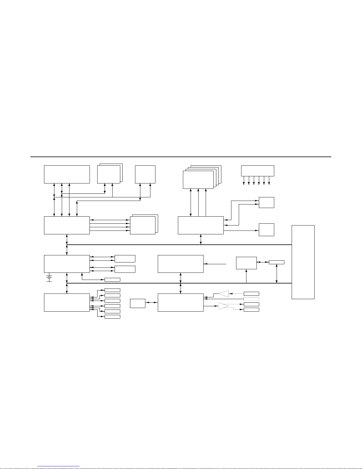
1.3 Block Diagram
IO_DDS (15:0)
IO_DDP (15:0)
SUPER IO
SMC FD37C67X
IC16
PCI - ISA BRIDGE (+RTC)
PIIX4E
IC23
SYSTEM CONTROLLER
430TX MTXC
IC9
C
O
N
T
R
O
L
P_A(31:3)
K_TA(7:0)
CPU
SOCKET 7
IC13
P_D(63:0)
NLX RISER CONNECTOR
AUDIO SYSTEM CONTR.
CS4236B
IC28
SERIAL PORT1
PL3
SERIAL PORT2
PL7
FLOPPY DRIVES
(NLX RISER)
PARALLEL PORT
PL3
EEPROM
24C16
IC22
ISA BUS
I/O CONNECTORS
DUAL USB
PL15
KEYBOARD
PL9
MOUSE
PL9
CONTR.
CONTR.
CONN.
PRIMARY IDE
(NLX RISER)
CONN.
SECONDARY IDE
(NLX RISER)
SYSTEM MONITOR
LM78
IC24
LM4880, IC25
CD IN
PL24 (OR NLX)
HEADPHONE
PL17
INT.SPEAKER
(NLX RISER)
XBUS_XD (7:0)
ISA
_SA
(19:0)
LM358, IC27
MICROPHONE
PL20
IO_LID#,
fan_speed,
power_lines
FLASH BIOS
2Mb
IC15
ISA
_
SD
(15:0)
BUFFER
VIDEO RAM 0,1,2,3
DRAM_256K16
IC26,29,32,34
VIDEO DISPLAY CONTR.
ATI 264VT3
IC10
MEM BANK 0,1
SDRAM DIMM
MM1,MM2
PCI BUS
MEM_MA (11:0)
MEM_CAS# (7:0)
MEM_RAS# (3:0)
MEM_D (63:0)
V
ID
_M
D
(63:0)
V
ID
_M
A
(9:0)
C
O
N
T
R
O
L
TAG
SRAM 32K X 8
IC5
CACHE 0,1
64K X 32
IC7, 11
RGB,SYNC.
VID_PIXEL (7:0)
CONTR.
CONN.
VGA
PL3
CONN.
VFC/AMC
PL12
SYSTEM CLOCKS
ICS9147-03
IC4
2 Electronics
2.1 Processor
Processor support is for a dual voltage-plane socket 7, for the P54C, P55C and K6. Processor
bus speeds allowed are 60 or 66MHz, and all core multipliers can be set from the main jumper
block PL10. Depending on the processor fitted, the processor bus speed, core multiplier, and
core voltage will have to be correctly set.
2.2 Core Logic
This is the Intel 430TX Pentium PCI chipset which comprises the MTXC North Bridge and
the PIIX4E South Bridge, both in BGA packages:
Board Build Part Step Top Marking
Rev A to D MTXC A1 FW82439TX Q536ES (sample)
FW82439TX Q537ES (sample)
FW82439TX SL238 (prodn.)
Rev D MTXC A2 FW82439TX SL28T (prodn.)
Rev A to D PIIX4 B0 FW82371AB Q534ES (sample)
FW82371AB Q535ES (sample)
FW82371AB SL23P (prodn.)
MTXC North Bridge features
64-bit processor host interface, Pentium family at 60MHz and 66MHz
64-bit DRAM controller, 4MB to 256MB main memory, EDO or SDRAM
L2 cache controller, 256KB or 512KB direct-mapped write-back, caches first 64MB main
memory, PBSRAM or DRAM cache
Synchronous 30MHz/33MHz 32-bit PCI 2.1 bus controller
Data path and buffers, three sets of data buffers
Power management features
PIIX4E South Bridge features
PCI 2.1 interface at 30 & 33MHz
ISA bus controller
Extensive power management features including ACPI compliance
IDE controller, two ports four drives, PIO mode 4 and Ultra 33 synchronous DMA mode
Enhanced DMA controllers, with distributed DMA support
Interrupt controllers, with serial interrupt support
System timers
Dual USB 1.0 port controller, 1.5/12 Mbps
SMBus interface
MC146818A compatible real-time clock with 256 bytes of RAM

HU430 NLX Motherboard User Guide 124575UG Revision 2
Mitsubishi Electric PC Division Page 7 of 21
2.3 Level 2 Cache
L2 cache controller is a direct-mapped write-back design. Only the first 64MB of main
memory can be cached. It supports standard PBSRAM (15ns cycle time, 8ns clock to output)
or DRAM-based cache
HU430 supports a 256KB cache size (with 2 pcs of 32K x 32) or a 512KB cache size (with 2
pcs of 64K x 32). Optional fit resistors set the appropriate register configuration bits in the
MTXC at power-on. The cache size and type is a build option.
2.4 Memory
2.4.1 Main Memory
There are two DIMM sockets on board. Each socket is 64-bits wide and can accept EDO or
SDRAM modules. These must be unbuffered types and parity/ECC is not supported. 4Mb,
16Mb and 64Mb EDO DRAM types and 16Mb and 64Mb SDRAM types are supported.
Maximum memory per DIMM is 128MB with a maximum motherboard capacity of 256MB.
When populating memory DIMMs, either socket MM1 or MM2 may be used. In a singleDIMM system it will be easier to fit it into MM1 as another DIMM may be added to MM2 in
the future without having to unplug the module in MM1.
2.4.2 BIOS
There is a single TSOP-40 geometry on the motherboard for the Flash EPROM. This is
suitable for 1Mb, 2Mb or 4Mb parts with 5V or 12V programming voltages.
An optional enable/disable jumper, when placed in the disable position, blocks write cycles to
the Flash. This means that commands and data cannot be written to the device. The boards
will normally be shipped with the jumper absent, and the Flash set in the 'program enable'
position.
The optional 'force recover' jumper sets a bit in a GPI port in the PIIX4 and is read by the
BIOS. This is used to force a recovery situation such that data is read from the recovery disk
in the floppy disk drive. Normally, this jumper is not fitted as a recovery situation is autodetected by the BIOS.
The optional 'unlock boot jumper' enables the boot block to be temporarily unlocked for reprogramming.
HU430 has been designed so that the TSOP part can be programmed during ICT.
2.5 Video
Video controller support:
ATI VT-B (“VT3”) for standard builds
ATI 3D-Rage II+, optional build

HU430 NLX Motherboard User Guide 124575UG Revision 2
Mitsubishi Electric PC Division Page 8 of 21
The video memory comprises 4 pieces of 256Kx16 40-pin SOJ to give a maximum of 2MB
(64-bits wide). Board builds populated with only 1MB (2 pieces) will have two sockets fitted
to enable the memory to be upgraded to 2MB. The memory type is 40ns EDO DRAM.
An AMC (ATI Media Connector) is also fitted; this is a 40-pin (extended) version of the 26way VESA feature connector.
2.6 Audio
The audio system is based on the Crystal CS4236B. It is a single chip audio controller
compatible with Sound Blaster, Sound Blaster Pro and the Windows Sound System.
Audio features:
Plug-and-Play ISA bus interface
16-bit address decode support
Internal FM Synthesis Support
Dual DMA Support w/FIFOs, full duplex operation
Programmable Power Management
Joystick Port and MPU-401 compatible MIDI interface
6 channel Input Mixer.
The audio circuit’s output stage is a National Semiconductor LM4880 stereo power amplifier
(Boomer family). It drives a single mono internal speaker or a stereo headphone output jack.
The amplifier will produce 600 mW RMS for the internal speaker and approximately 65 mW
RMS per channel for stereo headphones (32 impedance). The stereo headphone output is
derived from the stereo output mixer of the audio controller and the internal speaker's signal
is derived from the audio controller's separate mono output stage. In the Windows mixer
panel, it is necessary to un-mute the 'PC Speaker' output as this controls the audio controller's
mono output.
A microphone input jack is provided with phantom power for electret condenser
microphones. An optional CD-ROM audio connector is provided for connecting the internal
CD-ROM drive's audio output into the motherboard sound system.
There is a 16-way header which provides the MIDI and joystick functionality via an optionalfit 15-way D-type cable assembly.
The audio section can be completely de-populated, leaving the conventional PC-Beep. The
PC beep is always available from the small PCB-mounted speaker if the enable jumper is
present. The output of the audio sub-system is never fed to the PCB-mounted speaker.
If the audio sub-system is not fitted, then the PC beep signal is fed up the NLX riser on the
left channel. If the audio sub-system is fitted then the mono speaker output is fed up the NLX
riser on the left channel.
2.7 Standard I/O
The SMC FDC37C675 combo controller provides standard I/O. This comprises the four
functional blocks below. It is packaged in a 100-pin QFP and is fully PC97 and motherboard
Plug-and-Play compliant. It supports three ISA DMA channels and supports a serial interrupt

HU430 NLX Motherboard User Guide 124575UG Revision 2
Mitsubishi Electric PC Division Page 9 of 21
scheme compatible with that of the PIIX4. This allows a wide selection of interrupt channels
for the serial and parallel ports, and the floppy disk controller.
2.7.1 Keyboard and Mouse
This is implemented in an SMC 37C675 device on the motherboard. The keyboard and mouse
controller uses the Phoenix Multikey version 1.40 firmware. PS/2 style keyboard and mouse
ports are provided on the rear panel. This version does not support keyboard/mouse port
swapping.
2.7.2 Floppy Disk Interface
This is implemented in an SMC 37C675 device on the motherboard. Standard 2-mode and 3mode 3½” drives are supported. The 3-mode drive includes the 1.6MB (unformatted) mode
that is popular in Japan; this requires a special OS device driver that installs the 1.6MB mode
floppy disk drive as another system device.
The floppy disk drive signals are routed from the motherboard to the NLX riser and the
floppy disk drive connector is mounted on the NLX riser.
As per the NLX specification, all floppy disk input signals to the motherboard must be pulled
up on the NLX riser.
2.7.3 Serial Ports
This is implemented in an SMC 37C675 device on the motherboard. There are two standard
COM ports which are wired to two standard 9-way D-type connectors on the rear panel. The
maximum Baud rate is 115K bits per second.
2.7.4 Parallel Port
This is implemented in an SMC 37C675 device on the motherboard. This is EPP 1.7/1.9 and
IEE1284 (ECP) compliant and is compatible with a standard (output only) PC parallel port as
well as a bi-directional (PS/2 style) parallel port. There is a 25-way D-type connector on the
rear panel.
2.8 Additional I/O
2.8.1 IDE Disk Controller
This is integrated into the PIIX4E South Bridge device. Two connectors are provided on the
NLX riser allowing two drives per cable. The system BIOS auto-detects the drives fitted and
sets the best signal timing appropriate for the drives. PIIX4E supports up to PIO mode 4
timing and bus master IDE transfers up to 33MBps (ATA33). The total cable length attached
to each connector must not exceed 12" or signal integrity problems may result.

HU430 NLX Motherboard User Guide 124575UG Revision 2
Mitsubishi Electric PC Division Page 10 of 21
2.8.2 Universal Serial Bus (USB)
The controller is integrated into the PIIX4E. Two channels are wired to a dual-stacked USB
connector provided on the rear panel. Optionally, the motherboard may have a single USB
connector on the rear panel with one channel routed to the NLX riser.
2.8.3 System Management Bus (SMBus)
This is a two-wire bi-directional serial bus compatible with I2C. It comprises a bus master
controller for interrogating other devices, and a slave controller enabling it to act as a slave to
other bus masters. Devices that are connected to this bus are:
mai n memory DIMMs
The video controller I
2
C bus is local to the video controller, AMC connector, and VGA
connector.
2.9 Motherboard Power
2.9.1 Regulators
The board has a switched-mode regulator and optionally, a linear regulator. The switchedmode regulator provides the power for the processor core, and also powers the processor I/O
in the case of a non-MMX Pentium. The 3V3 power for the rest of the motherboard is
supplied either by an optional-fit on-board linear regulator or by the NLX power supply fed
via the NLX riser.
Warnings: if the optional-fit linear regulator is fitted on the motherboard then the user must
ensure that:
3V3 is not supplied to the motherboard from an NLX PSU via the NLX riser
No peripheral or card on the riser uses the motherboard-generated 3V3
As the switched-mode regulator always supplies the CPU core, the voltage is selectable on the
main jumper block to cater for different processor core voltages (the motherboard cannot
detect this automatically).
2.9.2 Battery
An IEC-type CR2032 3V lithium coin cell and holder are fitted to the board. Cell capacities in
the range 170mAh to 210mAh are acceptable. This cell typically provides battery backup of
the RTC for five years. The battery can be replaced by the user - the clip needs to be prised
back with a small screwdriver and the battery is lifted up by spring pressure.

HU430 NLX Motherboard User Guide 124575UG Revision 2
Mitsubishi Electric PC Division Page 11 of 21
2.10 Power Management
2.10.1 Global Power States
The ACPI global power states are summarised in the table below. The last three columns
indicate the colour of a tri-colour LED when the red anode is connected to the 'power LED'
signal from the NLX connector. The 'power LED' signal is controlled by the motherboard.
System power
state
AC input PSU main
o/p rails
CPU Green
anode
Red
anode
F/P
LED
MECH. OFF
(G3)
disconnected off off off off off
SOFT-OFF (G2) connected off off off on or off
(build)
red or
off
SLEEPING
(G1/S1)
connected on on: clock
stopped
on on or off
(s/w)
orange
or green
WORKING (G0) connected on full speed or
clock
throttling
on on or off
(s/w)
orange
or green
2.10.2 Power-on Control
On HU430 a GPO port is used to control the state after an AC reconnect, regardless of how
the machine was powered off:
GPO27 Action
Low machine powers-up in SOFT-OFF and waits for a power button press
before going into WORKING state
High machine powers straight into WORKING state
The GPO port bit is set by the BIOS during each power-on sequence to determine the action
to be taken on the next AC reconnect. This setting is retained by a battery-backed latch. If the
battery is replaced then the board always waits for a power button press before going into the
WORKING state; thereafter the board powers-up immediately upon AC reconnect unless the
BIOS sets the GPO low.
2.11 Expansion Slots
The ISA and PCI expansion slots are located on the riser card. The ISA and PCI signals are
routed through an edge connector on one edge of the board which mates with the NLX riser.
As per the NLX specification, the motherboard requires that the PCI signals are correctly
terminated and pulled up on the NLX riser for the motherboard to operate properly.
2.11.1 Industry Standard Architecture (ISA)

HU430 NLX Motherboard User Guide 124575UG Revision 2
Mitsubishi Electric PC Division Page 12 of 21
The PIIX4E can support up to 5 ISA slots on the riser. There are an additional two ISA
‘loads’ used on the motherboard: the audio and super i/o controllers.
2.11.2 Peripheral Component Interconnect (PCI)
The motherboard can support up to 3 bus master PCI slots on the NLX riser.
2.12 Bus Resource Utilisation
2.12.1 ISA DMA Channels
DMA Data
Width
Usual Assignment Audio
Combo
0
8-bit
option
1
8-bit Audio (8-bit)
option option
2
8-bit Floppy disk controller
option
3
8-bit ECP parallel port
option option
4
- DMAC daisy chain
5
16-bit
6
16-bit
7
16-bit
Shaded areas indicate DMA channels not normally available on the ISA bus
2.12.2 ISA Interrupts
IRQ Usual Assignment
Audio Combo
0 Timer 0
1 Keyboard
option
2 PIC daisy chain
option
3 Serial port 2
option
4 Serial port 1
option
5Audio
option option
6 Floppy disk controller
option
7 Parallel port
option option
8 Real-time clock
option
9Video
option option
10
option
11
option option
12 Mouse
option option
13 Co-processor
option
14 Primary IDE
option
15 Secondar y IDE
option option
Shaded areas indicate IRQs not normally available on the ISA bus

HU430 NLX Motherboard User Guide 124575UG Revision 2
Mitsubishi Electric PC Division Page 13 of 21
2.12.3 PCI Interrupts
Channel Device
INTA# Slots
INTB# Slots
INTC# Slots
INTD# Video & slots
2.12.4 PCI Device Selection
Dev No IDSEL Device Function No Function
0 AD(11) MTXC
4 AD(15) VGA
7 AD(18) PIIX4E 0 PCI-ISA bridge
“ “ “ 1 IDE interface
“ “ “ 2 USB interface
“ “ “ 3 Power management
16 AD(27) Slot 3
18 AD(29) Slot 2
20 AD(31) Slot 1
Slot resource depends on NLX riser conforming to NLX specification
2.12.5 PCI Arbitration
Channel Device
PHOLD# PIIX4E
0VGA
1 Slot 1
2 Slot 2
3 Slot 3
3 Electrical, Mechanical, Thermal
3.1 Power Requirements
TBD
3.2 PCB
The PCB is a four-layer design measuring W9.0” x L10.0”. It is designed to be NLX
compatible. The following table shows a size comparison with current MEPCD

HU430 NLX Motherboard User Guide 124575UG Revision 2
Mitsubishi Electric PC Division Page 14 of 21
motherboards. The 'width' dimension is the edge adjacent to the system rear panel which
contains the I/O connectors:
Length Width Comments
Standard LPX 13.0” 9.0”
Spitfire 7.6” 9.0” Small LPX
HU430 10.0" 9.0" Small NLX
3.3 Thermal
The processor site needs to dissipate up to 28.3W. This will accommodate the 233MHz
0.35µm (3.2V) version of K6. The case temperature of Pentium, Pentium MMX or K6
processors must not exceed 70ºC.

HU430 NLX Motherboard User Guide 124575UG Revision 2
Mitsubishi Electric PC Division Page 15 of 21
Appendix A. Jumpers And Switches
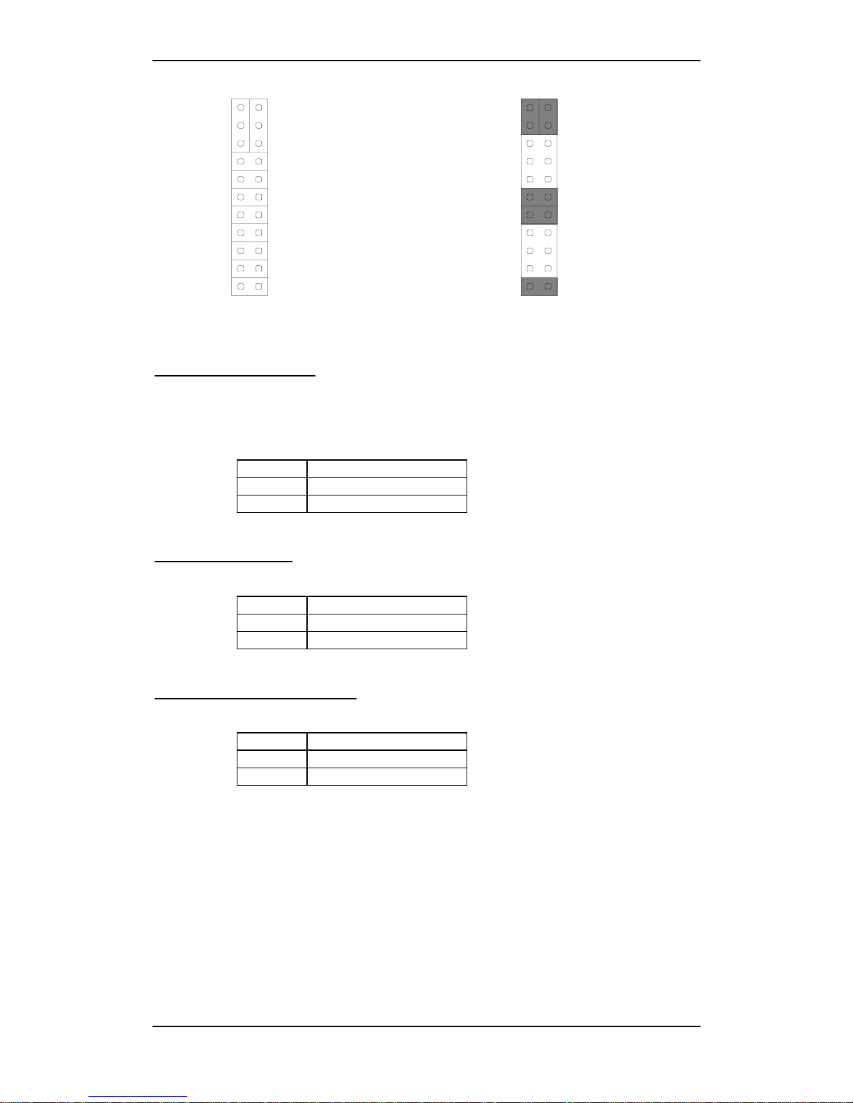
Main Jumper Block, PL10
BF1 and BF0 set the processor bus/core multiplier ratio on P54C and P55C processors, and
BF2 is present to support the K6. The FS jumper selects a processor bus speed of 60 or 66
MHz.
The VGA jumper enables/disables the on-board VGA controller as follows:
VGA = IN Enable on-board VGA controller
VGA = OUT Disable on-board VGA
controller
The AUDIO jumper enables/disables the on-board audio (if fitted) as follows:
AUD = IN Enable on-board audio
AUD = OUT Disable on-board audio
Note that the BIOS auto-detects a video card plugged into an expansion slot and disables the
on-board video. The VGA jumper provided disables the on-board VGA controller in
hardware in case there is a problem with the auto-disable function.
The PW3-0 jumpers select the value of the processor core voltage. This is necessary as P54C,
P55C and K6 processors require different core voltages. The board cannot automatically
detect the core voltage that is required by the processor and so this must be set manually.
The table below shows supported CPUs with their configuration jumper settings; note that the
presence of any processor type or speed in the table does not imply that it is or will be
available:
CPU Core/bus
speeds
Ratio PCI/ISA bus
speeds
BF2 BF1 BF0 FS Pw2 Pw1 Pw0 Pw3 Cor
V
P54C 90/60 MHz 3/2 30/7.5 MHz OUT 1 1 IN IN IN IN IN 3.5
P54C 100/66 MHz 3/2 33/8.33 MHz OUT 1 1 OUT IN IN IN IN 3.5
P54C 120/60 MHz 2/1 30/7.5 MHz OUT 1 0 IN IN IN IN IN 3.5
P54C 133/66 MHz 2/1 33/8.33 MHz OUT 1 0 OUT IN IN IN IN 3.5
P54C 150/60 MHz 5/2 30/7.5 MHz OUT 0 0 IN IN IN IN IN 3.5
P54C 166/66 MHz 5/2 33/8.33 MHz OUT 0 0 OUT IN IN IN IN 3.5
P55C 166/66 MHz 5/2 33/8.33 MHz OUT 0 0 OUT OUT OUT OUT IN 2.8
K6 166/66 MHz 5/2 33/8.33 MHz OUT 0 0 OUT IN OUT OUT IN 3.2
P54C 200/66 MHz 3/1 33/8.33 MHz OUT 0 1 OUT IN IN IN IN 3.5
P55C 200/66 MHz 3/1 33/8.33 MHz OUT 0 1 OUT OUT OUT OUT IN 2.8
K6 200/66 MHz 3/1 33/8.33 MHz OUT 0 1 OUT IN OUT OUT IN 3.2
P55C 233/66 MHz 7/2 33/8.33 MHz OUT 1 1 OUT OUT OUT OUT IN 2.8
K6 0.35µm 233/66 MHz 7/2 33/8.33 MHz OUT 1 1 OUT IN OUT OUT IN 3.2
K6 0.25µm 233/66 MHz 7/2 33/8.33 MHz OUT 1 1 OUT OUT IN OUT OUT 2.2
K6 0.25µm 266/66 MHz 4/1 33/8.33 MHz IN 1 0 OUT OUT IN OUT OUT 2.2
K6 0.25µm 300/66 MHz 9/2 33/8.33 MHz IN 0 0 OUT OUT IN OUT OUT 2.2
HU430 NLX Motherboard User Guide 124575UG Revision 2
Mitsubishi Electric PC Division Page 16 of 21
Example - 233MHz P55C
AUDIO (IN=enable)
VGA (IN=enable)
FS (IN=60MHz, OUT=66MHz)
PL10 - Configuration
=0
BF2
=1
=0
=1
PW3
PW0
PW1
PW2
BF0
BF1
=0
=1
BF1
=0
BF2
=1
PW3
PW0
PW1
PW2
BF0
FS
VGA
AUDIO
MMX Power Jumper PL5
Note that these two jumpers must be fitted for a Pentium MMX or K6 processor to function
correctly.
Position Function
1-2, 3-4 P55C MMX or K6
No fit P54C Pentium
Battery Jumper, PL19
Position Function
1-2 Normal operation
2-3 Clear RTC CMOS RAM
Enable On-board Speaker, PL13
Position Function
IN Enable on-board speaker
OUT Disable

HU430 NLX Motherboard User Guide 124575UG Revision 2
Mitsubishi Electric PC Division Page 17 of 21
Appendix B. Connector Assignments
NLX Riser Edge Connector
TBA
NLX Supplemental Edge Connector
TBA
USB, PL15
1
4
14
USB
Port 0
USB
Port 1
1+5V
2 DATA3 DATA+
4 GND
The +5V supply to both connectors is fused with a single 1.1A resettable fuse.
AMC, PL12
Digital ground 1 2 P0
Digital ground 3 4 P1
Digital ground 5 6 P2
EVIDEO/IOW#78P3
ESYNC/IOR# 9 10 P4
EDCLK/RDY 11 12 P5
NC/SAD4/SDA13 14 P6
Digital ground 15 16 P7
Digital ground 17 18 DCLK
Digital ground 19 20 BLANK#/SA
D0
VFSENSE# 21 22 HSYNC/SAD1
NC/SCL 23 24 VSYNC/SAD2
Key pin 25 26 Digital ground
Key pin 27 28 Key pin

HU430 NLX Motherboard User Guide 124575UG Revision 2
Mitsubishi Electric PC Division Page 18 of 21
+5V 29 30 SAD3
RESET# 31 32 SAD7
SAD6 33 34 SAD5
RES/SDA 35 36 REV
Analogue gnd 37 38 +12V
AUDRIGHT 39 40 AUDLEFT
VGA, PL3
5
15
10
1
6
11
GND NC BLUE GREEN RED
1
GND +5V B RTN G RTN R RTN
6
SCL VSYNC HSYNC SDA NC
11
The +5V supply is fused with a 1.1A resettable fuse.
Keyboard & Mouse, PL9
1CLK
2+5V
3 GND
4 No connect
5 DATA
6 No connect
Parallel Port, PL3
1
14
13
25
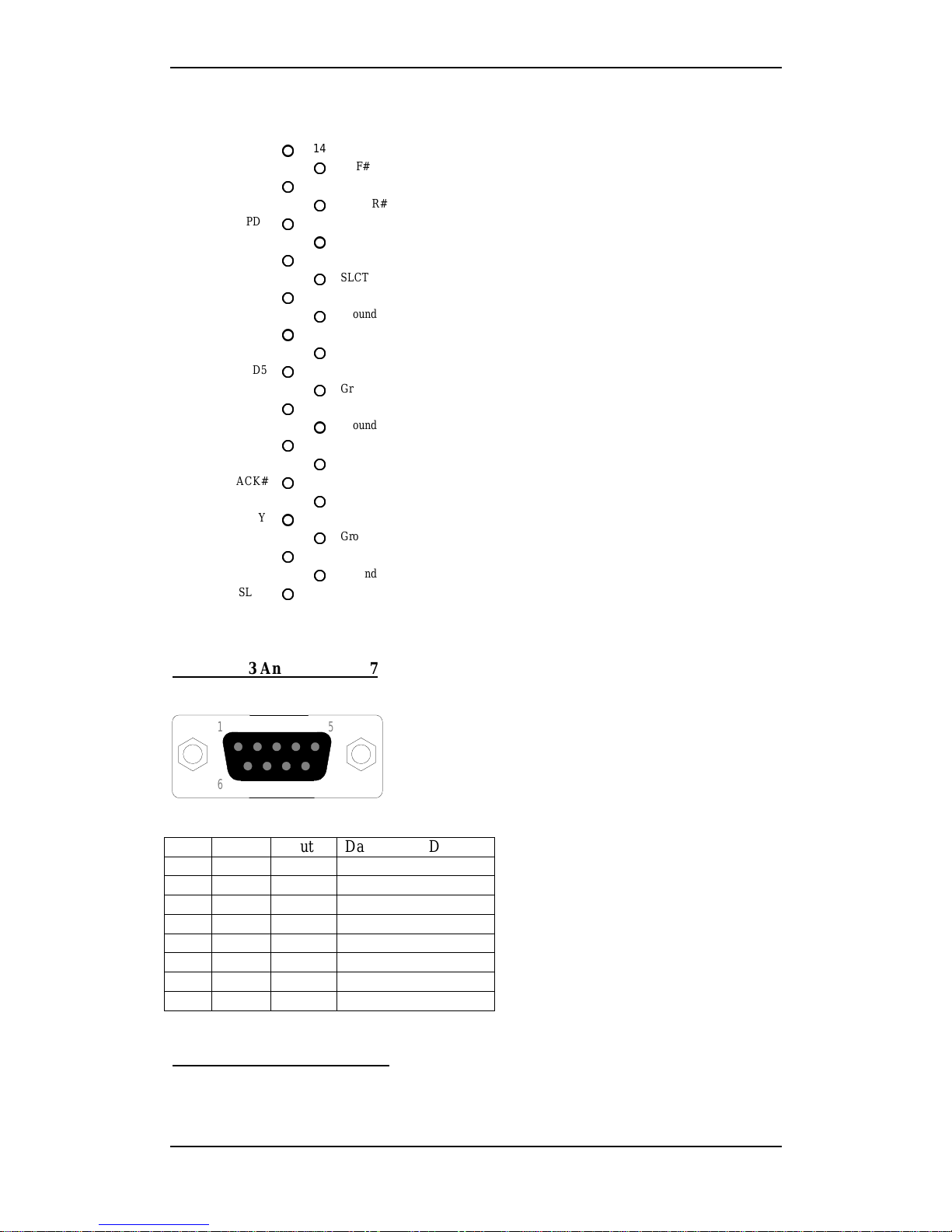
HU430 NLX Motherboard User Guide 124575UG Revision 2
Mitsubishi Electric PC Division Page 19 of 21
1
STROBE#
14
ALF#
PD0
ERROR#
PD1
INIT#
PD2
SLCTIN#
PD3
Ground
PD4
Ground
PD5
Ground
PD6
Ground
PD7
Ground
ACK#
Ground
BUSY
Ground
PE
Ground
SLCT
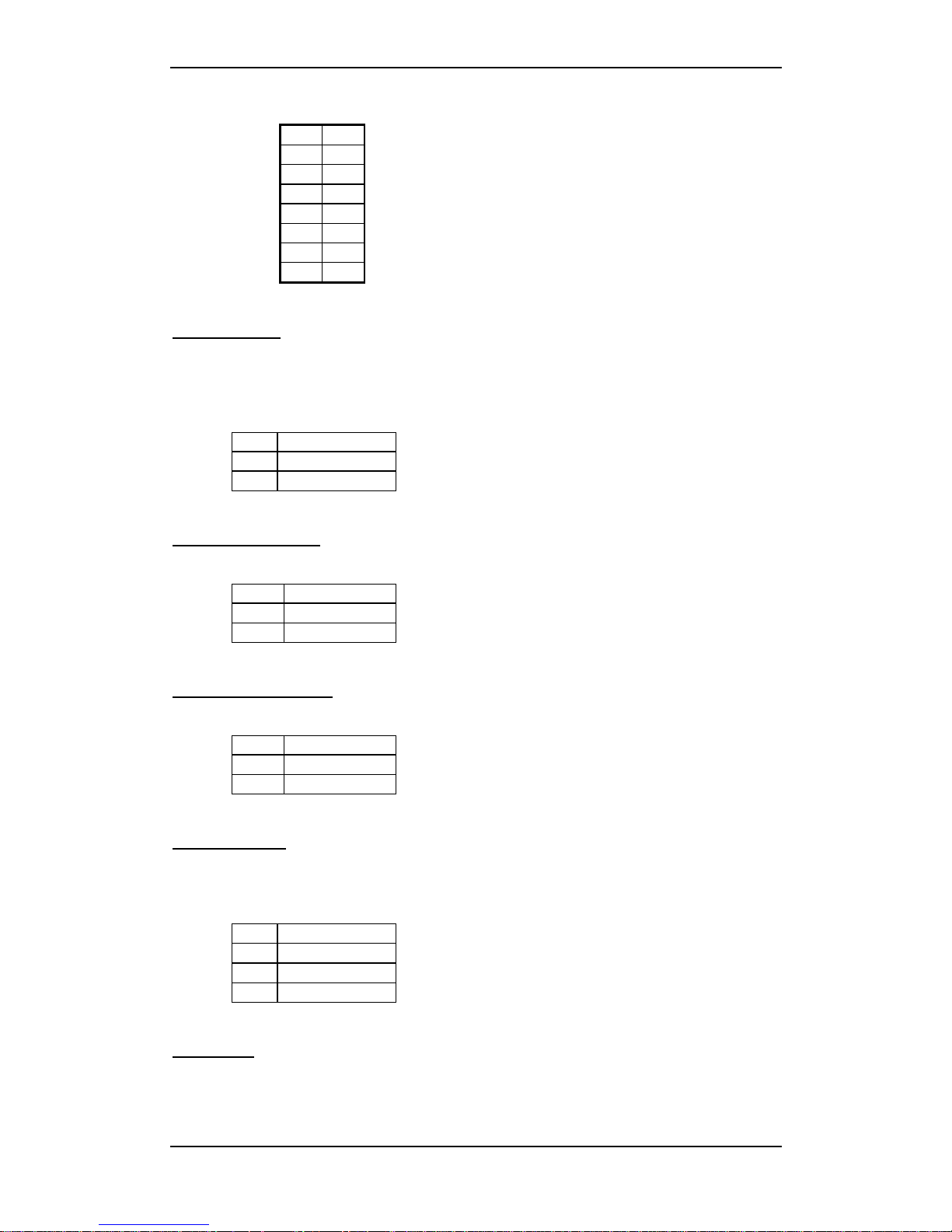
COM1, PL3 And COM2, PL7
1
6
5
9
1 DCD Input Data Carrier Detect
2 RXD Input Receive Data
3 TXD Output Transmit Data
4 DTR Output Data Terminal Ready
5 GND Ground Ground reference pin
6 DSR Input Data Set Ready
7 RTS Output Ready To Send
8 CTS Input Clear To Send
9 RI Input Ring Indicate
MIDI & Joystick Header, PL18
The +5V supply to this connector is fused with a 1.1A resettable fuse.
HU430 NLX Motherboard User Guide 124575UG Revision 2
Mitsubishi Electric PC Division Page 20 of 21
+5V 1 2 +5V
J/stick A fire 1 3 4 J/stick B fire 1
J/stick A x-ctrl 5 6 J/stick B x-ctrl
GND 7 8 MIDI out
GND 9 10 J/stick B y-ctrl
J/stick A y-ctrl 11 12 J/stick B fire 2
J/stick A fire 2 13 14 MIDI in
+5V 15 16 Key pin
CPU Fan, PL16
The fan output is fused with a 0.75A resettable fuse. The maximum continuous current that
can be supplied by the motherboard is 150mA.
1 Ground
2 +12V switched
3 Ground
Microphone In, PL20
Shld Frame GND
Ring Bias
Tip Signal input
Headphones Out, PL17
Shld Frame GND
Ring Right output
Tip Left output
CD Audio, PL24
This connector is not always fitted to the motherboard.
1 Reference
2 Left in
3 Reference
4 Right in
Reset, PL14
This connector is not always fitted to the motherboard.

HU430 NLX Motherboard User Guide 124575UG Revision 2
Mitsubishi Electric PC Division Page 21 of 21
To cause a reset event to occur, pin 1 must be shorted to ground.
1 Input
2 Ground
 Loading...