

Page 1

COLOR MONITOR
E55LCD
MODEL No. NL1503 (B)
200208
08R220B3
SERVICE MANUAL
PART NO. 599910610
NEC-MITSUBISHI ELECTRIC VISUAL SYSTEMS CORPORATION
AUGUST 2002
Page 2
WARNING
The SERVICE PERSONNEL should have the appropriate technical training, knowledge and experience
necessary to:
• Be familiar with specialized test equipment, and
• Be careful to follow all safety procedures to minimize danger to themselves and their coworkers.
To avoid electrical shocks, this equipment should be used with an appropriate power cord.
This equipment utilized a micro-gap power switch. Turn off the set by first pushing power switch. Next,
remove the power cord from the AC outlet.
To prevent fire or shock hazards, do not expose this unit to rain or moisture.
This symbol warns the personnel that un-insulated voltage within the unit may have sufficient
magnitude to cause electric shock.
This symbol alerts the personnel that important literature concerning the operation and
maintenance of this unit has been included.
Therefore, it should be read carefully in order to avoid any problems.
PRODUCT SAFETY CAUTION
1. When parts replacement is required for servicing, always use the manufacturer's specified replacement.
2. When replacing the component, always be certain that all the components are put back in the place.
3. As for a connector, pick and extract housing with fingers properly since a disconnection and improper
contacts may occur, when wires of the connector are led.
4. Use a proper screwdriver. If you use screwdriver that does not fit, you may damage the screws.
Page 3

CONTENTS
Page No.
USER'S MANUAL ------------------------------------------------------------------- 1-1
SERIAL NUMBER INFORMATION --------------------------------------------- 2-1
DISASSEMBLY ----------------------------------------------------------------------- 3-1
ADJUSTMENT PROCEDURES -------------------------------------------------- 4-1
INSPECTION --------------------------------------------------------------------------- 5-1
TROUBLE SHOOTING ------------------------------------------------------------- 6-1
CIRCUIT DESCRIPTION ----------------------------------------------------------- 7-1
REPLACEMENT PARTS LIST --------------------------------------------------- 8-1
BLOCK DIAGRAM ------------------------------------------------------------------- 9-1
SCHEMATIC DIAGRAMS -------------------------------------------------------- 10-1
Page 4
1-1
User's Manual
www.nec-mitsubishi.com
Page 5
1-2
FCC Statement
This device complies with Part 15 of FCC Rules. Operation is subject to the following two conditions. (1) This device may not
cause harmful interference, and (2) this device must accept any interference received, including interference that may cause
undesired operation.
U.S. Responsible Party: NEC-Mitsubishi Electronics Display of America, Inc.
Address: 1250 North Arlington Heights Road, Suite 500
Itasca, Illinois 60143-1248
Tel. No.: (630) 467-3000
Type of Product: Computer Monitor
Equipment Classification: Class B Peripheral
Model: M6JNL1503
For the Customer to use in U.S.A. or Canada
Canadian Department of Communications Compliance Statement
DOC: This Class B digital apparatus meets all requirements of the Canadian Interference-Causing Equipment Regulations.
Cet appareil numérique de la classe B respecte toutes les exigences du Règlement sur le matériel brouiller du Canada.
C-UL: Bears the C-UL Mark and is in compliance with Canadian Safety Regulations according to CSA C22.2 #950.
Ce produit porte la marque ‘C-UL’ et se conforme aux règlements de sûrele Canadiens selon CAN/CSA C22.2 No. 950.
FCC Information
1. Use the attached specified cables with the LCD monitor colour monitor so as not to interfere with radio and television
reception.
(1) The power supply cord you use must have been approved by and comply with the safety standards of U.S.A. &
Europe, and meet the following condition.
Power supply cord Non shield type, 2-power cord
Length conductor (2 m)
Plug shape
U.S.A Continental Europe
(2) Shielded video signal cable. Use of other cables and adapters may cause interference with radio and television
reception.
2. This equipment has been tested and found to comply with the limits for a Class B digital device, pursuant to part 15 of
the FCC Rules. These limits are designed to provide reasonable protection against harmful interference in a residential
installation. This equipment generates, uses, and can radiate radio frequency energy, and, if not installed and used in
accordance with the instructions, may cause harmful interference to radio communications. However, there is no
guarantee that interference will not occur in a particular installation. If this equipment does cause harmful interference
to radio or television reception, which can be determined by turning the equipment off and on, the user is encouraged
to try to correct the interference by one or more of the following measures:
• Reorient or relocate the receiving antenna.
• Increase the separation between the equipment and receiver.
• Connect the equipment into an outlet on a circuit different from that to which the receiver is connected.
• Consult your dealer or an experienced radio/TV technician for help.
Changes or modifications not expressly approved by the party responsible for complicance could void the user’s
authority to operate the equipment.
If necessary, the user should contact the dealer or an experienced radio/television technician for additional
suggestions. The user may find the following booklet, prepared by the Federal Communications Commission, helpful:
“How to Identify and Resolve Radio-TV Interference Problems.” This booklet is available from the U.S. Government
Printing Office, Washington, D.C., 20402, Stock No. 004-000-00345-4.
Page 6

1-3
Congratulations! You have just purchased a
TCO’99 approved and labeled product! Your choice
has provided you with a product developed for
professional use. Your purchase has also
contributed to reducing the burden on the
environment and also to the further development of
environmentally adapted electronics products.
Why do we have environmentally labelled computers?
In many countries, environmental labelling has become an
established method for encouraging the adaptation of goods and
services to the environment. The main problem, as far as
computers and other electronics equipment are concerned, is that
environmentally harmful substances are used both in the products
and during the manufacturing. Since it has not been possible for
the majority of electronics equipment to be recycled in a
satisfactory way, most of these potentially damaging substances
sooner or later enter Nature.
There are also other characteristics of a computer, such as energy
consumption levels, that are important from the viewpoints of both
the work (Internal) and natural (external) environments. Since all
methods of conventional electricity generation have a negative
effect on the environment (acidic and climate-influencing
emissions, radioactive waste, etc.), it is vital to conserve energy.
Electronics equipment in offices consume an enormous amount
of energy since they are often left running continuously.
What does labelling involve?
This product meets the requirements for the TCO’99 scheme
which provides for international and environmental labelling of
personal computers. The labelling scheme was developed as a
joint effort by the TCO (The Swedish Confederation of Professional
Employees), Svenska Naturskyddsforeningen (The Swedish
Society for Nature Conservation) and Statens Energimyndighet
(The Swedish National Energy Administration).
The requirements cover a wide range of issues: environment,
ergonomics, usability, emission of electrical and magnetic fields,
energy consumption and electrical and fire safety.
The environmental demands concern restrictions on the presence
and use of heavy metals, brominated and chlorinated flame
retardants, CFCs (freons) and chlorinated solvents, among other
things. The product must be prepared for recycling and the
manufacturer is obliged to have an environmental plan which must
be adhered to in each country where the company implements its
operational policy. The energy requirements include a demand that
the computer and/or display, after a certain period of inactivity,
shall reduce its power consumption to a lower level in one or more
stages. The length of time to reactivate the computer shall be
reasonable for the user.
Labelled products must meet strict environmental demands, for
example, in respect of the reduction of electric and magnetic fields,
physical and visual ergonomics and good usability.
Environmental Requirements
Flame retardants
Flame retardants are present in printed circuit boards, cables,
wires, casings and housings. In turn, they delay the spread of fire.
Up to thirty percent of the plastic in a computer casing can consist
of flame retardant substances. Most flame retardants contain
bromine or chloride and these are related to another group of
environmental toxins, PCBs, which are suspected to give rise to
severe health effects, including reproductive damage in fisheating
birds and mammals, due to the bio-accumulative* processes.
Flame retardants have been found in human blood and
researchers fear that disturbances in foetus development may
occur.
TCO’99 demand requires that plastic components weighing more
than 25 grams must not contain flame retardants with organically
bound chlorine and bromine. Flame retardants are allowed in the
printed circuit boards since no substitutes are available.
Lead**
Lead can be found in picture tubes, display screens, solders and
capacitors. Lead damages the nervous system and in higher
doses, causes lead poisoning.
TCO’99 requirement permits the inclusion of lead since no
replacement has yet been developed.
Cadmium**
Cadmium is present in rechargeable batteries and in the
colourgenerating layers of certain computer displays. Cadmium
damages the nervous system and is toxic in high doses.
TCO’99 requirement states that batteries, the colourgenerating
layers of display screens and the electrical or electronics
components must not contain any cadmium.
Mercury**
Mercury is sometimes found in batteries, relays and switches,
Mercury damages the nervous system and is toxic in high doses.
TCO’99 requirement states that batteries may not contain any
Mercury. It also demands that no mercury is present in any of
the electrical or electronics components associated with the
display unit.
CFCs (freons)
CFCs (freons) are sometimes used for washing printed circuit
boards. CFCs break down ozone and thereby damage the ozone
layer in the stratosphere, causing increased reception on Earth
of ultraviolet light with consequent increased risks of skin cancer
(malignant melanoma).
The relevant TCO’99 requirement; Neither CFCs nor HCFCs
may be used during the manufacturing and assembly of the
product or its packaging.
*Bio-accumulative is defined as substances which accumulate
within living organisms.
**Lead, Cadmium and Mercury are heavy metals which are
Bio-accumulative.
To obtain complete information on the environmental criteria
document, order from:
TCO Development Unit
SE-114 94 Stockholm
SWEDEN
FAX Number: +46 8 782 92 07
E-mail (Internet): development@tco.se
You may also obtain current information on TCO’99 approved
and labelled products by visiting their website at:
http://www.tcodevelopment.com
TCO’99
Page 7

1-4
Index
Warning, Caution .................................... English-1
Declaration ............................................. English-1
Contents ................................................. English-2
Quick Start .............................................. English-2
Controls .................................................. English-5
Recommended Use ................................ English-7
Specifications ......................................... English-8
Features ................................................. English-9
Troubleshooting .................................... English-10
Varování, Upozornûní ............................... âesky-1
Prohlá‰ení ................................................ âesky-1
Obsah ....................................................... âesky-2
Rychl˘ start ............................................... âesky-2
Ovládací prvky .......................................... âesky-5
Provozní pokyny ....................................... âesky-7
Technické údaje........................................ âesky-8
Vlastnosti .................................................. âesky-9
OdstraÀování problémÛ .......................... âesky-10
Warnung, Vorsicht ................................. Deutsch-1
Erklärung ............................................... Deutsch-1
Inhalt der Verpackung ............................Deutsch-2
Kurzanleitung......................................... Deutsch-2
Bedienelemente .................................... Deutsch-5
Einsatzempfehlungen ............................Deutsch-7
Technische Daten .................................. Deutsch-8
Merkmale und Funktionen .....................Deutsch-9
Fehlerbehebung .................................. Deutsch-10
ΠΡΟΕΙ∆ΟΠΟΙΗΣΗ, ΠΡΟΣΟΧΗ.......... Ελληνικά-1
∆ήλωση .............................................. Ελληνικά-1
Περιεχµενα ..................................... Ελληνικά-2
Γρήγορη Εκκίνηση ............................Ελληνικά-2
Πλήκτρα Ελέγχου .............................Ελληνικά-5
Συνιστώµενη χρήση ......................... Ελληνικά-7
Προδιαγραφές .................................. Ελληνικά-8
Χαρακτηριστικά ................................ Ελληνικά-9
Εντοπισµς Βλαβών ....................... Ελληνικά-10
Advertencia, Peligro .............................. Español-1
Declaración ........................................... Español-1
Contenido .............................................. Español-2
Inicio rápido ........................................... Español-2
Controles ............................................... Español-5
Uso recomendado ................................. Español-7
Especificaciones .................................... Español-8
Características ...................................... Español-9
Solución de problemas ........................ Español-10
Avertissement, Attention....................... Français-1
Déclaration ........................................... Français-1
Contenu ................................................ Français-2
Mise en marche rapide ......................... Français-2
Commandes ......................................... Français-5
Conseils d’utilisation ............................. Français-7
Spécifications ....................................... Français-8
Fonctionnalités ..................................... Français-9
Résolution des problèmes .................. Français-10
Avvertenza, Attenzione........................... Italiano-1
Dichiarazione .......................................... Italiano-1
Contenuto ............................................... Italiano-2
Guida rapida ........................................... Italiano-2
Comandi ................................................. Italiano-5
Raccomandazioni per l’uso .................... Italiano-7
Specifiche tecniche ................................ Italiano-8
Caratteristiche ........................................ Italiano-9
Soluzione dei problemi più comuni ....... Italiano-10
Waarschuwing, Let op! .................... Nederlands-1
Kennisgeving ................................... Nederlands-1
Inhoud ............................................. Nederlands-2
Snel aan de slag .............................. Nederlands-2
Besturingselementen ....................... Neder lands-5
Aanbevolen gebruik ......................... Neder lands-7
Specificaties .................................... Nederlands-8
Eigenschappen ................................ Neder lands-9
Problemen oplossen ...................... Neder lands-10
Uwagi dotyczàce zasilania monitora ........ Polski-1
Ostrze˝enie, Uwaga ................................. Polski-2
Deklaracja ................................................ Polski-2
ZawartoÊç opakowania ............................. Polski-3
Pod∏àczenie monitora ............................... Polski-3
Przyciski ................................................... Polski-6
Zalecenia eksploatacyjne ......................... Polski-8
Dane techniczne ....................................... Polski-9
Cechy charakterystyczne ....................... Polski-10
Usuwanie usterek ................................... Polski-11
Предупреждение, Внимание ............. Русский-1
Заявление ........................................... Русский-1
Содержимое........................................ Русский-2
Краткое руководство
по началу работы ............................... Русский-2
Органы управления ............................ Русский-5
Рекомендации по эксплуатации ........ Русский-7
Технические характеристики ............ Русский-8
Характеристики .................................. Русский-9
Устранение неисправностей ........... Русский-10
D∂kkat, Uyari ............................................ Türkçe-1
Bildirim ..................................................... Türkçe-1
∑çindekiler ................................................ Türkçe-2
H∂zl∂ Baµlama .......................................... Türkçe-2
Kontroller ................................................. Türkçe-5
Tavsiye edilen kullan∂m ........................... Türkçe-7
Teknik Özellikler ...................................... Türkçe-8
Özellikler .................................................. Türkçe-9
Sorun Giderme ...................................... Türkçe-10
Page 8
1-5
English
âesky
Deutsch
Ελληνικά
Español
Français
Italiano
Nederlands
Polski
Русский
Türkçe
Page 9
1-6
English
English-1
Declaration
Declaration of the Manufacturer
TO PREVENT FIRE OR SHOCK HAZARDS, DO NOT EXPOSE THIS UNIT TO RAIN OR MOISTURE. ALSO, DO NOT
USE THIS UNIT’S POLARIZED PLUG WITH AN EXTENSION CORD RECEPTACLE OR OTHER OUTLETS UNLESS
THE PRONGS CAN BE FULLY INSERTED.
REFRAIN FROM OPENING THE CABINET AS THERE ARE HIGH VOLTAGE COMPONENTS INSIDE. REFER
SERVICING TO QUALIFIED SERVICE PERSONNEL.
WARNING
CAUTION
CAUTION: TO REDUCE THE RISK OF ELECTRIC SHOCK, DO NOT REMOVE COVER (OR BACK). NO USER
SERVICEABLE PARTS INSIDE. REFER SERVICING TO QUALIFIED SERVICE PERSONNEL.
This symbol warns user that uninsulated voltage within the unit may have sufficient magnitude to cause
electric shock. Therefore, it is dangerous to make any kind of contact with any part inside this unit.
This symbol alerts the user that important literature concerning the operation and maintenance of this unit
has been included. Therefore, it should be read carefully in order to avoid any problems.
RISK OF ELECTRIC SHOCK • DO NOT OPEN
E
NERGY STAR
®
is a U.S. registered trademark.
As an E
NERGY STAR
Partner, NEC-Mitsubishi Electric Visual Systems Corporation has determined that this product meets the
E
NERGY STAR
guidelines for energy efficiency. The E
NERGY STAR
emblem does not represent EPA endorsement of any product or
service.
All other trademarks mentioned in this manual are the property of their respective owners.
IBM PC/XT/AT, PS/2, MCGA, VGA, 8514/A and XGA are registered trademarks of International Business Machines
Corporation.
Apple and Macintosh are registered trademarks of Apple Computer Inc.
Microsoft and Windows are registered trademarks of the Microsoft Corporation.
NEC is a registered trademark of NEC Corporation.
All other trademarks or registered trademarks are property of their respective owners.
We hereby certify that the colour monitor NL1503
is in compliance with
Council Directive 73/23/EEC:
– EN 60950
Council Directive 89/336/EEC:
– EN 55022
– EN 61000-3-2
– EN 61000-3-3
– EN 55024
and marked with
NEC-Mitsubishi Electric Visual
Systems Corporation
4-13-23, Shibaura,
Minato-Ku
Tokyo 108-0023, JAPAN
Caution:
When operating the LCD Monitor with a 100-240V AC power source in Europe, use the power cord provided with the monitor.
In the UK, a BS approved power cord with a moulded plug has a Black (five Amps) fuse installed for use with this equipment.
If a power cord is not supplied with this equipment please contact your supplier.
When operating the LCD Monitor with a 100-240V AC power source in Australia, use the power cord provided with the
monitor.
For all other cases, use a power cord that matches the AC voltage of the power outlet and has been approved by and
complies with the safety standard of your particular country.
Page 10
1-7
English-2
Contents
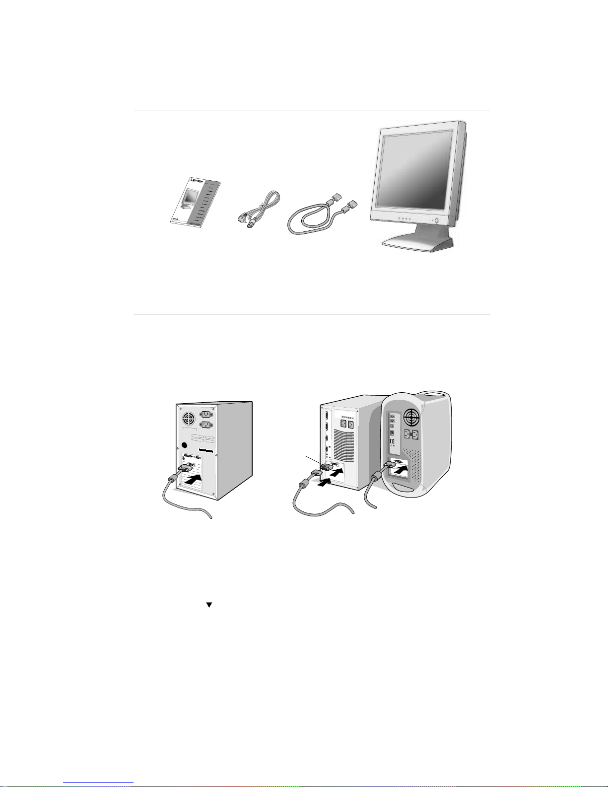
Your new LCD monitor box* should contain the following:
• LCD Monitor with tilt base
• Power cord
• Video Signal Cable (D-SUB to D-SUB Cable)
• User’s Manual
Power Cord
Video Signal Cable
(D-SUB to D-SUB Cable)
User’s Manual
* Remember to save your original box and packing material to transport or ship the monitor.
Quick Start
To attach the LCD monitor to your system, follow these instructions:
1. Turn off the power to your computer.
2. For the PC with Analog output: Connect the 15-pin mini D-SUB to D-SUB signal cable to the connector of the display
card in your system (Figure A.1).
For the Mac: Connect the Macintosh cable adapter (not included) to the computer (Figure B.1).
Attach the 15-pin mini D-SUB signal cable to the MultiSync Macintosh cable adapter (Figure B.1).
NOTE: Some Macintosh systems do not require a Macintosh cable adapter.
Figure A.1
Figure B.1
Mac Adapter
(not included)
Macintosh G3 and G4
do not require an
adapter
3. Remove connector cover. Connect the D-SUB signal cable to the connector on the back of the monitor. Place the video
signal cable (Figure C.1). Replace connector cover.
NOTE: Incorrect cable connections may result in irregular operation, damage display quality/components of LCD module
and/or shorten the module’s life.
4. Remove connector cover. Connect one end of the power cord to the AC inlet on the back of the monitor and the other end
to the power outlet (Figure D.1). Replace the power cord cover.
5. Press an arrow point “
” portion with take off connector cover.
NOTE: Please refer to Caution section of this manual for proper selection of AC power cord.
Page 11
1-8
English
English-3
Figure C.1
Input1
Figure D.1
Input2
Power Cord
Connector Cover
Power Cord
Signal cable
Signal cable
Press an arrow point “
”
portion with take off
Figure E.1
Power switch
6. Turn on the monitor with the Power Button (Figure E.1) and the computer.
7. To complete the setup of your LCD monitor, use the following OSD controls:
• Auto Adjust Contrast (Analog input only)
• Auto Adjust (Analog input only)
Refer to the Controls section of this User’s Manual for a full description of these OSD controls.
NOTE: If you have any problems, please refer to the Troubleshooting section of this User’s Manual.
Tilt
Grasp both sides of the monitor screen with your hands and adjust the tilt as desired (Figure F.1).
The movable scope for elevation and depression of LCD is -5°~30° angle (Figure F.2).
Figure F.1
Figure F.2
Page 12
1-9
English-4
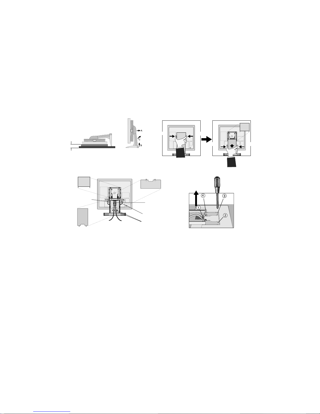
Remove Monitor Stand for Mounting
To prepare the monitor for alternate mounting purposes:
1. Place monitor face down on a non-abrasive surface (Place the screen on a 36 mm platform so that the stand is parallel
with the surface.) (Figure G.1).
2. Displace connector cover on the black of the monitor (Figure G.2).
3. To take off back cover, please follow the instructions of arrow while pressing two side of monitor (Figure G.3).
Next, lift up the stand, dismantle upper cover, then go on to dismantle the stand cover (Figure G.4).
Return the stand to its original position, remove the 4 screws that connect the monitor to the stand, and lift off the stand
assembly (Figure G.5).
4. Disconnect all cables.
5. Reverse this process to reattach stand.
NOTE: Use only VESA-compatible alternative mounting method.
36mm
Figure G.1 Figure G.2
Figure G.3
Figure G.4
PUSH PUSH
PUSHPUSH
AC power cord
1. Cable pass through
in this hole.
2. Connect each
connector.
Signal cable
Clip
To power outlet To computer
Caution: Please use the attached screws (4pcs) when mounting. To fulfil the safety requirements the monitor must be
mounted to an arm which guaranties the necessary stability under consideration of the weight of the monitor. The
LCD monitor shall only be used with an approved arm (e.g. GS mark).
Figure G.5
Page 13
1-10
English
English-5
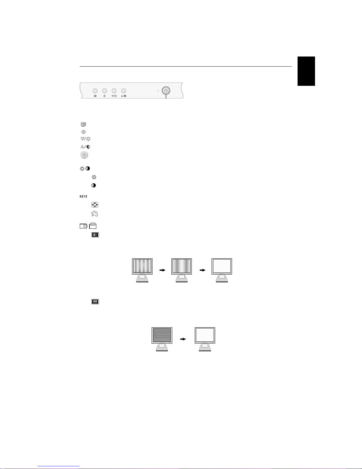
Controls
OSD (On-Screen-Display) Controls
The OSD controls on the front of the monitor function as follows:
To access OSD press any of the control buttons. To change D-SUB signal input, auto detect.
Brightness/Contrast Controls
BRIGHTNESS: Adjusts the overall image and background screen brightness.
CONTRAST: Adjusts the image brightness in relation to the background.
Auto Adjust
Auto Adjust: Automatically adjust the Image Position, the H.Size and Fine setting.
White Balance: Automatically adjust the image for white balance.
H-SIZE
Clock: Adjust the Horizontal size by increasing or decreasing the setting. Should the “Auto Adjust” function do
not give you a satisfactory pictire setting, a further tuning can beperformed using the “H-Size” function (dot
clock). For this Moiré test patten could be used. This function may alter the width of the picture. Use Up/Down
Menu to center the image on the screen. If the H-Size is wrongly calibrated, the result would look like on the left
drawing. The image should be homogeneous.
Phase: Improve focus, clarity and image stability by increasing or decreasing this setting. Should the “Auto
Adjust” function and the “H.Size” function do not give you satisfactory picture setting, a fine tuning can be
performed using the “Fine” function. It improve focus, clearity and image stability by increasing or decreasing
this setting. For this a Moiré test pattern could be used. If the Fine value is wrongly calibrated the result would
look like on the left drawing. The image should be homogeneous.
When no OSD DisplaySwitch Function
Select to next menuOpen menu
Control
Select to next itemAuto-Adjust (Hot key)
Press for adjustment of brightnessBrightness (Hot key) / Decrease
Press for adjustment of contrastContrast (Hot key) / Increase
Switch change to power mode (Power ON/ Power OFF)
Power key
When H.SIZE
value is wrong.
When H.SIZE
value is improved.
When H.SIZE
value is correct.
When PHASE
value is wrong.
When PHASE
value is correct.
Page 14
1-11
English-6
LEFT/RIGHT: Controls Horizontal Image Position within the display area of the LCD.
DOWN/UP: Controls Vertical Image Position within the display area of the LCD.
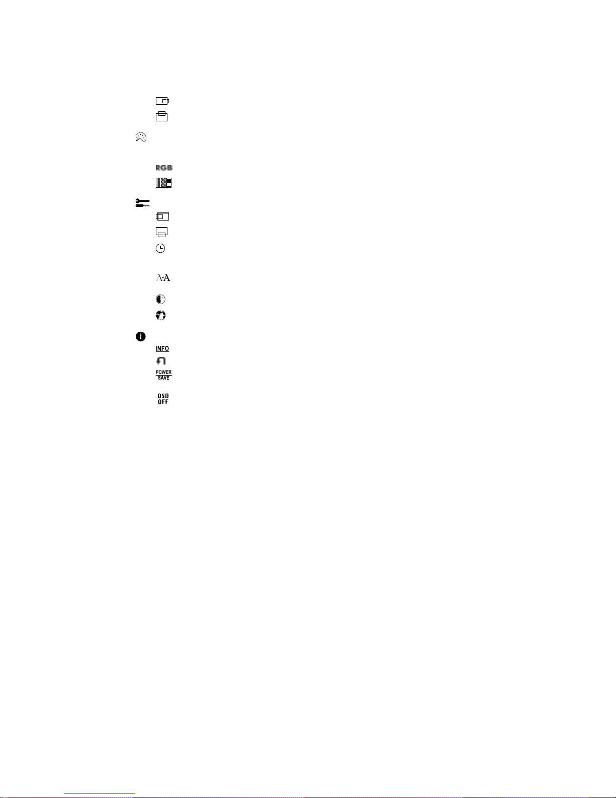
Colour Control Systems
Six colour presets select the desired colour setting.
Colour temperature increases or decreases in each preset.
RGB Grain: Colour grain can be further managed by R.G.B. for desired saturation.
Color-Temperature: Adjust the color temperature at the display. (9300K, 8200K, 7500K, 6500K, 5000K, USER)
Tools
OSD H-POS.: The horizontal image is expanded to approximately 2 times.
OSD V-POS.: The vertical image is changeable.
OSD TURN OFF: The OSM control menu will stay on as long as it is use. In the OSM Turn Off submenu, you
can select how long the monitor waits after the last touch of a button to shut off the OSM control menu. The
preset choices are 5, 10, 15, 20, 25, 30, 35, 40, 45, 50, 55, 60, 120 and 180 seconds.
SHARPNESS: This function is digitally capable to keep crisp image at any timings. It is continuously adjustable
to get distinct image or soft one as you prefer, and set independently by different timings.
OSD TRANSPARENCY: This function allows you to set OSD transparency gradually.
LANGUAGE: OSD control menus are available in seven languages.
INFORMATION
MONITOR INFO: Indicates the model and serial numbers of your monitor.
ALL RESET: Selecting ALL RESET allows you to reset all OSD control settings back to the factory settings.
POWER SAVE: When No signal window appears, select “Power save” to Yes for DPMS function otherwise
system acts in burn-in mode.
NOTE:
AUTO ADJUST (ANALOG INPUT ONLY): Exits the OSD control and main menu.
OSD Warning
NO SIGNAL: This function gives a warning when there is no Horizontal or Vertical Sync Signal present and advises
you to check all Video Inputs on the monitor and computer to make sure they are properly connected. After power is
turned on or when there is a change of input signal or video is inactive, the No Signal window will appear.
OUT OF RANGE: This function gives a recommendation of the optimized resolution and refresh rate. After the power is
turned on or there is a change of input signal or the video signal doesn’t have proper timing, the Out Of Range menu
will appear.
Page 15
1-12
English
English-7
Recommended use
Safety Precautions and Maintenance
FOR OPTIMUM PERFORMANCE, PLEASE NOTE
THE FOLLOWING WHEN SETTING UP AND USING
THE MULTISYNC LCD COLOUR MONITOR:
• DO NOT OPEN THE MONITOR. There are no user serviceable parts inside and opening or removing covers may expose
you to dangerous shock hazards or other risks. Refer all servicing to qualified service personnel.
• Do not spill any liquids into the cabinet or use your monitor near water.
• Do not insert objects of any kind into the cabinet slots, as they may touch dangerous voltage points,which can be harmful
or fatal or may cause electric shock,fire or equipment failure.
• Do not place any heavy objects on the power cord. Damage to the cord may cause shock or fire.
• Do not place this product on a sloping or unstable cart, stand or table, as the monitor may fall, causing serious damage to
the monitor.
• Do not place any objects onto the monitor and do not use the monitor outdoors.
• The inside of the flourescent tube located within the LCD monitor contains mercury. Please follow the bylaws or rules of
your municipality to dispose of the tube properly.
Immediately unplug your monitor from the wall outlet and refer servicing to qualified service personnel under the following
conditions:
• When the power supply cord or plug is damaged.
• If liquid has been spilled, or objects have fallen into the monitor.
• If the monitor has been exposed to rain or water.
• If the monitor has been dropped or the cabinet damaged.
• If the monitor does not operate normally by following operating instructions.
• Do not bend power cord.
• Do not use monitor in high temperatured, humid, dusty, or oily areas.
• Do not cover vent on monitor.
• If monitor is broken, do not come in contact with the liquid crystal.
• If glass is broken. Handle with care.
• Allow adequate ventilation around the monitor so that heat can properly dissipate. Do not block
ventilated openings or place the monitor near a radiator or other heat sources. Do not put anything on
top of monitor.
• The power cable connector is the primary means of detaching the system from the power supply. The
monitor should be installed close to a power outlet which is easily accessible.
• Handle with care when transporting. Save packaging for transporting.
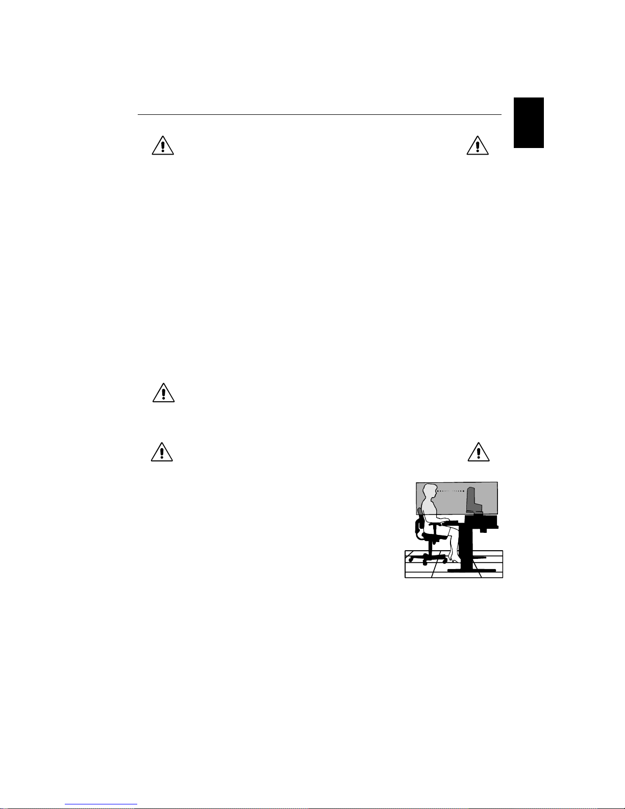
CORRECT PLACEMENT AND ADJUSTMENT OF THE MONITOR
CAN REDUCE EYE, SHOULDER AND NECK FATIGUE. CHECK
THE FOLLOWING WHEN YOU POSITION THE MONITOR:
• For optimum performance, allow 20 minutes for warm-up.
• Adjust the monitor height so that the top of the screen is at or slightly below eye level.
Your eyes should look slightly downward when viewing the middle of the screen.
• Position your monitor no closer than 40 cm and no further away than 70 cm from your
eyes. The optimal distance is 58 cm.
• Rest your eyes periodically by focusing on an object at least 6 m away. Blink often.
• Position the monitor at a 90° angle to windows and other light sources to minimise
glare and reflections. Adjust the monitor tilt so that ceiling lights do not reflect on your
screen.
• If reflected light makes it hard for you to see your screen, use an anti-glare filter.
• Clean the LCD monitor surface with a lint-free, non-abrasive cloth. Avoid using any
cleaning solution or glass cleaner!
• Adjust the monitor’s brightness and contrast controls to enhance readability.
• Use a document holder placed close to the screen.
• Position whatever you are looking at most of the time (the screen or reference material) directly in front of you to minimize
turning your head while you are typing.
CAUTION
Page 16

1-13
English-8
• Avoid displaying fixed patterns on the monitor for long periods of time to avoid image persistence (after-image effects).
• Get regular eye checkups.
Ergonomics
To realise the maximum ergonomics benefits, we recommend the following:
• Use the preset Size and Position controls with standard signals.
• Use the preset Colour Setting.
• Use non-interlaced signals with a vertical refresh rate between 60-75 Hz.
• Do not use primary colour blue on a dark background, as it is difficult to see and may produce eye fatigue due to
insufficient contrast.
Specifications
Monitor Specifications Notes
E55LCD (NL1503)
LCD Module Diagonal: 38 cm/15 inches Active matrix; thin film transistor (TFT)
Viewable Image Size: 38 cm/15 inches liquid crystal display (LCD); 0.297 mm dot
Native Resolution (Pixel Count): 1024 x 768 pitch; typical 200cd/m
2
white luminence;
typical 300:1 contrast ratio.
Input Signal Video: ANALOG 0.7 Vp-p/75 Ohms
Sync: Separate sync.TTL Level (Positive/Negative)
Horizontal sync. Positive/Negative
Vertical sync. Positive/Negative
Display Colours Analog input: 16,194,277 (DITHERING) Depends on display card used.
Synchronization Range Horizontal: 24.8 kHz to 60 kHz Automatically
Vertical: 50 Hz to 75.1 Hz Automatically
Viewing Angle Left/Right: ±60
Up/Down: ±45
Image Formation Time 30ms (Typ.) trR=10ms, trD=20ms
Resolutions Supported Landscape: 640 x 400 at 56 Hz / 70 Hz
640 x 480 at 60 Hz / 67 Hz / 72 Hz / 75 Hz
720 x 400 at 70 Hz
800 x 600 at 56 Hz / 60 Hz / 72 Hz / 75 Hz
832 x 624 at 75 Hz
1024 x 768 at 60 Hz / 70 Hz / 72 Hz / 75 Hz
Active Display Horizontal: 304 mm/12.0 inches Dependent upon signal timing used, and
Area (Lanscape) Vertical: 228 mm/9.0 inches does not include border area.
Power Supply AC 100-240 V, 50-60 Hz
Current Rating 1 A @ 100-240 V
Dimensions Landscape: 350.5 mm (W) x 362.1 mm (H) x 160.7 mm (D)
13.8 inches (W) x 14.3 inches (H) x 6.3 inches (D)
Weight 4.2 kg (9.3 lbs)
Environmental Considerations
Operating Temperature: 5 °C to 35 °C
Humidity: 30% to 80%
Altitude: 0 to 3,000 m
Storage Temperature: -20 °C to +60 °C
Humidity: 10% to 80%
Altitude: 0 to 9,500 m
NOTE: Technical specifications are subject to change without notice.
°
°
Compostite sync. TTL Level (Positive/Negative)
Page 17

1-14
English
English-9
Features
Reduced Footprint: Provides the ideal solution for environments requiring superior image quality but with size and weight
limitations. The monitor’s small footprint and low weight allow it to be moved or transported easily from one location to
another.
Colour Control System: Allows you to adjust the colours on your screen and customize the colour accuracy of your monitor
to a variety of standards.
OSD (On-Screen Manager) Controls: Allow you to quickly and easily adjust all elements of your screen image via simple to
use on-screen menus.
ErgoDesign Features: Enhance human ergonomics to improve the working environment, protect the health of the user and
save money. Examples include OSD controls for quick and easy image adjustments, tilt base for preferred angle of vision,
small footprint and compliance with MPRII and TCO guidelines for lower emissions.
Plug and Play: The Microsoft solution with the Windows 95/98/2000 operating system facilitates setup and installation by
allowing the monitor to send its capabilities (such as screen size and resolutions supported) directly to your computer,
automatically optimizing display performance.
IPM (Intelligent Power Manager) System: Provides innovative power-saving methods that allow the monitor to shift to a
lower power consumption level when on but not in use, saving two-thirds of your monitor energy costs, reducing emissions
and lowering the air conditioning costs of the workplace.
Multiple Frequency Technology: Automatically adjusts monitor to the display card’s scanning frequency, thus displaying the
resolution required.
FullScan Capability: Allows you to use the entire screen area in most resolutions, significantly expanding image size.
Wide Viewing Angle Technology: View angle is the angle at which the contrast ratio is greater than 10. The angles are
determined for the horizontal or x axis and the vertical or y axis with repect to the z axis which is nornal to the LCD surface.
(Viewing angle: x axis 60
o
, y axis 45o)
VESA Standard Mounting Interface: Allows users to connect their MultiSync monitor to any VESA standard (75 mm pitch)
third party mounting arm or bracket. Allows for the monitor to be mounted on a wall or an arm using any third party compliant
device.
Page 18

1-15
English-10
Troubleshooting
No picture
• The signal cable should be completely connected to the display card/computer.
• The display card should be completely seated in its slot.
• Front power Switch and computer power switch should be in the ON position.
• Make sure that a supported mode has been selected on the display card or system being used. (Please consult display
card or system manual to change graphics mode.)
• Check the monitor and your display card with respect to compatibility and recommended settings.
• Check the signal cable connector for bent or pushed-in pins.
Image persistence
• Image persistence is when a “ghost” of an image remains on the screen even after the monitor has been turned off.
Unlike CRT monitors, LCD monitors’ image persistence is not permanent. To alleviate image persistence, turn the
monitor off for as long as an image was displayed. If an image was on the monitor for one hour and a “ghost” of that
image remains, the monitor should be turned off for one hour to erase the image.
NOTE: As with all personal display devices, NEC-Mitsubishi Electronic Displays recommends using a screen saver at
regular intervals whenever the screen is idle.
Image is unstable, unfocused or swimming is apparent
• Signal cable should be completely attached to the computer.
• Use the OSD Image Adjust controls to focus and adjust display by increasing or decreasing the fine total. When the
display mode is changed, the OSD Image Adjust settings may need to be readjusted.
• Check the monitor and your display card with respect to compatibility and recommended signal timings.
• If your text is garbled, change the video mode to non-interlace and use 60 Hz refresh rate.
Message “OUT OF RANGE” is displayed (screen is either blank or shows rough images only)
• Image is displayed only roughly (pixels are missing) and OSD warning “OUT OF RANGE” is displayed: Either signal
clock or resolution is too high. Choose one of the supported modes.
• OSD warning “OUT OF RANGE” is displayed on a screen: Signal frequency is out of range. Choose one of the
supported modes.
LED on monitor is not lit (no green or amber colour can be seen)
• Power Switch should be in the ON position and power cord should be connected.
Display image is not sized properly
• Use the OSD Image Adjust controls to increase or decrease the Coarse total.
• Check to make sure that a supported mode has been selected on the display card or system being used. (Please
consult display card or system manual to change graphics mode.)
No Video
• If no video is present on the screen, turn the Power button off and on again.
• Make certain the computer is not in a power-saving mode (touch the keyboard or mouse).
Page 19

1-16
Printed in China
15501341Printed on recycled paper
Page 20
2-1
Serial Number Information
Refer to the serial number information shown below.
g g g g g g g g g
Manufactured Year :
( Last digit )
Manufactured Month :
January to September 1 to 9
October X
November Y
December Z
Factory Code:
NPG China factory ...... “Y”
Control Code:
B: B ver. (for Europe, Asia and Pacific)
EX.) SERIAL NUMBER LABEL
Model Name : E55LCD
SERIAL NO. :
Serial Number(5-digit)
(sequential number
at production month,
00001-99999
)
Page 21
3-1
DISASSEMBLY
g Before you disassembly the set, turn off power and pull out the power plug.
g Use the proper screwdriver. If oversize or undersize is used, screws may be damaged.
g Assembly is the opposite process of disassembly.
g Note: If consignment the parts begins, the part number of NPG is used.
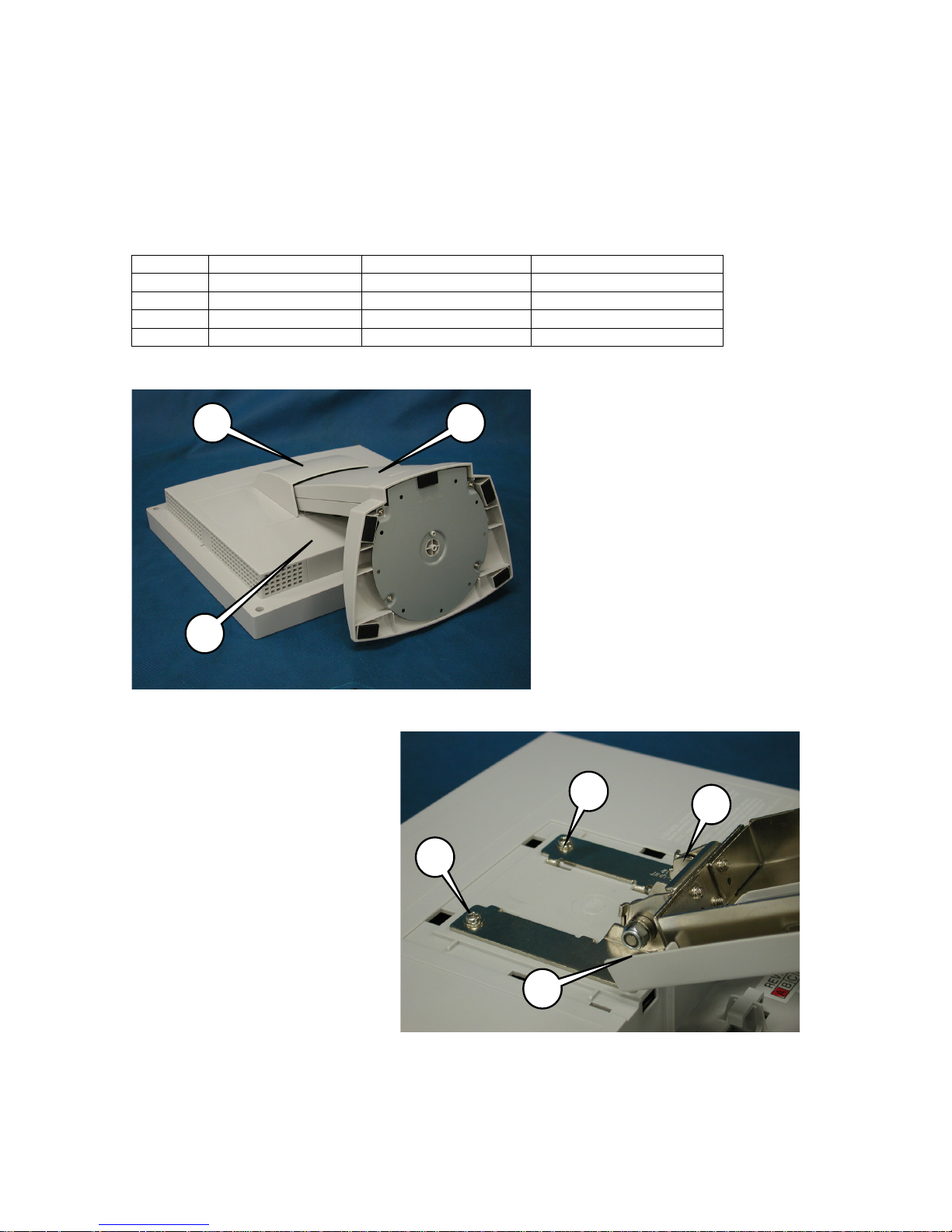
SYMBOL Part No. for NPG Part No. for NMV DESCRIPTION
1 11000842 79PQ5007 COVER, TILT, REAR
2 11000831 79PQ5006 COVER, HINGE
3 11000791 79PQ5003 COVER, CABLE
4
14300171 ---
P4*12/W MC(NI)
12
3
4
4
4
4
Page 22
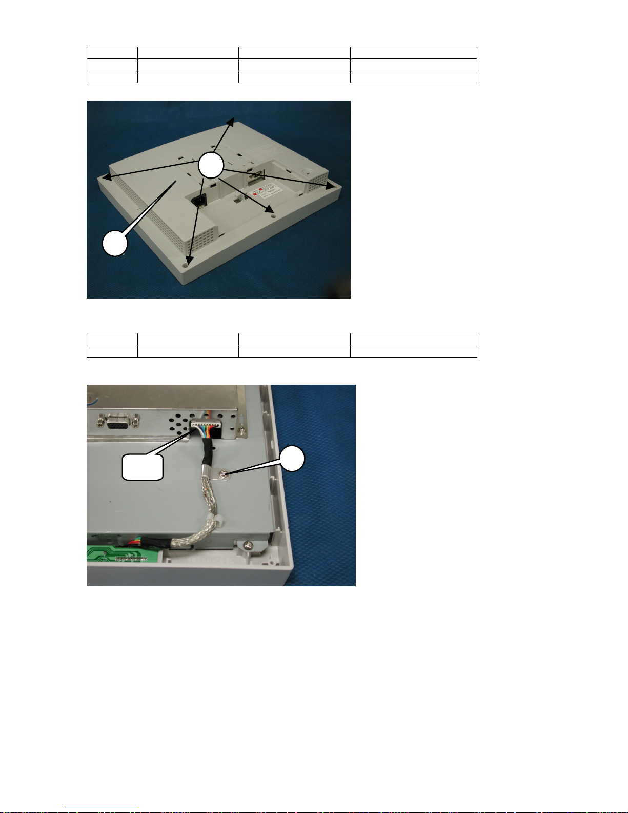
3-2
SYMBOL Part No. for NPG Part No. for NMV DESCRIPTION
5 10102971 79PQ5001 CABINET BACK
6 14000181 --- SCREW T3X10
SYMBOL Part No. for NPG Part No. for NMV DESCRIPTION
7 14300071 --- P3*6/W MC (NI)
5
6
7
J102
Page 23
3-3
SYMBOL Part No. for NPG Part No. for NMV DESCRIPTION
7 14300071 --- P3*6/W MC (NI)
8 14000171 --- VB-1 4*10 MC(NI)
9 10102981 79PQ5002 CABINET FRONT ASSY
10 AS0R21ML 79PQ5068 SW INSERT ASSY
SYMBOL Part No. for NPG Part No. for NMV DESCRIPTION
7 14300071 --- P3*6/W MC (NI)
11 12300831 --- SHIELD, COVER
12 14300201 --- 4#-40T*40T*4.8HL*4.0*5-NI/W
11
7
8
9
10
7
12
Page 24

3-4
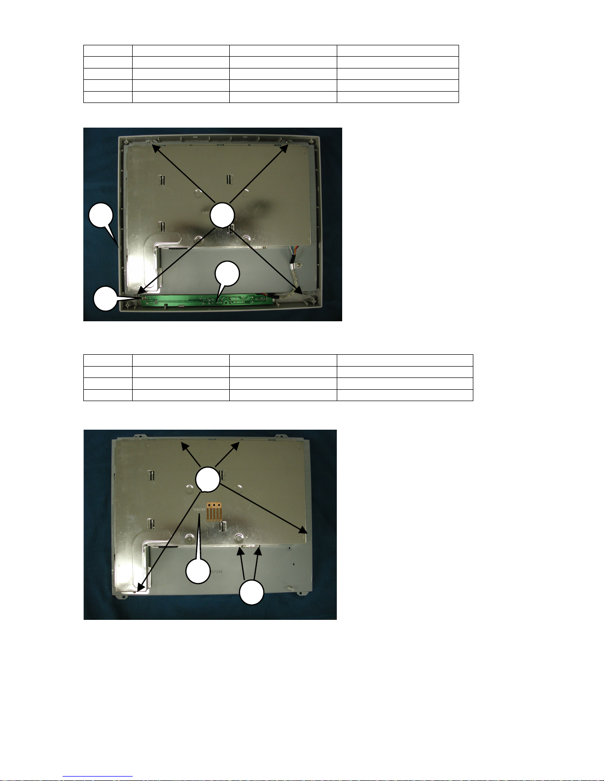
SYMBOL Part No. for NPG Part No. for NMV DESCRIPTION
13 14300161 --- P3*8*8+SPW+WAS MC(NI)
14 AM0R22ML 79PQ5011 MAIN INSERT ASSY
SYMBOL Part No. for NPG Part No. for NMV DESCRIPTION
13 14300161 --- P3*8*8+SPW+WAS MC(NI)
15 14300181 --- P3*8*8+SPW+GEAR MC(NI)
16 14300091 --- F3*8 MC (NI)
17 14300151 --- P4*10*10+SPW+WAS MC(NI)
18 AP0R22ML 79PQ5067 POWER INSERT ASSY
19 JM100011 --- INVERTER TAD770 TDK
14
13
J302
J301
J601
15
19
CN3
CN2
CN1
17
16
13
18
Page 25

3-5
SYMBOL Part No. for NPG Part No. for NMV DESCRIPTION
20 14300211 --- P2.5*4 MC (NI)
SYMBOL Part No. for NPG Part No. for NMV DESCRIPTION
21 JG552011 79PQ5063 TFT LM150X05-A3 LGPL
22 AK0R21TL 79PQ5069 CN SMT8S9 ASSY
20
21
22
Page 26

3-6
SYMBOL Part No. for NPG Part No. for NMV DESCRIPTION
8 14000171 --- VB-1 4*10 MC(NI)
17 14300151 --- P4*10*10+SPW+WAS MC(NI)
23 11000811 79PQ5004 COVER, TILT, FRONT
24 14900012 79EN0287 HINGE UNIT
25 12000621 79EN0282 TILT, FRAME, STAND
26 11000821 79PQ5005 TILT, BASE
SYMBOL Part No. for NPG Part No. for NMV DESCRIPTION
6 14000181 --- SCREW T3X10
8 14000171 --- VB-1 4*10 MC(NI)
27 12300681 79EN0528 SHIELD, BASE
23
26
8
6
9
27
24
25
17
Page 27

4-1
ADJUSTMENT PROCEDURES
TABLE OF CONTENS
Page
1. Application --------------------------------------------------------------------------------------------------- 4-2
2. Standard setting states ----------------------------------------------------------------------------------- 4-2
3. Names of each LCD monitor part, and adjustment method ------------------------------------- 4-2
3.1. Configuration of front control panel -------------------------------------------------------------------- 4-2
3.2. OSD operation method ----------------------------------------------------------------------------------- 4-2
4. Set adjustments -------------------------------------------------------------------------------------------- 4-3
4.1. Measuring instruments to be used --------------------------------------------------------------------- 4-3
4.2. Power source voltage ------------------------------------------------------------------------------------- 4-3
4.3. Electrification ------------------------------------------------------------------------------------------------ 4-3
4.4. BIAS and GAIN adjustment ----------------------------------------------------------------------------- 4-3
4.5. Panel BRIGHTNESS check ----------------------------------------------------------------------------- 4-3
4.6. Panel color check ------------------------------------------------------------------------------------------ 4-3
4.7. Color temperature check --------------------------------------------------------------------------------- 4-4
Page 28

4-2
1. Application
This adjustment procedure applies to the 15-inch LCD display (E55LCD).
2. Standard setting state
Unless designated in particular, the test is carried out with the following state.
Item State for Adjustment
Power voltage AC100V ~ 240V
Input frequency 1024 X 768 ;75Hz
Input connector D-SUB
BRIGHTNESS 100%
CONTRAST 80%
SHARPNESS 0
Color Temperature 6500K
OSD time off 30 seconds
Language English
OSD transparency 100%
OSD
setting
Power saving Yes
3. Names of each LCD monitor part, and adjustment method
3.1 Configuration of front control panel
3.2 OSD operation method
<Factory mode>
-Hot key for reset EEPROM data-
Press (▲) and (▼) button at the same time then power on.
-Hot key for Factory adjust-
Press MENU (
), and SELECT( ) button at the same time then power on.
-How to return to User mode-
To return to User mode, turn POWER-SW OFF.
Page 29

4-3
4.Set adjustments
4.1 Measuring instruments to be used
The measuring instruments considered necessary for the adjustment of the E55LCD set are specified below.
(1) Equipment that can generate an output of the adjusted VG-819 unit or equivalent.
4.2 Power source voltage
100 - 120V/ 220 - 240V±5%, 50/60Hz
4.3 Electrification
(1) Make connections according to the mode intended for VG-819 cable setting.
(2) Turn on the power switch of the VG-819 unit.
(3) Connect an AC power cable to the unit under inspection.
(4) The LED of the unit under inspection is lit in amber.(In the middle of signal discrimination)
(5) After the completion of signal discrimination, the LED is lit in green.
4.4 BIAS and GAIN adjustment
(1) Input timing 1024X768;75Hz, XGA75 with signal generator, then set the pattern to 32gray scale
and video signal level to 0.7V.
(2) OSD select to WHITE BALANCE then press (▲) or (▼) button.
(3) Automatic adjustment of BIAS and GAIN.
4.5 Panel BRIGHTNESS check
(1) Input timing 1024X768;75Hz, XGA75 with signal generator, then set pattern to full white and video signal
level to 0.7V.
(2) OSD setting BRIGHTNESS and CONTRASST to max(100).
(3) Color temperature setting to user.
(4) Check the center luminance should >= 170 cd/m2.
4.6 Panel color check
(1) Input timing 1024X768;75Hz, XGA75 with signal generator, then set pattern to full white and video signal
level to 0.7V.
(2) Color temperature setting to user.
(3) Check the center color coordination.
x = 0.313+/- 0.03 y = 0.329 +/- 0.03
Page 30

4-4
4.7 Color temperature check
(1) Input timing 1024X768;75Hz, XGA75 with signal generator, then set pattern to full white and video signal
level to 0.7V.
(2) OSD brightness setting to MAX(100) and contrast setting to 80.
(3) OSD into factory mode and adjust R;G;B gain to meeting below color coordination.
(4) Each color temperature setting as below
9300K: x = 0.281+/- 0.03 y = 0.311 +/- 0.03
8200K: x = 0.290+/- 0.03 y = 0.300 +/- 0.03
7500K: x = 0.300+/- 0.03 y = 0.310 +/- 0.03
6500K: x = 0.313+/- 0.03 y = 0.329 +/- 0.03
5000K: x = 0.345+/- 0.03 y = 0.352 +/- 0.03
Page 31

5-1
INSPECTION
TABLE OF CONTENS
Page
1. Electric performance ------------------------------------------------------------------------------------- 5-2
1.1. Confirming the operation of operation SW --------------------------------------------------------- 5-2
1.2. Frequency change speed ------------------------------------------------------------------------------- 5-2
1.3. Confirming power management function ----------------------------------------------------------- 5-2
2. Safety test -------------------------------------------------------------------------------------------------- 5-2
2.1. Isolation voltage ------------------------------------------------------------------------------------------- 5-2
2.2. Ground resistance ---------------------------------------------------------------------------------------- 5-2
3. Factory mode ---------------------------------------------------------------------------------------------- 5-3
4. External inspection on the LCD module ------------------------------------------------------------- 5-5
5. Inspection of PLUG & PLAY Communication and OSD "MONITOR INFORMATION" for
Model Name/ Serial Number -------------------------------------------------------------------------- 5-8
5.1. System Connection -------------------------------------------------------------------------------------- 5-8
5.2. Input Signal ------------------------------------------------------------------------------------------------ 5-8
5.3. Programs Required -------------------------------------------------------------------------------------- 5-8
5.4. Inspection Procedures ---------------------------------------------------------------------------------- 5-8
5.5. Error Messages ------------------------------------------------------------------------------------------- 5-11
5.6. EDID Data File --------------------------------------------------------------------------------------------5-11
6. Preset Timing ---------------------------------------------------------------------------------------------- 5-12
Page 32

5-2
1. Electric performance
1.1 Confirming the operation of operation SW
(1) Input XGA75 pattern “Crosshatch”.
(2) The picture must appear within four seconds after turning power switch ON.
(3) Confirm that Power-On Indicator is lit.
(4) Synchronization must not flow when power switch is turned ON and OFF.
(5) OSD must appear when Menu or Select button is pressed.
(6) The setting value must smoothly change and abnormalities such as noise must not occur when (▲) / (▼)
button is pressed.
(7) Press OSD OFF button, and confirm that OSD picture disappears.
1.2 Frequency change speed
(1) Change the preset timing.
(2) Confirm that it does not take so long time to change the picture when frequency is changed. (Within five
seconds)
1.3 Confirming power management function
(1) Input the specified timing with signal generator, and set the pattern to full white.
Mode H V Power voltage Input timing Power consumption
Normal On On AC240V XGA75 25W
Standby Off On AC240V XGA75 3W
Suspend On Off AC240V XGA75 3W
Off Off Off AC240V XGA75 3W
2 Safety test
2.1 Isolation voltage
Confirm that the abnormality is never seen when AC1500V is applied for two seconds across AC earth GND
pin to chassis GND. Cut-off current must be 10mA.
2.2 Ground resistance
Confirm that the resistance must be less than 100m ohms or less when 25A is applied across AC earth GND
pin to chassis GND.
Page 33

5-3
3. Factory mode
Mention the contents of the factory menu letter.
Page 1:
1. A “Menu” key is pressed and the "BIAS" menu is displayed.
2. Press
”Select” key to adjust the cursor to R,G or B.
3. Press (▲) or (▼) key can adjust each value is changed.
Page 2:
1. A
“Menu” key is pressed and the "GAIN" menu is displayed.
2. Press
”Select” key to adjust the cursor to R,G or B.
3. Press (▲) or (▼) key can adjust each value is changed.
Page 3:
1. A “Menu” key is pressed and the "SERVICE INFORMATION" menu is displayed.
2. The page can check "TOTAL TIME", "ON TIME" and firmware version.
Page 4:
1. A “Menu” key is pressed and the "ON TIME RESET" menu is displayed.
2. Reset by (▲) or (▼) key.
Page 34

5-4
Page 5:
1. A
“Menu” key is pressed and the "TOTAL TIME RESET" menu is displayed.
2. Reset by (▲) or (▼) key.
Page 6:
1. A
“Menu” key is pressed and the "EEP WRITE PROTECT" menu is displayed.
2. Change setting EEPROM write Protect by
”Select” key.
YES: Disable
NO : Enable
Page 7:
1. A
“Menu” key is pressed and the "ALL RESET" menu is displayed.
2. Reset all EEPROM date and load default value to EEPROM by (▲) or (▼) key.
Page 8:
1. A
“Menu” key is pressed and the "COLOR TEMPERATURE" menu is displayed.
2. Select R,G,B by
”Select” key.
3. Press (▲) or (▼) key can adjust each value is changed.
Left side : Red
Center : green
Right side : Blue
Page 35

5-5
4. External inspection on the LCD module
RG GB RG GB
RG RG RG RG RG RG
etc.
: Bright Do
t
: Dark Do
t
Note 1. Horizontally adjacent 2 dots (R+G, G+B)
Note 2. 1) + 2) : Max. 3
Combination
with Bright
&Dark Dot
Combination except horizontally
adjacent 2 dots.
Count as horizontally adjacent 2 dots
Do not count as adjacent 2 dots
Items Criteria Remarks
1
)
Bright Dots Horizontally adjacent 2 dots (R+G, G+B
)
Max. 2 Note 1
2
)
Dark Dots Horizontally adjacent 2 dots (R+G, G+B
)
Max. 2 Note 2
3) Bright Dots
Horizontally, vertically or combined adjacent 3 dots (separately
bri
g
ht dots and dark dots
)
Not
Allowed
4) Dark Dots
Not
Allowed
Dot Defect 5)
Dot defect except
1
), 2)
R or G or B (Bright Dot + Dark Dot) Max. 6 Note 4
6)
Distance between
bri
g
ht dots
Distance between bright dots (R - R): less than 6.5mm
Max. 2 for
each color
Note 5
7)
Distance between
6
)
's
Distance between 6)s : less than 15mm
Not
Allowed
Note 6
Two or more
p
ixels or sub-pixels with more than one fault of 5)Max. 3 Note 7
Two or more
p
ixels or sub-pixels with more than one fault of 1
)
Two or more pixels or sub-pixels with more than one fault of 2
)
Max. 10 -
Max. 6 -
Total amount of Bright Dot (G)
Note 9. Every dot herein means sub-pixel (each Red, Green or Blue color)
Note 10. Bright & Dark Dots are larger than one third of sub-pixel. (Dots smaller than one third of sub-pixel are not counted as a defect
dots.
)
Note 11. Do not use the [ND] filter in counting a bright dot.
Total amount of Dot
Defects
Total amount of Bright Dot (R,G,B) and Dark Dot (R,G,B)
Adjacent Dots
Note 3
Fault cluster
Not
Allowed
Note 8
8)
Min. Distance between
bright dots
Page 36

5-6
Note 3. Horizontally, vertically or combined adjacent 3 dots (separately bright dots and dark dots)
Note 4. Do not count the horizontally adjacent 2 dots (R-G, G-B)
Note 5. Distance between bright dots
Note 6. Distance between the group of 6)'s.
Count as adjacent 3 dots
Do not count as adjacent 3 dots
RRGGBBRRGGBBRGGBBR
Distance between the same color
Combination with Bright Dot & Dark
Dot
≤ 6.5mm ≤ 6.5mm ≤ 6.5mm ≤ 6.5mm ≤ 6.5mm ≤ 6.5mm ≤ 6.5mm ≤ 6.5mm ≤ 6.5mm
Count as defect Do not count as defect
RR RR GG GG B B BB
≤ 6.5mm ≤ 6.5mm
≤ 6.5mm
≤ 6.5mm ≤ 6.5mm ≤ 6.5mm
≤15mm ≤15mm ≤15mm
Count as defect
Combination with the different color
Page 37

5-7
Note 7. Two or more pixels or sub-pixels with more than one fault of 5) within 5x5 pixels
Note 8. Two or more pixels or sub-pixels with more than one fault of 1) or 2) within 5x5 pixels
5x5 pixels
1 Cluster
The number of cluster within all screen : Max. 3
RG RG RG
RG RG RG
5x5 pixels
5x5 pixels 5x5 pixels
Count as defect
Do not count as defect
Page 38

5-8
5. Inspection of PLUG & PLAY Communication and OSD "MONITOR INFORMATION"
for Model Name/ Serial Number
5.1 System Connection
This system should be connected as shown below.
EDID JIG
(NPG)
Signal Cable
Signal Cable
Printer Cable
Signal Generator
DESKTOP/NOTE
PC
Monitor
Program Disk
Part No.599910508
Part No. 599910593
EDID JIG (NPG)
5.2 Input Signal
Horizontal sync frequency: Not specified.
Vertical sync frequency: Not specified.
5.3 Programs Required
NPGV233.EXE
E55LCD.BAT
E55LCD.TXT
5.4 Inspection Procedures
a. Factory Mode: Press “Menu“ and ”Select” button at the same time then power ON.
b. A
“Menu” button is pressed and the "EEP WRITE PROTECT" menu is displayed.
Page 39

5-9
c. A
”selection” button is pressed and cursor is moved to "NO."
d. Copy the above-mentioned programs in an adequate directory.
e. Set up the MO-DOS mode. (DOS Prompt of Windows95/98 is also acceptable.)
f. Execute the E55LCD.BAT from the command line.
g. Press the F2 key to start the inspection of DDC2B.
As a result of inspection, when EDID data is not written in or it differs, h or later is performed.
h. Check the serial number of the set and enter an input of the following code from the keyboard.
08R220B3 Serial Number (Model Code + 1 Space + Serial No.)
Example: 08R220B3 2600001YB
Page 40

5-10
i. Press the Enter key. Then, the EDID data, OSD model name, and the serial number begin to be
written in.
j. Display “MONITOR INFO.” of the OSD, and confirm that the model name and serial number have been
correctly written.
k. Press the F2 key to start the inspection of DDC2B.
After the completion of inspection, the contents of EDID are displayed. If an error should occur, the
related error message will be displayed in the bottom area of the screen. Refer to Paragraph 7.5 in
regard to the meaning of this error message.
Page 41

5-11
5.5 Error Messages
• IIC Communication Error
Communication disabled
• EDID Check Sum Error
Entry of false EDID
• DDC2 Does Not Find Head Data
DDC2 Communication disabled
5.6 EDID Data File
The EDID data file text is shown below. When you write or inspect EDID for this monitor, the following table
can be used.
File name : E55LCD.TXT
0123456789ABCDEF
00
00 FF FF FF FF FF FF 00 34 AC 4E 46 01 01 01 01
10
1A*10C*201 03 08 1E 17 78 EA 7E A5 A0 58 4E 96 25
20
1E 50 54 BF EE 00 01 01 01 01 01 01 01 01 01 01
30
01 01 01 01 01 01 C3 1E 00 20 41 00 20 30 10 60
40
13 00 30 E4 10 00 00 1E 00 00 00 FD 00 37 4B 1F
50
3C 08 00 0A 20 20 20 20 20 20 00 00 00 FC 00 45
60
35 35 4C 43 44 0A 20 20 20 20 20 20 00 00 00 FF
70
00 31*335*330*330*330*330*331*349*341*30A*320*320*320*300 8D
*4
Table 7.6 Data list
*1 : address 10h Manufactured month x 4
*2 : address 11h Manufactured year - 1990
*3 : address 71h ~ 7Dh Input serial number (ASCII code)
Add 0Ah after serial number.
Add 20th remaining address.
*4 : address 7Fh Checksum. The sum of entire 128byte shall be equal to 00h.
Page 42

5-12
6. Preset Timing
Horizontal Vertical
NO
Timi ng
name
Dot
Clock
(MHz)
f
requency
Fh
(KHz)
Period
Th
(µS)
SYNC.
pulse
Ths
(µS)
Front
porch
Thf
(µS)
Back
porch
Thb
(µS)
Display
time
Thd
(µS)
frequency
FV
(Hz)
Period
Tv
(ms)
SYNC.
pulse
Tvs
(ms)
Front
porch
Tvf
(ms)
Back
porch
Tvb
(ms)
Display
time
Tvd
(ms)
HS/VS
Polarity
1
MAC13 30.24
35.00
(Dots)
28.57
864
2.12642.12643.179621.16
640
66.67
(Lines)
15.00
525
0.0930.0931.113913.71
480
N,N
2
MAC16 57.24
49.70
(Dots)
20.13
1152
1.12640.56323.91
224
14.54
832
74.52
(Lines)
13.42
667
0.0630.0210.783912.56
624
N,N
3
VGA350 25.175
31.47
(Dots)
31.78
800
3.81960.64161.914825.42
640
70.08
(Lines)
14.27
449
0.0621.18371.916011. 12
350
P,N
4
VGA60 25.175
31.47
(Dots)
31.78
800
3.81960.64161.914825.42
640
59.94
(Lines)
16.68
525
0.0620.32101.053315.25
480
N,N
5
VGA75 31.50
37.50
(Dots)
26.67
840
2.03640.51163.81
120
20.32
640
75.00
(Lines)
13.33
500
0.0830.0310.431612.80
480
N,N
6
VESA720 28.32
31.47
(Dots)
31.78
900
3.81
108
0.64181.915425.42
720
70.08
(Lines)
14.27
449
0.0620.41131.083412.71
400
N,P
7
SVGA56 36.00
35.16
(Dots)
28.44
1024
2.00720.67243.56
128
22.22
800
56.25
(Lines)
17.78
625
0.0620.0310.632217.07
600
P,P
8
SVGA60 40.00
37.88
(Dots)
26.40
1056
3.20
128
1.00402.208820.00
800
60.32
(Lines)
16.58
628
0.1140.0310.612315.84
600
P,P
9
SVGA72 50.00
48.08
(Dots)
20.80
1040
2.40
120
1.12561.286416.00
800
72.19
(Lines)
13.85
666
0.1260.77370.482312.48
600
P,P
10
SVGA75 49.50
46.88
(Dots)
21.33
1056
1.62800.32163.23
160
16.16
800
75.00
(Lines)
13.33
625
0.0630.0210.452112.80
600
P,P
11
XGA60 65.00
48.36
(Dots)
20.68
1344
2.09
136
0.37242.46
160
15.75
1024
60.00
(Lines)
16.67
806
0.1260.0630.602915.88
768
N,N
12
XGA70 75.00
56.48
(Dots)
17.71
1328
1.81
136
0.32241.92
144
13.65
1024
70.07
(Lines)
14.27
806
0.1160.0530.512913.60
768
N,N
13
XGA72 78.08
58.10
(Dots)
17.21
1344
1.72
134
0.33262.05
160
13.11
1024
72.08
(Lines)
13.87
806
0.1060.0530.502913.22
768
N,N
14
XGA75 78.75
60.02
(Dots)
16.66
1312
1.22960.20162.23
176
13.00
1024
75.03
(Lines)
13.33
800
0.0530.0210.472812.80
768
P,P
15
XGA60 65.00
48.36
(Dots)
20.68
1344
2.09
136
0.37242.46
160
15.75
1024
60.00
(Lines)
16.67
806
0.1260.0630.602915.88
768
P,P
16
VGA73 31.5
37.86
(Dots)
26.41
832
1.27400.76244.06
128
20.32
640
72.81
(Lines)
13.73
520
0.0830.2490.742812.68
480
N,N
17
SUN 70.49 52.45
19.04
1344
1.93
136
0.34241.27
160
14.53
1024
65.07
15.37
806
0.1160.0630.552914.64
768
P,N
18
PAL 27 31.25
32
864
3.59971.74470.71925.95
700
50
20
625
0.39312
1.13350.072218.4
575
N,N
Page 43

6-1
TROUBLE SHOOTING
TABLE OF CONTENTS
Page
1. No display of screen (Screen is black, color of LED is amber) ---------------------------------- 6-2
2. Nothing displays on screen (Screen is black, color of LED is green) -------------------------- 6-3
3. Checking the back light unit ----------------------------------------------------------------------------- 6-6
4. Abnormal screen ------------------------------------------------------------------------------------------- 6-7
5. Abnormal plug and play operation --------------------------------------------------------------------- 6-8
5.1 Abnormal DDC2 ------------------------------------------------------------------------------------------- 6-8
6. Checking the interface circuit of sync signal --------------------------------------------------------- 6-9
6.1 Checking the control circuit of horizontal sync pulse --------------------------------------------- 6- 9
6.2 Checking the control circuit of vertical sync pulse ----------------------------------------------- 6-10
7. Checking the resolution change IC movement ----------------------------------------------------- 6-11
8. No power on ------------------------------------------------------------------------------------------------ 6-12
9. Checking the operation of CPU ------------------------------------------------------------------------ 6-13
Page 44
6-2
1. No display of screen (Screen is black, color of LED is amber)
When a signal isn't being inputted, it is indicated with "NO SIGNAL".
It is indicated with "OUT OF RANGE" at the time of the frequency
that it over spec.timing.
NO
Y
ES
NG
OK
Does OSM display when you
push “Menu, Select ,UP or
DOWN” button.
Proceed section 2 “Nothing
display on screen”
Check if the sync signal from Computer is output
and if the video cable is connected normally.
Input the sync signal of computer,
or change the cable.
Proceed section 7 “Checking the resolution
change IC movement”.
Page 45

6-3
2. Nothing displays on screen (Screen is black, color of LED is green)
NG
OK
NG
OK
OK
NG
NG
OK
Is backlight lit?
Refer to section 3 “Checking the backlight unit.
Does computer output RGB
video signals?
1) Change pattern of video signal output on the host.
2) Reconnect the video cable.
3) Change the video cable.
Check OSM menu is
displayed on screen when
you push the
“Menu,Select,Up or Down”
key.
Check if the LCD video signal cable is connected
between the MAIN board and LCD module.
Failure point
The cable is disconnected.
Next page
Proceed section 4 “Abnormal
screen “.
Check the video cable for failure.
Check the host for output signal with all black only.
Page 46

6-4
OK
OK
OK
OK
NG
NG
NG
NG
NG
Continue
Is 5V voltage provided to pins 38 and 39 of J301
in MAIN board?
Is 5V voltage provided to
pin 38 and 39 of J301.
OK
Failure point
Is a PCLK being outputted under the condition
that pin2 of J301in main BD?
Failure point
Check the DE pulse is output on J301 pin4?
Check the PVD signal is ouput on J301 pin5 .
J301 cable pulled out or
disconnected.
1) IC401 failure.
2) Printed wire broke between
IC401 and J301pin2.
3) R436;C343or R306 failure.
Failure point
1) U3 failure.
2) Printed wire broke between
IC401 and J301 pin4.
3) R439 or C344 failure.
Failure point
1) U3 failure.
2) Printed wire broke between
IC401 and J301 pin5.
3) R438, C345 failure.
next page
Failure point
Check Q301and IC301.
Page 47

6-5
Continue
Check the PHD signal is ouput on J301 pin6.
OK
NG
Failure point
1) IC401 failure.
2) Printed wire broke between
U401 and J301 pin6.
3) R437 or C346 failure.
Check the data signal output on J301 and J302
R, G, B data pin.
OK
NG
Failure point
1) IC401 failure.
2) Printed wire broke between
IC401 data line and J301,
J302.
Failure point
1) The cable broke between J301, J302 and
Panel connect Board.
2) Connect Board fail.
3) LCD module failure .
Page 48

6-6
3. Checking the back light unit
NG
NG
OK
NG
OK
Is 12V voltage provided to
inverter?
Failure point
Check the ON/FF signal
of equal “H” at CN1 pin6?
Check Inverter F1 open.
Failure point
F1 failure. Replace the
inverter board.
Failure point
1) Inverter cable disconnection.
OK
1) µ-p failure.
2) Printed wire broke
between µ-p trace to CN1
pin6.
Is 12V-source voltage
provided to pins 1 and 2 of
CN1 in inverter module?
OK
NG
Failure point
Inverter cable disconnection.
Check Power Board.
Page 49

6-7
4. Abnormal screen
NG
NG
OK
OK
Check the R, G, B video signal from computer
input on D-Sub R,G,B connector.
Failure point
1) No R, G and B video signal output from host
computer. Check computer.
2) Video signal cable disconnection.
Check the R,B,G input signals on IC401 pin 2,
13, 20,respectively that their level is 0.7Vp-p
typical.
Failure point
In the case of the Red signal.(A Green and
Blue signal is the same path, too.)
Printed wire broke between D-Sub(R,G,B) and
IC401 pin 2,13,20.
Is the pulse of the TTL level being out put to
J301 and J302 from the data line of IC401?
Proceed section 7 “Checking the resolution change IC
movement”.
NG
OK
Failure point
Printed wire broke between IC401 data line
and J301,J302.
Check the PHD sync pulse output to J301 pin6
from IC401 pin53 at TTL level.
Failure point
Printed wire broke between IC401 pin53 and
J301 pin6.
NG
OK
Check the PVD sync pulse output to J301 pin5
from IC401 pin54 at TTL level.
Failure point
Printed wire broke between IC401 pin54 and
J301pin5.
NG
OK
Check the PDE sync pulse output to J301 pin4,
from IC401 pin126 at TTL level.
Failure point
Printed wire broke between IC401 pin126 and
J301 pin4.
OK
NG
Page 50

6-8
5. Abnormal plug and play operation
Abnormal DDC2B
Confirm the output of serial data on IC201 pin 6
synchronize SCLK at TTL level.
NG
Failure point
IC201 failure.
Failure point
1) The host machine isn't communicating in DDC2B mode.
2) The video cable may have failed or may not to have
connections for DDC.
3) Between IC201 pin 6 and J201 pin 15 may have failed.
4) Cable failure.
OK
Page 51

6-9
Check the hovizuntal sync signal on IC401 pin141
a TTL level.
6. Checking the interface circuit of sync signal
6.1 Checking the control circuit of horizontal sync pulse
Check the horizontal sync signal on IC202 pin1 at
TTL level.
NG
OK
Failure point
1) No separate sync or composite sync
output by host. (Confirm the host,
output the sync signal.)
2) Video cable may have failed.
3) Printed wire broke between J201
pin 13 and IC202 pin1.
4) L208 or R213 open.
5) IC202 failure.
Procees section 7 “Checking the resolution change
IC movement”.
NG
OK
Failure point
IC401 failure.
Page 52

6-10
6.2 Checking the control circuit of vertical sync pulse
Check the vertical sync signal on IC202
pin5 at TTL level.
NG
Failure point
1)No separate sync output signal from the host.(Chec
k
the host.)
2) Video cable may have failed.
3) Printed wire broke between J201 pin 14 and IC202
pin5
4) L208 or R215 open.
5) IC202 failure.
OK
Proceed section 7 “Checking the resolution
change IC movement”.
Page 53

6-11
7. Checking the resolution change IC movement
Is there +3.3V supply on IC401 pins49, 57, 67, 79, 89, 101, 113, 125, 132, 143, 159. Is there
+2.5V SUPPLY ON IC401 PIN 3, 6,14,17, 21,24, 26, 32, 38, 46, 71, 91, 103,123, 145,147,
152;Is there +3.0V supply on IC401 Pin8.
NG
OK
Is 25MHz clock input to IC401 pin47 at TTL
level?
NG
OK
OK
Proceed section 11 "Checking the
DC/DC converter circuit".
Is 25MHz clock output from X401 at TTL
level?
Failure point
X401 failure
Proceed section 7 “Checking the resolution
change IC movement”.
Page 54

6-12
8. No power on
Check the +12V power provided from Power
Board.
NG
OK
Failure point
Power Board failure.
Check the +5V and +3.3V power from IC601.
NG
OK
Failure point
"Checking the DC/DC
converter circuit".
Proceed section 9 "Checking the operation of
CPU ".
Page 55

6-13
9. Checking the operation of CPU
Is there +3.3V supply on IC102 pins44?
NG
OK
Failure point
L110 open.
Is 12MHz clock input to IC102 pin20, 21 a
t
TTL level?
NG
OK
Failure point
X101 failure.
Failure point
IC102 failure.
Page 56

7-1
CIRCUIT DESCRIPTION
TABLE OF CONTENTS
Page
1. Power circuit ------------------------------------------------------------------------------------------------- 7-2
1.1 Power input ------------------------------------------------------------------------------------------------- 7-2
1.2 Soft-power circuit ------------------------------------------------------------------------------------------ 7-2
1.3 DC to Dc circuit -------------------------------------------------------------------------------------------- 7-2
1.4 Panel Vcc control ------------------------------------------------------------------------------------------ 7-2
2. Microprocessor control circuit ---------------------------------------------------------------------------- 7-2
2.1 Clock circuit ------------------------------------------------------------------------------------------------- 7-2
2.2 I2C buses --------------------------------------------------------------------------------------------------- 7-2
2.3 General-purpose port ------------------------------------------------------------------------------------ 7-2
2.3.1 Key scan status ----------------------------------------------------------------------------------------- 7-2
2.3.2 Scaler control -------------------------------------------------------------------------------------------- 7-2
2.3.3 Led control ----------------------------------------------------------------------------------------------- 7-3
2.3.4 Data memory -------------------------------------------------------------------------------------------- 7-3
3. Scaler ---------------------------------------------------------------------------------------------------------- 7-3
Page 57

7-2
1 Power Circuit
1.1 Power input
12V DC input from power Board through J601 to interface.
1.2 Soft-power circuit
IC602 control the Q602 and Q601 for 12V into the DC to DC circuit .
IC602 pin5 Low is OFF status ; Hi is ON status
While “ON” status DC to DC circuit output 5V and 3.3V
While “OFF” status DC to DC circuit is not activity.
1.3 DC to DC circuit
IC610 is used generate the system power. It have built in 2 channel PWM controller to provide two voltage
output.
One (5V) is provide panel Vcc and 2.5V regulator input.
The other (3.3V) is provide the Scaler and MCU power.
1.4 Panel Vcc control
Panel power control used Q301 and IC301 from IC102 (pin19) PANELVCC_CTL.
While the PANELVCC_CTL stay at High level ;the panel voltage is 5V.
While the PANELVCC_CTL stay at Low level ;the panel voltage is 0V.
2 Microprocessor Control circuit
2.1 clock circuit
The X101 is crystal ;it generates an 12M Hz output for microprocessor.
2.2 I2C buses
IC102 (pin 40) SDA Serial data
IC102 (pin 39) SCL Serial clock
This is I2C serial communication bus and is used for READ or WRITE data communication of IC101 and
IC401.
2.3 General-purpose port
2.3.1 Key scan status
IC102 pin2 is for OSD “Menu” adjust
IC102 pin3 is for OSD “Select” adjust
IC102 pin4 is for OSD “Up” adjust
IC102 pin5 is for OSD “Down” adjust
2
.3.2 Scaler control
IC102 pin14 (I/O) for scaler interrupt signal
IC102 pin 30 output scaler reset signal
Page 58

7-3
2.3.3 LED control
IC102 pin 42 control Q102 for Green LED lit.
IC102 pin 43 control Q101 for RED LED lit.
2.3.4 Data memory
The display control data are held by the EEPROM(IC101); These display control data are accessed
through the I2C bus of the MCU.,
3 Scaler
The scaler IC (IC401) is controlled by MCU through the I2C bus.
IC401 embeded the ADC provide with the analog interface input.
X401 output 25M Hz fed to IC401.
IC202 schmitt trigger for sync.waveform processor. And fed to IC401 for mode detect.
Page 59

REPLACEMENT PARTS LIST
The components specified for Model E55LCD
SYMBOL
Part No for NPG
Part No for NMV DESCRIPTION
*** ICS ***
IC101 EHA10081 79PQ5015 IC SMD 24LC16B SO8
IC102 EHA10251 79PQ5019 IC NT68F631L MCU8BIT128K
IC201 EHA10091 79PQ5016 IC SMD 24LC21 SO8
IC202 EH160011 79EN0550 IC FTTL 74F14SJ SO
IC401 EHA10061 79PQ5013 IC SMD SAA6713AH SCALER
IC402 EHA10071 79PQ5014 IC SMD PJ1117CW-2.5V REGU
IC601 EHA10111 79PQ5018 IC SMD MB3775PF-ER A/D
IC602 EHA10101 79PQ5017 IC SMD 74F74 SO14
IC901 EH170021 79PQ5012 IC TOP245Y HYBRID POWER
IC902 EH190021 79EN0553 IC PHOTO COUPLE PC123Y
IC921 EH190011 79EN0552 IC KIA431A-AT
*** TRANSISTORS ***
IC301 EQ500117 79EN0587 FET CHIP HAT1053M
Q101 EP000313 79EN0583 TR CHIP 2SA1037AK-T146R
Q102 EP000313 79EN0583 TR CHIP 2SA1037AK-T146R
Q103 EN000211 79EN0576 TR CHIP NPN DTC114EUA
Q201 EN000211 79EN0576 TR CHIP NPN DTC114EUA
Q301 EN000211 79EN0576 TR CHIP NPN DTC114EUA
Q601 EP000611 79PQ5025 TR 2SB1424 SOT89
Q602 EN000211 79EN0576 TR CHIP NPN DTC114EUA
Q603 EQ500411 79PQ5076 FET SMD P SI230IDS-TI
Q604 EP000611 79PQ5025 TR 2SB1424 SOT89
Q605 EN000211 79EN0576 TR CHIP NPN DTC114EUA
*** DIODES ***
BD901 EJ000110 79EN0568 DIODE D2SB60A
D201 EX700216 79EN0596 DIODE RB495D
D202 EYD40562 79EN0598 ZD CHIP UDZS5.6B TE-17
D203 EX500216 79EN0594 DIODE CHIP DAN217 T146
D204 EX500216 79EN0594 DIODE CHIP DAN217 T146
D205 EX500216 79EN0594 DIODE CHIP DAN217 T146
D211 EX700115 79EN0595 DIODE CHIP CRS01 C
D401 EYE40301 79PQ5028 ZD Z02W 3.0V
D601 EX700411 79PQ5027 DIODE SSM24
D602 EX700411 79PQ5027 DIODE SSM24
D603 EYG30501 79PQ5029 ZD 5V 1/2W
D803 EL200110 79EN0573 DIODE LED SML19460C
D901 EJ300115 79EN0570 DIODE SF13
D902 EJ100041 79PQ5021 DI BYV26E 1A 1KV
D921 EJ100030 79PQ5020 DI FCQ10A06 10A 60V
8-1
Page 60

SYMBOL
Part No for NPG
Part No for NMV DESCRIPTION
PD901 EJ100061 79PQ5022 DI P6KE200A
*** TRANSFORMERS ***
T901 HE100061 79PQ5061 TRANS POWER 49A-1041
*** RELAYS & SWITCHES ***
SW800 JC300111 79EN0691 SW-TACT SKQNAED010
SW802 JC300111 79EN0691 SW-TACT SKQNAED010
SW803 JC300111 79EN0691 SW-TACT SKQNAED010
SW804 JC300111 79EN0691 SW-TACT SKQNAED010
SW805 JC300111 79EN0691 SW-TACT SKQNAED010
*** PWB ASSYS ***
MAINBD AM0R22ML 79PQ5011 MAIN INSERT ASSY
POWBD AP0R22ML 79PQ5067 POWER INSERT ASSY
SWBD AS0R21ML 79PQ5068 SW INSERT ASSY
CNBD AK0R21TL 79PQ5069 CN SMT8S9 ASSY
*** COILS & FILTERS ***
B901 HC011012 79EN0672 FERRITE WBRID-237555-H7S
B902 HC011012 79EN0672 FERRITE WBRID-237555-H7S
L102 HM011011 79EN0677 FERRITE BLM18AG121SN1
L103 HM011011 79EN0677 FERRITE BLM18AG121SN1
L104 HM011011 79EN0677 FERRITE BLM18AG121SN1
L105 HM011011 79EN0677 FERRITE BLM18AG121SN1
L106 HM011011 79EN0677 FERRITE BLM18AG121SN1
L107 HM011011 79EN0677 FERRITE BLM18AG121SN1
L108 HM011011 79EN0677 FERRITE BLM18AG121SN1
L109 HM011011 79EN0677 FERRITE BLM18AG121SN1
L110 HM012311 79EN0683 FERRITE SMB160808-N1-121P
L204 HM011011 79EN0677 FERRITE BLM18AG121SN1
L207 HM011011 79EN0677 FERRITE BLM18AG121SN1
L208 HM011532 79EN0680 FERRITE CHIP BK2125HS431
L209 HM011532 79EN0680 FERRITE CHIP BK2125HS431
L301 HM012311 79EN0683 FERRITE SMB160808-N1-121P
L302 HM012311 79EN0683 FERRITE SMB160808-N1-121P
L303 HM012311 79EN0683 FERRITE SMB160808-N1-121P
L401 HM012311 79EN0683 FERRITE SMB160808-N1-121P
L402 HM012311 79EN0683 FERRITE SMB160808-N1-121P
L403 HM012311 79EN0683 FERRITE SMB160808-N1-121P
L404 HM012311 79EN0683 FERRITE SMB160808-N1-121P
L405 HM012311 79EN0683 FERRITE SMB160808-N1-121P
L406 HM012311 79EN0683 FERRITE SMB160808-N1-121P
L407 HM012311 79EN0683 FERRITE SMB160808-N1-121P
L601 HA200051 79PQ5059 L CHOKE 33UH
L602 HA200051 79PQ5059 L CHOKE 33UH
L603 HM012311 79EN0683 FERRITE SMB160808-N1-121P
L604 HM012311 79EN0683 FERRITE SMB160808-N1-121P
8-2
Page 61

SYMBOL
Part No for NPG
Part No for NMV DESCRIPTION
L605 HM012311 79EN0683 FERRITE SMB160808-N1-121P
L606 HM012311 79EN0683 FERRITE SMB160808-N1-121P
L901 HA100101 79PQ5058 LINE FILT 30.5MH HFZ20H03
L932 HA200071 79PQ5060 L CHOKE 33UH 2A 49A-2003
L933 HA200071 79PQ5060 L CHOKE 33UH 2A 49A-2003
*** ELECTRICAL PARTS & MISCELLANEOUS PARTS ***
ACCORD RG030031 79PQ5066 PW CORD EU 2M R-PLUG GR
CABLE RE010041 79PQ5065 CABLE DSUB-DSUB GRAY 2M
F901 JA270016 79EN0689 FUSE MRT 3.15AH 250V
J402 RAJ01601 79PQ5064 CN SMD 60P SIDE
RV901 FD300018 79EN0610 VARISTOR ENE471D-10A
TFT JG552011 79PQ5063 TFT LM150X05-A3 LGPL
TH901 FD200011 79EN0609 THERMISTOR SCK103
X101 EM100031 79PQ5023 X'TAL 12M HC-49/U
X401 EM2K0021 79PQ5024 OSC SMD FN2500002 25M 50P
*** APPEARANCE PARTS ***
BASEF 17000781 79EN0290 FOOT,PAD
BASEFP 17000951 79EN0291 FOOT PAD
BASES 12300681 79EN0528 SHIELD,BASE
BASET 12000621 79EN0282 TILT,FRAME,STAND
CABB 10102971 79PQ5001 CABINET BACK
CABI B 11000831 79PQ5006 COVER, HINGE
CABIB 11000791 79PQ5003 COVER, CABLE
CABIBA 10102981 79PQ5002 CABINET FRONT ASSY
TIBA 11000821 79PQ5005 TILE, BASE
TILT 14900012 79EN0287 HINGE UNIT
TILTF 11000811 79PQ5004 COVER, TILT, FRONT
TILTR 11000842 79PQ5007 COVER, TILT, REAR
*** PRINTED & PACKING MATERIALS ***
CARTON 13202081 79PQ5008 CARTON BOX E55LCD(MITSUBI
IDLABE 15001781 79PQ5009 RATING LABEL E55 LCD (MIT
MANUAL 15501341 79PQ5010 MANUAL E55 LCD (MITSUBISH
PABAG 13700161 79EN0286 PACKING,BAG
PACKL 13400721 79EN0284 POLYLON(L)
PACKR 13400731 79EN0285 POLYLON(R)
SHEETC 15800102 79PQ5074 CAUTION SHEET
SHEETS 15900261 79PQ5075 SALES OFFICE LIST (MITSUB
*** RESISTORS ***
C626 FM010000 79EN0175 R SMD 1/10W(T) 5% 0
L201 HM015011 79PQ5079 BEAD SMD FCM2012C-121T06
L202 HM015011 79PQ5079 BEAD SMD FCM2012C-121T06
L203 HM015011 79PQ5079 BEAD SMD FCM2012C-121T06
L205 FM010000 79EN0175 R SMD 1/10W(T) 5% 0
L206 FM010000 79EN0175 R SMD 1/10W(T) 5% 0
8-3
Page 62

SYMBOL
Part No for NPG
Part No for NMV DESCRIPTION
R101 EP224723 79PQ5026 CHIP NETWORK 1/10W(T) 5%
R102 EP224723 79PQ5026 CHIP NETWORK 1/10W(T) 5%
R103 FM010472 79EN0185 R SMD 1/10W(T) 5% 4.7K
R104 FM010472 79EN0185 R SMD 1/10W(T) 5% 4.7K
R107 FM010472 79EN0185 R SMD 1/10W(T) 5% 4.7K
R108 FM010101 79EN0615 R CHIP 1/10W(T) 5% 100
R109 FM010000 79EN0175 R SMD 1/10W(T) 5% 0
R110 FM010101 79EN0615 R CHIP 1/10W(T) 5% 100
R111 FM010000 79EN0175 R SMD 1/10W(T) 5% 0
R112 FM010000 79EN0175 R SMD 1/10W(T) 5% 0
R113 FM010000 79EN0175 R SMD 1/10W(T) 5% 0
R114 FM010000 79EN0175 R SMD 1/10W(T) 5% 0
R119 FM010472 79EN0185 R SMD 1/10W(T) 5% 4.7K
R120 FM010472 79EN0185 R SMD 1/10W(T) 5% 4.7K
R121 FM010151 79PQ5036 CHIP 1/10W(T) 5% 150H
R123 FM100472 79PQ1899 CHIP 1/8W(T) 5% 4.7K
R124 EP224723 79PQ5026 CHIP NETWORK 1/10W(T) 5%
R126 FM100472 79PQ1899 CHIP 1/8W(T) 5% 4.7K
R127 FM010472 79EN0185 R SMD 1/10W(T) 5% 4.7K
R128 FM010472 79EN0185 R SMD 1/10W(T) 5% 4.7K
R129 FM510221 79PQ5046 R SMD METAL 1/3W 220H J
R131 FM100103 79PQ1893 CHIP 1/8W(T) 5% 10K
R132 FM100472 79PQ1899 CHIP 1/8W(T) 5% 4.7K
R134 FM100472 79PQ1899 CHIP 1/8W(T) 5% 4.7K
R135 FM510221 79PQ5046 R SMD METAL 1/3W 220H J
R140 FM010471 79PQ5038 CHIP 1/10W(T) 5% 470H
R204 FM010472 79EN0185 R SMD 1/10W(T) 5% 4.7K
R205 FM010472 79EN0185 R SMD 1/10W(T) 5% 4.7K
R206 FM100101 79PQ1891 CHIP 1/8W(T) 5% 100H
R208 FM100101 79PQ1891 CHIP 1/8W(T) 5% 100H
R210 FM010473 79PQ5039 CHIP 1/10W(T) 5% 47K
R211 FM010473 79PQ5039 CHIP 1/10W(T) 5% 47K
R212 FM010000 79EN0175 R SMD 1/10W(T) 5% 0
R213 FM100101 79PQ1891 CHIP 1/8W(T) 5% 100H
R214 FM010101 79EN0615 R CHIP 1/10W(T) 5% 100
R215 FM100101 79PQ1891 CHIP 1/8W(T) 5% 100H
R216 FM010101 79EN0615 R CHIP 1/10W(T) 5% 100
R217 FM100222 79EN0226 R SMD 1/8W(T) 5% 2.2K
R218 FM100222 79EN0226 R SMD 1/8W(T) 5% 2.2K
R219 FM010000 79EN0175 R SMD 1/10W(T) 5% 0
R220 FM010000 79EN0175 R SMD 1/10W(T) 5% 0
R221 FM010000 79EN0175 R SMD 1/10W(T) 5% 0
R302 FM010000 79EN0175 R SMD 1/10W(T) 5% 0
R304 FM100103 79PQ1893 CHIP 1/8W(T) 5% 10K
R306 FM010000 79EN0175 R SMD 1/10W(T) 5% 0
R401 FM010472 79EN0185 R SMD 1/10W(T) 5% 4.7K
R402 FM010473 79PQ5039 CHIP 1/10W(T) 5% 47K
R403 FM100510 79PQ5044 CHIP 1/8W(T) 5% 51H
8-4
Page 63

SYMBOL
Part No for NPG
Part No for NMV DESCRIPTION
R405 HM014021 79PQ5078 BEAD SMD FCA3216M4-301T02
R406 FM100390 79EN0231 R SMD 1/8W(T) 5% 39
R407 FM100390 79EN0231 R SMD 1/8W(T) 5% 39
R408 FM100270 79EN0228 R SMD 1/8W(T) 5% 27
R409 HM014021 79PQ5078 BEAD SMD FCA3216M4-301T02
R410 FM100123 79EN0223 R SMD 1/8W(T) 5% 12K
R411 HM014021 79PQ5078 BEAD SMD FCA3216M4-301T02
R412 FM100390 79EN0231 R SMD 1/8W(T) 5% 39
R413 FM100390 79EN0231 R SMD 1/8W(T) 5% 39
R414 HM014021 79PQ5078 BEAD SMD FCA3216M4-301T02
R415 FM100270 79EN0228 R SMD 1/8W(T) 5% 27
R416 FM100390 79EN0231 R SMD 1/8W(T) 5% 39
R417 FM100390 79EN0231 R SMD 1/8W(T) 5% 39
R418 FM100270 79EN0228 R SMD 1/8W(T) 5% 27
R419 HM014021 79PQ5078 BEAD SMD FCA3216M4-301T02
R420 HM014021 79PQ5078 BEAD SMD FCA3216M4-301T02
R421 HM014021 79PQ5078 BEAD SMD FCA3216M4-301T02
R422 HM014021 79PQ5078 BEAD SMD FCA3216M4-301T02
R423 FM010472 79EN0185 R SMD 1/10W(T) 5% 4.7K
R425 FM010151 79PQ5036 CHIP 1/10W(T) 5% 150H
R426 HM014021 79PQ5078 BEAD SMD FCA3216M4-301T02
R427 HM014021 79PQ5078 BEAD SMD FCA3216M4-301T02
R428 HM014021 79PQ5078 BEAD SMD FCA3216M4-301T02
R429 HM014021 79PQ5078 BEAD SMD FCA3216M4-301T02
R430 FM100330 79PQ5043 R SMD METAL 1/8W 33H J
R432 FM010103 79EN0178 R SMD 1/10W(T) 5% 10K
R433 FM100000 79PQ1890 CHIP 1/8W(T) 5% 0 H
R434 FM100000 79PQ1890 CHIP 1/8W(T) 5% 0 H
R436 FM010510 79PQ5040 CHIP 1/10W(T) 5% 51H
R437 FM010101 79EN0615 R CHIP 1/10W(T) 5% 100
R438 FM010101 79EN0615 R CHIP 1/10W(T) 5% 100
R439 FM010101 79EN0615 R CHIP 1/10W(T) 5% 100
R440 FM100000 79PQ1890 CHIP 1/8W(T) 5% 0 H
R441 FM010510 79PQ5040 CHIP 1/10W(T) 5% 51H
R442 FM010472 79EN0185 R SMD 1/10W(T) 5% 4.7K
R443 FM010472 79EN0185 R SMD 1/10W(T) 5% 4.7K
R601 FM100202 79PQ5042 CHIP 1/8W(T) 5% 2K
R602 FM010103 79EN0178 R SMD 1/10W(T) 5% 10K
R603 FM100202 79PQ5042 CHIP 1/8W(T) 5% 2K
R604 FM100101 79PQ1891 CHIP 1/8W(T) 5% 100H
R605 FM100000 79PQ1890 CHIP 1/8W(T) 5% 0 H
R606 FM100000 79PQ1890 CHIP 1/8W(T) 5% 0 H
R607 FM100101 79PQ1891 CHIP 1/8W(T) 5% 100H
R608 FM100000 79PQ1890 CHIP 1/8W(T) 5% 0 H
R609 FM100000 79PQ1890 CHIP 1/8W(T) 5% 0 H
R610 FM100121 79PQ5041 CHIP 1/8W(T) 5% 120H
R611 FM100471 79EN0232 R SMD 1/8W(T) 5% 470
R612 FN011651 79PQ5047 CHIP 1/10W(T) 1% 1.65K
8-5
Page 64

SYMBOL
Part No for NPG
Part No for NMV DESCRIPTION
R613 FN012941 79PQ5048 CHIP 1/10W(T) 1% 2.94K
R614 FM010393 79PQ5037 CHIP 1/10W(T) 5% 39K
R615 FM010333 79EN0183 R SMD 1/10W(T) 5% 33K
R616 FM010333 79EN0183 R SMD 1/10W(T) 5% 33K
R617 FM010393 79PQ5037 CHIP 1/10W(T) 5% 39K
R618 FM010221 79EN0181 R SMD 1/10W(T) 5% 220
R619 FM010221 79EN0181 R SMD 1/10W(T) 5% 220
R620 FN011001 79EN0159 R SMD 1/10W(T) 1% 1K
R621 FN011001 79EN0159 R SMD 1/10W(T) 1% 1K
R622 FM100472 79PQ1899 CHIP 1/8W(T) 5% 4.7K
R623 FM010471 79PQ5038 CHIP 1/10W(T) 5% 470H
R624 FM010471 79PQ5038 CHIP 1/10W(T) 5% 470H
R625 FM510102 79PQ5045 R SMD METAL 1/3W 1K J
R626 FM510102 79PQ5045 R SMD METAL 1/3W 1K J
R627 FM010471 79PQ5038 CHIP 1/10W(T) 5% 470H
R628 FM010221 79EN0181 R SMD 1/10W(T) 5% 220
R629 FM010221 79EN0181 R SMD 1/10W(T) 5% 220
R634 FM100472 79PQ1899 CHIP 1/8W(T) 5% 4.7K
R901 FK004091 79EN0614 R METAL 1/2W(T) 5% 470K
R902 FA360105 79PQ1849 CARBON 1/2W/M(T) 5% 1M
R903 FA360105 79PQ1849 CARBON 1/2W/M(T) 5% 1M
R905 FA360275 79PQ5031 CARBON 1/2W/M(T) 5% 2.7M
R906 FA360275 79PQ5031 CARBON 1/2W/M(T) 5% 2.7M
R907 FB279091 79PQ5035 METAL 1/4W/M(T) 1% 9.09K
R908 FA270689 79PQ5030 CARBON 1/4W/M(T) 5% 6.8H
R921 FA360471 79PQ5032 CARBON 1/2W/M(T) 5% 470H
R922 FA270102 79PQ1828 CARBON 1/4W/M(T) 5% 1K
R924 FB271852 79PQ5033 METAL 1/4W/M(T) 1% 18.5K
R925 FB274871 79PQ5034 METAL 1/4W/M(T) 1% 4.87K
R926 FB273302 79PQ1870 METAL 1/4W/M(T) 1% 33K
*** CAPACITORS ***
C101 GM410423 79EN0504 C SMD X7R/T 0.1U/16V K
C102 GM410423 79EN0504 C SMD X7R/T 0.1U/16V K
C103 GM410423 79EN0504 C SMD X7R/T 0.1U/16V K
C104 GN310629 79PQ5054 C SMD ELE85 16V 10U M
C105 GM410353 79EN0503 C SMD X7R/T 0.01U/50V K
C106 GM410353 79EN0503 C SMD X7R/T 0.01U/50V K
C107 GM422052 79EN0509 C SMD NPO/T 22P/50V J
C108 GM422052 79EN0509 C SMD NPO/T 22P/50V J
C109 GM410353 79EN0503 C SMD X7R/T 0.01U/50V K
C110 GM410253 79EN0502 C SMD X7R/T 1000P/50V K
C111 GM410423 79EN0504 C SMD X7R/T 0.1U/16V K
C113 GM410253 79EN0502 C SMD X7R/T 1000P/50V K
C114 GM410423 79EN0504 C SMD X7R/T 0.1U/16V K
C115 GM410353 79EN0503 C SMD X7R/T 0.01U/50V K
C116 GM410253 79EN0502 C SMD X7R/T 1000P/50V K
C117 GM410423 79EN0504 C SMD X7R/T 0.1U/16V K
8-6
Page 65

SYMBOL
Part No for NPG
Part No for NMV DESCRIPTION
C118 GM410253 79EN0502 C SMD X7R/T 1000P/50V K
C119 GM410423 79EN0504 C SMD X7R/T 0.1U/16V K
C121 GM410253 79EN0502 C SMD X7R/T 1000P/50V K
C122 GM410423 79EN0504 C SMD X7R/T 0.1U/16V K
C125 GN310629 79PQ5054 C SMD ELE85 16V 10U M
C204 GM410353 79EN0503 C SMD X7R/T 0.01U/50V K
C205 GM410423 79EN0504 C SMD X7R/T 0.1U/16V K
C206 GM410353 79EN0503 C SMD X7R/T 0.01U/50V K
C207 GM447052 79EN0660 C CERA NPO/T 47P/50V J
C208 GM447052 79EN0660 C CERA NPO/T 47P/50V J
C301 GN310729 79PQ5055 C SMD ELE85 16V 100U M
C302 GM41005D 79EN0659 C CERA NPO/T 10P/50V D
C303 GM41005D 79EN0659 C CERA NPO/T 10P/50V D
C304 GM41005D 79EN0659 C CERA NPO/T 10P/50V D
C305 GM41005D 79EN0659 C CERA NPO/T 10P/50V D
C306 GM41005D 79EN0659 C CERA NPO/T 10P/50V D
C307 GM41005D 79EN0659 C CERA NPO/T 10P/50V D
C308 GM41005D 79EN0659 C CERA NPO/T 10P/50V D
C309 GM41005D 79EN0659 C CERA NPO/T 10P/50V D
C310 GM41005D 79EN0659 C CERA NPO/T 10P/50V D
C311 GM41005D 79EN0659 C CERA NPO/T 10P/50V D
C312 GM41005D 79EN0659 C CERA NPO/T 10P/50V D
C313 GM41005D 79EN0659 C CERA NPO/T 10P/50V D
C314 GM41005D 79EN0659 C CERA NPO/T 10P/50V D
C315 GM41005D 79EN0659 C CERA NPO/T 10P/50V D
C316 GM41005D 79EN0659 C CERA NPO/T 10P/50V D
C317 GM41005D 79EN0659 C CERA NPO/T 10P/50V D
C318 GM41005D 79EN0659 C CERA NPO/T 10P/50V D
C319 GM41005D 79EN0659 C CERA NPO/T 10P/50V D
C320 GM41005D 79EN0659 C CERA NPO/T 10P/50V D
C321 GM41005D 79EN0659 C CERA NPO/T 10P/50V D
C322 GM41005D 79EN0659 C CERA NPO/T 10P/50V D
C323 GM41005D 79EN0659 C CERA NPO/T 10P/50V D
C324 GM41005D 79EN0659 C CERA NPO/T 10P/50V D
C325 GM41005D 79EN0659 C CERA NPO/T 10P/50V D
C326 GM41005D 79EN0659 C CERA NPO/T 10P/50V D
C327 GM41005D 79EN0659 C CERA NPO/T 10P/50V D
C328 GM41005D 79EN0659 C CERA NPO/T 10P/50V D
C329 GM41005D 79EN0659 C CERA NPO/T 10P/50V D
C330 GM41005D 79EN0659 C CERA NPO/T 10P/50V D
C331 GM41005D 79EN0659 C CERA NPO/T 10P/50V D
C332 GM41005D 79EN0659 C CERA NPO/T 10P/50V D
C333 GM41005D 79EN0659 C CERA NPO/T 10P/50V D
C335 GM41005D 79EN0659 C CERA NPO/T 10P/50V D
C336 GM41005D 79EN0659 C CERA NPO/T 10P/50V D
C337 GM41005D 79EN0659 C CERA NPO/T 10P/50V D
C338 GM41005D 79EN0659 C CERA NPO/T 10P/50V D
C339 GM41005D 79EN0659 C CERA NPO/T 10P/50V D
8-7
Page 66

SYMBOL
Part No for NPG
Part No for NMV DESCRIPTION
C340 GM41005D 79EN0659 C CERA NPO/T 10P/50V D
C341 GM41005D 79EN0659 C CERA NPO/T 10P/50V D
C342 GM41005D 79EN0659 C CERA NPO/T 10P/50V D
C343 GM422052 79EN0509 C SMD NPO/T 22P/50V J
C344 GM41005D 79EN0659 C CERA NPO/T 10P/50V D
C345 GM41005D 79EN0659 C CERA NPO/T 10P/50V D
C346 GM41005D 79EN0659 C CERA NPO/T 10P/50V D
C347 GM41005D 79EN0659 C CERA NPO/T 10P/50V D
C348 GM41005D 79EN0659 C CERA NPO/T 10P/50V D
C349 GM41005D 79EN0659 C CERA NPO/T 10P/50V D
C350 GM41005D 79EN0659 C CERA NPO/T 10P/50V D
C351 GM41005D 79EN0659 C CERA NPO/T 10P/50V D
C352 GM41005D 79EN0659 C CERA NPO/T 10P/50V D
C353 GM41005D 79EN0659 C CERA NPO/T 10P/50V D
C354 GM41005D 79EN0659 C CERA NPO/T 10P/50V D
C355 GN310729 79PQ5055 C SMD ELE85 16V 100U M
C357 GM410353 79EN0503 C SMD X7R/T 0.01U/50V K
C358 GN310729 79PQ5055 C SMD ELE85 16V 100U M
C359 GM422052 79EN0509 C SMD NPO/T 22P/50V J
C401 GN347629 79PQ5056 C SMD ELE85 16V 47U M
C402 GM410423 79EN0504 C SMD X7R/T 0.1U/16V K
C403 GX41051K 79PQ5057 C CERAMIC B 1U/10V K
C404 GN347629 79PQ5056 C SMD ELE85 16V 47U M
C405 GM447152 79EN0514 C SMD NPO/T 470P/50V J
C406 GM410423 79EN0504 C SMD X7R/T 0.1U/16V K
C407 GM410423 79EN0504 C SMD X7R/T 0.1U/16V K
C408 GM410423 79EN0504 C SMD X7R/T 0.1U/16V K
C409 GM410423 79EN0504 C SMD X7R/T 0.1U/16V K
C410 GM410423 79EN0504 C SMD X7R/T 0.1U/16V K
C411 GM410423 79EN0504 C SMD X7R/T 0.1U/16V K
C412 GM410423 79EN0504 C SMD X7R/T 0.1U/16V K
C413 GM410423 79EN0504 C SMD X7R/T 0.1U/16V K
C414 GM410423 79EN0504 C SMD X7R/T 0.1U/16V K
C415 GM410423 79EN0504 C SMD X7R/T 0.1U/16V K
C416 GN347629 79PQ5056 C SMD ELE85 16V 47U M
C417 GM410423 79EN0504 C SMD X7R/T 0.1U/16V K
C418 GM410253 79EN0502 C SMD X7R/T 1000P/50V K
C419 GM433323 79PQ5053 C CERA X7R/T 0.033U 16V K
C420 GM433323 79PQ5053 C CERA X7R/T 0.033U 16V K
C421 GM422353 79EN0511 C SMD X7R/T 0.022U/50V K
C422 GM433323 79PQ5053 C CERA X7R/T 0.033U 16V K
C423 GM433323 79PQ5053 C CERA X7R/T 0.033U 16V K
C424 GM433323 79PQ5053 C CERA X7R/T 0.033U 16V K
C425 GM433323 79PQ5053 C CERA X7R/T 0.033U 16V K
C426 GN347629 79PQ5056 C SMD ELE85 16V 47U M
C427 GM410423 79EN0504 C SMD X7R/T 0.1U/16V K
C428 GM410423 79EN0504 C SMD X7R/T 0.1U/16V K
C429 GN347629 79PQ5056 C SMD ELE85 16V 47U M
8-8
Page 67

SYMBOL
Part No for NPG
Part No for NMV DESCRIPTION
C430 GN347629 79PQ5056 C SMD ELE85 16V 47U M
C431 GM410423 79EN0504 C SMD X7R/T 0.1U/16V K
C432 GM410253 79EN0502 C SMD X7R/T 1000P/50V K
C433 GN347629 79PQ5056 C SMD ELE85 16V 47U M
C434 GM410423 79EN0504 C SMD X7R/T 0.1U/16V K
C435 GM410423 79EN0504 C SMD X7R/T 0.1U/16V K
C436 GM410423 79EN0504 C SMD X7R/T 0.1U/16V K
C437 GM410423 79EN0504 C SMD X7R/T 0.1U/16V K
C438 GM410423 79EN0504 C SMD X7R/T 0.1U/16V K
C439 GM410423 79EN0504 C SMD X7R/T 0.1U/16V K
C440 GM410423 79EN0504 C SMD X7R/T 0.1U/16V K
C441 GM410423 79EN0504 C SMD X7R/T 0.1U/16V K
C442 GM410423 79EN0504 C SMD X7R/T 0.1U/16V K
C443 GM410423 79EN0504 C SMD X7R/T 0.1U/16V K
C444 GM410423 79EN0504 C SMD X7R/T 0.1U/16V K
C445 GM410423 79EN0504 C SMD X7R/T 0.1U/16V K
C446 GM410423 79EN0504 C SMD X7R/T 0.1U/16V K
C447 GM410423 79EN0504 C SMD X7R/T 0.1U/16V K
C448 GN347629 79PQ5056 C SMD ELE85 16V 47U M
C449 GM410423 79EN0504 C SMD X7R/T 0.1U/16V K
C450 GM410423 79EN0504 C SMD X7R/T 0.1U/16V K
C451 GM41005D 79EN0659 C CERA NPO/T 10P/50V D
C601 GM410232 79EN0501 C SMD NPO/T 1000P/25V J
C602 GM410423 79EN0504 C SMD X7R/T 0.1U/16V K
C603 GM410423 79EN0504 C SMD X7R/T 0.1U/16V K
C604 GAM47737 79EN0643 C ELE 105C/T 470U/25V M
C605 GM410423 79EN0504 C SMD X7R/T 0.1U/16V K
C606 GAM47737 79EN0643 C ELE 105C/T 470U/25V M
C607 GM410353 79EN0503 C SMD X7R/T 0.01U/50V K
C608 GM410353 79EN0503 C SMD X7R/T 0.01U/50V K
C609 GM447333 79EN0517 C SMD X7R/T 0.047U/25V K
C610 GM410518 79EN0506 C SMD Y5V/T 1U/10V Z 0603
C611 GM410518 79EN0506 C SMD Y5V/T 1U/10V Z 0603
C612 GM447333 79EN0517 C SMD X7R/T 0.047U/25V K
C613 GAY00041 79PQ5077 C ELECT 105C/T 470U/25V
C614 GM410353 79EN0503 C SMD X7R/T 0.01U/50V K
C617 GN310629 79PQ5054 C SMD ELE85 16V 10U M
C618 GN310629 79PQ5054 C SMD ELE85 16V 10U M
C619 GM410423 79EN0504 C SMD X7R/T 0.1U/16V K
C621 GNM10728 79EN0663 C ELE 105C 100U/16V M
C622 GAM47737 79EN0643 C ELE 105C/T 470U/25V M
C623 GM410353 79EN0503 C SMD X7R/T 0.01U/50V K
C624 GM410353 79EN0503 C SMD X7R/T 0.01U/50V K
C625 GM410253 79EN0502 C SMD X7R/T 1000P/50V K
C631 GM422052 79EN0509 C SMD NPO/T 22P/50V J
C632 GM422052 79EN0509 C SMD NPO/T 22P/50V J
C633 GM410423 79EN0504 C SMD X7R/T 0.1U/16V K
C902 GJ033417 79PQ5051 C SAFETY-X 0.33U/275V M
8-9
Page 68

SYMBOL
Part No for NPG
Part No for NMV DESCRIPTION
C903 GJC22285 79EN0656 C SAFETY Y/D 2200P/250V M
C904 GJC22285 79EN0656 C SAFETY Y/D 2200P/250V M
C905 GAY00010 79PQ5049 C ELE105 100U 400V M HITA
C906 GB7103H3 79PQ1746 CERAMIC Y5P(B)/T0.01U/1KV
C907 GA310555 79PQ0196 ELECT 85°C/T 1U/50V M
C908 GF210452 79PQ0752 MEF CAP BOX 0.1U/50V J
C909 GA347655 79PQ1267 C,ELEC 47UF 50V M
C910 GJC33285 79PQ5052 C SAFETY Y/D 3300P/250V M
C911 GB7103H3 79PQ1746 CERAMIC Y5P(B)/T0.01U/1KV
C912 GB210458 79PQ0228 CERAMIC Y5V/T 0.1U/50V Z
C921 GAM68737 79EN0644 C ELE 105C/T 680U/25V M
C922 GAM68737 79EN0644 C ELE 105C/T 680U/25V M
C923 GF233252 79PQ5050 MEF CAP BOX 0.0033U/50V J
C924 GF210452 79PQ0752 MEF CAP BOX 0.1U/50V J
C932 GAM22737 79EN0642 C ELE 105C/T 220U/25V M
C933 GAM22737 79EN0642 C ELE 105C/T 220U/25V M
C935 GB210458 79PQ0228 CERAMIC Y5V/T 0.1U/50V Z
C936 GB210458 79PQ0228 CERAMIC Y5V/T 0.1U/50V Z
C937 GB210458 79PQ0228 CERAMIC Y5V/T 0.1U/50V Z
8-10
Page 69

9-1
BLOCK DIAGRAM
Page 70

1/10W
1/10W 1/10W
1/10W
1/10W
LED_G
LED_R
51_RXD
SDA
SDA
LED_G_CTL
SCALER_INTN
LED_R_CTL
SCL
CPU_RST
SELECT
SCL
CPU_RST
51_TXD
LED_R
LED_G
SCL
LED_R_CTL
LED_G_CTL
DOWN
UP
SCALER_RSTN0
SDA
MENU
DOWN
UP
SELECT
MENU
PANELVCC_CTL2
ADCPWR_CTL
EE_PROTECT 5
51_TXD
SDA 4
BACKLIG_ON_OFF
3
51_RXD
SCALER_INTN4
SCALER_RSTN 4
PWR_SW
DDC_SCL
5
DDC_S0
SCL 4
DDC_S1
DDC_SDA
5
PWR_SW
SDA
SCL
PC_DET
5VD
5VD
MCU_PWR
MCU_PWR
MCU_PWR
MCU_PWR
MCU_PWR
MCU_PWR
MCU_PWR
MCU_PWR
MCU_PWR
MCU_PWR MCU_PWR
MCU_PWR
MCU_PWR
MCU_PWR
MCU_3_3V
L102
BLM11A121SPT
1 2
R126
4K7
12
X101
12MHz/XTAL
C113 102P
1 2
R119
4K7
12
R114
0
L104
BLM1
1A121SPT
1 2
R128
4K7
1 2
R1120
12
R113
0
R133
NC (10K)
12
C119
104P
1 2
R123 4K7
1 2
R144 NC
12
R134
4K7
12
R124
4k7
1 2
3 4
5 6
7 8
C108 22P
R145 NC
12
R108 100
R146
NC
1 2
C117
104P
12
R147
NC
1 2
C102
104P
C107 22P
M51958
IC103
M51958B
1
2
3
4 5
6
7
8
NC
I/P
NC
GND DELAY
O/P
VCC
NC
C123
NC
Q101 2SA1037
1
3
2
R136
4K7
12
R139
NC
1 2
IC102
87C51MC2/NT68F631
35
21
10
43
42
41
40
39
38
37
36
44
22
2
3
4
5
6
7
8
9
24
25
26
27
28
29
30
31
11
13
14
15
16
17
18
19
20
32
33
EA/VPP
XTAL1
RST
P0.0/AD0
P0.1/AD1
P0.2/AD2
P0.3/AD3
P0.4/AD4
P0.5/AD5
P0.6/AD6
P0.7/AD7
VCC
VSS
P1.0/T2
P1.1/T2EX
P1.2/EC1
P1.3/CEX0
P1.4/CEX1
P1.5/CEX2
P1.6/CEX3
P1.7/CEX4
P2.0/A8
P2.1/SCL0
P2.2/SDA0
P2.3/SCL1
P2.4/SDA1
P2.5/A13
P2.6/A14
P2.7/A15
P3.0/RXD
P3.1/TXD
P3.2/INT0
P3.3/INT1
P3.4/T0
P3.5/T1
P3.6/WR
P3.7/RD
XTAL2
PSEN
ALE
C111
104P
1 2
R104 4K7
12
R107
4K7
1 2
R121
150
C116 102P
1 2
C122
104P
1 2
L108 BLM11A121SPT
1 2
R140
470
1 2
R129
220 1/4W
1 2
R101 4k7
1 2
3 4
5 6
7 8
R110 100
R127
4K7
1 2
R102
4k7
1 2
3 4
5 6
7 8
R120
4K7
1 2
C105
103P
12
C104
10U/16V
C114
104P
12
C125
10U/16V
L103
BLM11A121SPT
1 2
R130
NC (27K)
12
C109
103P
1 2
L109 BLM11A121SPT
1 2
Q103
DTC114WK
3
1
2
L106
BLM11A121SPT
1 2
C115
103P
1 2
R131
10K
12
C103
104P
C106
103P
12
R135
220 1/4W
1 2
L107 BLM11A121SPT
1 2
L105 BLM11A121SPT
1 2
J102
MA/10PX1/RA
ARC
513-0100-110
1
2
3
4
5
6
7
8
9
10
1
2
3
4
5
6
7
8
9
10
C121 102P
1 2
R109 0
12
R142
NC
(10K)
12
R132 4K7
1 2
C118 102P
1 2
L110
BLM11A121SPT
1 2
IC101
24C16/SO8
1
2
3
4 5
6
7
8
PRE
E1
E2
VSS SDA
SCL
/WC
VCC
Q102 2SA1037
1
3
2
C101
104P
12
L101
NC
1 2
C112
NC (104P)
12
R137 NC
12
J101
CON4*1/2.54
1
2
3
4
C110 102P
1 2
R111
0
12
R103
4K7
12
Page 71

1/10W
1/10W
BE4
BE6
RE1
GE6
BO1
GE4
RO3
RE0
BO5
GE3
GO2
RO5
BO2
GO1
GE0
RO2
RE6
BO7
RE2
BO4
RE7
BE2
GO4
GE7
RE3
BO6
BE0
RO1
BE1
BO0
RO4
GO6
RE4
GE5
RO7
BO3
GE2
BE7
BE3
RE5
GO5
RO0
GO0 BE5
RO6
GO3
GO7
GE1
MODE
RO[0..7] 4
BO[0..7]
4
PCLK4
BE[0..7]
4
PVD
PHD
PVCC
PDE
GO[0..7] 4
GE[0..7] 4
RE[0..7] 4
PANELVCC_CTL1
PVCC
PVCC
5VD
3V3D
C353
10P
C333
10P
G
D
S
IC301
HAT1053M
52146
3
C337
10P
C339
10P
C341
10P
+
C358
10U/16V
12
L303
SMB160808-N1-121P
1 2
C357
103P
0603
12
C318
10P
R306 0
12
C320
10P
C322
10P
C324
10P
C326
10P
C328
10P
C330
10P
C332
10P
L302
SMB160808-N1-121P
12
C316
10P
R301
NC
1 2
R302
0
1 2
FD1
FIDUCIAL-MARK
1
FD2
FIDUCIAL-MARK
1
C314
10P
FD3
FIDUCIAL-MARK
1
FD4
FIDUCIAL-MARK
1
MTG1
MTG/ID1.2/OD2
1
C309
10P
MTG2
MTG/ID1.2/OD2
1
C307
10P
C305
10P
C312
10P
MTG3
MTG/ID1.2/OD2
1
C303
10P
L304
NC
1 2
MTG4
MTG/ID1.2/OD2
1
C346
10P
C348
10P
C350
10P
C352
10P
C317
10P
C354
10P
C336
10P
R304
10K
1 2
C338
10P
C340
10P
C342
10P
C359
33P
L301
SMB160808-N1-121P
1 2
C319
10P
J302
36PX1/0.5MM/ST
IL-FHR-36S-HF
1
2
3
4
5
6
7
8
9
10
11
12
13
14
15
16
17
18
19
20
21
22
23
24
25
26
27
28
29
30
31
32
33
34
35
36
1
2
3
4
5
6
7
8
9
10
11
12
13
14
15
16
17
18
19
20
21
22
23
24
25
26
27
28
29
30
31
32
33
34
35
36
C321
10P
C335
10P
J301
40PX1/0.5MM/ST
IL-FHR-40S-HF
1
2
3
4
5
6
7
8
9
10
11
12
13
14
15
16
17
18
19
20
21
22
23
24
25
26
27
28
29
30
31
32
33
34
35
36
37
38
39
40
1
2
3
4
5
6
7
8
9
10
11
12
13
14
15
16
17
18
19
20
21
22
23
24
25
26
27
28
29
30
31
32
33
34
35
36
37
38
39
40
C323
10P
C325
10P
C327
10P
C344
10P
C329
10P
C331
10P
C334
102P
Q301
DTC144WK
3
1
2
C315
10P
C310
10P
C343
22P
C313
10P
+
C301
100U
6.3V
12
C308
10P
C306
10P
C304
10P
C302
10P
+
C355
100U
6.3V
20%
12
C311
10P
C345
10P
C347
10P
C349
10P
C351
10P
Page 72

1/10W 1/10W
1/10W 1/10W
POWER SWITCH
P_Vref
P_Vref
P_Vref
P_Vref
P_Vref
5VFB
5VFB 3_3VFB
3_3VFB
PWR_EN
PWR_EN
BRIGHTNESS 4
BACKLIG_ON_OFF 1
PWR_SW1
12VIN
12V
12V
12V
5VD
3V3D
+5VP
+5VP
12VIN
+5VP
12VIN
12V
12VIN
+5VP
R610
120
12
C638
22P
12
+
C620
NC
12
C608
103P
12
C631
22P
12
R607
100
12
C632
22P
12
Q603
2SB1424
1
32
Q605
DTC114WK
3
1
2
L601
33UH
1 2
R601
2K
12
IC601
MB3775
1
2
3
4
5
6
7
8 9
10
11
12
13
14
15
16
Ct
Rt
+IN1
-IN1
FB1
DTC1
OUT1
GND VCC
OUT2
DTC2
FB2
-IN2
+IN2
SCP
Vref
+
C606
470U
25V
12
R629 220
1 2
R603
2K
1 2
C633
104P
12
R623
470
R611
470
12
L602
33UH
1 2
C603
104P
12
L603
SMB160808-N1-121P
1 2
R619
220
12
R627470
C615
NC
12
C616
NC
12
F601
1.8A/50V
1 2
L607 NC
1 2
R604
100
12
C605
104P
12
C602
104P
12
Q604
2SB1424
1
32
C607
103P
12
R605
0
12
IC602A
74F74
SO14
2
3
5
6
14
4
7
1
D
CLKQQ
VCC
PR
GND
CL
R621
1K
12
D601
SSM24
1 2
+
C622
470U
25V
12
Q602
DTC114WK
3
1
2
R6251K
+
C630
NC
12
C611
1U
12
R624
470
R622
4K7
12
R612
1.65K
12
R616
39K
1 2
R632 NC
1 2
R617
33K
1 2
D602
SSM24
1 2
C618
10u/16V
R626
1K
C623
103P
12
C614
103P
12
Q601
SI2301
1
2 3
D603
MMBZ5331
1 2
R628 220
1 2
C612
473P
12
+
C604
470U
25V
12
R602
10K
1 2
R615 33K
1 2
C625
102P
1
2
+
C613
470U
25V
12
C601
102P
12
C609
473P
12
R618
220
12
C624
103P
12
C610
1U
12
+
C617
10U/16V
12
R606
0
12
R614
39K
1 2
R634
4K7
12
C619
104P
R608
0
12
R613
2.94K
12
R620
1K
12
J601
PWR-6P
1
2
3
4
5
6
1
2
3
4
5
6
R609
0
12
C626
103P
12
+
C629
NC
12
R635
2K
1 2
+
C621
100U
16V
12
Page 73

as close as possible
the scaler chip
CSG2
CLK_25M
CSG2
CSG4
CSG4
BO7
BO6
BO5
BO4
BO3
BO2
BO1
BO0
RE7
RE6
RE5
RE4
RE3
RE2
RE1
RE0
PWM
+2V5
GE1
GE5
GE3
GE6
GE2
GE0
GE7
GE4
BE6
BE4
BE7
BE5
BE1
BE2
BE0
BE3
+2V5
GO7
GO0
GO4
GO2
GO3
GO6
GO5
GO1
RO7
RO3
RO6
RO5
RO2
RO4
RO0
RO1
BO[0..7]
2
PVD
PHD
PCLK2
SCALER_INTN1
SCALER_RSTN1
SDA1
SCL1
B_IN5
G_IN5
R_IN5
BRIGHTNESS 3
GO[0..7] 2
RO[0..7] 2
BE[0..7] 2
GE[0..7] 2RE[0..7]2
PDE
AH
5
AV
5
ADCPWR_CTL
1
2V5AA
3V3D_SCALER
2V5D_SCALER
3V3D_SCALER
2V5D_SCALER
AGND
GNDPLL
2V5AI
3V3D
2V5D_SCALER
2V5AI2V5AA
2V5D 2V5D_SCALER
3V3D_SCALER
3V3D
GNDPLL
3V3D
2V5D
2V5A
AGND
AGND
AGND AGND
AGND
AGND
AGND
3V3D_SCALER
5VD
2V5D2V5A
AGND
5VD
AGND
AGND
2V5D_SCALER
3V3D_SCALER
3V3D_SCALER
3V3D_SCALER
AGND
3V3D
5VD
2V5A
R418 27
12
L405
SMB160808-N1-121P
1 2
C420 33N
C443
104P
1 2
L604
SMB160808-N1-121P
1 2
C422 33N
L605
SMB160808-N1-121P
1 2
C408
104P
12
R421 FCA3216M4-301
1
3
5
7
2
4
6
8
L402
SMB160808-N1-121P
1 2
L406
SMB160808-N1-121P
1 2
IC402 AMS1117-2.5
2
1
3
VOUT
GND
VIN
C437
104P
1 2
R422 FCA3012M4-301
1
3
5
7
2
4
6
8
C423 33N
C415
104P
12
C403
1U
12
C438
104P
1 2
R407 39
1 2
C439
104P
1 2
C424 33N
C450
104P
12
C440
104P
1 2
C441
104P
1 2
C446
104P
1 2
C425 33N
C411
104P
12
R434
0
1 2
IC401
SAA6713AH
1
2
3
4
5
6
7
8
9
10
11
12
13
14
15
16
17
18
19
20
23
24
25
26
27
28
29
30
21
22
31
32
33
34
35
36
37
38
39
40
414243444546474849505152535455565758596061626364656667686970717273747576777879
80
119
118
117
115
114
113
112
111
110
109
108
107
106
105
104
103
102
101
100
99
98
97
96
95
94
93
92
91
90
89
88
87
86
85
84
83
82
81
160
159
158
157
156
155
154
153
152
151
150
149
148
147
146
145
144
143
142
141
140
139
138
137
136
135
134
133
132
131
130
129
128
127
126
125
124
123
122
121
120
116
CLEANGND_B
BIN
AVCC_ADC_B
REF_B
AGND_ADC_B
AVCC_B
AGND_B
AT3VCC
RBIAS_EXT
CLEANGND_SOG
SOGIN
CLEANGND_G
GIN
AVCC_ADC_G
REF_G
AGND_ADC_G
AVCC_G
AGND_G
CLEANGND_R
RIN
AGND_ADC_R
AVCC_R
AGND_R
TVCC
RX2P
RX2N
TGND
RX1P
AVCC_ADC_R
REF_R
RX1N
TVCC
RX0P
RX0N
TGND
RXCN
RXCP
TVCC
TPLLGND
TPLLVCC
SDA
SCL
HSDA
HSCL
CGND
CVCC
CLK
IOGND
IOVCC
INTn
RSTn
PCLK
CSG0
CSG1
CSG2/A0
IOGND
IOVCC
PA0
PA1
PA2
PA3
PA4
PA5
PA6
PA7
IOGND
IOVCC
PB0
PB1
CGND
CVCC
PB2
PB3
PB4
PB5
PB6
PB7
IOGND
IOVCC
PC0
PF5
PF4
PF3
PF1
PF0
IOVCC
IOGND
PE7
PE6
PE5
PE4
PE3
PE2
PE1
PE0
CVCC
CGND
IOVCC
IOGND
PD7
PD6
PD5
PD4
PD3
PD2
PD1
PD0
CVCC
CGND
IOVCC
IOGND
PC7
PC6
PC5
PC4
PC3
PC2
PC1
AGC_ANA
A3V3VCC
A3V3GND
TDO
TMS
TDI
TCLK
TRSTN
LLPLLVCC
LLPLLGND
LLPLLAVCC
LLPLLAGND
NC
PLLVCC
PLLGND
CVCC
CGND
IOVCC
IOGND
HSYNC
VSYNC
PWM
OUTEN
INVB
INVA
VCLK
CSG9
CSG8
IOVCC
IOGND
CSG7
CSG6
CSG5
CSG4/A1
CSG3
IOVCC
IOGND
CVCC
CGND
PF7
PF6
PF2
L608
NC
1 2
R408 27
12
C417
104P
12
C449
104P
12
C428
104P
1 2
C421 22N
C427
104P
1 2
R401 4k7
12
R441 51
1 2
C407
104P
12
R436 100
12
R432
10K
1 2
Q402
NC (DTC144WK)
3
1
2
L407
SMB160808-N1-121P
1 2
C414
104P
12
C431
104P
12
R433
0
1 2
R423 4k7
12
R404 NC
1 2
+
C448
47U/16V
12
R429 FCA3012M4-301
135
7
246
8
R416 39
1 2
R402 100K
12
C445
104P
1 2
+
C401
47U/16V
12
C410
104P
12
+
C404
47U/16V
12
C405
470P
12
R428 FCA3012M4-301
135
7
246
8
Q401
NC (DTC114WK)
3
1
2
C451
15P
12
C406
104P
12
R417 39
1 2
+
C433
47U/16V
12
R427 FCA3012M4-301
135
7
246
8
R430 33
1 2
R439
100
12
C435
104P
1 2
R406 39
1 2
L408
NC
1 2
C418
102P
12
R426 FCA3012M4-301
135
7
246
8
L404
SMB160808-N1-121P
1 2
R431
NC (10K)
1 2
C419 33N
R409 FCA3216M4-301
1
3
5
7
2
4
6
8
C436
104P
1 2
R442 4K7
12
C413
104P
12
R443 4K7
12
R440
0
1 2
R412 39
1 2
R405 FCA3216M4-301
1
3
5
7
2
4
6
8
C444
104P
1 2
C402
104P
12
C409
104P
12
R403
51
1 2
D401
KDZ3.0V
1 2
R415 27
12
Q403
NC (SI2301)
1
2 3
R437 100
12
C434
104P
1 2
R411 FCA3216M4-301
1
3
5
7
2
4
6
8
R438 100
12
R413 39
1 2
+
C430
47U/16V
12
L606
SMB160808-N1-121P
1 2
+
C429
47U/16V
12
R445
NC (4k7)
12
L403
SMB160808-N1-121P
1 2
L401
SMB160808-N1-121P
1 2
X401
25MHZ/OSC
1
2 3
4
NC
GND OUT
VCC
C432
102P
12
+
C426
47U/16V
12
R410 12K
12
C447
104P
1 2
C442
104P
1 2
R420 FCA3216M4-301
1
3
5
7
2
4
6
8
R414 FCA3216M4-301
1
3
5
7
2
4
6
8
C412
104P
12
R419 FCA3216M4-301
1
3
5
7
2
4
6
8
+
C416
47U/16V
12
R425 150
1 2
Page 74

1/10W
1/10W
SDA_DDC
SCL_DDC
H
SDA_DDC
SCL_DDC
V
V
G_IN 4
R_IN 4
AV
B_IN 4
AH 4
DDC_SCL1
DDC_SDA1
EE_PROTECT 1
DDC_SDA 1
DDC_SCL 1
51_TXD
51_RXD
DDC_S0
DDC_S1
PC_DET
A5V_OR_DSUB
A5V_OR_DSUB
5VD
5VD
A5V_OR_DSUB
A5V_OR_DSUB
AGND
AGND
AGND
AGND
AGND
AGND
AGND
AGND
AGND
AGND
AGND
A5V_OR_DSUB
5VD
5VD
5VD
3V3DMCU_3_3V
D211
1SS355
12
IC202D
74F14
9 8
147
R210
47K
12
L207
BLM18AG121SN1D
1 2
R205
4k7
12
J201
VGA-HDR/FM
1
9
2
10
3
11
4
12
5
13
6
14
7
15
8
17
16
R212 0
1 2
D207
RLZ5.6B
1 2
L206 0
1 2
C206
103P
1 2
D203
DAN217/T146
1
3
2
L205 0
1 2
R219 0
1 2
L208
BK2125HS431
1 2
D209
RLZ5.6B
1 2
R204
4K7
1 2
R215
100 1/10W
1 2
L201
FCM2012-121T06
1 2
L202
FCM2012-121T06
1 2
C204
103P
1 2
C208 47P
12
R224
NC
1 2
IC202B
74F14
3 4
147
R220
NC
12
C207
47P
12
R214
100
1 2
R207
NC
12
IC202C
74F14
5 6
147
L203
FCM2012-121T06
1 2
R217
2K2 1/10W
1 2
D204
DAN217/T146
1
3
2
Q201
DTC144WK
3
1
2
R206 100
12
IC202A
74F14
1 2
147
R213
100 1/10W
1 2
R208 100
12
R218
2K2 1/10W
12
D208
RLZ5.6B
1 2
R211
47K
12
IC203
74HC4052D
10 12
14
15
11
13
1
5
2
4
3
9
6
168
7
S0 1Y0
1Y1
1Y2
1Y3
1Z
2Y0
2Y1
2Y2
2Y3
2Z
S1
E
VCCGND
VEE
C201
NC
12
C203
NC
12
D210
RLZ3.6B
1 2
D202
RLZ5.6B
1 2
R221
NC
12
C202
NC
12
D206
RLZ5.6B
1 2
L209
BK2125HS431
1 2
L204
BLM18AG121SN1D
1 2
C205
104P
12
Q202
2SA1037
1
3 2
D205
DAN217/T146
1
3
2
R225
NC
12
IC201
24LC21
1
2
3
4
8
7
6
5
A0
A1
A2
GND
VCC
WP
SCL
SDA
R209
NC (22K)
12
R216
100
1 2
D201
RB495D
3
1
2
R226
NC
12
R227
NC
12
Page 75

MAIN SW
TO INVERTER
AC IN 100V~240V
TO MAIN
T901
B2P3-VH-B
+
C933
25V_220U-M
L932
33UH
C904
250V_2200P
C923
50V_3300P
C901
N.C
C910
250V_3300P
IC921
KIA431A-AT
6 1
8
C935
50V_0.1U
12V
12V
GND
GND
INV_ON/OFF
BRT
J932
1
2
3
4
5
6
7
30.5mH
L901
R902
1/2W_1M
R901
1/2W_470K-J
R926
1/4W_33K_1%
R931
NC
C924
50V_0.1U
R922
1/4W_1K-J
R905
1/2W_2.7M
R903
1/2W_1M
R925
1/4W_4.87K_1%
RV901
ENE471D-10A
B902
BEAD
R907
1/4W_9.09K_1%
C911
0.01U/1KV
L933
33UH
J901
1
2
3
D902
BYV26E
+
C908
50V_0.1U
BD901
D2SB60A
1
2
4
3
+
C907
50V_1U
12V
12V
GND
GND
INV_ON/OFF
BRIGHT
TOUCH PANEL
J933
1
2
3
4
5
6
7
8
+
C922
25V_680UF-M
C906
1KV_0.01U
C937
50V_0.1U
B901
BEAD
R924
1/4W_18.5K_1%
C936
50V_0.1U
TH901
SCK103
1 2
+
C909
16V_47U
P901
AC INLET
L
G
N
+
C905
400V_100UF
R908
1/4W_6.8
PD901
P6KE200A
+
C932
25V_220U-M
C902
AC275V_ 0.33UF-M
C903
250V_2200P
R906
1/2W_2.7M
IC902
PC123Y22
431
2
F901
MRT-3.15AH_250V
D901
SF13
R932
NC
EFD30
10
9
8
7
11
12
1
2
4
5
6
+
C921
25V_680U-M
R921
1/2W_470-J
C912
50V_0.1U
TOP245Y
IC901
2
3
415
7
L
X
SCF
D
D921
SP1060
1
3
2
Page 76

F1
R13 C9
C8
C7
C5
R12
R7
Q3
Q4
Q1
CR1
L1
CR2
CR3
R15
R19
R20
R5 R6
Q6
Q7
C13
R21
C16
C14
R22
Q8
Q9
CR6
R9
L2
R29
R30
R27 R28
Q11
Q12
C17
R31
C20
R32
VIN
GND
On/Off
Br. Control
1
6
5
4
R4
R3
Q2
CN1
C11
C10
R11
R10R8
CR5
CR10
5
4
3
2
1
10
12
T2
5
4
3
2
1
10
12
T1
R23
1
3
HV
RTN
CN2
C15
C19
1
3
HV
RTN
CN3
C12
C1
C3
R1
2
3
C21
C22
C23
CR4
C24
CR9
R16 R17
R25 R26
12345678
910111213141516
IC1
R2
C4
R18
R24
C25
C18 C26
C27
 Loading...