

Page 1

TABLE OF CONTENTS
SECURE MICROCONTROLLER USER’S GUIDE 1. . . . . . . . . . . . . . . . . . . . . . . . . . . . . . . . . . . . . . . . .
Section 1 Introduction 2. . . . . . . . . . . . . . . . . . . . . . . . . . . . . . . . . . . . . . . . . . . . . . . . . . . . . . . . . . . . . . . . . . . . . . . . . .
Section 2 Selection Guide 6. . . . . . . . . . . . . . . . . . . . . . . . . . . . . . . . . . . . . . . . . . . . . . . . . . . . . . . . . . . . . . . . . . . . . . .
Section 3 Secure Microcontroller Architecture 7. . . . . . . . . . . . . . . . . . . . . . . . . . . . . . . . . . . . . . . . . . . . . . . . . . . . . .
Section 4 Programmer’s Guide 11. . . . . . . . . . . . . . . . . . . . . . . . . . . . . . . . . . . . . . . . . . . . . . . . . . . . . . . . . . . . . . . . .
Section 5 Memory Interconnect 49. . . . . . . . . . . . . . . . . . . . . . . . . . . . . . . . . . . . . . . . . . . . . . . . . . . . . . . . . . . . . . . . .
Section 6 Lithium/Battery Backup 56. . . . . . . . . . . . . . . . . . . . . . . . . . . . . . . . . . . . . . . . . . . . . . . . . . . . . . . . . . . . . . .
Section 7 Power Management 60. . . . . . . . . . . . . . . . . . . . . . . . . . . . . . . . . . . . . . . . . . . . . . . . . . . . . . . . . . . . . . . . . .
Section 8 Software Control 65. . . . . . . . . . . . . . . . . . . . . . . . . . . . . . . . . . . . . . . . . . . . . . . . . . . . . . . . . . . . . . . . . . . . .
Section 9 Firmware Security 72. . . . . . . . . . . . . . . . . . . . . . . . . . . . . . . . . . . . . . . . . . . . . . . . . . . . . . . . . . . . . . . . . . . .
Section 10 Reset Conditions 82. . . . . . . . . . . . . . . . . . . . . . . . . . . . . . . . . . . . . . . . . . . . . . . . . . . . . . . . . . . . . . . . . . .
Section 11 Interrupts 89. . . . . . . . . . . . . . . . . . . . . . . . . . . . . . . . . . . . . . . . . . . . . . . . . . . . . . . . . . . . . . . . . . . . . . . . . .
Section 12 Parallel I/O 96. . . . . . . . . . . . . . . . . . . . . . . . . . . . . . . . . . . . . . . . . . . . . . . . . . . . . . . . . . . . . . . . . . . . . . . . .
Section 13 Programmable Timers 105. . . . . . . . . . . . . . . . . . . . . . . . . . . . . . . . . . . . . . . . . . . . . . . . . . . . . . . . . . . . . .
Section 14 Serial I/O 110. . . . . . . . . . . . . . . . . . . . . . . . . . . . . . . . . . . . . . . . . . . . . . . . . . . . . . . . . . . . . . . . . . . . . . . . .
Section 15 CPU Timing 124. . . . . . . . . . . . . . . . . . . . . . . . . . . . . . . . . . . . . . . . . . . . . . . . . . . . . . . . . . . . . . . . . . . . . . .
Section 16 Program Loading 130. . . . . . . . . . . . . . . . . . . . . . . . . . . . . . . . . . . . . . . . . . . . . . . . . . . . . . . . . . . . . . . . . .
Section 17 Real–Time Clock 144. . . . . . . . . . . . . . . . . . . . . . . . . . . . . . . . . . . . . . . . . . . . . . . . . . . . . . . . . . . . . . . . . .
Section 18 Troubleshooting 164. . . . . . . . . . . . . . . . . . . . . . . . . . . . . . . . . . . . . . . . . . . . . . . . . . . . . . . . . . . . . . . . . . .
Section 19 Instruction Set Details 168. . . . . . . . . . . . . . . . . . . . . . . . . . . . . . . . . . . . . . . . . . . . . . . . . . . . . . . . . . . . . .
SECURE MICROCONTROLLER DEVELOPMENT TOOLS
Development Support
Third Party Development Tools
DS907x SIP Stik Connectors
DS5000TK User’s Guide
Page 2

USER’S GUIDE
SECTION 1: INTRODUCTION
The Secure Microcontroller family is a line of
8051–compatible devices that utilize nonvolatile RAM
(NV RAM) rather than ROM for program storage. The
use of NV RAM allows the design of a “soft” microcontroller which provides a number of unique features to
embedded system designers. Foremost among these is
the enhanced security features that are employed by
the Secure Microcontroller Family to protect the user
application software against piracy and tampering.
These devices offer varying degrees of security , ranging
from simple access prevention to a full encryption of
program and data memory of the device. Attempts to
gain access to protected information will result in the
self–destruction of all data. The Secure Microcontroller
family is the heart of a wide range of security–critical applications such as electronic banking, commercial
transactions, and pay TV access control, or any situation which requires the protection of proprietary software and algorithms.
The Secure Microcontroller family is divided between
chips and modules. The chips are monolithic microprocessors that connect to a standard SRAM and lithium
battery. The modules combine the microprocessor with
the SRAM and lithium battery in a preassembled, pretested module. Depending on the specific configuration,
modules are available in either 40–pin encapsulated
DIP or SIMM module format.
In addition to NV RAM, Dallas Semiconductor microcontrollers offer a number of peripherals that simplify
and reduce the cost of embedded systems. Although
the specific features of each chip or module vary, all devices offer the following basic feature set:
• 100% code–compatible with 8051
• Directly addresses 64KB program/64KB data
memory
• Nonvolatile memory control circuitry
• 10–year data retention in the absence of power
• In–system reprogramming via serial port
• 128 bytes fast access scratchpad RAM
• Two 16–bit general purpose timer/counters
• One UART
• Five interrupts with two external
• Dedicated memory bus, preserving four 8–bit ports
for general purpose I/O
• Power–Fail Reset
• Early Warning Power Fail Interrupt
• Watchdog Timer
SOFTWARE SECURITY
One of the most important features of the Secure Microcontroller family is firmware/memory security. The devices were specifically designed to offer an unprecedented level of protection to the user application
software, preventing unauthorized copying of firmware
and denying access to critical data values. The use of
RAM rather than the traditional ROM or EPROM for program storage increases the security, since tampering
with the system will result in the loss of the RAM contents. Additional features such as real–time high–speed
memory encryption, generation of dummy addresses
on the bus, and internal storage of vector RAM increases the security of a Secure Microcontroller/Microprocessor–based system.
The DS5002FP Secure Microprocessor Chip and
DS2252T Secure Microcontroller Module offer the highest level of security, with permanently enabled memory
encryption, a 64–bit random encryption key, and a self–
destruct input for tamper protection. The DS5000FP
Soft Microprocessor Chip and DS5000(T) and
DS2250(T) Soft Microcontroller Modules offer lesser,
but still substantial, protection with optional data encryption and a 48–bit encryption key.
SEPARATE ADDRESS/DATA BUS
Soft Microprocessor chips provide a non–multiplexed
address/data bus that interfaces to memory without interfering with I/O ports. This Byte–wide bus connects directly to standard CMOS SRAM in 8K x 8, 32K x 8, or
128K x 8 densities with no glue logic. Note that this is in
addition to the standard 8051 port 0 and 2 multiplexed
bus. In module form, the Byte–wide bus is already connected directly to on–board SRAM, so the memory access becomes transparent and the I/O ports free for application use. The extra memory bus also allows for a
time–of–day function to be included, and all Soft Microcontroller modules are available with built in real–time
clocks. The same clock devices are individually available when building a system from chips. Battery backup
and decoding are automatically handled by the microprocessor.
050396 1/173
2
Page 3

USER’S GUIDE
LARGE NONVOLATILE MEMORY
Soft Microprocessor chips provide nonvolatile memory
control for standard CMOS SRAM. Modules combine
the microprocessor chip with memory and lithium backup. This includes conditionally write protected chip enables and a power supply output that switches between
+5V and battery backup. The chip enables are decoded
automatically based on user selectable memory sizes
and partitioning. Partitioning defines the portion of
memory used for program and data segments. Areas
that are designated program are always write protected
and are treated as ROM. Data areas are write protected
only when power is out of tolerance. A large nonvolatile
memory is useful for data logging and as flexible program storage. Memory will be retained for over 10 years
at room temperature in the absence of power by ultra
low–leakage lithium backed circuits.
IN–SYSTEM LOADING
The in–system programming capability lets the user update program code at any time. This program loading is
supervised by a built–in ROM–based bootstrap loader.
The ROM loader becomes transparent once program
loading is complete. All devices allow program loading
via the serial port. Data memory can also be retrieved
using this loader function. Selected versions provide
other parallel loading protocols as well. In–system loading allows a system to be configured during final system
test. A user can load custom software, diagnostic routines, or calibration constants. If something changes or
new features arise, the system can then be reprogrammed while in the field.
HIGH RELIABILITY OPERATION
Secure Microcontroller devices are designed for unsupervised operation in remote locations. Special features prevent a system from running out of control during transient events. These include a reset when power
is out of tolerance; an early warning power–fail interrupt
that allows software to save critical data; and a watchdog to reset the micro if it gets lost. Also, nonvolatile
memory allows software to save the operating state so a
task can be resumed when power returns to normal.
The Secure Microcontroller family consists of three
chips and their associated modules. Differences stem
from I/O, memory access, and security features. The
DS5000FP is used in DS2250T and DS5000(T) modules. The DS5001FP is used in the DS2251T, and the
DS5002FP is used in the DS2252T . A full selector guide
with all memory and speed permutations is provided in
the next section.
CHIP
DS5000FP Soft Microprocessor Chip 8, 32, 64*K bytes Optional 80–pin QFP
DS5001FP 128K Microprocessor Chip 32, 64, 128K bytes None 80–pin QFP
DS5002FP Secure Microprocessor Chip 32, 64, 128K bytes Maximum 80–pin QFP
MODULE DESCRIPTION ON–BOARD MEMOR Y PACKAGE
DS2250(T) DS5000FP on SIMM 8, 32, 64*K bytes 40–pin SIMM
DS5000(T) DS5000FP in DIP Module 8, 32K bytes 40–pin DIP
DS2251T DS5001FP on SIMM 32, 64, 128K bytes 72–pin SIMM
DS2252T DS5002FP on SIMM 32, 64, 128K bytes 40–pin SIMM
*32K partitionable, 32K restricted to data memory only.
DESCRIPTION
BYTE–WIDE BUS
MEMORY ACCESS
SECURITY PACKAGE
NOTES:
“T” specifies optional on–board real–time clock.
128K byte versions provide fixed 64K program, 64K data segments. Other versions are partitionable.
3
050396 2/173
Page 4

USER’S GUIDE
PRODUCT DESCRIPTION
All devices listed below have the standard 8051 family
feature set listed once here for convenience, but not repeated for each device.
• 8051–compatible instruction set
• Addresses 64K program and 64K data memory
• Four 8–bit pseudo–bidirectional I/O ports
• 128 bytes scratchpad RAM
• Two 16–bit timer/counters
• One UART
• Five Interrupts with two external
DS5000FP Soft Microprocessor Chip
The DS5000FP is the original Soft Microprocessor chip.
It adds the following features to the 8051 set :
• Non–multiplexed Byte–wide address/data bus for
memory access.
• Nonvolatile Control for 8K x 8 or 32K x 8 SRAMs
• Partitions one SRAM into program and data areas,
and write protects the program segment
• Decodes memory for up to two 32K x 8 SRAMs (#2
is data memory only)
• Power–fail Reset, and Interrupt
• Precision Watchdog Timer
• ROM based Serial Bootstrap Loader
• Optional security features
– Memory encryption in real–time
– 48–bit user selected encryption key
– Security lock destroys memory if unlocked
– Vector RAM hides 48 bytes on–chip
– Dummy operations on the memory bus
DS5000(T) Soft Microcontroller Module
The DS5000 incorporates the DS5000FP chip in a
40–pin module with an 8051 footprint and pinout.
• Familiar 40–pin DIP package
• Built–in NV RAM of 8K x 8 or 32K x 8
• I/O ports not disturbed by on–board memory access
• 10–year data retention and clock operation in the
absence of power
• Partitions memory into program and data areas,
write protects the program segment
• Power–fail Reset and Interrupt
• Precision Watchdog Timer
• ROM based Serial Bootstrap Loader
• Optional memory security
• Optional built–in real time clock (battery backed)
DS2250(T) Soft Microcontroller Module
The DS2250(T) incorporates the DS5000FP chip on a
40–pin SIMM module. It has the identical feature set as
the DS5000(T), but is in a different form–factor. This
package change allows up to 64K bytes NV RAM
instead of 32K bytes. Note that as mentioned above, the
second 32K is restricted to data memory. Like the
DS5000(T), this module guarantees better than
10–year data retention at room temperature.
DS5001FP 128K Soft Microprocessor Chip
The DS5001FP provides the base feature set of the
DS5000FP with the following extras:
• Accesses up to 128K bytes on the Byte–wide bus.
• Decodes memory for 32K x 8 or 128K x 8 SRAMs.
• Four additional decoded peripheral chip enables
• CRC hardware for checking memory validity
• Optionally emulates an 8042 style slave interface
• Bandgap reference for more accurate power moni-
tor
Note: The DS5001FP has no memory encryption
feature.
050396 3/173
4
Page 5

USER’S GUIDE
DS2251T 128K Soft Microcontroller Module
The DS2251T is a SIMM based on the DS5001. It provides up to 128K bytes of on–board NV RAM and has
the Byte–wide bus available at the connector. This is
used with the decoded peripheral enables for memory
mapped peripherals such as a UART or A/D converter .
The real–time clock is a parallel access type with interrupt capability. Like the older versions, the DS2251T
provides 10–year data retention, even in the largest
memory configuration.
DS5002FP Secure Microprocessor Chip
The DS5002FP is a highly secure version of the
DS5001FP. It provides the operating features of the
DS5001FP, with the following enhancements to the
DS5000 security features.
• Security is active at all times
• Improved memory encryption using a 64–bit en-
cryption key
• Automatic random generation of encryption keys
• Self–destruct input for tamper protection
• Optional top–coating prevents microprobe
(DS5002FPM)
DS2252T Secure Microcontroller Module
The DS2252T incorporates the DS5002FP on a 40–pin
SIMM. This includes from 32K bytes to 128K bytes of
secure memory with a real time clock. The memory is
highly secure from tampering and from competitors.
Like other products in the family, the D2252T has a data
retention period of over 10 years at room temperature.
5
050396 4/173
Page 6

USER’S GUIDE
SECTION 2: SELECTION GUIDE
The following configurations are available. Speeds are
controller family are fully static and can be run as slow
as desired.
rated maximums, but all members of the Secure Micro-
CHIP
DESCRIPTION MAXIMUM SPEED PART NUMBER
DS5000FP–16 Soft Microprocessor Chip 16 MHz DS5000FP–16
DS5001FP–16 128K Microprocessor Chip 16 MHz DS5001FP–16
DS5002FP–16 Secure Microprocessor Chip 16 MHz DS5002FP–16
MODULE DESCRIPTION MEMORY SPEED CLOCK PART NUMBER
DS5000 Soft Microcontroller
8K bytes 16 MHz no DS5000–08–16
Module
DS5000 Soft Microcontroller
32K bytes 16 MHz no DS5000–32–16
Module
DS5000T Soft Microcontroller
8K bytes 16 MHz yes DS5000T–08–16
Module
DS5000T Soft Microcontroller
32K bytes 16 MHz yes DS5000T–32–16
Module
DS2250 Soft Microcontroller
8K bytes 16 MHz no DS2250–08–16
Module
DS2250 Soft Microcontroller
32K bytes 16 MHz no DS2250–32–16
Module
DS2250 Soft Microcontroller
64K bytes 16 MHz no DS2250–64–16
Module
DS2250T Soft Microcontroller
8K bytes 16 MHz yes DS2250T–08–16
Module
DS2250T Soft Microcontroller
32K bytes 16 MHz yes DS2250T–32–16
Module
DS2250T Soft Microcontroller
64K bytes 16 MHz yes DS2250T–64–16
Module
DS2251T 128K Microcontroller
32K bytes 16 MHz yes DS2251T–32–16
Module
DS2251T 128K Microcontroller
64K bytes 16 MHz yes DS2251T–64–16
Module
DS2251T 128K Microcontroller
128K bytes 16 MHz yes DS2251T–128–16
Module
DS2252T Secure Microcontrol-
32K bytes 16 MHz yes DS2252T–32–16
ler Module
DS2252T Secure Microcontrol-
64K bytes 16 MHz yes DS2252T–64–16
ler Module
DS2252T Secure Microcontrol-
128K bytes 16 MHz yes DS2252T–128–16
ler Module
050396 5/173
6
Page 7

USER’S GUIDE
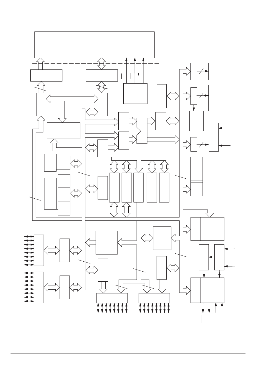
SECTION 3: SECURE MICROCONTROLLER
ARCHITECTURE
Introduction
The Secure Microcontroller family is based on an 8051
compatible core with a memory interface and I/O logic
build around it. Many functions are identical to standard
8051s and are documented here for completeness. In
general, most architecture features apply to all members of the Secure Microcontroller family. When there is
a difference between versions, this will be mentioned. A
block diagram of the microcontroller core is shown in
Figure 3–1 below.
Bus Organization
There are four major busses in the Secure Microprocessor: the Internal Data Bus, the Internal Address Bus, the
Byte–wide Memory Bus, and the Expanded Bus. All addresses and data which are transferred during program
execution are passed on the Internal Address and Data
Busses. User Program and Data Memory is always accessed from either the byte–wide Program/Data RAM
or from external memory located on the Expanded Bus.
The Byte–wide Memory Bus is used for access to Program/Data RAM in the same fashion as an 8051 Family
device would access internal ROM or EPROM memory.
This bus can be used in place of the Expanded Bus,
freeing Port 2 and Port 0 pins for general I/O use.
CPU Registers
All of the CPU registers are mapped as Special Function
Registers (SFR’s) and are identical in number and function to those present within the 8051. These registers
are described briefly below:
Accumulator
The Accumulator (A) is used as either a source or destination register in all arithmetic instructions. It may also
be used in most other types of instructions.
Stack Pointer
The Stack Pointer (SP) is an 8–bit register which is used
to mark the location of the last byte of data stored in the
stack. The stack itself may be located anywhere in the
on–chip 128–byte Scratchpad register area. The Stack
Pointer pre-increments during a stack push and postdecrements during a stack pop.
B Register
The major function of the B register is as a source and
destination register during multiply and divide instructions. It may also be used as a scratchpad register.
Program Status Word
The Program Status Word (PSW) contains status flags
that are set according to the results of a previously
executed instruction. In addition, the PSW contains register bank select bits.
Data Pointer
The Data Pointer (DPTR) is used to access Data
Memory that may be mapped into Byte–wide Data RAM
or onto external memory devices on the Expanded Bus.
It is accessed by the user’s program as either two 8–bit
Special Function registers or as a 16–bit register with
certain instructions.
Scratchpad Registers
Scratchpad registers are 128 registers where data may
be stored directly. They are addressed from 00H to 7FH
and may be accessed by a MOV instruction. Included in
the scratchpad area are four 8–byte banks of working
registers. These registers are not part of the data
memory map.
Serial I/O
The on–chip serial I/O port is comprised of a receive
data buffer , a transmit data buffer, and a control register .
Both the receive data buffer and the transmit data buffer
are accessed in a single location (SBUF) in the Special
Function Register map. The control register (SCON) is
accessed in an separate location. When the serial I/O
function is enabled, two external I/O pins (P3.0, P3.1)
are re–assigned in hardware to serve the transmit and
receive data functions.
Programmable Timers
Two 16–bit programmable timers are included that can
perform various timing and counting functions. A total of
four registers (TH1, TL1, TH0, and TL0) access the upper and lower halves of each of the two timer/counters.
A single control register (TCON) is used to select the
various operating modes of the two timers. Two external
I/O pins (P3.4, P3.5) may be programmed to serve as
external counter inputs, one pin for each of the two timer/counters.
7
050396 6/173
Page 8
USER’S GUIDE
SECURE MICROCONTROLLER ARCHITECTURAL BLOCK DIAGRAM Figure 3–1
DATA RAM
EXTERNAL
PROGRAM/
BUS
MEMORY
PC
INCREMENTOR
BYTE–WIDE
STACK
POINTER
PSW
PC
88
DRIVERSDRIVERS
15
ADDRESS
ENCRYPTOR
KEY
ENCRYPT
I/O
SBUF
SERIAL
INTERNAL ADDRESS BUS
TIMER
16
TIMER
SCON
TL0
TH0
0
TCON
TLMOD
1
TL1
TH1
8
DATA
ENCRYPTOR
ACC
B
REGISTER
DPTR
CE1
TEMP 1 TEMP 2
BUFFER
CE2
AND
TIMING
CONTROL
PROGRAM
ADDR. REG.
R/W
ALU
INTERNAL DATA BUS
TAMCONSECURITY
LOCK
LOGIC
PCON
CONTROL
INTERRUPT
IP
IE
LOGIC
TIMED
ACCESS
MEMORY
CTL. LOGIC
ALLOCATIONS
CONTROL
NONVOLATILE
VCC VLI
050396 7/173
PORT 3
DRIVERS
PORT 1
DRIVERS
128
REGISTER
SCRATCH–
TIMER
WATCHDOG
TIMING
REGISTER
ALE
PSEN
PAD
REGISTERS
OSCILLATOR
AND
CONTROL
EA
XTAL1 XTAL2
RST
IDR ADDR.
RAM
ROM
LOADER
INTERNAL DATA BUS
LATCH
PORT 3
8 8
LATCH
PORT 1
RESIDENT
LATCH
PORT 2
8
DRIVERS
PORT 2
INTERNAL ADDRESS BUS
16
8
VECTOR
LATCH
PORT 0
DRIVERS
PORT 0
INSTRUCTION
8
Page 9

USER’S GUIDE
Parallel I/O
Four SFR’s provide access for the four parallel I/O port
latches. These I/O ports are denoted as P0, P1, P2, and
P3. A total of 32 bits of parallel I/O is available through
these I/O ports. However, up to 16 bits are sacrificed
when the Expanded Bus mode is used to interface to external memory and up to six bits may be sacrificed if any
external interrupt inputs, timer counter inputs, or serial
I/O functions are used. When using the Byte–wide bus,
ports are not affected.
Program/Data RAM Interface
Secure Microcontrollers provide a non–multiplexed
Byte–wide bus that connects to external SRAM. They
also make this RAM nonvolatile, decode memory access for it, and write–protect portions designated as program memory. The Byte–wide bus consists of up to 16
address lines (depending on the version), eight data
lines, read/write control, and decoded chip enables.
When accessing the SRAM via its Byte–wide bus, there
is no activity on the ports. Thus if memory access is restricted to this bus, all ports are free for use by the
application. In module form, the microprocessor is already connected to SRAM via the Byte–wide bus making program and data memory access appear internal.
Secure Microprocessors can also access memory using the multiplexed Expanded Bus consisting of Port 0
and 2, WR (P3.6) and RD (P3.7). This is usually undesirable since it consumes port pins that can be used for
other activity. If Expanded bus access is desired, up to
64K ROM and 64K RAM can be accessed in the same
manner as a traditional 8051. Each version has different
provisions for using the Expanded bus, depending on
memory map and user’s configuration. These issues
are discussed under the Programmer’s Guide.
High–Reliability Circuitry
This feature ensures proper operation of the micro and
maintains the contents of the Program/Data RAM in the
absence of VCC using a self–contained lithium energy
source. The logic provided includes the Power Fail
Warning Interrupt, Automatic Power Down and Power
On Reset. As a result, the Program/Data RAM may be
modified whenever necessary during execution of the
user’s software but will remain unchanged when V
absent. The circuitry also maintains the Internal
CC
Scratchpad RAM and certain Special Function registers
during a power down condition.
Software Encryption Logic
DS5000 and DS5002 series parts provide software security circuits that include the Address Encryptor, Data
Encryptor, and the Encryption Key Word. When the device is operating in the Encryption mode and using the
Program/Data RAM, the Address Encryptor is used to
transform “logical” addresses on the Internal Address
Bus into encrypted addresses which appear on the
Byte–wide Memory Bus to the RAM. Similarly , the Data
Encryptor transforms data on the Internal Data bus into
encrypted data during write operations on the Byte–
wide Memory bus. When data is read back, the Data Encryptor restores it to its true value. Although each encryptor uses its own algorithm for encrypting data, both
depend on the Encryption Key Word stored on–chip.
Security Lock Logic
The Security Lock logic prevents a read or write to any
Program/Data RAM location using the bootstrap loader.
In addition, it inhibits the device from fetching code in the
Expanded Bus Mode. By disabling access to key internal resources, this feature precludes unauthorized disassembly of application software contained in Program/
Data RAM. In contrast with an EPROM security bit,
clearing the Security Lock wipes the entire RAM area.
Vector RAM
The Vector RAM is used to contain the reset and interrupt vector code when the Soft Microcontroller is operating in the Encryption mode. This feature is included to
insure the security of the application software. The operation of the Vector RAM as well as the reason for its
inclusion in the architecture are discussed in the
Software Security section.
Timed Access Logic
The Timed Access logic is used to protect against inadvertent changes to configuration and to the Program
RAM in the event of a loss of software control. The protected configuration parameters include the Partition
Address bits in the MCON register, as well as the Enable
Watchdog Timer bit, Stop Mode bit, and Power On Re-
is
set bit in the PCON register.
9
050396 8/173
Page 10

USER’S GUIDE
Watchdog Timer
When the user’s software is being executed, the Watchdog Timer can be used to automatically restart the processor in the event that software control is lost. It is also
used to generate an oscillator start–up delay to allow the
clock frequency to stabilize. This occurs during reset
cycles that follow a time in which the oscillator has been
stopped (Stop Mode Reset and Power On Reset).
Resident Loader ROM
The Resident Loader ROM contains firmware that controls the initial loading of the nonvolatile Program/Data
RAM. The firmware provides Serial Bootstrap Load operation via the on–chip serial port. The internal ROM is
not accessible by the user and performs the loading
function only when the device is strapped for operation
in the Program mode. The ROM becomes transparent
to the user once loading is complete and has no effect
on the memory map.
050396 9/173
10
Page 11
USER’S GUIDE
SECTION 4: PROGRAMMER’S GUIDE
The Secure Microcontroller uses nonvolatile RAM
technology for both Program and Data memory . It uses
NV SRAM in place of ROM by write protecting and decoding memory segments that a user designates as
cess a second RAM, but this was restricted to data
memory only. The DS5001 series can partition two
32K byte SRAMs, or even one 128K x 8 SRAM. Common elements of the programming model are given be-
low, with individual differences highlighted.
Program memory . The remaining RAM area is used as
nonvolatile data storage. One of the advantages of
breaking a common RAM into two segments is that a
smaller number of memory chips is needed. For example, if a system requires 24K bytes of program memory
and 4K bytes of data memory, this all fits within one
32K x 8 SRAM. The Secure Microcontroller can break
this RAM into program and data segments, unconditionally write protecting the program area. The process of
dividing the common memory space into ROM and
RAM is called partitioning. All Secure Microcontrollers
are capable of doing this. However, there are differences between original DS5000 series [includes
DS5000FP, DS5000(T), and DS2250T] and newer
DS5001 series [includes DS5001FP, DS2251T,
DS5002FP, DS2252T]. The original DS5000 series
could partition one SRAM of up to 32K bytes. It could ac-
Secure Microcontroller Memory
Organization
All Secure Microcontrollers follow the standard 8051
convention of three memory areas. These include Inter-
nal registers, Program memory and Data memory.
These memory areas are not contiguous and are ac-
cessed in different ways. The Secure Microcontroller
duplicates all standard 8051 registers and adds several
new ones. Secure Microcontrollers have a 64K byte
program and 64K byte data space. However, the
Secure Microcontrollers provide several ways to access
these areas, and these features are what make the fam-
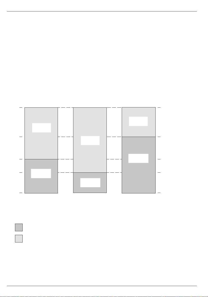
ily unique. Figure 4–1 shows the memory map of
Secure Microcontrollers in general terms. The specific
details and access to the memory areas are discussed
below.
SECURE MICROCONTROLLER MEMORY MAP Figure 4–1
–FFFFh–
64K
FFh
7Fh
00
SCRATCH PAD
REGISTERS
INTERNAL REGISTERS
SPECIAL
FUNCTION
REGISTERS
Internal Registers
The internal register space is divided into two parts.
These are Scratchpad Registers and Special Function
Registers (SFRs). There are a total of 128 Scratchpad
registers, commonly referred to as on–chip RAM. The
128 bytes include four 8–byte banks of working registers (R0–R7). The Scratchpad Registers are located at
register addresses 00–7Fh. This area is not located in
the Program or Data Memory area and is accessed by
0000
PROGRAM
MEMORY
DATA
MEMORY
different instructions. The Special Function Registers
(SFR) are located in the locations between 80h and
FFh. SFRs control the on–chip peripherals and memory
configurations. Direct addressing should be used to ac-
cess the SFR locations. If Register–Indirect addressing
is used, indeterminate data will be returned. Scratchpad
Registers are discussed immediately below, with SFR
descriptions following later in this section.
11
050396 10/173
Page 12
USER’S GUIDE
The Scratchpad Registers are general purpose data
storage RAM. They are commonly used for temporary
storage of a small number of variables when high–
speed access is needed. Off–chip RAM (MOVX) is
used when the quantity of data is larger than 128 bytes.
The Scratchpad Registers are lithium backed and will
be preserved in the absence of power.
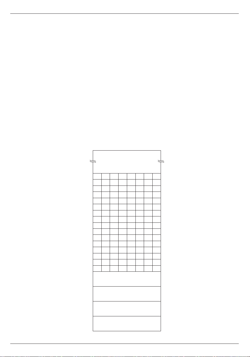
The Scratchpad area has two additional functions. First,
16 bytes of the Scratchpad area are bit addressable.
That is, while each byte has an address of its own, these
bits also have individual bit addresses. Certain instructions operate on bits instead of bytes. Although the addresses appear the same, the microprocessor can distinguish a bit address from a byte address by the
instruction used. A large number of individual software
flags and conditions can be represented using 128
(16*8) individually addressable bits.
SCRATCHPAD REGISTER MAP Figure 4–2
7FH
7F 7E 7D 7C 7B 7A 79 78
2FH
77 76 75 74 73 72 71 70
2EH
6F 6E 6D 6C 6B 6A 69 68
2DH
67 66 65 64 63 62 61 60
2CH
5F 5E 5D 5C 5B 5A 59 58
2BH
57 56 55 54 53 52 51 50
2AH
4F 4E 4D 4C 4B 4A 49 48
29H
47 46 45 44 43 42 41 40
28H
3F 3E 3D 3C 3B 3A 39 38
27H
37 36 35 34 33 32 31 30
26H
2F 2E 2D 2C 2B 2A 28 28
25H
27 26 25 24 23 22 21 20
24H
1F 1E 1D 1C 1B 1A 19 18
23H
17 16 15 14 13 12 11 10
22H
0F 0E 0D 0C 0B 0A 09 08
21H
07 06 05 04 03 02 01 00
20H
1FH
18H
17H
10H
0FH
08H
07H
00H
MSB LSB
A second use of the Scratchpad area is for the programmer’s stack. Like the 8051, the Secure Microcontroller
uses a Stack Pointer (SP – 81h) SFR to direct stack access into the internal registers. The SP has a default value of 07h. This means that stack storage will begin at
location 08h. Each PUSH or CALL instruction will increment the SP . Note that while the SP is located in the SFR
area, the stack itself is stored in the Scratchpad area.
The Scratchpad Register Memory map is shown in
Figure 4–2.
Programmer’s note
: with the use of ‘C’ compilers becoming more frequent, the large memory model should be examined. This compiler model places the
stack in off–chip SRAM. Secure Microcontroller based
systems usually have an abundance of such SRAM
compared to ROM based systems. While off–chip stack
results in slower execution time, the stack size becomes
virtually unlimited.
BANK 3
BANK 2
BANK 1
BANK 0
050396 11/173
12
Page 13

USER’S GUIDE
The 8051 instruction set allows efficient (single cycle)
access to variables when using the Working Registers.
These are a group of four 8–byte banks of Scratchpad
RAM. The active Working Registers are referred to as
R0–R7. They reside between location 00h and 1Fh, depending on which bank is currently selected. Two bits in
and R0 (PSW.3) are used to determine which is the active bank. Once selected, all instructions involving
R0–R7 will be directed to the selected group of 8 bytes.
This scheme also allows for a fast context switch by
simply changing banks. The following Table shows the
operation of the Register Bank selection.
the Special Function Register PSW called R1 (PSW.4)
PSW.4–3 ; R1–R0
Register Bank Select Used to select an 8–byte bank of registers to be assigned as R0–R7.
R1 R0 BANK STARTING ADDRESS (R0)
0 0 00h
0 1 08h
1 0 10h
1 1 18h
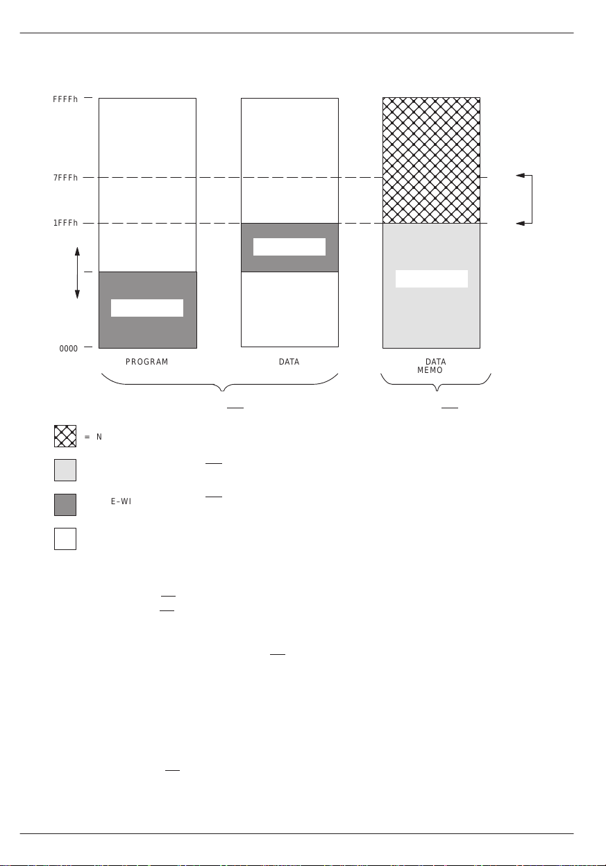
Program and Data Memory
The Secure Microcontroller divides its main memory between Program and Data segments. Each map consists
of a 64K byte area from 0000h to FFFFh. Program
memory is inherently read only, since there are no 8051
must be ROM/EPROM and data memory must be volatile SRAM. If NV RAM is needed on the Expanded bus,
then it must be externally backed up and write protected. The Secure Microcontroller makes no special
provisions for NV RAM on the Expanded bus.
instructions that write to this segment. Data memory is
read and write accessible without restrictions. The CPU
automatically routes program fetches to the program
area and MOVX instructions to the data memory area.
All of these elements are in common with the standard
8051. Secure Microcontroller differences lie in the
memory interface, memory map control, and flexibility of
the memory resources.
When discussing memory addressing of Secure Micro-
controllers, there are two important terms that are used
frequently: Partition and Range. The Partition is the
user–selectable address that divides the program seg-
ment from the data segment in a common RAM area on
the Byte–wide bus. The Partition is a user–adjustable
boundary that can be selected during Bootstrap Load-
ing or on the fly by the application software. The Range
Secure Microcontrollers provide two separate buses for
memory access. First is a Byte–wide address/data bus
is the total amount of memory connected to the Byte–
wide bus. This is set once during initial programming.
which is new to the 8051 architecture. This bus also provides a switched supply output that make standard
SRAM into nonvolatile memory , decoded chip enables,
and a R/W strobe. Furthermore, the Byte–wide bus
allows nonvolatile RAM memory to be divided between
Program and Data segments. When using a segment of
the RAM as Program Memory, this area can be loaded
using the Bootstrap Loader function described later in
this book.
The DS5000 series devices can access between 8K
and 64K bytes of NV RAM on the Byte–wide bus. Up to
the first 32K bytes are Partitionable into Program and
Data segments as described above. The DS5001 se-
ries can access between 8K and 128K bytes on its
Byte–wide bus with better Partition control. The
Memory map control resides in the MCON (address
C6h) Special Function Register on DS5000 devices. On
DS5001 devices, both the MCON (address C6h) and
Second is an Expanded bus constituted by Ports 0 and
2. This is the standard 8051 compatible memory bus
which is available as an option, but is not needed in
most cases. Program memory on the Expanded bus
RPCTL (address D8h) registers are used. Since the
memory maps and control have significant differences
between these versions, they are described below in
separate sections.
13
050396 12/173
Page 14

USER’S GUIDE
DS5000 Series Memory Organization
As mentioned above, the DS5000 series consists of the
DS5000FP chip and the DS5000(T) and DS2250T modules. The programming model discussed in this section
applies to all of these parts. The DS5000 series Byte–
wide bus has 15 address lines, eight data lines, a R/W
strobe, and two chip enables to access nonvolatile
RAM. In the case of a module, these are already connected and may be thought of as internal or embedded
memory. The DS5000 series can use either 8K x 8 or
32K x 8 SRAMs. The user must inform the microcontroller of the selected RAM size using the Range function.
The Range bit resides in the MCON SFR at MCON.3
and has a value of 0 when 8K SRAM is used and 1 when
a 32K byte SRAM is used. Range is selected during
Bootstrap Loading and can not be varied by the application software. The DS5000 device accesses memory on
its Byte–wide bus using two chip enables. The first,
, is Partitionable. That is, the RAM connected to
CE1
CE1, whether 8K or 32K, can be divided between program and data segments. The Partition is user–selected and can be set during Bootstrap Loading and by
software. Partitions are generally available on 2K byte
boundaries in the DS5000 except for the last which is
4K. The Partition is selected using the MCON SFR described below. CE2
The RAM on CE2
Access to CE2
switch. Bit 2 (ECE2) of the MCON SFR controls access
to CE2 and is described below.
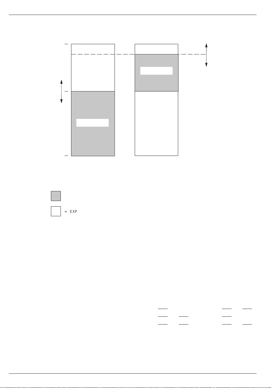
Figure 4–3 illustrates the functional memory map of a
DS5000 series device. The Partition, Range, ECE2,
and the logical address combine to determine whether
the DS5000 uses its Byte–wide bus or the Expanded
is restricted to data memory only.
should be of the same size as CE1.
is manual, and functions like a bank
Bus. Nonvolatile RAM access will occur when the logical address lies in one of the shaded regions. These are
program addresses below the Partition address, data
addresses above the Partition and below the Range address, or data addresses between 0 and the Range
when ECE2 is set to a logic 1. Note that when using
ECE2 to force data access, the CE2
RAM will be selected instead of the CE1 RAM. This means that on a
DS5000 module or a DS2250 with less than 64K RAM,
no data memory exists under CE2. The ECE2 has no
affect on program memory, which continues from the
RAM or the Expanded bus normally.
CE1
Note that the Partition and Range settings are not automatically linked. This means a user should take care not
to select a Partition that is larger than the Range. Naturally when the Range is 32K, the Partition address can
be as high as 32K. When a Range of 8K is used, Partition addresses below 8K should be used. Any address
that does not map onto the Byte–wide bus will be automatically be routed to the Expanded Bus of Ports 0 and
2. For module users. this means that any address not
routed to internal memory will go to the ports. The following examples will help illustrate the decoding.
When the Partition is at 3000h, and the Range at 32K,
program memory below 3000h is accessed on the
Byte–wide bus. Program memory at or above 3000h is
directed to the Expanded bus or Ports 0 and 2. When the
Partition is at 5800h and the Range at 32K, data
memory at 0000h is accessed on Ports 0 and 2. Data
memory at 6000h is located in NV RAM on the Byte–
wide bus. When the Partition is at 1000h and the Range
at 8K, all memory access above 1FFFh is on the Expanded bus. Below 8K, the Partition rules apply .
IMPORTANT APPLICATION NOTE
The MCON register is a special function register unique to Dallas Semiconductor microcontrollers which contains
nonvolatile memory configuration information. This register should be set to the desired value before loading the
device via the bootstrap loader. Failure to correctly configure the MCON register can cause the device to operate
incorrectly, including symptoms which appear similar to a defective device. Because this register is nonvolatile, incorrect memory settings will be preserved when power is removed. The DS5001FP, DS5002FP, DS2251T, and
DS2252T store additional memory configuration information in the RPCTL register, which should also be set to the
desired value before loading the device via the bootstrap loader.
050396 13/173
14
Page 15
DS5000 SERIES MEMORY MAP Figure 4–3
FFFFh
USER’S GUIDE
ECE2=1ECE2=0
64K
7FFFh
1FFFh
BYTE–WIDE
BUS ACCESS
PARTITION
ADDR.
BYTE–WIDE
BUS ACCESS
0000
LEGEND:
= NO MEMORY ACCESS
=
=
= EXPANDED BUS ACCESS ON PORTS 0 AND 2
PROGRAM DATA DATA
MEMORY MEMORY MEMORY
DEVICE #1 SELECTED
WITH CE1
BYTE–WIDE ACCESS WITH CE2
(NONVOLATILE RAM)
BYTE–WIDE ACCESS WITH CE1
(NONVOLATILE RAM)
The above memory map covers the standard operating
case. There are two conditions that can modify this
memory map. The first is the EA pin. The second is the
Security Lock. When the EA
pin is grounded, the
DS5000 will force all memory access to the Expanded
bus. This causes the DS5000 to behave like an 8031 regardless of the Partition, Range, or ECE2. The EA
should be pulled to +5V for normal operation. The second modifier is the Security Lock. When set, the Security Lock prevents using the Bootstrap Loader to read
the contents of the NV RAM. For security purposes, it
also prohibits program memory access on the Expanded Bus. Thus all program fetches must be restricted to
the Byte–wide bus when locked. The Security Lock
overrides the condition of the EA
pin as well.
32K
RANGE
ADDR.
8K
BYTE–WIDE
BUS ACCESS
DEVICE #2 SELECTED
WITH CE2
The selection of memory map controls provide unprecedented flexibility to configure a system. However, it is
possible to select contradictory settings. The micro will
compensate for these as follows. The Partitioning function allows a user to select the quantity of program and
data memory . It is possible to select all data and no program in NV RAM by choosing a Partition of 0000h. This
is a valid selection. However, using this setting and the
Security Lock is a conflict. This condition asks the micro
to use all program memory on the Expanded bus, but
also to prohibit the use of program memory on the Expanded bus. In this event, special circuits will automatically force the Partition to a location of 7FFFh. This
means all 32K memory on the Byte–wide bus is designated program memory. The second contradictory
15
050396 14/173
Page 16

USER’S GUIDE
case is to select a Range of 8K, and to choose a Partition of greater than 8K. This will result in the Range as
the limiting factor. Addresses above the Range will automatically be deflected to the Expanded bus. No data
memory will be allocated in NV RAM for this configura-
tion, the Partition can be selected or modified by the application software and CE2
is normally software controlled. However, in either case, the MCON SFR is used
to choose these settings. The MCON is summarized in
the SFR section below, but appears here also.
tion.
DS5000 Memory Map Control
The Partition and Range can be selected using the
Bootstrap Loader discussed in a later section. In addi-
DS5000 SERIES MCON REGISTER Figure 4–4
Bit Description:
MCON.7–4: PA3–0
“Partition Address”: Use to select the starting address of Data Memory in Embedded RAM. Pro-
gram space lies below the Partition address.
Selection:
PA3 P A2 PA1 PA0 Partition Address
0 0 0 0 0000H
0 0 0 1 0800H
0 0 1 0 1000H
0 0 1 1 1800H
0 1 0 0 2000H
0 1 0 1 2800H
0 1 1 0 3000H
0 1 1 1 3800H
1 0 0 0 4000H
1 0 0 1 4800H
1 0 1 0 5000H
1 0 1 1 5800H
1 1 0 0 6000H
1 1 0 1 6800H
1 1 1 0 7000H*
1 1 1 1 8000H*
*A 4K byte increment (not 2K bytes) in the Partition Address takes
place between bit field values 1110B and 1111B.
Initialization: Set to all 1’s on a No V
Power On Reset or when the Security Lock bit is
LI
cleared to a 0 from a previous 1 state. These bits are also set to all 1’s when
any attempt is made to have them cleared to all 0’s with the SL bit set to a 1
(illegal condition).
Read Access: May be read anytime.
Write Access: PAA bit must = 1 in order to write PA3–0. Timed Access is not required to
write to PA3–0 once PAA = 1.
050396 15/173
16
Page 17

USER’S GUIDE
MCON.3: RA32/8
“Range Address”: Sets the maximum usable address on the Byte–wide bus.
RA32/8 = 0 sets Range Address = 1FFFH (8K); RA32/8 = 1 sets Range Address = 7FFFH (32K)
Initialization: Set to a 1 on a No V
Power On Reset and when the Security Lock bit (SL) is
LI
cleared to a 0 from a previous 1 state. Remains unchanged on all other types
of resets.
Read Access: May be read normally anytime.
Write Access: Cannot be modified by the application software; can only be written during
Program Load mode.
MCON.2: ECE2
“Enable Chip Enable 2”: Used to enable or disable the CE2
signal to additional RAM Data Memory
space. This bit should always be cleared to 0 in the DS5000–8, DS5000–32,
DS2250–8, and DS2250–32 versions.
Initialization: Cleared to 0 only during a No V
Power On Reset.
LI
Read Access: Read normally anytime.
Write Access: Can be written normally anytime.
MCON.1: PAA
“Partition Address Access”: Used to protect the programming of the Partition Address select bits. PA3–0
cannot be written when PAA=0. PAA can be written only via the Timed Access register.
Initialization: PAA is cleared on a reset.
Read Access: PAA may be read anytime.
Write Access: The Timed Access register must be used to perform any type of write opera-
tion on the PAA bit.
DS5001/DS5002 Memory Organization
As mentioned above, the DS5001/DS5002 series consists of the DS5001FP chip, the DS2251T module, the
DS5002FP chip, and the DS2252T module. Note that the
DS5002FP is a high security version of the DS5001FP,
but has the same memory map and I/O. The programming model discussed in this section applies to all of
these parts and any reference to the DS5001 applies to
all of them. The DS5001 series Byte–wide bus has 16
address lines, eight data lines, a R/W
of eight chip enables to access nonvolatile RAM and peripherals. Chip enables include CE1 – CE4 and PE1 –
PE4. The four chip enables (CE1–4) are for nonvolatile
RAM access. How they are connected depends on the
memory mode and the selection of SRAMs. The PE signals are generally for memory mapped peripherals, but
can be used for more RAM if desired. PE1 and PE2 are
strobe, and a total
lithium–backed, PE3
and PE4 are not. In the case of a
module, PE1 may be connected to a real–time clock.
Memory map control resides in the MCON (C6h) and
RPCTL (D8h) registers. The MCON register has selected differences from its DS5000 counterpart. These
are documented below . The RPCTL is not present in the
DS5000. Also, not all of the bits in this register pertain to
memory map control. This section describes the relevant bits and the SFR section below documents the entire register.
The DS5001 series can use multiple 8K x 8 or 32K x 8
SRAMs or a single 128K x 8 SRAM. These parts can operate in either a Partitionable (like DS5000) or non–
partitionable mode. The mode is selected via the PM
(MCON.1) bit of the MCON register. Note, the DS5001
MCON provides different functions than the DS5000. In
17
050396 16/173
Page 18

USER’S GUIDE
a Partitionable mode (PM=0), the DS5001 can use up
to 64K x 8 SRAM for program and data on its Byte–wide
bus. It can partition this area into program and data
segments on 4K boundaries. The 64K memory space
would consist of two 32K x 8 SRAMs. Each is accessed
by a separate chip enable (CE1
and CE2), but the microcontroller automatically decodes which is needed.
While the DS5001 can use between one 8K x 8 SRAM
and 4 32K x 8 SRAMs, it does not automatically know
RG1 RG0 RANGE CE1
ACCESS CE2 ACCESS
which configuration is used. The Range function deter mines how much total memory is connected to the
Byte–wide bus. The user must identify the total RAM
size using the Range bits RG1 and RG0. RG1 is located at MCON.3 and RG0 is located at RPCTL.0.
These Range bits are selected during the Bootstrap
Loading process and can not be modified by the application software. The Table below shows the Range
values that can be selected when PM=0 (Partitionable).
1 1 64K 0000–7FFFh 8000–FFFFh
1 0 32K 0000–7FFFh NA
0 1 16K 0000–1FFFh 2000h–3FFFh
0 0 8K 0000–1FFFh NA
The total RAM space is partitionable, regardless of
which Range is selected. This contrasts with the
DS5000 that allowed partitioning of CE1
only. The
Partition table is shown below. P A3–0 are the four MSBs
of the MCON register (MCON.7–4). Note that the Parti-
a Range of less than 64K is selected, then the partition
settings above the Range should not be unused. The
microcontroller automatically decodes which RAM to
enable, and uses the Partition to decide if this is program memory or data memory.
tion values do not scale depending on Range. That is, if
PA3 PA2 PA1 PA0 P ARTITION BYTE–WIDE BUS MEMORY MAP
0 0 0 0 0000h 0K PROGRAM, DATA = RANGE
0 0 0 1 1000h 4K PROGRAM, DATA = RANGE – 4K
0 0 1 0 2000h 8K PROGRAM, DATA = RANGE – 8K
0 0 1 1 3000h 12K PROGRAM, DATA = RANGE – 12K
0 1 0 0 4000h 16K PROGRAM, DATA = RANGE – 16K
0 1 0 1 5000h 20K PROGRAM, DATA = RANGE – 20K
0 1 1 0 6000h 24K PROGRAM, DATA = RANGE – 24K
0 1 1 1 7000h 28K PROGRAM, DATA = RANGE – 28K
1 0 0 0 8000h 32K PROGRAM, DATA = RANGE – 32K
1 0 0 1 9000h 36K PROGRAM, 28K DATA
1 0 1 0 A000h 40K PROGRAM, 24K DATA
1 0 1 1 B000h 44K PROGRAM, 20K DATA
1 1 0 0 C000h 48K PROGRAM, 16K DATA
1 1 0 1 D000h 52K PROGRAM, 12K DATA
1 1 1 0 E000h 56K PROGRAM, 8K DATA
1 1 1 1 FFFFh 64K PROGRAM, 0K DATA
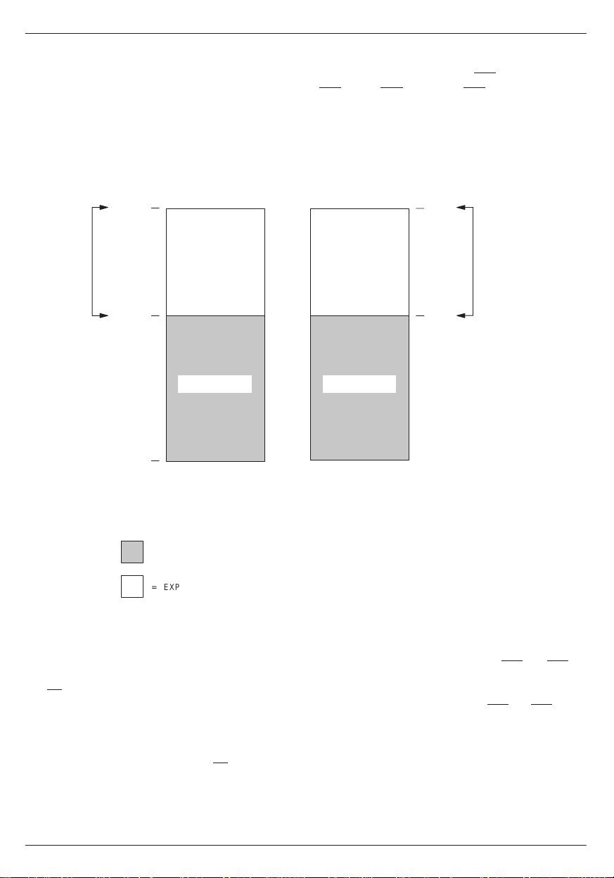
Figure 4–5 illustrates the functional memory map of a
DS5001 series device in Partitionable mode. Note that
like the DS5000, any access that does not correspond
050396 17/173
to a Byte–wide bus location is routed to the Expanded
bus Ports 0 and 2.
18
Page 19
PARTITIONABLE MEMORY MAP FOR DS5001/DS5002 SERIES Figure 4–5
FFFFh
PARTITION
ADDR.
0000
LEGEND:
BYTE–WIDE
BUS ACCESS
PROGRAM DATA
MEMORY MEMORY
BYTE–WIDE ACCESS
=
(NONVOLATILE RAM)
PES=0
BYTE–WIDE
BUS ACCESS
64K
RANGE
ADDRESS
USER’S GUIDE
= EXPANDED BUS ACCESS ON PORTS 0 AND 2
The non–partitionable mode allows the maximum
amount of memory to be used on the Byte–wide bus. A
non–partitionable mode would be used because the
8051 architecture is restricted to a total of 64K program
and 64K data (without bank switching). This means that
if the maximum amount of either program or data (or
both) is needed, partitioning can not be done. The
DS5001/DS5002 series accommodates these situations with four selections of non–partitionable (PM=1)
the Range bits when PM=1. Also note the MSEL signal.
This is a pin on DS5001/DS5002 series devices that
tells the processor whether multiple 32K RAMs or a
128K RAM is being used. When MSEL=0, a single 128K
device is used. It is not possible to partition the device
when MSEL=0, and the state of the partition bits will be
ignored. The four selections are as follows. The non–
partitionable memory map is shown in Figure 4–6.
Byte–wide bus segments begin at 0000h.
memory control shown below. These are selected using
MSEL RG1 RG0 PROGRAM DATA PROGRAM ACCESS DATA ACCESS
1 0 0 32K 64K 1 @ 32K, CE1 2 @ 32K, CE3 and CE4
1 0 1 64K 32K 2 @ 32K, CE1 and CE2 1 @ 32K, CE3
1 1 0 64K 64K 2 @ 32K, CE1 and CE2 2 @ 32K, CE3 and CE4
0 1 1 64K 64K 1 @ 128K X 8, for both program and data
19
050396 18/173
Page 20
USER’S GUIDE
Any address that does not fall into the Byte–wide bus
area is routed to the Expanded bus of Ports 0 and 2. This
could only occur for the first two settings. Note that a
single 128K device is the least expensive in terms of
component cost and size. In this case, all memory addressable by the DS5001 is stored in a nonvolatile
128K x 8 SRAM. When the MSEL pin is grounded, the
device automatically converts CE1
CE2 to A16, CE3 to A15, and CE4 is unused. The MSL
bit, accessible only via the bootstrap loader, is used to
select whether the the 64KB data or 64KB program segment is addressed by the loader.
NON–PARTITIONABLE MEMORY MAP FOR DS5001, DS5002 SERIES Figure 4–6
PES=0
BYTE–WIDE
BUS ACCESS
64K
RANGE
32K7FFFh
PROGRAM
RANGE
FFFFh
0000
BYTE–WIDE
BUS ACCESS
PROGRAM DATA
MEMORY MEMORY
to a chip enable,
DATA
LEGEND:
BYTE–WIDE ACCESS
=
(NONVOLATILE RAM)
= EXPANDED BUS ACCESS ON PORTS 0 AND 2
DS5001/DS5002 Memory Mapped
Peripherals
The DS5001 series provides four decoded chip enables
that can be used for peripheral access or extra RAM on
the Byte–wide bus. Application software enables the
four PE signals, which are decoded on 16K byte boundaries. While they are enabled, they completely use the
data memory map and normal data memory is not available on either the Byte–wide or Expanded bus. The PES
bit (MCON.2) is set to a logic 1 to access the peripheral
space. When PES=1, the appropriate PE
activated based on the logical address. Figure 4–7
050396 19/173
signal will be
shows the data memory map while PES=1. PES has an
identical effect for either Partitionable or Non–partitionable modes. It has no effect on the program area. Note
that the first two Peripheral Enables, PE1
and PE2 are
lithium backed by the DS5001. This means that when
is removed, the device will maintain these chip en-
V
CC
ables in a logic high, inactive state. PE3 and PE4 are not
lithium backed making them suitable for UARTs, A/Ds,
etc. Lithium backed chip enables are used to access
lithium backed memory or peripherals, including the
DS1283 real–time clock used in the DS2251T and
DS2252T.
20
Page 21
USER’S GUIDE
On occasion, a memory mapped peripheral is needed
that interfaces directly to an 8051 multiplexed bus.
When this occurs, MOVX instructions can be forced to
use the Expanded bus in any mode with the EXBS bit
(RPCTL.5). Setting this bit to a logic one forces all
MOVX instructions to the Expanded bus. While
EXBS=1, the entire 64K data memory map is accessed
in this way. Clearing EXBS will cause the microcontroller to revert to its selected configuration. In most systems, the EXBS bit will not be used.
PERIPHERAL ENABLES IN THE DATA MEMORY MAP Figure 4–7
64K
PES=1
PE4
PE3
PE2
PE1
0
DATA
MEMORY
FFFFh
BFFFh
7FFFh
3FFFh
DS5001/DS5002 Memory Map Control
Like the DS5000, the DS5001/DS5002 uses Special
Function Registers to control the memory map. The
memory control functions include the Partition, Range,
Partition Mode (PM), Expanded Bus Select (EXBS), Peripheral Enable Select (PES) and Access Enable (AE –
discussed below). The Partition and Range can be selected using the Bootstrap Loader discussed in a later
section. In addition, the Partition can be selected or modified by the application software by writing to the
MCON register. PES is normally used by software and is
also controlled by the MCON register. The MCON is
documented in the SFR summary, but also appears
here for convenience. The Range is controlled by a
combination of MCON and RPCTL bits. In addition, the
EXBS and AE are controlled using the RTPCL register .
As not all of the RPCTL bits pertain to memory control,
the relevant bits are described below. RPCTL is fully
documented in the SFR summary.
050396 20/173
21
Page 22

USER’S GUIDE
DS5001/DS5002 SERIES MCON REGISTER Figure 4–8
PA3 PA2 PA1 PA0 RG1 PES PM –––
Bit Description:
MCON.7–4: PA3–0
Initialization: Unaffected by watchdog, external, or power–up resets. Set to 1111B on a
Read Access: Can be read normally at any time.
Write Access: Timed Access Protected. Also, cannot be written by the application soft-
Partition Address. When PM=0, this address specifies the boundary
between program and data memory in a continuous space.
reset.
No V
LI
ware if set to 0000B by the serial loader. If a 0000B is written via the serial
loader and the security lock is set, the Partition will become 1111B. The
same will occur if write access is available and application software writes a
0000B. In addition, these bits will be set to 1 1 1 1B if security lock is cleared.
MCON.3: RG1
One of two bits that determine the range of program space. RG0 is located
in the RPCTL register.
Initialization: Unaffected by watchdog, external, or power–up resets. Set to 1 on a No V
reset or a clearing of the security lock.
Read Access: Can be read at any time.
Write Access: Cannot be modified by the application software. Can only be written during
program load.
MCON.2: PES
Peripheral Enable Select. When this bit is set, the data space is controlled
by PE1 – PE4. Peripherals are memory–mapped in 16K blocks, and are
accessed by MOVX instructions.
Initialization: Cleared by all resets.
Read Access: Can be read at any time.
Write Access: Can be written at any time.
MCON.1: PM
Partition Mode. When PM=0, a partitionable, continuous memory map is
invoked. When PM=1, one of four fixed allocations is used.
Initialization: Unaffected by watchdog, external, or power–up reset. Cleared on a No V
reset.
Read Access: Can be read at any time.
Write Access: Cannot be written by the application software. Can only be modified during
program load.
LI
LI
050396 21/173
22
Page 23

DS5001/DS5002 SERIES RPCTL REGISTER BITS AFFECTING MEMORY Figure 4–9
RNR ––– EXBS AE IBI DMA RPCON RG0
Bit Description:
RPCTL.5: EXBS
The Expanded Bus Select routes data memory access (MOVX) to the
Expanded bus formed by ports 0 and 2 when set.
Initialization: Cleared after all resets.
Read Access: Can be read at any time.
Write Access: Can be written at any time.
USER’S GUIDE
RPCTL.4: AE
Access Enable is used when a software reload is desired without using
Program Load mode. When set, the DS5001 will be temporarily configured
in a Partitionable configuration with the partition at 4K. This will occur even
if the PM=1. When cleared, the prior memory configuration is resumed.
Initialization: Cleared after all resets.
Read Access: Can be read at any time.
Write Access: Can be written at any time, timed access protected.
RPCTL.0: RG0
This is a Range bit which is used to determine the size of the program
memory space. Its usage is shown above.
Initialization: Unaffected by watchdog, external, or power–up resets. Cleared on a No V
reset or clearing of the security lock.
Read Access: Can be read at any time.
Write Access: Cannot be modified by the application software. Can only be written during
Program Load.
Loading and Reloading Program Memory
Soft Microcontrollers are programmed through a built–
in Bootstrap Loader function. This loader is also used to
configure the desired options for memory map control.
device, the Bootstrap Loader must be invoked. However, the Secure Microcontroller is designed to allow a
partial reload of memory without invoking the Bootstrap
Loader.
The Secure Microcontroller uses its low power lithium
backed circuits to maintain critical settings in the absence of power. For this reason, it is not necessary to set
the Partition, Range, etc. after every power–up or reset.
Once set, they will remain unless deliberately modified.
Bootstrap Loading is discussed in a later section. One
of the major advantages of a Secure Microcontroller is
the ability to change these settings, and even reload the
entire program memory while the device is installed in
system. To completely re–program and re–configure a
The major advantage of this technique is that it requires
no hardware or external switches. Most of the memory
can be reprogrammed under application software con-
trol. It would commonly be used when the target system
connects to a PC through a serial port as part of an ap-
plication. For example, a data logger that must dump
memory periodically. While connected to the PC, it is
extremely easy to reload portions of memory using the
“Soft Reload”.
LI
23
050396 22/173
Page 24

USER’S GUIDE
Application software always has unrestricted read/write
access to the nonvolatile RAM designated as data
memory. This is the memory that lies above the Partition
address and below the Range address (the non–partitionable configuration of the DS5001 will be addressed
separately). Data memory is read or written using the
MOVX instruction. Only the area designated as program memory can not be altered. The key to doing a
“Soft Reload” is to temporarily change the program
memory RAM into data memory. Using an SFR, the application software can authorize the Secure Microcontroller to temporarily redefine a portion of the program
memory area as data memory. Once this is done, the
new code can be received through a serial port (or other
means) and written into data memory. When the process is complete and the new memory is verified as correct, software converts the RAM back into write–protected program memory for the duration. As with the
memory map control, there are minor differences between the DS5000 series and DS5001/DS5002 series
devices in how this is accomplished. Each is described
below.
SOFT RELOAD OF A DS5000 SERIES DEVICE
When application software decides that it should repro-
gram a portion of memory, the software must convert
the target area into data memory. The DS5000 will do
this when software sets the PAA bit (MCON.1) to a logic
1. PAA is the Partition Access Enable. Setting PAA has
two effects. The microcontroller will automatically move
the Partition to 0800h and allow write access to the
Partition control bits PA3–0 (MCON.7–4). At this time,
the software can adjust the Partition, but the new value
will not be used until after PAA is cleared. The Partition
remains at 0800h as long as P AA=1, regardless of the
Partition control bits. This leaves a 2K block of NV RAM
(from 0000–0800h) assigned as program memory.
Apart from this, no other changes take place and software continues to operate normally. Caution, make certain that the code that controls the PAA resides in this
first 2K. When PAA=1, all addresses on the Byte–wide
bus greater than 0800h will be viewed as data memory
and can not be executed even if they were program
memory originally. This gives the software read/write
access to the remaining 6K bytes (Range=8K) or 30K
bytes (Range=32K) of NV RAM on the Byte–wide bus.
At this time, software can begin reloading the target
area of memory. There are two minor variations of this
procedure. First, a user’s loader routine that resides
below 0800h (2K) can reprogram the remainder of
memory as needed. This is done be receiving the new
code through a serial port or other mechanism and writing it to the RAM at the addresses where it will be
executed. Since the RAM is data memory , the write operation is done using MOVX instructions.
The second option is that the user’s code below 2K can
simply move the Partition to a new value. This is done by
writing a new value for PA3–0 in MCON (MCON.7–4)
while PAA is still set to a 1, then clearing PAA. The purpose of this would be that the loader routine mentioned
in option 1 resides in memory above 2K, but below the
target memory area. T o gain access, the Partition must
be moved to a location that includes this loader routine.
Once the Partition is moved to this temporary location,
the software loader can reprogram new code as before.
When loading is complete, the Partition must be either
restored or set to a new value that is appropriate for the
new software. If the PA3–0 bits were not modified, then
the PAA bit can simply be cleared. This will cause the old
Partition to be restored. If the PAA3–0 were modified
during loading or software has grown significantly , then
a new Partition is needed. The PA3–0 bits must be written while PAA is set to a 1.
The DS5000FP protects the PAA bit from accidental
modification by requiring a Timed Access procedure.
Timed Access is designed to prevent an out–of–control
program from modifying the PAA bit and crashing the
application. Timed Access is discussed in a later section. To summarize the “Soft Reload”, the procedure
goes as follows:
1. Ensure that current program execution is in the
range of 0000h to 0800h.
2. Set the Partition Address Access (PAA) bit using a
Timed Access Procedure.
3. Load new contents into program memory at addresses above 0800h using MOVX instructions.
4. Define a new Partition address if necessary and
write the appropriate bits into PA3–0 in the MCON
SFR.
5. Restore the current Partition by clearing the PAA bit
with a Timed Access procedure.
6. Resume operation.
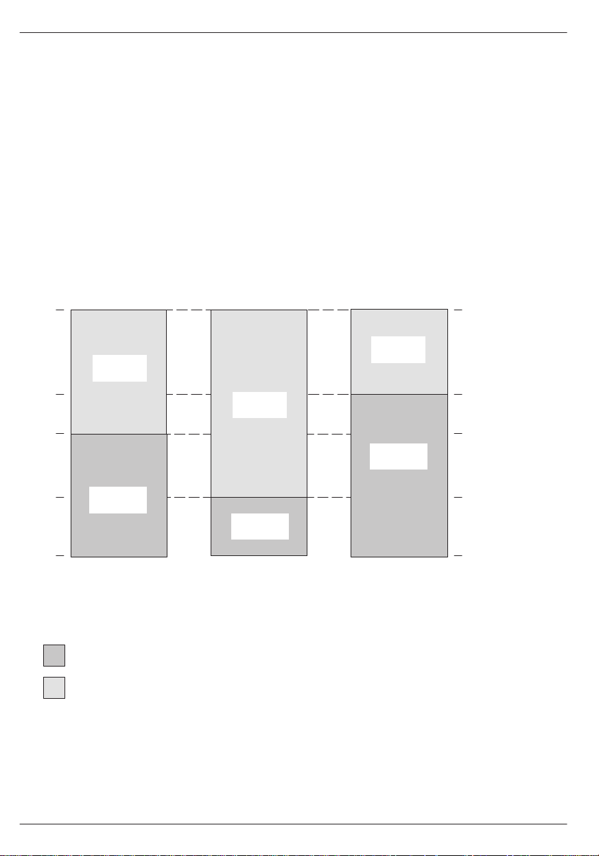
The following illustrates the Soft Reload procedure. The
original program requires a partition of 4000h (16K bytes). The new program is larger, requiring a Partition of
6000h (24K bytes). The code that performs these steps
is shown below. This routine must be located below
0800h in program memory .
050396 23/173
24
Page 25
MOV TA, #0AAh ; TIMED ACCESS
MOV TA, #55h ; TIMED ACCESS 2
MOV MCON, #10001010b ; SET PAA BIT
. ; USER’S CODE TO LOAD
. ; RAM USING MOVX
.
.
MOV TA, #0AAh ; TIMED ACCESS
MOV TA, #55h ; TIMED ACCESS 2
MOV MCON, #11001000b ; LOAD NEW PARTITION AND CLEAR PAA BIT
RELOADING PORTIONS OF A DS5000 SERIES DEVICE Figure 4–10
7FFFh
DATA
MEMORY
SPACE
PROGRAM
MEMORY
SPACE
6000h
4000h
DATA
MEMORY
SPACE
DATA
MEMORY
SPACE
USER’S GUIDE
RANGE (32K)
NEW PARTITION (24K)
OLD PARTITION (16K)
0800h
0000h
LEGEND:
PROGRAM
MEMORY
SPACE
BEFORE LOADING
PAA=0
PA3–0=1000b
NONVOLATILE RAM PROGRAM MEMORY
=
=
NONVOLATILE RAM DATA MEMORY
PROGRAM
MEMORY
SPACE
DURING LOADING
PAA=1
PA3–0=XXXXb
25
AFTER LOADING
PAA=0
PA3–0=1100b
TEMP PARTITION (2K)
0K
050396 24/173
Page 26

USER’S GUIDE
SOFT RELOAD OF A DS5001/DS5002
When application software decides that it should repro-
gram a portion of memory, the software must convert
the target area into data memory. However, a Soft Reload of a DS5001 series device has minor variations
from the DS5000 version. First, there is no PAA bit in the
DS5001. If the DS5001 is in a Partitionable mode then
the user’s program must manipulate the Partition control bits PA3–0, placing the Partition to a value that permits the target area to be loaded. Moving the Partition to
a new value should convert the target area to data
memory allowing read/write access. The user’s loader
routine then uses MOVX instructions to load the new
program contents into memory . This program can be received from a serial port or other mechanism. When the
loading procedure is complete, a new Partition (or the
old one) must be loaded. Note that the loader routine
must reside below the Partition at all times.
In the DS5000 series, the PAA bit was protected by a
Timed Access procedure. In the DS5001, the PA3–0
bits are protected directly. The user’s program must use
a Timed Access procedure to alter these bits. The microcontroller further protects the application by not permitting software to write a 0000b into P A3–0. This would
cause a program memory area of 0K. Timed Access is
discussed in a later section.
If the device is in a non–partitionable configuration, then
an extra step is required. T o perform a Soft Reload of the
program contents in a non–partitionable mode, the software must convert the micro to a Partitionable mode
temporarily . The Access Enable bit (RPCTL.4) will accomplish this. Setting the AE bit to a logic 1 converts the
DS5001 into a Partitionable mode for as long as it is set.
This means that regardless of the original setting, once
AE=1, the memory map is a 64K partitionable mode.
The Partition is set to 1000h (4K) when AE=1, so the
loader routine must reside in this area. The user can
then perform the Soft Reload as discussed above.
When loading is complete, the software should clear the
AE bit. Note that AE requires software to use a Timed
Access procedure to alter it. This method allows a user
to alter program memory in a non–partitionable mode.
Data memory can be initialized by application software
at any time. Since full read/write access is available, no
special provisions are needed.
T o summarize the “Soft Reload” for a DS5001/DS5002,
the procedure goes as follows:
Partitionable mode
1. Write a value to PA3–0 using a Timed Access that
gives access to the target area of memory.
2. Load new contents into program memory at addresses above the Partition using MOVX instructions.
3. Define a new Partition address if necessary and
write the appropriate bits into PA3–0 in the MCON
SFR using a Timed Access.
4. Resume operation.
Non–Partitionable mode
1. Set the AE bit to a 1 using a Timed Access procedure.
2. Load new contents into program memory at addresses above the Partition (4K) using MOVX
instructions.
3. Clear the AE bit using a Timed Access procedure.
4. Resume operation.
The following illustrates an example where a Soft Reload is performed for a Partitionable mode. The original
program requires a partition of 4000h (16K bytes). The
new program is larger, requiring a Partition of A000h
(40K bytes). A loader routine resides below address
1000h. The code that performs these steps is shown below. Note that the Timed Access procedure is performed, but is described in a later section.
050396 25/173
26
Page 27
MOV TA, #0AAh ; TIMED ACCESS
MOV TA, #55h ; TIMED ACCESS 2
MOV MCON, #00011000b ; SET PARTITION TO 1000h
| ; USER’S CODE TO LOAD
| ; RAM USING MOVX
|
|
MOV TA, #0AAh ; TIMED ACCESS
MOV TA, #55h ; TIMED ACCESS 2
MOV MCON, #10101000b ; LOAD NEW PARTITION OF A000h
RELOADING A DS5001/DS5002 SERIES DEVICE Figure 4–11
FFFFh
DATA
MEMORY
SPACE
A000h
DATA
MEMORY
SPACE
DATA
MEMORY
SPACE
USER’S GUIDE
RANGE (64K)
NEW PARTITION (40K)
4000h
1000h
0000h
LEGEND:
PROGRAM
MEMORY
SPACE
BEFORE LOADING
PA3–0=0100b
NONVOLATILE RAM PROGRAM MEMORY
=
=
NONVOLATILE RAM DATA MEMORY
PROGRAM
MEMORY
SPACE
DURING LOADING
PA3–0=0001b
27
PROGRAM
MEMORY
SPACE
AFTER LOADING
PA3–0=1010b
OLD PARTITION (16K)
TEMP PARTITION (4K)
0K
050396 26/173
Page 28

USER’S GUIDE
Special Function Registers
The Secure Microcontroller uses Special Function Registers (SFRs) to control most functions. In many cases,
an SFR will contain 8 bits, each of which control a function or report status on a function. The SFRs reside in
register locations 80–FFh. They can be accessed using
MOV instructions with direct addressing. In addition,
some of the SFRs are bit addressable. This can be particularly useful when enabling a function without modifying others in the register since an SFR can contain 8 unrelated control and status functions.
With a few minor exceptions documented below, the
Secure Microcontroller provides identical SFRs to a
standard 8051, plus extra locations to control unique
functions. Modifications to the standard 8051 SFR map
are as follows. The PCON register GF1 (PCON.3) and
GF0 (PCON.2) have been replaced by the Enable Power Fail Interrupt and the Enable Watchdog Timer bits re-
spectively. In addition, the Secure Microcontroller requires a Timed Access procedure before allowing
software to modify the STOP mode bit (PCON.1). This is
to prevent errant software from creating a situation that
the Watchdog T imer can not recover from. The remaining SFRs are either identical to the 8051 or new to the
architecture.
As with the memory map, there are some differences
between the DS5000 series and the DS5001 series
SFRs. Figures 4–12 and 4–13 show an overview of their
respective SFR maps. Following these figures are detailed descriptions. In the case where a particular SFR
has differences between the DS5000 and
DS5001/DS5002, those differences will be pointed out
under the particular register. In some cases, the
DS5001 and DS5002 have registers that do not appear
in the DS5000. This is also highlighted under the particular register.
050396 27/173
28
Page 29
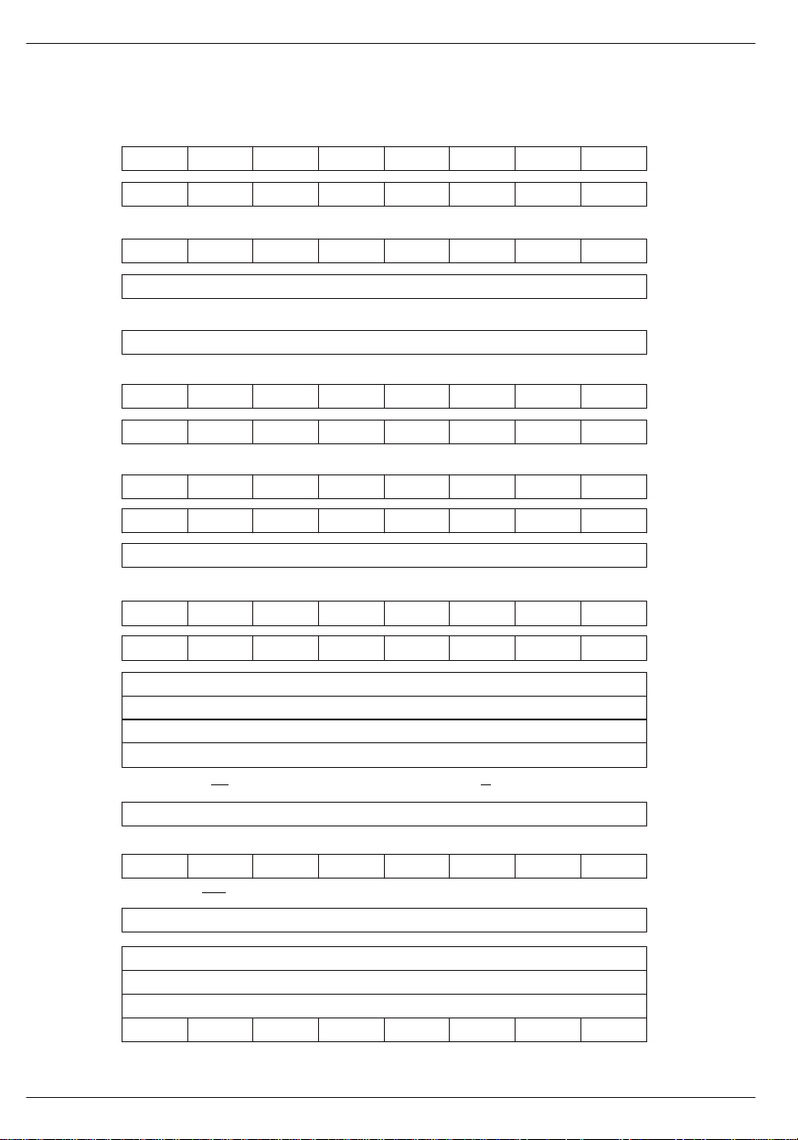
DS5000 SERIES SPECIAL FUNCTION REGISTER MAP Figure 4–12
DIRECT BYTE
ADDRESS
0F0H
(MSB)
F7 F6 F5 F4 F3 F2 F1 F0
BIT ADDRESS
USER’S GUIDE
SPECIAL FUNCTION
REGISTER SYMBOL
(LSB)
B
0E0H
0D0H
0C7H
0C6H
0B8H
0B0H
0A8H
0A0H
99H
98H
90H
8DH
8CH
8BH
8AH
E7 E6 E5 E4 E3 E2 E1 E0
C AC F0 RS1 RS0 OV P
D7 D6 D5 D4 D3 D2 D1 D0
NOT BIT ADDRESSABLE
PA3 PA2 PA1 PA0 RA32/8 ECE2
NOT BIT ADDRESSABLE
RWT PS PT1 PX1 PT0 PX0
BF – – BC BB BA B9 B8
B7 B6 B5 B4 B3 B2 B1 B0
EA ES ET1 EX1 ET0 EX0
AF – – AC AB AA A9 A8
A7 A6 A5 A4 A3 A2 A1 A0
NOT BIT ADDRESSABLE
SM0 SM1 SM2 REN TB8 RB8 TI RI
9F 9E 9D 9C 9B 9A 99 98
97 96 95 94 93 92 91 90
NOT BIT ADDRESSABLE
NOT BIT ADDRESSABLE
NOT BIT ADDRESSABLE
NOT BIT ADDRESSABLE
PAA
SL
ACC
PSW
TA
MCON
IP
P3
IE
P2
SBUF
SCON
P1
TH1
TH0
TL1
TL0
GATE C/T M1 M0 GATE C/T M1 M0
89H
TF1 TR1 TF0 TR0 IE1 IT1 IE0 IT0
88H
87H
83H
82H
81H
80H
* BITS IN ITALICS ARE NONVOLATILE
8F 8E 8D 8C 8B 8A 89 88
SMOD POR
87 86 85 84 83 82 81 80
NOT BIT ADDRESSABLE
PFW
WTR
NOT BIT ADDRESSABLE
NOT BIT ADDRESSABLE
NOT BIT ADDRESSABLE
NOT BIT ADDRESSABLE
29
EPFW
EWT
TMOD
TCON
STOP IDL
PCON
DPH
DPL
SP
P0
050396 28/173
Page 30
USER’S GUIDE
DS5001/DS5002 SERIES SPECIAL FUNCTION REGISTER MAP Figure 4–13
DIRECT BYTE
ADDRESS
(MSB) (LSB)BIT ADDRESS
0F0H
F7 F6 F5 F4 F3 F2 F1 F0
SPECIAL FUNCTION
REGISTER SYMBOL
B
0E0H
0DAH
0D8H RPCTL
0D0H PSW
0B8H IP
0B0H P3
0A8H IE
0A0H P2
98H SCON
E7 E6 E5 E4 E3 E2 E1 E0
ST7 ST6 ST5 ST4 IA0 F0 IBF 0BF
RNR ––– EXBS AE IBI DMA RPC
DF DE DD DC DB DA D9 D8
C AC F0 RS1 RS0 OV P
D7 D6 D5 D4 D3 D2 D1 D0
PA3 PA2 PA1 PA0 RG1
RNGE3 RNGE2 RNGE1 RNGE0 ––– –––
RWT PS PT1 PX1 PT0 PX0
BF ––– ––– BC BB BA B9 B8
B7 B6 B5 B4 B3 B2 B1 B0
EA ES ET1 EX1 ET0 EX0
AF ––– ––– AC AB AA A9 A8
A7 A6 A5 A4 A3 A2 A1 A0
SM0 SM1 SM2 REN TB8 RB8 TI RI
9F 9E 9D 9C 9B 9A 99 98
NOT BIT ADDRESSABLE
NOT BIT ADDRESSABLE0CFH RNR
NOT BIT ADDRESSABLE0C7H TA
NOT BIT ADDRESSABLE0C6H MCON
PES
NOT BIT ADDRESSABLE0C3H CRC HIGH
NOT BIT ADDRESSABLE0C2H CRC LOW
PM SL
MDM CRC
NOT BIT ADDRESSABLE0C1H CRC
NOT BIT ADDRESSABLE99H SBUF
RG0
ACC
RPS
90H P1
89H TMOD
88H TCON
81H SP
80H P0/DBB
* BITS IN ITALICS ARE NONVOLATILE
050396 29/173
97 96 95 94 93 92 91 90
GATE M1 M0 GATE M1 M0
TF1 TR1 TF0 TR0 IE1 IT1 IE0 IT0
8F 8E 8D 8C 8B 8A 89 88
SMOD PFW EPFW
D7 D6 D5 D4 D3 D2 D1 D0
87 86 85 84 83 82 81 80
POR
NOT BIT ADDRESSABLE8DH TH1
NOT BIT ADDRESSABLE8CH TH0
NOT BIT ADDRESSABLE8BH TL1
NOT BIT ADDRESSABLE8AH TL0
C/TC/TC/T
NOT BIT ADDRESSABLE
WTR
NOT BIT ADDRESSABLE87H PCON
NOT BIT ADDRESSABLE83H DPH
NOT BIT ADDRESSABLE82H DPL
NOT BIT ADDRESSABLE
EWT
STOP IDL
30
Page 31

USER’S GUIDE
POWER CONTROL REGISTER
Label: PCON Register Address: 087H
D7 D6 D5 D4 D3 D2 D1 D0
SMOD POR PFW WTR EPFW EWT STOP IDL
Bit Description:
PCON.7 SMOD
“Double Baud Rate”: When set to a 1, the baud rate is doubled when the serial port is being used
in modes 1, 2, or 3.
Initialization: Cleared to a 0 on any reset.
Read Access: Can be read normally at any time.
Write Access: Can be written normally at any time.
PCON.6 POR
“Power On Reset”: Indicates that the previous reset was initiated during a Power On sequence.
Initialization: Cleared to a 0 when Power On Reset occurs. Remains at 0 until it is set to a 1
by software.
Read Access: Can be read normally at any time.
Write Access: Can be written only by using the Timed Access Register.
PCON.5: PFW
“Power Fail Warning”: Indicates that a potential power failure is in progress. Set to 1 whenever V
voltage is below the V
threshold. Cleared to a 0 immediately following a
PFW
CC
read operation of the PCON register. Once set, it will remain set until the
read operation occurs regardless of activity on VCC. After PFW is cleared by
< V
a read, it will return to a 1 if V
CC
PFW
.
Initialization: Cleared to a 0 during a Power On Reset.
Read Access: Can be read normally anytime.
Write Access: Not writable.
PCON.4: WTR
“Watchdog Timer Reset”: Set to a 1 following a Watchdog Timer timeout. If Watchdog T imer Reset is
enabled, this will indicate the cause of the reset. Cleared to 0 immediately
following a read of the PCON register.
Initialization: Set to a 1 after a Watchdog Timeout Reset. Cleared to a 0 on a Power On
Reset. Remains unchanged during other types of resets.
Read Access: May be read normally anytime.
Write Access: Cannot by written.
31
050396 30/173
Page 32

USER’S GUIDE
PCON.3: EPFW
“Enable Power Fail Interrupt”: Used to enable or disable the Power Fail Interrupt. When EPFW is set to a 1,
it will be enabled; it will be disabled when EPFW is cleared to a 0.
Initialization: Cleared to a 0 on any type of reset.
Read Access: Can be read normally anytime.
Write Access: Can be written normally anytime.
PCON.2: EWT
“Enable Watchdog Timer”: Used to enabled or disable the Watchdog Timeout Reset. The Watchdog
Timer is enabled if EWT is set to a 1 and will be disabled if EWT is cleared
to a 0.
Initialization: Cleared to a 0 on a No–V
Power on Reset. Remains unchanged during
LI
other types of reset.
Read Access: May be read normally anytime.
Write Access: Can be written only by using the Timed Access register.
PCON.1: STOP
“Stop”: Used to invoke the Stop mode. When set to a 1, program execution will ter-
minate immediately and Stop mode operation will commence. Cleared to a 0
when program execution resumes following a hardware reset.
Initialization: Cleared to a 0 on any type of reset.
Read Access: Can be read anytime.
Write Access: Can be written only by using the Timed Access register.
PCON.0: IDL
“Idle” Used to invoke the Idle mode. When set to a 1, program execution will be
halted and will resume when the idle bit is cleared to 0 following an interrupt
or a hardware reset.
Initialization: Cleared to 0 on any type of reset or interrupt.
Read Access: Can be read normally anytime.
Write Access: Can be written normally anytime.
050396 31/173
32
Page 33

USER’S GUIDE
TIMER CONTROL REGISTER
Label: TCON Register Address 088H
D7 D6 D5 D4 D3 D2 D1 D0
TF1 TR1 TF0 TR0 IE1 IT1 IE0 IT0
Bit Description:
TCON.7: TF1
“Timer 1 Overflow Flag”: Status bit set to 1 when Timer 1 overflows from a previous count value of all
1’s. Cleared to 0 when CPU vectors to Timer 1 interrupt service routine.
Initialization: Cleared to 0 on any type of reset.
TCON.6: TR1
“Timer 1 Run Control”: When set to a 1 by software, Timer 1 operation will be enabled.
Timer 1 is disabled when cleared to 0.
Initialization: Cleared to 0 on any type of reset.
TCON.5: TF0
“Timer 0 Overflow”: Status bit set to 1 when Timer 0 overflows from a previous count value of all
1’s. Cleared to 0 when CPU vectors to Timer 0 interrupt service routine.
Initialization: Cleared to 0 on any type of reset.
TCON.4: TR0
“Timer 0 Run Control”: When set to a 1 by software, Timer 0 operation is enabled. Timer 0 is dis-
abled when cleared to 0.
Initialization: Cleared to 0 on any type of reset.
TCON.3: IE1
“Interrupt 1 Edge Detect”: Set to 1 to signal when a 1–to–0 transition (IT=1) or a low level (IT=0) has
been detected on the INT1
pin. Cleared to a 0 by hardware when interrupt
processed only if IT1=1.
Initialization: Cleared to 0 on any type of reset.
TCON.2: IT1
“Interrupt 1 Type Select”: When set to 1, 1–to–0 transitions on INT1
will be used to generate interrupt
requests from this pin. When cleared to 0, INT1 is level-activated.
Initialization: Cleared to a 0 on any type of reset.
TCON.1: IE0
“Interrupt 0 Edge Detect”: Set to a 1 to signal when a 1–to–0 transition (IT0=1) or a low level (IT0=0)
has been detected on the INT0
pin. Cleared to a 0 by hardware when inter-
rupt processed only if IT0=1.
Initialization: Cleared to a 0 on any type of reset.
33
050396 32/173
Page 34

USER’S GUIDE
TCON.0: IT0
“Interrupt 0 Type Select”: When set to 1, 1–to–0 transitions on INT0 will be used to generate interrupt
requests from this pin. When cleared to 0, INT0
is level–activated.
Initialization: Cleared to a 0 on any type of reset.
TIMER MODE REGISTER
Label: TMOD Register Address: 089H
D7 D6 D5 D4 D3 D2 D1 D0
GATE C/T M1 M0 GATE C/T M1 M0
Bit Description:
TMOD.7 (Timer 1);
TMOD.3 (Timer 0): GATE
“Gate Control”: When set to 1 with TRn=1, timer/counter’s input count pulses will only be
delivered while a 1 is present on the INT
pulses will always be received by the timer/counter a long as TRn=1.
Initialization: Cleared to 0 on any reset.
TMOD.6 (Timer 1);
TMOD.2 (Timer 0) C/T
“Counter/Timer Select”: When set to 1, the counter function is selected for the associated timer;
when cleared to 0, the timer function is selected.
Initialization: Cleared to 0 on any reset.
pin. When cleared to 0, count
TMOD.5, TMOD.4 (Timer 1);
TMOD.1, TMOD.0 (Timer 0): M1,M0
“Mode Select”: These bits select the operating mode of the associated timer/counter as fol-
lows:
M1 M0
0 0 Mode 0: 8 bits with 5–bit prescale
0 1 Mode 1: 16 bits with no prescale
1 0 Mode 2: 8 bits with auto–reload
1 1 Mode 3: Timer 0 – Two 8–bit timers
Timer 1 – Stopped
Initialization: Cleared to 0 on any reset.
050396 33/173
34
Page 35

USER’S GUIDE
SERIAL CONTROL REGISTER
Label:SCON Register Address: 098H
D7 D6 D5 D4 D3 D2 D1 D0
SM0 SM1 SM2 REN TB8 RB8 TI RI
Bit Description:
SCON.7, SCON.6: SM0, SM1
“Mode Select”: Used to select the operational mode of the serial I/O port as follows:
SM0 SM1 MODE WORD FUNCTION BAUD LENGTH CLOCK PERIOD
0 0 Mode 0 SYNC 8–bits 12 t
0 1 Mode 1 ASYNC 10–bits Timer 1 Overflow
1 0 Mode 2 ASYNC 11–bits 64 t
1 1 Mode 3 ASYNC 11–bits Timer 1 Overflow
Initialization: Cleared to 0 on any type of reset.
SCON.5: SM2
“Multiple MCU Comm”: Used to enable the multiple microcontroller communications feature for
modes 2 and 3. When SM2=1, RI will be activated only when serial words
are received which cause RB8 to be set to a 1.
Initialization: Cleared to a 0 on any type of reset.
CLK
CLK
or 32 t
CLK
SCON.4: REN
“Receive Enable”: When set to 1, the receive shift register will be enabled. Disabled when
cleared to 0.
Initialization: Cleared to a 0 on any type of reset.
SCON.3: TB8
“Xmit Bit 8”: Can be set or cleared to define the state of the 9th data bit in modes 2 and 3 of
a serial data word.
Initialization: Cleared to a 0 on any type of reset.
SCON.2: RB8
“Rec. Bit 8”: Indicates the state of the 9th data bit received while in modes, 2 or 3. If mode
1 is selected with SM2=0, RB8 is the state of the stop bit which was received.
RB8 is not used in mode 0.
Initialization: Cleared to a 0 on any type of reset.
SCON.1: TI
“Xmit Interrupt”: Status bit used to signal that a data word has been completely shifted out. In
mode 0, it is set at the end of the 8th data bit. Set when the stop bit is transmitted in all other modes.
35
050396 34/173
Page 36

USER’S GUIDE
Initialization: Cleared to a 0 on any type of reset.
SCON.0: RI
“Receive Interrupt”: Status bit used to signal that a serial data word has been received and
loaded into the receive buffer register . In mode 0, it is set at the end of the 8th
bit time. It is set at the mid–bit time of the incoming stop bit in all other modes
of a valid received word according to the state of SM2.
INTERRUPT ENABLE REGISTER
Label:IE Register Address: 0A8H
D7 D6 D5 D4 D3 D2 D1 D0
EA
– – ES ET1 EX1 ET0 EX0
Bit Description:
IE.7: EA
“Enable All Interrupts”: When set to 1, each interrupt except for PFW may be individually enabled or
disabled by setting or clearing the associated IE.x bit. When cleared to 0,
interrupts are globally disabled and no pending interrupt request will be ac-
knowledged except for PFW.
IE.4: ES
“Enable Serial Interrupt”: When set to 1, an interrupt request from either the serial port’s TI or RI flags
can be acknowledged. Serial I/O interrupts are disabled when cleared to 0.
IE.3: ET1
“Enable Timer 1 Interrupt”: When set to 1, an interrupt request from Timer 1’s TF1 flag can be acknowl-
edged. Interrupts are disabled from this source when cleared to 0.
IE.2: EX1
“Enable External Interrupt 1”: When set to 1, an interrupt request from the IE1 flag can be acknowledged.
Interrupts are disabled from this source when cleared to 0.
IE.1: ET0
“Enable Timer 0 Interrupt”: When set to 1, an interrupt request from Timer 0’ s TF0 flag can be acknowl-
edged. Interrupts are disabled from this source when cleared to 0.
IE.0: EX0
“Enable External Interrupt 0”: When set to 1, an interrupt from the IE0 flag can be acknowledged. Inter-
rupts are disabled from this source when cleared to 0.
050396 35/173
36
Page 37

USER’S GUIDE
INTERRUPT PRIORITY REGISTER
Label:IP Register Address: 0B8H
D7 D6 D5 D4 D3 D2 D1 D0
RWT – – PS PT1 PX1 PT0 PX0
Bit Description:
IP.7: RWT
“Reset Watchdog Timer”: When set to a 1, the Watchdog Timer count will be reset and counting will
begin again. The RWT bit will then automatically be cleared again to 0. Writ-
ing a 0 into this bit has no effect.
Initialization: Cleared to a 0 on any reset.
Read Access: Cannot be read.
Write Access: Can be written only by using the Timed Access register.
All of the following bits are read/write at any time and are cleared to 0 following any hardware reset.
IP.4: PS
“Serial Port Priority”: Programs Serial Port interrupts for high priority when set to 1. Low priority is
selected when cleared to 0.
IP.3: PT1
“Timer 1 Priority”: Programs Timer 1 interrupt for high priority when set to 1. Low priority is se-
lected when cleared to 0.
IP.2: PX1
“Ext. Int. 1 Priority”: Programs External Interrupt 1 for high priority when set to 1. Low priority is
selected when cleared to 0.
IP.1: PT0
“Timer 0 Priority”: Programs Timer 0 Interrupt for high priority when set to 1. Low priority is se-
lected when cleared to 0.
IP.0: PX0
“Ext. Int. 0 Priority” Programs External Interrupt 0 for high priority when set to 1. Low priority is
selected when cleared to 0.
37
050396 36/173
Page 38

USER’S GUIDE
DS5001 CRC REGISTER
Label: CRC Register Address: 0C1H
RNGE3 RNGE2 RNGE1 RNGE0 ––– ––– MDM CRC
Bit Description:
CRC.7–4 RNGE3–0
Initialization: Reset to 0 on a No V
Read Access: Can be read at any time.
Write Access: Cannot be written by the application software. Can only be written via the
Determines the range over which a power–up CRC will be performed.
Addresses are specified on 4K boundaries.
reset.
LI
Bootstrap Loader.
CRC.1 MDM
When set to 1, the bootstrap loader will attempt to use a modem (UART) on
PE4 if CRC is incorrect. This feature is no longer useful following the
obsoletion of the corresponding modem devices.
Initialization: Reset to 0 on a No V
reset.
LI
Read Access: Can be read at any time.
Write Access: Cannot be written by the application software. Can only be written during
Program Load mode.
CRC.0 CRC
When set to 1, a CRC check will be performed on power–up or watchdog
timeout. CRC will be checked against stored values. An error will initiate
Program Load mode. This bit will not be present in the DS5002FP as the
device does not support the power–on CRC function.
Initialization: Reset to 0 on a No V
reset.
LI
Read Access: Can be read at any time.
Write Access: Cannot be written by the application software. Can only be written during
Program Load mode.
050396 37/173
38
Page 39

USER’S GUIDE
DS5000 MEMORY CONTROL REGISTER
Label:MCON Register Address: 0C6H
D7 D6 D5 D4 D3 D2 D1 D0
PA3 PA2 PA1 PA0 RA32/8 ECE2 PAA SL
Bit Description:
MCON.7–4: PA3–0
“Partition Address”: Used to select the starting address of Data Memory on the Byte–wide bus.
Program space lies below the partition address.
PA3 PA2 PA1 PA0 Partition Address
0 0 0 0 0000H
0 0 0 1 0800H
0 0 1 0 1000H
0 0 1 1 1800H
0 1 0 0 2000H
0 1 0 1 2800H
0 1 1 0 3000H
0 1 1 1 3800H
1 0 0 0 4000H
1 0 0 1 4800H
1 0 1 0 5000H
1 0 1 1 5800H
1 1 0 0 6000H
1 1 0 1 6800H
1 1 1 0 7000H*
1 1 1 1 8000H*
*A 4K byte increment (not 2K bytes) in the Partition Address takes place between bit field values 11 10B and
11 1B.
Initialization: Set to all 1’s on a No V
Power On Reset or when the Security Lock bit is
LI
cleared to a 0 from previous 1 state. These bits are also set to all 1’s when
any attempt is made to have them cleared to all 0’s with the SL bit set to 1
(illegal condition).
Read Access: May be read anytime.
Write Access: PAA bit must = 1 in order to write PA3–0. Timed Access is not required to
write to PA3–0 once PAA=1.
MCON.3: RA32/8
“Range Address”: Set the maximum usable address in on the Byte–wide bus.
RA32/8=0 sets Range Address = 1FFFH (8K)
RA32/8=1 sets Range Address = 7FFFH (32K)
Initialization: Set to a 1 during a No V
Power On Reset and when the Security Lock bit
LI
(SL) is cleared to a 0 from a previous 1 state. Remains unchanged on all oth-
er types of resets.
39
050396 38/173
Page 40

USER’S GUIDE
Read Access: May be read normally anytime.
Write Access: Cannot be modified by the application software; can only be written via the
Bootstrap Loader.
MCON.2: ECE2
“Enable Chip Enable 2”: Used to enable or disable the CE2
signal for the Byte–wide bus data
memory. This bit should always be cleared to 0 in the DS5000, DS5000-32,
DS2250–8 and DS2250–32 versions.
Initialization: Cleared to 0 only during a No V
Power On Reset.
LI
Read Access: Read normally anytime.
Write Access: Can be written normally at any time.
MCON.1: PAA
“Partition Address Access”: Used to protect the programming of the Partition Address select bits. PA3–0
cannot be written when PAA=0. PAA can be written only via the Timed Access register.
Initialization: PAA is cleared on any reset.
Read Access: PAA may be read anytime.
Write Access: The Timed Access register must be used to perform any type of write opera-
tion on the PAA bit.
MCON.0: SL
“Security Lock”: Indicates that the security lock is set when SL=1.
Initialization: Cleared to a 0 on a no V
power on reset.
LI
Read Access: Read normally any time.
Write Access: Can only be modified by the Lock and Unlock commands of the Bootstrap
loader. This bit cannot be modified by the application software or by the
Bootstrap loader Write command.
DS5001 MCON REGISTER
Label: MCON Register Address: 0C6H
PA3 PA2 PA1 PA0 RG1 PES PM SL
Bit Description:
MCON.7–4: PA3–0
Initialization: Unaffected by watchdog, external, or power–up resets. Set to 1111B on a
Read Access: Can be read normally at any time.
Partition Address. When PM=0, this address specifies the boundary
between program and data memory in a continuous space.
reset.
No V
LI
050396 39/173
40
Page 41

USER’S GUIDE
Write Access: Timed Access Protected. Cannot be written by the application software if
set to 0000B by the serial loader. If a 0000B is written via the serial loader
and the security lock is set, the Partition will become 111 1B. The same will
occur if write access is available and application software writes a 0000B. In
addition, these bits will be set to 1111B if security lock is cleared.
MCON.3: RG1
One of two bits that determine the range of program space. RG0 is located
in the RPCTL register.
Initialization: Unaffected by watchdog, external, or power–up resets. Set to 1 on a No V
reset or a clearing of the security lock.
Read Access: Can be read at any time.
Write Access: Cannot be modified by the application software. Can only be written via the
Bootstrap Loader.
MCON.2: PES
Peripheral Enable Select. When this bit is set, the data space is controlled
by PE1–PE4. Peripherals are memory–mapped in 16K blocks, and are
accessed by MOVX instructions on the Byte–wide bus.
Initialization: Cleared by all resets.
Read Access: Can be read at any time.
Write Access: Can be written at any time.
MCON.1: PM
Partition Mode. When PM=0, a partitionable, continuous memory map is
invoked. When PM=1, one of four fixed allocations is used.
Initialization: Unaffected by watchdog, external, or power–up resets. Cleared on a No V
reset.
Read Access: Can be read at any time.
Write Access: Cannot be modified by the application software. Can only be modified via
the Boostrap Loader.
LI
LI
MCON.0: SL
“Security Lock”: Indicates that the security lock is set when SL=1.
Initialization: Cleared to a 0 on a no V
power on reset.
LI
Read Access: Read normally any time.
Write Access: Can only be modified by the Lock and Unlock commands of the Bootstrap
loader. This bit cannot be modified by the application software or by the
Bootstrap loader Write command.
41
050396 40/173
Page 42

USER’S GUIDE
PROGRAM STATUS WORD REGISTER
Label:PSW Register Address: 0D0H
D7 D6 D5 D4 D3 D2 D1 D0
C AC F0 RS1 RS0 OV P
All of the bits in PSW except parity are read/write and are cleared to 0 on any type of reset. The Parity bit is read only
and is cleared to 0 on any type of reset.
Bit Description:
PSW.7: C
“Carry”: Set when the previous operation resulted in a carry (during addition) or a
borrow (during subtraction). Otherwise cleared.
PSW.6: AC
“Auxiliary-Carry”: Set when the previous operation resulted in a carry (during addition) or a
borrow (during subtraction) from the low–order nibble. Otherwise cleared.
PSW.5: F0
“User Flag 0”: General–purpose flag bit which can be set or cleared as needed.
PSW.4–3: R1–R0
“Register Bank Select”: Used to select an 8–byte bank of registers within the Data Register space to
be assigned as R0–R8 in subsequent instructions. The 8–byte bank starting
address selection is as follows:
R1 R0 Data Register Address (R0)
0 0 00H
0 1 08H
1 0 10H
1 1 18H
PSW.2: OV
“Overflow”: Set when a carry was generated into the high–order bit but not a carry out of
the high–order bit as a result of the previous operation, and visa–versa. OV
is normally used in 2’s complement arithmetic.
PSW.0: P
“Parity”: Set if the modulo–2 sum of the eight bits of the accumulator is 1 (odd parity);
cleared on even parity.
050396 41/173
42
Page 43

USER’S GUIDE
DS5001/DS5002 RPC CONTROL REGISTER
Label: RPCTL Register Address: 0D8H
RNR ––– EXBS AE IBI DMA RPCON RG0
Bit Description:
RPCTL.7 RNR
Initialization: Cleared after all resets. Bit will be set approximately 160 µsec after a reset.
Read Access: Can be read at any time.
Write Access: Cannot be written.
When internal hardware sets this read–only bit to a 1, a new value may be
read from the random number generator register of the DS5001/DS5002
(RNR;0CFh). This bit is cleared when the random number is read, and
approximately 160 µs are required to generated the next number.
RPCTL.5 EXBS
The Expanded Bus Select routes data memory access (MOVX) to the
expanded bus formed by ports 0 and 2 when set.
Initialization: Cleared after all resets.
Read Access: Can be read at any time.
Write Access: Can be written at any time.
RPCTL.4 AE
Access Enable is used when a software reload is desired without using the
Bootstrap Loader. When set, the device will be temporarily configured in a
Partitionable configuration with the Partition at 4K. This will occur even if the
PM=1. When cleared, the prior memory configuration is resumed.
Initialization: Cleared after all resets.
Read Access: Can be read at any time.
Write Access: Can be written at any time, Timed Access protected.
RPCTL.3 IBI
When using the RPC mode, an interrupt may be required for the Input
Buffer Flag. This interrupt is enabled by setting the Input Buffer Interrupt
(IBI) bit. At this time, the timer 1 interrupt is disabled, and this RPC mode
interrupt is used in its place (vector location 1BH). This bit can be set only
when the RPCON bit is set.
Initialization: Cleared on all resets, and when the RPCON bit is cleared.
Read Access: Can be read at any time.
Write Access: Can be written when the RPC mode is enabled (RPCON=1).
RPCTL.2 DMA
This bit is set to enable DMA transfers when RPC mode is invoked. It can
only be set when RPCON=1.
Initialization: Cleared on all resets, and when RPC is cleared.
43
050396 42/173
Page 44

USER’S GUIDE
Read Access: Can be read anytime.
Write Access: Can be written when the RPC mode is enabled (RPCON=1).
RPCTL.1 RPCON
Enable the RPC 8042 I/O protocol. When set, port 0 becomes the data bus,
and port 2 becomes the control signals.
Initialization: Cleared on all resets.
Read Access: Can be read at any time.
Write Access: Can be written at any time.
RPCTL.0 RG0
This is a Range bit which is used to determine the size of the program
memory space. Its usage is shown above.
Initialization: Unaffected by watchdog, external, or power–up resets. Cleared on a No V
reset or clearing of the security lock.
Read Access: Can be read at any time.
Write Access: Cannot be modified by the application software. Can only be modified via
the Bootstrap loader.
DS5001/DS5002 RPC STATUS REGISTER
Label: RPS Register Address: 0DAH
ST7 ST6 ST5 ST4 IA0 F0 IBF OBF
Bit Description:
RPS.7–4: General purpose status bits that can be written by the microcontroller and
can be read by the external host.
Initialization: Cleared when RPCON=0.
Read Access: Can be read by DS5001/DS5002 and host CPU when RPC mode is invoked.
Write Access: Can be written by the DS5001/DS5002 when RPC mode is invoked.
LI
RPS.3: IA0
Stores the value of the external system A0 for the last DBBIN Write when
a valid write occurs (as determined by the IBF flag).
Initialization: Cleared when RPC=0.
Read Access: Can be read by DS5001/DS5002 and host CPU when in RPC mode.
Write Access: Automatically written when a valid DBBIN Write occurs. Cannot be written
otherwise.
RPS.2: F0
General purpose flag written by the DS5001/DS5002 and read by the
external host.
Initialization: Cleared when RPC=0.
050396 43/173
44
Page 45

Read Access: Can be read by DS5001/DS5002 and host CPU when in RPC mode.
Write Access: Can be written by the DS5001/DS5002 when in RPC mode.
USER’S GUIDE
RPS.1: IBF
Input Buffer Full Flag is set following a write by the external host, and is
cleared following a read of the DBBIN by the DS5001/DS5002.
Initialization: Cleared when RPC=0.
Read Access: Can be read by DS5001/DS5002 and host CPU when in RPC mode.
Write Access: Written automatically as part of the RPC communication. Cannot be set by
the application software.
RPS.0: OBF
Output Buffer Full Flag is set following a write of the DBBOUT by the
DS5001/DS5002, and is cleared following a read of the DBBOUT by the
external host.
Initialization: Cleared when RPC=0.
Read Access: Can be read by DS5001/DS5002 and host CPU when in RPC mode.
Write Access: Written automatically as part of the RPC communication. Cannot be set by
the application software.
45
050396 44/173
Page 46

USER’S GUIDE
INSTRUCTION SET
Introduction
The Secure Microcontroller executes an instruction set
which is object code compatible with the industry standard 8051 microcontroller. As a result, software tools
written for the 8051 are compatible with the Secure
Microcontroller, including cross–assemblers, compilers, and debugging tools.
There are a total of 42 instruction types recognized by
the Secure Microcontroller. When the instruction uses
both source and destination operands, they are specified in the order of “destination, source”.
Addressing Modes
There are eight addressing modes. Five of these are
used to address operands. The other three are used in
instructions which transfer execution of the program to
another address (e.g., Branch, Jump, Call).
The modes which address source operands, include
Register Addressing, Direct Addressing, Register–Indirect Addressing, Immediate Addressing and RegisterIndirect with Displacement. The first three of these can
also be used to address a destination operand. Most
instructions use operands that are located in the Internal
Data Registers.
The addressing modes used for the Control Transfer
instructions include Relative Addressing, Page Addressing, and Extended Addressing.
The operation of these addressing modes is summarized below, followed by an example.
Register Addressing
Register Addressing is used on operands contained in
one of the eight registers (R7–R0) of the currently selected Working Register Bank. A register bank is selected via a 2–bit field in the PSW Special Function register. All of the Working registers may also be accessed
through either Direct Addressing or Register-Indirect
Addressing as well. This is due to the fact that the Working registers are mapped into the lower 32 bytes of Internal Data RAM as discussed above.
ADD A, R4 ; Add Accumulator to Working
; register R4
Direct Addressing
Direct Addressing is the only mode available for use on
operands within the Special Function registers. Addressing of bytes may also be used to access the 128
Internal Data registers.
MOV 072H, 074H ; Load direct register (addr. 072H)
; with direct register (074H)
Direct addressing of bits is available on 128 bits located
in the Internal Data registers in byte addresses of 20H –
2FH inclusive. Direct bit addressing is also available in
Special Function registers located at addresses on
8–byte boundaries starting at 80H (i.e., 80H, 88H, 90H,
98H, ...0F0H, 0F8H).
SETB 00H ; Set addressable bit 00H (D0 in
; Internal Data Reg. 20H)
Register Indirect Addressing
Some instructions use Register–Indirect Addressing for
accessing operands in other Internal Data registers.
This is done by using the contents of Working register
R1 or R0 as a pointer to other Internal Data registers.
ANL A, @R0 ; Logical AND of Accumulator with
; Internal Data register; pointed to
; by contents of R0
In addition, this addressing is used via the Stack Pointer
register (SP) for manipulation of the stack. The stack
area is contained in the Internal Data Register area. The
PUSH and POP instructions are the only ones which
use SP for this addressing mode.
PUSH P0 ; Save the contents of the Port 0
; SFR latch on the stack
The R0, R1, and the DPTR registers are used with Register–Indirect Addressing for accessing Data Memory.
R1 or R0 in the selected Working Register bank may be
used for accessing location within a 256–byte block
pointed to by the current contents of the P2 SFR latch
(address high byte).
MOVX A, @R1 ; Load the Accumulator with the
; contents of Data Memory
; addressed by the 8–bit contents
; of R1
050396 45/173
46
Page 47

USER’S GUIDE
The 16–bit DPTR register may be used to access any
Data Memory location within the 64K byte space.
MOVX @DPTR,A ; Load the Data Memory location
; pointed to by the contents of the
; DPTR register with the contents
; of the Accumulator.
Immediate Addressing
Immediate Addressing is used to access constants for
use as operands which are contained in the current
instruction in Program Memory .
ORL A, #040H ; Logical OR of the Accumulator
; with the constant value of 040H
Register–Indirect with Displacement
Register–Indirect with Displacement Addressing is
used to access data in look–up tables in Program
Memory space. The location accessed is pointed to by
the contents of either the DPTR or the PC registers,
which are used as a base register added together with
the contents of the Accumulator (A), which is used as an
index register.
MOVC A, @DPTR+A ; Load the Accumulator with
; the contents of the Program
; Memory location pointed to
; by the value of the DPTR
; register plus the value
; contained in the Accumulator
Relative Addressing
Relative Addressing is used in the determination of a
destination address for the Conditional Branch instructions. Each of these instructions includes an 8–bit byte
which contains a 2’s complement address offset (–127
to +128) which is added to the PC to determine the destination address which will be branched to when the
tested condition is found to be true. The PC points to the
Program Memory location immediately after the Branch
instruction when the offset is added. If the condition is
found to be not true, then program execution continues
from the address of the following instruction.
JZ –20 ; Branch to the location (PC+2) –
20 ; if the contents of the Accumulator
; = 0
Page Addressing
Page Addressing is used by the Control Transfer
instructions to specify a destination address within the
2K byte block in which the next contiguous instruction
resides. The full 16–bit address is calculated by taking
the highest-order five bits for the next contiguous
instruction (PC+2) and concatenating them with the
lowest-order 11–bit filed contained in the current
instruction. 11–bit field provides an efficient instruction
encoding of a destination address for these instructions.
0830 ACALL 100H ; Call to the subroutine at
; address 0100H + current
; page address
In this case the destination address would be 800H +
100H or 900H.
Extended Addressing
Extended Addressing is used in the Control Transfer
Instructions to specify a 16–bit destination address
within the entire 64K byte addressable range of the
Secure Microcontroller.
LJMP 0FF80H ; Jump to address 0FF80H
47
050396 46/173
Page 48

USER’S GUIDE
Program Status Flags
All of the Program Status flags are contained in the PSW
register. Instructions which affect the states of the flags
are summarized below.
INSTRUCTIONS THAT AFFECT FLAG SETTINGS
FLAGS
INSTRUCTION
C OV AC INSTRUCTION
ADD CLR C 0
ADDC CPL C
SUBB ANL C, bit
MUL 0 ANL C, bit
DIV 0 ORL C, bit
DA ORL C, bit
RRC MOV C, bit
RLC CJNE
SETB C 1
LEGEND:
0 = Cleared to 0
1 = Set to a 1
= Modified according to the result of the operation.
FLAGS
COVAC
050396 47/173
48
Page 49

USER’S GUIDE
PART
SECTION 5: MEMORY INTERCONNECT
The Secure Microcontroller family is divided between
chips and modules. This sections illustrates the
memory interconnect for the various chips and shows
block diagrams of selected modules. The Soft Microprocessor chips are 80–pin QFP packages that connect to
low power CMOS SRAM. The SRAM connection is
made through the Byte–wide bus. When using a chip,
the user must connect this Byte–wide bus to the RAM as
shown in this section. In module form, the bus is connected inside the package. Table 5–1 shows some of
the preferred RAM choices. Note that any standard
SRAM will work, but data retention lifetime is dependent
on RAM data retention current and battery capacity.
Lower currents naturally allow the use of smaller batteries. This is covered in detail in Section 6.
RECOMMENDED SRAMs FOR USE WITH SOFT MICROCONTROLLERS Table 5–1
DATA RETEN-
TION CURRENT
RAM SIZE VENDOR
NUMBER
25°C 40°C 70°C
8K x 8 Dallas DS2064 0.05 µA – –
8K x 8 Sharp LH5168 – – 0.6 µA
32K x 8 Hitachi HM62256LP–SL – 3 µA 10 µA
32K x 8 Mitsubishi M5M5256BP–LL 1 µA – 10 µA
32K x 8 Sony CXK58257AP–LX 1 µA 2 µA 10 µA
32K x 8 Sony CXK58527AP–LLX 0.3 µA 0.6 µA 3 µA
128K x 8 Hitachi HM628128LP–SL 1 µA – 10 µA
128K x 8 Mitsubishi M5M51008P–LL 1 µA – 10 µA
128K x 8 Sony CXK581000P–LL 1.2 µA 2.4 µA 12 µA
DATA RETEN-
TION CURRENT
DATA RETEN-
TION CURRENT
Recommended RAMs are given with the manufacturers specified data retention current at 3V . Missing numbers are conditions unspecified by the manufacturer.
In the case of the DS5000FP, the microprocessor can
connect to either one or two SRAMs. They can be 8K bytes or 32K bytes, though the case of two 8K RAMs is unlikely from a cost perspective. Figure 5–1 illustrates the
memory connection of a DS5000FP connected to one
32K x 8. CE1
the WE
using CE2
provides the chip select, and R/W supplies
signal. A second RAM could be added by simply
as the chip enable with a common connec-
tion for the other signals.
In the case of DS5000 based modules including
DS5000(T) and DS2250T, the SRAM is connected as
described above. Connections running between the micro chip and RAM are not available at the pins. The
DS2250–64 has a second SRAM on CE2
. The timekeeping versions also have the real–time clock connected to CE2
. A block diagram in Figure 5–2 shows the
module configuration with 32K RAM and a real–time
clock. This is identical for DS2250 or DS5000 modules.
These are functionally identical and only differ in form
factor.
49
050396 48/173
Page 50

USER’S GUIDE
ÇÇ
ÇÇ
MEMORY INTERCONNECT OF THE DS5000FP Figure 5–1
DS5000FP
+5v
+3v
13
V
CC
54
V
LI
PORT0
V
BA14–BA0
CCO
R/W
CE1
12
10
74
32K x 8 SRAM
28
V
CC
27
WE
20
CS
22
OE
A14–A0
PORT1
BD7–BD0
PORT2
73
EA
PORT3
52
GND
CE2
+5v
78
DS5000 SERIES MODULE BLOCK DIAGRAM Figure 5–2
DS5000(T), DS2250(T)
40–PINS
V
V
CC
(8)
PORT0
(8)
PORT1
(8)
PORT2
(8)
PORT3
CCO
ADDR
DATA
CE1
D7–D0
14
GND
32K X 8 SRAMDS5000FP
REAL TIME CLOCK
(OPTION)
050396 49/173
ALE
PSEN
EA
RST
XTAL1
XTAL2
GND
CE2
VLI
+3V
50
Page 51

USER’S GUIDE
The DS5001FP has several memory options. It can be
connected to between one 8K byte SRAM and four
32K byte SRAMs. It will also support one 128K byte
SRAM. In most cases the DS5001FP is used for its
greater memory access so it will not be used with 8K
RAMs. In the Partitionable mode (see Section 4), the
DS5001FP can be connected to one or two SRAMs.
Figure 5–3 illustrates the connection of two 32K x 8
SRAMs. Each RAM has its own chip enable, with a common WE
generated by the DS5001FP R/W signal.
When using the DS5001FP with only one RAM, the second chip enable will simply remain unconnected. This
solution provides a total of 64K bytes of memory which
the user can partitions into program and data segments.
The Partition setting has no impact on the interconnect.
In the non–partitionable case, the DS5001FP can be
connected to three or four 32K x 8 SRAMs. The four
RAM case is shown in Figure 5–4. Each RAM has its
own chip enable. To use three RAMs, simply omit the
unused chip enable (CE2 or 4) as described in Section
4. In other ways, this hardware configuration is similar to
the Partitionable mode discussed above. While this
provides the full 128K bytes of memory, it requires more
space and cost than the version shown in Figure 5–5.
This uses the 128K byte SRAM. All program and data
memory is contained within the single chip. The DS5001
manages the addressing and decoding. Note the MSEL
signal is connected to ground to initiate this mode. The
PM bit and Range must still be configured by the user
during program loading.
Using the Partition, the microcontroller determines which
memory blocks are program and write protects the appropriate addresses.
MEMORY INTERCONNECT OF THE PARTITIONABLE DS5001/DS5002 Figure 5–3
+5V
+3V
DS5001FP/DS5002FP
13
V
CC
54
V
LI
PORT0
V
CCO
R/W
CE1
BA14–BA0
12
10
74
28
27
20
V
CC
WE
CS
A14–A0
32K x 8 SRAM
OE
22
PORT1
PORT2
PORT3
52
GND
BD7–BD0
MSEL
CE2
+5V
14
2
D7–D0
14
GND
32K x 8
SRAM
VCC
28
V
CC
WE
27
WE
CS
20
CS
A14–A0
A14–A0
D7–D0
D7–D0
14
GND
GND
32K x 8
SRAM
22
OE
OE
050396 50/173
51
Page 52

USER’S GUIDE
MEMORY INTERCONNECT OF THE NON–PARTITIONABLE DS5001FP, DS5002FP Figure 5–4
+5V
+3V
DS5001FP/DS5002FP
13
VCC
54
VLI
PORT0
V
CCO
R/W
CE1
BA14–BA0
12
10
74
28
27
20
V
CC
WE
CS
A14–A0
32K X 8
SRAM
OE
22
PORT1
PORT2
PORT3
52
GND
MSEL
14
BD7–BD0
CE2
CE3
CE4
+5V
D7–D0
GND
2
63
62
14
32K X 8
SRAM
28
V
CC
27
WE
20
CS
A14–A0
D7–D0
14
GND
32K X 8
SRAM
28
V
CC
27
WE
20
CS
A14–A0
D7–D0
GND
14
OE
OE
22
22
050396 51/173
52
32K X 8
SRAM
28
VCC
27
WE
20
CS
A14–A0
D7–D0
GND
14
OE
22
Page 53

MEMORY INTERCONNECT USING THE 128K SRAM Figure 5–5
DS5001FP/DS5002FP
+5v
+3v
13
V
CC
54
V
LI
PORT0
PORT1
BA14–BA0
PORT2
BD7–BD0
PORT3
52
GND
V
CCO
R/W
CE1
CE2
CE3
MSEL
12
10
74
2
63
14
USER’S GUIDE
128K x 8
SRAM
28
V
CC
27
WE
20
CS1
2
A16
31
A15
A14–A0
D7–D0
16
GND
CS2
OE
30
22
In the 128K x 8 configuration, the microprocessor converts the CE3
into A15 and CE2 into A16. Grounding the
MSEL pin causes this configuration. The physical location of program memory will be between addresses
00000 to 0FFFFh. Data memory will be located between
10000h and 1FFFFh. These physical locations are
transparent to the user. From a software perspective,
both program and data are located between 0000 and
FFFFh. When the MSEL pin is grounded, the device
cannot be partitioned. The MSL bit accessed through
the bootstrap loader is used to select access to the
64KB data or 64KB program segment via the loader in
the 128K x 8 configuration.
The Soft Microcontroller line has two modules based on
the DS5001 series. The DS2251T 128K Micro Stik uses
a DS5001FP . The DS2252T Secure Micro Stik is based
on the DS5002FP. All computing features are derived
from the DS5001. The DS5002 device provides
memory security features in addition. The modules are
available in 32K, 64K, and 128K byte versions. Two example block diagrams are shown below.
Figure 5–6 is a block diagram of the DS2251T with 128K
bytes of NV RAM. This part can also be built with 32K or
64K bytes. In this case, the 128K RAM is replaced with
one or two 32K byte RAMs. Figure 5–7 shows a
DS2252T with 32K bytes of RAM. This part is also available in 64K or 128K byte versions. For 64K, two RAMs
are used. For 128K, the single 128K SRAM is used. This
is entirely transparent to the user and is provided for
completeness.
050396 52/173
53
Page 54

USER’S GUIDE
DS2251T–128 BLOCK DIAGRAM Figure 5–6
DS2251T
72 PINS
DS5001FP 128K X 8 SRAM
V
V
(8)
(8)
(8)
(8)
CC
PORT0
PORT1
PORT2
PORT3
ALE
RST
PSEN
PROG
PF
VRST
PE3
PE4
XTAL1
XTAL2
GND
CCO
ADDR
R/W
DATA
CE1
DS1283
REAL TIME CLOCK
PE1
V
LI
050396 53/173
(14)
(8)
R/W
INTA
INTB
INTP
SQW
+3V
BYTE–WIDE ADDRESS BUS
BYTE–WIDE DATA BUS
54
Page 55

DS2252T–32 BLOCK DIAGRAM Figure 5–7
Ç
Ç
Ç
Ç
DS2252T
USER’S GUIDE
40 PINS
DS5002FP 32K X 8 SRAM
V
V
(8)
CC
PORT0
(8)
PORT1
(8)
CCO
ADDR
DATA
CE1
PORT2
(8)
PORT3
REAL TIME CLOCK
ALE
RST
XTAL1
XTAL2
PROG
PE1
SDI
GND
V
LI
+3V
55
050396 54/173
Page 56

USER’S GUIDE
SECTION 6: LITHIUM/BATTERY BACKUP
Soft Microcontroller devices are lithium backed for data
retention in the absence of V
. In the Soft Microcon-
CC
troller the state of the microcontroller is also maintained,
unlike a conventional processor system using an external NV RAM. This section is a comprehensive discussion of the lithium back up feature. It covers system
design, battery attach procedure, I/O pin restrictions,
lifetime calculations, and battery/RAM size tradeoffs.
Some of the information is unnecessary to module
users but will provide background information for proper
handling and system design. Each section will highlight
both chip and module considerations when there are differences.
When properly used, lithium backed microcontrollers
provide better than 10 years of data retention in the
absence of power. This means that a total of over 10
years in the absence of power at room temperature is
guaranteed. Elevated temperatures cause higher than
normal data retention current to be drawn by a RAM.
However, these remarks are only relevant to a system
that is powered down. While +5V is applied to the
device, the lithium cell is isolated from any loading.
Therefore, data retention must be viewed in the context
of the power supply duty cycle. For example, if a system
is rated for 10 years of data retention, but will have
power applied for 12 hours per day, the expected lifetime is greater than 20 years.
DATA RETENTION
The Secure Microcontroller family provides nonvolatile
storage in ordinary SRAM. It accomplishes this by battery–backing the memory in the absence of power.
When power (V
ates an internal power–fail reset condition as discussed
in the next chapter. At this time, SRAM chip enables are
taken to a logic high inactive state. Also, I/O port pins
also go to a logic high state. If power continues to fall and
crosses below the lithium threshold, the microprocessor
enters the data retention state, and power is drawn from
the lithium cell. The power supply output to the SRAM
) is switched from VCC to the lithium cell. VCC is
(V
CCO
subsequently ignored, except for comparators that
monitor its level. Lithium backed chip enables are main-
) begins to fail, the processor gener-
CC
tained at a logic high state with lithium power, but non–
backed chip enables follow V
down. Individual prod-
CC
uct differences should be observed. Maintaining chip
enables at an inactive level and lowering the power supply to approximately +3V causes the NV RAM to enter a
data retention state. Thus the combination retains data
for a long period as the circuits draw a very small current
from the lithium cell. Modules easily attain better than
10 years of data retention. Chip solutions can be
designed to achieve a much greater lifetime depending
on the user’s needs.
BATTERY BACKED CIRCUITS
The Secure Microcontroller is the only computer that is
completely lithium backed. This means that both internal configuration and data are preserved when power is
removed. However, unlike a simple NV RAM, the microprocessor is an extremely complex circuit that must be
fully prepared for lithium backup. Once prepared, the
microprocessor is guaranteed to draw less than 75 nA
from its backup source. This number is typically 5 nA.
The user’s selection of RAM will determine the total
loading on the lithium cell. In the case of a module, Dallas has screened the RAM to make certain that the total
loading guarantees better than 10 years of data retention for the selected lithium cell at room temperature.
In order to achieve this ultra–low power state, special
logic in the microprocessor places all internal nodes in a
predictable (low power) state. This occurs during system power down while VCC is falling below the reset voltage threshold and is still above the lithium voltage. If the
power supply slews between these threshold voltages
faster than 40 µs (130 µs for DS5001/2), the circuits may
not complete the backup procedure and the microprocessor backup current could be substantially greater
than 75 nA, and/or program/data corruption could occur.
Fortunately , a modest amount of system capacitance is
enough to prevent fast slewing. The actual value will
depend on the total system loading. This slew rate must
be met for either a chip or module solution. In either
case, the microprocessor must have time to prepare for
lithium backup. Figure 6–1 illustrates the power supply
conditions that should be met.
050396 55/173
56
Page 57

POWER SUPPLY SLEW RATE Figure 6–1
40 µs, 130 µs
V
CC
V
CCMIN
V
LI
LITHIUM
CURRENT
USER’S GUIDE
Each time VCC is restored, the lithium backed functions
will remain as they were left. A result is that many of
these values are not altered on a reset condition except
for the ‘no battery reset’. In the documentation, this is
referred to as ‘No V
reset’. This will occur after the first
LI
time VCC is applied to the microprocessor. The ‘no battery reset’ state is documented in the section on resets.
A module user will never see the ‘no battery reset’ condition as it was cleared during assembly and test prior to
leaving the factory .
BATTERY ATTACH PROCEDURE
This section applies to microprocessor chips only, not
modules. When a microprocessor is received from the
factory, it is completely uninitialized. All nonvolatile functions are absent since there is no backup source connected to the chip. As mentioned above, the microprocessor must place circuits in a low power state to
prepare for lithium backup. If a battery were attached to
an uninitialized chip, the backup current would be
unpredictable. For this reason, the following battery
attach procedure must be followed.
1. Apply V
2. Attach the lithium cell to the V
3. Configure and program the device as normal.
(Optional at this time.)
4. Power down the microprocessor (remove V
using the guidelines discussed above while leaving
the battery attached.
to the microprocessor.
CC
input.
LI
CC
The first time a battery is attached to the microprocessor
is a special event. When power is applied in the absence
of a lithium cell, the device performs a No V
This allows the microprocessor to initialize control bits
that are ordinarily nonvolatile and unaffected by a reset.
The microprocessor will never be completely in this
state again unless all power (including battery) is
removed by the user. In order to provide the extremely
low back up currents (<75 nA), the circuits must configure themselves for lithium backup. This is done when
is removed from the chip. That is, the microproces-
V
CC
sor IS NOT CONFIGURED FOR LITHIUM BACKUP
when it is received. Therefore, the battery should be
attached with V
at +5V . This will prevent the micropro-
CC
cessor from placing a load on the lithium cell until VCC is
removed. At this time, the microprocessor performs its
power down procedure and prepares for ultra low power
data retention. Attaching the battery to an unpowered
microprocessor places an unknown load on the lithium
cell. This may drain the cell excessively and should not
be done.
BATTERY LIFETIME
The calculations of data retention lifetime are helpful for
chip or module users. They can serve as design and
system reliability guidelines. All lithium backed microcontroller modules are rated for better than 10 years of
data retention in the absence of V
)
these guidelines, similar performance can be achieved
using chips. It is also not difficult to achieve better than
at 25°C. Following
CC
Reset.
LI
57
050396 56/173
Page 58

USER’S GUIDE
10 years depending on the user’s actual environment
and design goals.
The system lifetime can be determined from three
parameters: 1) Data retention current, 2) Lithium cell
capacity, 3) Lithium self–discharge. Current production
lithium cells have extremely good self–discharge performance. Manufacturer’s data and Dallas Semiconductor characterization has determined that the self–
discharge of a coin cell lithium battery is less than 0.5%
per year at 25°C. Consequently , even after 15 years of
shelf life, the lithium cell would have 90% of its capacity
remaining. Therefore when using a lithium coin cell, the
self–discharge mechanism is not a consideration for
rating equipment life.
Data retention current is a combination of RAM, microprocessor, Real–time clock (RTC), and other lithium
Battery capacity in amp hours
Data retention current in amps * # days in a year * # of hours in a day
As an example, the Microprocessor rated for 75 nA,
SRAM for 500 nA, RTC for 400 nA for a total of 950 nA.
–3
120 * 10
(75 + 500 + 400) * 10–9 * 24 * 365) 8.54 * 10
backed circuits, if any. In a Dallas module, these are
screened for combination with the appropriate battery.
In using a chip, the user must balance the size/cost of a
larger lithium cell with the data retention current/cost of
SRAMs.
When designing a chip–based system and selecting the
appropriate SRAM, the important specification is data
retention current. This is not the same as standby current. Data retention current should be specified with
CE = VIH and VCC=3V. This specification is usually
available at 25°C, and possibly for other temperatures.
Selected RAMs have been provided in chapter 5 with
the manufacturer specified data retention current. The
lifetime calculations are illustrated below. The formula
for data retention life in years is as follows:
A Panasonic CR1632 lithium cell is used with a capacity
of 120 mAh.
–3
120 * 10
= = 14 years
–3
Thus a system with less than 1 µA of data retention current and a CR1632 lithium cell will achieve well over 10
years of data retention in the absence of VCC. Referring
to the recommended RAM chart in the previous section,
the user will find a variety of RAMs that allow this at room
temperature. It makes no difference if the system operates at 70°C, as long as data retention is at 25°C. If storage is at elevated temperature, than the data retention
current should be derated accordingly. If the manufacturer does not specify data retention current over temperature, a conservative number is a 70% increase per
10°C. Thus if a RAM in data retention mode draws 1 µA
at 25°C, it will draw approximately 1.7 µA at 35°C.
180 * 10
–3
(2400 + 75) * 10–9 * 24 * 365) 21.68 * 10
Note that these ratings are for continuous data retention
is assumed absent for the entire period. Actual
so V
CC
050396 57/173
A second example illustrates the case of elevated temperature storage.
In this example, the system is constructed using a
DS5001FP chip with a Sony CXK581000P–LL 128K x 8
SRAM. The system will be stored at 40°C. As shown in
the table in chapter 5, the data retention current of this
RAM is 2.4 µA at 40°C. The DS5001FP data retention
current will actually drop as temperature increases, so
the maximum of 75 nA is conservative. This gives a total
data retention current of 2475 nA. In this system, a
Rayovac BR2325 with a capacity of 180 mAh is used.
–3
180 * 10
= = 8.3 years
–3
performance have a longer lifetime based on the ratio of
time when VCC is applied vs. data retention time.
58
Page 59

USER’S GUIDE
LITHIUM BATTERY USAGE
In the vast majority of applications, lithium batteries provide a reliable means of backing up data and configuration. The voltage varies only slightly over its useful life,
so it is difficult to measure capacity . A CR chemistry will
begin life at 3.3V and drop to 2.9V near the end of life.
As a consequence, some users choose to incorporate
battery clips so that lithium cells are easily replaced.
This is not recommended since such clips are susceptible to shock and vibration. It is possible that the connection to a lithium cell would be momentarily lost during
such a shock, resulting in a potential loss of data. Therefore, soldered battery tabs are recommended. If a user
elects to use a battery clip with a capacitor (to support
momentary disconnect), the leakage of the capacitor
should be considered in the lifetime calculations.
FRESHNESS SEAL
The Secure Microcontroller family is designed to maximize the lifetime of a lithium backup source. The circuits
described above contribute to a long life. There is one
further provision that will benefit users that intend to
store their systems in an unpowered state, but that do
not require it to retain data during this period. An example might be a completed system stored in inventory.
Since data retention is not required, there is no benefit to
using even the modest lithium current that will normally
be drawn. For this reason, Secure Microcontrollers
incorporate the Freshness Seal. The Freshness Seal
electrically isolates the lithium cell from any external
loading. Thus even in the absence of power, the SRAM
and Real–Time Clock leakage currents will not be
drawn from the lithium cell for as long as the Freshness
Seal is applied.
This feature is available to module users of the DS5000
series [DS5000(T), DS2250T] and all users of the
DS5001/2 series [DS5001FP, DS5002FP, DS2251T,
DS2252T]. In the case of DS5000 and DS2250 modules, the factory ships these with the Freshness Seal
applied. In the case of a DS5001, DS5002 series
device, the Freshness Seal can be applied via the Bootstrap Loader at any time. Thus if the Freshness Seal is
not removed, the time that a Secure Microcontroller
based system is stored in inventory will not reduce the
data retention lifetime since the lithium cell is unloaded.
To clear the Freshness Seal, simply apply V
CC
. On a
DS5000 series device, the Freshness Seal can not be
restored by the user. Therefore, if Freshness Seal is
desired for storage, the part should not be powered up
when received or installed. Since a DS5001/DS5002
series device can invoke the Freshness Seal via the
Loader, this restriction does not apply. To invoke the
Freshness Seal on a DS5001, DS5002 series device,
the “N” command should be issued to the Bootstrap
Loader.
IMPORTANT APPLICATION NOTE
The pins on a Secure Microcontroller chip or module are generally as resilient as other CMOS circuits. They have no
unusual susceptibility to electrostatic discharge (ESD) or other electrical transients. However, no pin on a Soft
Microcontroller chip or module should ever be taken to a voltage below ground. Negative voltages on any pin
can turn on internal parasitic diodes that draw current directly from the battery. If a device pin is connected to the
“outside world” where it may be handled or come in contact with electrical noise, protection should be added to prevent the device pin from going below –0.3V . It is also common for power supplies to give a small undershoot on power
up, which should be prevented. Application Note 93, Design Guidelines for Microcontrollers Incorporating NV RAM,
discusses how to protect devices against these conditions.
59
050396 58/173
Page 60

USER’S GUIDE
SECTION 7: POWER MANAGEMENT
Introduction
All Dallas Semiconductor microcontrollers are implemented using fully static CMOS circuitry for low power
consumption. Power consumption is a linear function of
crystal frequency. Two software initiated modes are
available for further power saving at times when processing is not required and V
is at normal operating volt-
CC
age. These are the Idle and Stop modes. The additional
third mode is the Data Retention or Zero Power State
which is made possible by the on–chip, circuitry. The
control and status bits which apply to these operating
modes are contained in the PCON register and are summarized in Figure 7–1. In addition, Table 7–1 summarizes the state of external pins in each of these modes.
Idle Mode
The Idle mode suspends activity of the CPU. However,
the on–chip I/O function, including the timer/counters,
and serial port continue their operation. This greatly reduces the number of switching nodes and thereby dramatically reduces the total power consumption of the
device. The Idle mode is useful for applications in which
lower power consumption is desired with fast response
to external interrupts but no other processing.
Software can invoke the Idle mode by setting the IDL bit
in the PCON register (PCON.0) to a logic 1 as shown in
Figure 7–1. The instruction which sets this bit will be the
last instruction executed before Idle mode operation begins. Once in the Idle mode, the microprocessor preserves the entire CPU status including the Stack Pointer, Program Counter, Program Status Word,
Accumulator, and RAM. There are two ways to terminate the Idle mode. The first is from an interrupt which
has been previously enabled prior to entering Idle
mode. This will clear the IDL bit in the PCON register
and will cause the CPU to enter the interrupt service routine as normal. When the RETI instruction is executed,
the next instruction which will be executed is the one
which immediately follows the instruction that set the
IDL bit.
The second method of terminating the Idle mode is by a
Reset. At this time the IDL bit is cleared and the CPU is
placed in the reset state. Since the clock oscillator continues to run in the Idle mode, an oscillator start up delay
(referred to as t
in the AC Electrical Specifications)
POR
will not be generated following the reset. Two machine
cycles are required to complete the reset operation (24
oscillator periods). It should be noted that the Watchdog
Timer continues to run during Idle and that a reset from
the on–chip Watchdog Timer will terminate Idle mode.
CONTROL/STATUS BITS FOR POWER CONTROL Figure 7–1
Bit Description:
PCON.6: POR
“Power On Reset” Indicates that the previous reset was initiated during a Power On sequence.
Initialization: Cleared to a 0 when a Power On Reset occurs. Remains at 0 until it is set to a
1 by software.
Read Access: Can be read normally at any time.
Write Access: Can be written only by using the Timed Access register.
PCON.5: PFW
“Power Fail Warning” Indicates that a potential power failure is in progress. Set to a 1 when V
voltage is below the V
threshold. Cleared to a 0 immediately following a
PFW
read of the PCON register. Once set, it will remain set until read regardless
of VCC.
Initialization: Cleared to a 0 during a Power–On Reset.
Read Access: Can be read normally at any time.
050396 59/173
60
CC
Page 61

USER’S GUIDE
Write Access: Cannot be written.
PCON.3: EPFW
“Enable Power Fail
Interrupt”: Used to enable or disable the Power Fail Interrupt. When EPFW is set to a 1,
it will be enabled; it will be disabled when EPFW is cleared to a 0.
Initialization: Cleared to a 0 on any type of reset.
Read Access: Can be read normally anytime.
Write Access: Can be written normally anytime.
PCON.1: STOP
“Stop”: Used to invoke the Stop mode. When set to a 1, program execution will ter-
minate immediately and Stop mode operation will commence. Cleared to a 0
when program execution resumes following a hardware reset.
Initialization: Clear to a 0 on any type of reset.
Read Access: Can be read anytime.
Write Access: Can be written only by using the Timed Access register.
PCON.0: IDL
“Idle”: Used to invoke to Idle mode. When set at a 1, program execution will be
halted and will resume when the Idle bit is cleared to 0 following an interrupt
or a hardware reset.
Initialization: Cleared to 0 on any type of reset or interrupt.
Read Access: Can be read normally anytime.
Write Access: Can be written normally anytime.
PIN STATES IN IDLE/STOP MODES Table 7–1
MODE
Idle Byte–wide 1 1 Port Data Port Data Port Data Port Data
Idle Expanded 1 1 Hi–Z Port Data Address Port Data
Stop Byte–wide 1 0 Port Data Port Data Port Data Port Data
Stop Expanded 1 0 Hi–Z Port Data Port Data Port Data
Stop Mode
The Stop mode is initiated by setting the STOP bit in the
PCON register (PCON.1). The operation of the oscillator is halted in the Stop mode so that no internal clocking
signals are produced for either the CPU or the I/O circuitry. An External Reset via the RST pin is the only
means of exiting this mode without powering down (V
taken below V
PROGRAM
MEMORY
) and then back up to produce a
CCmin
ALE PSEN P0 P1 P2 P3
Power On Reset. The STOP bit may only be set by using
the Timed Access software procedure described in Section 8. Since the oscillator is disabled in this mode, the
Watchdog Timer will cease operation. When the external reset signal is issued to terminate the Stop mode, a
21,504 clock delay will be generated to allow the clock
oscillator to start up and its frequency to stabilize as is
CC
done for a Power On Reset as described in Section 10.
61
050396 60/173
Page 62

USER’S GUIDE
The original contents of those Special Function registers that are initialized by a reset are lost.
power fail condition so that the operational state of the
processor can be saved just prior to entering the Data
Retention.
Voltage Monitoring Circuitry
The on–chip voltage monitoring circuitry automatically
places the microprocessor in its Data Retention state in
the absence of V
control signals are generated and that power from the
lithium cell is applied at the proper times so that the Program/Data RAM, data in the Scratchpad Registers and
certain Special Function Registers remain unchanged
when V
is cycled on and off. In addition, an interrupt is
CC
available for signaling the processor of an impending
. It insures that the proper internal
CC
The voltage monitoring circuitry recognizes three voltage thresholds below nominal operating voltage. These
thresholds are identified as V
voltage), V
(minimum operating voltage), and V
CCmin
(lithium supply) voltage. These thresholds are used to
initiate required actions within the microprocessor during situations when VCC power is cycled on and off. The
timing diagram shown in Figure 7–2 illustrates key internal activities during power cycling.
SECURE MICROCONTROLLER POWER CYCLING TIMING Figure 7–2
V
CC
V
PFW
V
CCMIN
V
LI
t
F
INTERRUPT
SERVICE
ROUTINE
t
CSU
(Power Fail Warning
PFW
LI
050396 61/173
CLOCK
OSC.
INTERNAL
RESET
LITHIUM
CURRENT
62
t
POR
Page 63

USER’S GUIDE
Power Fail Interrupt
When VCC is stable, program execution proceeds as
normal. If V
voltage and drop to a level below the V
should decay from its nominal operating
CC
threshold,
PFW
then the internal PFW status flag (PCON.5) will be set.
In addition, a Power Fail Warning interrupt will be generated if it has been enabled via the EPFW control bit
(PCON.3). The purpose of these indicators is to warn
the processor of a potential power failure.
The V
value for VCC (V
V
PFW
threshold is above the specified minimum
PFW
) for full processor operation. The
CCmin
threshold is selected so that with a reasonable
power supply slew rate, ample time is allowed for the application software to save all critical information which
would otherwise be lost in the absence of VCC. Such information may include the states of the Accumulator,
Stack Pointer, Data Pointer , and other Special Function
registers which are initialized with a reset when V
CC
voltage is applied once again. Saved data can be
placed into Scratchpad RAM or Byte–wide NV RAM.
Through the use of the Power Fail Warning interrupt, an
orderly shutdown of the system may be performed prior
to the time that processor operation is halted in the
event that V
The PFW flag is set to a logic 1 whenever the V
is below the V
voltage is removed entirely.
CC
threshold. It is cleared in one of two
PFW
CC
level
ways: 1) a read of the PFW bit from software, or 2) a
Power On Reset. If VCC is still below the V
PFW
threshold
when the bit is cleared, then the PFW bit will be immediately set once again. An interrupt will be generated any
time that both the EPFW bit and the PFW flag are set.
Total Power Failure
If VCC voltage should fall below the V
processor operation will halt. This is done by first placing
the CPU in a reset condition and then stopping the internal clock oscillator circuit, as illustrated in Figure 7–2. At
this time the interface to the Program/Data RAM is disabled by pulling the CE
line high. This action guarantees
an orderly shutdown for the lithium-backed RAM.
The microprocessor is automatically placed in the Data
Retention state, if V
voltage drops below VLI, the con-
CC
trol circuitry accomplishes this by switching the internal
power supply line (V
) from pin to the lithium power
CCI
source. At this time, data is retained and no power is
drawn from VCC.
CCmin
threshold,
When power is once again applied to the system, the
V
voltage will eventually cross the VLI threshold.
CC
When this action is detected, the microprocessor will
automatically switch its internal supply line from the lithium source back to the V
eventually goes above the V
pin. When VCC voltage
CC
threshold, the clock
CCmin
oscillator is allowed to start up and an internal Power On
Reset cycle is executed. Part of the cycle involves a
considerable delay that is generated to allow the clock
oscillator frequency to stabilize. Activity on the RST pin
is ignored until this sequence is completed. The time required for this cycle is shown as t
in Figure 7–2 and
POR
is specified in the AC Electrical Specifications. A detailed description of the Power On reset cycle operation
is given in Section 10.
Typically, the time taken for the Power On Reset cycle
will be longer to complete than it takes for V
above the V
threshold. In this case the internal PFW
PFW
CC
to rise
flag will be reset before execution of the user’s program
begins as illustrated in Figure 7–2. If the Power On Reset cycle completes before V
CC>VPFW
be set again as a result of VCC<V
, then PFW will
during user soft-
PFW
ware execution. A Power Fail Interrupt will occur at this
time if the EPFW bit is enabled. A user should monitor
the POR bit to know the power supply status. Refer to
Figure 7–3 for details.
Partial Power Failures
Two cases of partial power failure can occur in which
VCC voltage does not go through a completed power fail
cycle as described above. The first case is that in which
drops below the V
V
CC
to its nominal level without going below the VLI threshold. The second case is that in which VCC drops below
the V
threshold and then returns to its nominal level
PFW
without going below the V
cases are very possible in a system application and
could be caused by a “brownout” condition on an AC
power line.
The first case is indistinguishable by the software from
the complete power fail cycle which was previously described. When V
drops below V
CC
be set and the clock oscillator will be stopped when V
drops below V
CCmin
that if VCC never drops below the VLI threshold, the internal power supply line will never be switched over to
the lithium cell. When VCC rises back above the V
threshold and then returns
CCmin
threshold. Both of these
CCmin
the PFW flag will
PFW
CC
. The only operational difference is
CCmin
63
050396 62/173
Page 64

USER’S GUIDE
threshold, the Power On Reset cycle will be executed as
before. As a result, no special processing is required in
then it will remain cleared until the next time V
below V
PFW
.
software to accommodate this case.
As long as the PFW flag is set, an interrupt condition is
In the case that V
dips without going below VLI, the
CC
PFW flag will be set and a Power Fail Warning interrupt
will still occur when VCC drops below the V
PFW
threshold. The PFW flag will remain set until it is cleared by either a reset of the flag by the software or by a Power On
cycle. If it is cleared while V
is still below the V
CC
PFW
threshold, it will be immediately set again. If it is cleared
after VCC has risen back above the V
PFW
threshold,
defined if EPFW is set. If the software executes a service routine in response to a PFW interrupt and exits the
service routine with the PFW flag still set, then the processor will be immediately interrupted again. In a typical
application, however, the Power Fail Interrupt service
routine would test the PFW flag in a conditional loop to
determine if V
has risen back above V
CC
then return control to the main program in response to
the event. See Figure 7–3 for details.
SECURE MICROCONTROLLER POWER MANAGEMENT Figure 7–3
RESET VECTOR
POWER–FAIL W ARNING
INTERRUPT VECTOR
POR = 0?
YES
SET POR
NO
RUN NORMAL
RESET ROUTINE
POWER HAS FALLEN BELOW VPFW,
CLEAR PFW FLAG BY READING
(READ PCON)
SAVE CRITICAL DATA TO NVRAM;
PREPARE FOR POWER FAILURE
PFW
goes
CC
and would
LONG POWER–UP
SLEW RATE, KEEP
050396 63/173
PFW = 1?
YES
CHECKING
NO
SET EPFW
POWER–FAIL
INTERRUPT
POWER ON
BOOT ROUTINE
64
PFW = 1?
YES
VOLTAGE IS STILL BELOW
VPFW, NOT SAFE TO RUN
NO
POWER HAS
RETURNED,
RESUME
OPERATION
Page 65

USER’S GUIDE
SECTION 8: SOFTWARE CONTROL
Introduction
Several features have been incorporated into the
Secure Microcontroller to help insure the orderly execution of the application software in the face of harsh electrical environments. Any microcontroller which is operating in a particularly noisy environment is susceptible
to loss of software control. Electrical transients such as
a glitch on the clock or a noise spike on an I/O pin can
cause software problems like the loss of key variables in
internal registers and/or execution of code out of its logical sequence. Such transients can send the microcontroller into an indefinite period of seemingly random software execution.
Timed Access, Watchdog Timer and CRC hardware
features have been built in to help provide control and
recovery under difficult operating conditions. The op eration of these features is described below.
Timed Access
The Timed Access feature is provided to help insure
controlled access by software to critical configuration
bits in the Special Function registers. These protected
bits may only be written through the execution of a specific multiple instruction software sequence which involves the Timed Access register . This restriction is designed to help prevent a potentially catastrophic change
in the configuration by an inadvertent write during times
when software control has been lost.
Access register at location 0C7h. The first write should
be a value of 0AAh and the second should be a value of
55H. After this sequence is performed, the protected
bits may be modified. Upon receiving a 0AAH in the
Timed Access register , two timers are initiated. The first
timer allows two instruction cycles to write a 55H. This
means a one– or two–cycle instruction may be used. If
55H is not written within two cycles, Timed Access is reset. The second timer requires that the protected bit be
modified within four instruction cycles. Since this timer
started prior to writing 55H, the remaining time depends
on which type of instruction was used to write 55H. If a
one–cycle instruction was used to write 55H, then three
cycles remain to modify protected bits. In the same way,
if a two–cycle instruction was used to write 55H, then
two cycles remain. This is depicted in Figure 8–1. The
following code sequences demonstrate this procedure.
In the rare case that back to back Timed Accesses are
performed, the user must be aware that the four–cycle
Timed Access window must close before another T imed
Access can begin. This is only an issue if a one–cycle
instruction is performed after the MOV TA, #55h instruction, leaving one cycle remaining in the four–cycle
count. The user can eliminate this problem by either
using a two–cycle instruction after the MOV TA, #55h
instruction, or by inserting one other instruction between
the two Timed Access procedures. Violation this rule
will result in a failure of the second Timed Access procedure, leaving the bit(s) unmodified.
In order to modify the protected bits listed in T able 8–1, a
pattern of two bytes must first be written to the Timed
TIMED ACCESS Figure 8–1
WRITE
AAh
2 CYCLES
WRITE
55h
4 CYCLES
65
WINDOW FOR
TIMED ACCESS CLOSES
050396 64/173
Page 66

USER’S GUIDE
This code allows the reset of the Watchdog Timer:
MOV 0C7H,#0AAH ; 1st TA Value
MOV 0C7H,#055H ; 2nd TA Value 2 Cycles
SETB IP.7 ; Reset Watchdog Timer 1 Cycle
The Watchdog Timer bit may have been set using ORL IP, #80H which
takes two cycles.
This code allows the reset of the Watchdog Timer using a different approach:
MOV A, #55H ; Setup Acc for fast write
MOV 0C7H, #0AAH ; 1st TA V alue
MOV 0C7H, A ; 2nd TA Value 1 Cycle
MOV A, IP ; Get Current IP 1 Cycle
ORL A, #80H ; Prepare for fast write 1 Cycle
MOV IP, A ; Reset Watchdog Timer 1 Cycle
Note that a new value for IP could have been retrieved from any direct
register instead of the current IP.
The bits which are write access–protected by the Timed Access function are listed in Table 8–1.
TIMED ACCESS PROTECTED CONTROL BITS Table 8–1
BIT NAME MICRO VERSION LOCATION DESCRIPTION
EWT All Secure Micro PCON.2 Enables the Watchdog Timer Reset function
RWT All Secure Micro IP .7 Resets the Watchdog Timer count
STOP All Secure Micro PCON.1 Stop Mode Enable
POR All Secure Micro PCON.6 Power On Reset
PAA DS5000 series MCON.1 Partition Address Access bit (protects PA3–0)
PA3–0 DS5001, DS5002
series
AE DS5001, DS5002
series
MCON.7–4 Partition Address bits
RPCTL.4 Access Enable
The Secure Microcontroller family has a variety of control bits that are critical to the correct operation of the
processor. Several of these are nonvolatile and will not
be altered by a reset. Thus they must be protected from
an accidental write by software that has gone out of control. This is a possibility in all microprocessor based systems, especially those in an industrial environment.
While the Watchdog Timer will recover from this condition, the critical bits must be protected during the interval
before the time–out of the Watchdog T imer.
050396 65/173
The Secure Microcontroller family actually has two levels of protection for these critical bits. The most critical
SFR bits can only be altered using the Bootstrap Loader. An example is the Range function that determines
the total memory. There is no need for an application to
modify this bit during normal operation. For those critical
bits that might need to be modified during normal operation, the Timed Access procedure protects against an
inadvertent write operation.
66
Page 67

USER’S GUIDE
Timed Access provides a statistical protection. It is
unlikely that randomly generated states will correctly
match the sequence and timing required to bypass the
Timed Access logic. Presented below is a brief justification for each bit that is protected by Timed Access.
The EWT bit is protected to prevent errant software from
disabling the Watchdog T imer. The Watchdog is one of
the important mechanisms that assure correct operation and should not be turned off accidentally. RWT is
the bit that software uses to restart the Watchdog time–
out. The Secure Microcontroller makes this more difficult by Timed Access protecting the bit. Thus software
must “really” intend to reset the time–out in order to do
so. Note that the Watchdog Timer is disabled in Stop
mode. Critical applications which rely on the Watchdog
Timer should exercise caution if the application will utilize Stop mode.
POR informs the software of the power supply condition. Specifically, it means the power has previously
dropped below the V
level and returned to nor-
CCMIN
mal. In many systems, this is a unique condition that
requires interaction with external hardware. Protecting
this bit with a Timed Access procedure prevents the
micro from accidentally performing a power on reset
procedure.
On a DS5000 series device, the PAA bit allows software
to alter the Partition. If this is done accidentally, the
resulting configuration could be unrecoverable without
human intervention. This could mean selecting a Partition that is outside of the user’s plan and that causes the
system to fail. In a like manner, the PA3–0 bits on a
DS5001 series device are protected through Timed
Access. As the DS5001 does not have a PAA bit, the
Partition control bits are directly protected. The motivation for protecting the AE bit is similar. This bit invokes a
Partitionable configuration where one had not been
selected during Bootstrap loading. While there are several valid reasons to select AE, accidentally selecting
this condition might be unrecoverable without manual
intervention.
Note that the Timed Access logic protects against the
possibility of a single inadvertent write modifying a critical control bit. It does not protect against inadvertently
entering a section of code that contains the correct
sequence to modify a protected bit. However, the statistical protection does greatly improve the system’s resilience to a crash.
Watchdog Timer
The on–chip Watchdog Timer provides a method of restoring proper operation during transients that cause
the loss of controlled execution of software. When the
Watchdog Timer is enabled, it will eventually reach a
timeout condition after 122,800 machine cycles unless it
is reset by the application software. An internal reset to
the CPU will be generated if the timeout condition is ever
reached. Software which utilizes the Watchdog Timer
must periodically reset the RWT bit so that it will never
be reached during normal operation. The reset operation(s) should be inserted at critical check points in the
program. The Watchdog Timer will monitor program
execution to insure that these check points are reached,
indicating proper operation. If controlled execution of
the software is lost so that these check points are not encountered within the timeout period, then the Watchdog
Timer will provide an automatic reset. A block diagram
of the Watchdog Timer is shown in Figure 8–2.
The Special Function Register bits that are used to control the Watchdog include the Enable Watchdog Timer
bit (EWT; PCON.2), the Reset Watchdog Timer bit
(RWT; IP.7), and the Watchdog Timer Reset status flag
(WTR; PCON.4). The Watchdog Timer incorporates a
free–running counter that starts counting as soon as the
clock oscillator begins operation following a Power On
Reset. If a 12 MHz crystal is used as the time base element, this gives a timeout period of 122.88 ms. The
Watchdog T imer Reset function is enabled with a Timed
Access write operation which sets the EWT bit to a 1. A
Watchdog Timer Reset will then occur the next time that
the free–running counter reaches its timeout condition.
Regardless of whether the Watchdog Timer will be
used, it should be initialized after each reset. If the
Watchdog T imer is desired, then the first step is to reset
the timer count. This is necessary since the timer is free
running and may be about to time–out. Set the RWT bit
to a logic 1 using a Timed Access procedure. This will
restart the timer with the full interval. Then enable the
Watchdog Timer reset function by setting the EWT bit to
a logic 1, again with a Timed Access procedure. Note
that the EWT bit only controls whether the reset is
issued, not whether the timer runs. The Watchdog T imer
must now be reset prior to 122,800 machine cycles or it
will reset the CPU. If the Watchdog Timer is not used,
then clear the EWT bit to a logic 0 using a Timed Access
procedure. Since the EWT bit is nonvolatile, this makes
certain that the Watchdog reset function remains disabled.
67
050396 66/173
Page 68

USER’S GUIDE
During subsequent program execution, the Watchdog
Timer can be reset by a Timed Access write operation
which sets the RWT bit to a 1. This will cause the Watchdog Timer to begin counting machine cycles again from
an initial count of 0. The RWT bit itself is automatically
cleared immediately after the Watchdog Timer is reset.
An instruction sequence which performs this operation
is as follows.
This code allows the reset of the Watchdog Timer:
MOV 0C7H, #0AAH ; 1st TA Value
MOV 0C7H, #055H ; 2nd TA Value
SETB IP.7 ; Reset Watchdog Timer
If the timeout period is ever reached without the timer
being reset by the software, the Watchdog T imer will reset the CPU, set the WTR status flag, and will begin
counting again. The WTR flag allows the application
software to distinguish this type of reset from other possible sources so that special processing can be performed to accommodate this case. This flag will be set in
response to a timeout, regardless of whether the reset is
enabled. The WTR bit is cleared only by a read of the
PCON register. Therefore, this register should be read
during initialization following a reset in order to properly
interpret the source of the reset.
The Watchdog T imer Reset Bit (WTR) is held in a logic 1
state for 8192 clock cycles following the time–out of the
watchdog 122,880 cycle counter. During this time, the
bit may be read but attempts to clear the bit will fail. This
condition will not be noticed if the Enable Watchdog
Timer bit (EWT) is set, because the 8192 cycle count will
be reset during the device reset triggered by the watchdog time–out. The bit may then be cleared, if desired,
during application’s power–on reset routine.
Some applications may use the watchdog timer but not
set the EWT bit, preferring instead to poll the WTR bit in
software to detect a watchdog time–out. In this case,
one approach is for the application software to continually read the EWT bit as long as it is set. When the 8192
clock cycle period is complete, the last read of the EWT
bit will successfully clear the bit and exit the routine.
Alternatively , software can poll the WTR bit until it is set,
then reset the watchdog via the RWT bit to clear the
8192 cycle count. The next read of the PCON register
will clear WTR bit as expected.
The Watchdog Timer is also reset whenever any other
type of reset is issued to the CPU and will begin its count
as soon as the reset condition is released and the application software begins execution.
If operation without the Watchdog Timer is desired, then
the EWT bit should be cleared following any type of
reset by using the Timed Access register. This will
insure that the Watchdog Timer will never cause an
undesired reset during execution of the application software.
WATCHDOG TIMER Figure 8–2
MACHINE CYCLE
050396 67/173
12 CLOCK
COUNTER
122,800 CYCLE COUNTER
RWT
WTR
EWT
68
Page 69

USER’S GUIDE
WATCHDOG TIMER CONTROL BITS
Bit Description:
PCON.4: WTR
“Watchdog Timer Reset” Set to a 1 when a Watchdog Timer timeout occurs. If W atchdog Timer Reset
is enabled, this will indicate the cause of the reset. Cleared to 0 immediately
following a read of the PCON register.
Initialization: Set to a 1 after a Watchdog T imeout. Cleared to a 0 on a No–V
Reset. Remains unchanged during other types of resets.
Read Access: May be read normally anytime.
Write Access: Cannot be written.
PCON.2: EWT
“Enable Watchdog Timer Used to enable or disable the Watchdog Timeout Reset. The Reset is
Reset”: enabled if EWT is set to a 1 and will be disabled if EWT is cleared to a 0. This
bit affects the generation of a reset condition, not the running of the Watch-
dog Timer.
Initialization: Cleared to a 0 on a No–V
Power On Reset. Remains unchanged during
LI
other types of resets.
Read Access: May be read normally anytime.
Write Access: Can be written only by using the Timed Access register.
Power On
LI
IP.7: RWT
“Reset Watchdog Timer”: When set to a 1, the Watchdog Timer count will be reset, and counting will
begin again. The RWT bit will then automatically be cleared again to 0. Writ-
ing a 0 into this bit has no effect. This bit should be set prior to EWT, as the
timers are free–running.
Initialization: Cleared to a 0 on any reset.
Read Access: Cannot be read.
Write Access: Can be written only by using the Timed Access register.
CRC MEMORY VERIFICATION
When using nonvolatile memory, there is always the
potential for a catastrophic event to alter the memory
contents. These events include lightning, massive ESD,
severe mistreatment, etc. No nonvolatile technology is
immune to these events. To compensate, the DS5001
series contains a CRC function that allows for automatic
reset, the microcontroller will automatically perform a
CRC–16 on the memory. The range over which it is performed is selected by the user, and the result is
compared to a pre–stored value. If the CRC–16 is in
error, the DS5001 series microcontroller will enter the
Bootstrap Loader and wait. From the perspective of the
system, the appears held in a reset condition.
verification of memory on power up. The CRC function
is also available to the user for application software use.
Note that this is not available on DS5000 series devices
[DS5000(T), DS2250T, DS5000FP].
T o support this function, the CRC register shown below
is accessible through the Bootstrap Loader. Setting the
CRC bit (LSB) enables the power–up CRC function.
The loader command “W” is used to write to this register.
If the CRC option is selected through the Bootstrap
Loader, then on power up or after a Watchdog Timer
The upper nibble of the CRC register (a hex value
between 0 and F) defines the address space in 4K
050396 68/173
69
Page 70

USER’S GUIDE
blocks over which the CRC calculation is performed.
For example, if the nibble is set to 0001b, the CRC range
is from 0000 to 0FFFh. Once the LSB of the CRC register is set, the loader “I” command will cause the CRC of
the specified block to be computed. The result is automatically stored in the last two bytes of the specified
block. These bytes should not be used by the application. This computation will be correct provided that the
CRC range is less than or equal to the partition if PM=0.
If PM=1, using 32K RAMs, the CRC range must be less
than or equal to the program range.
Watchdog timeout and the CRC check will be performed. If an error is detected, the Bootstrap Loader will
wait for reloading. If there is no error, the application will
begin at address 0000h following a reset. Automatic
checking of the CRC can be disabled by writing a 0 to
the CRC register LSB. As mentioned above, this is
done using the “W” command in loader mode. The CRC
hardware uses registers 0C3h and 0C2h for most and
least significant byte intermediate storage. The
DS5002FP and DS2252T do not perform a CRC check
to ensure software security.
If CRC is enabled, the DS5001FP will automatically
invoke the Bootstrap Loader on either power–up or a
DS5001 CRC REGISTER (Address 0C1h)
RNGE3 RNGE2 RNGE1 RNGE0 ––– ––– MDM CRC
CRC.7–4: RANGE 3–0
Initialization: Reset to 0 on a No V
Read Access: Can be read at any time.
Write Access: Cannot be written by application software. Can be written via the Bootstrap
Determines the range over which a power–up CRC will be performed.
Addresses are specified on 4K boundaries.
reset.
LI
Loader.
CRC.1: MDM
When set to 1, the Bootstrap Loader will attempt to use a modem (UART)
on PE4 if CRC is incorrect. This feature is no longer useful following the
obsoletion of the corresponding modem devices.
Initialization: Reset to 0 on a No V
reset.
LI
Read Access: Can be read at any time.
Write Access: Cannot be written by application software. Can be written via the Bootstrap
Loader.
CRC.0: CRC
When set to 1, a CRC check will be performed on power–up or watchdog
timeout. CRC will be checked against stored values. An error will initiate
Program Load mode. This bit will not be present in the DS5002 as the device
does not support the power–on CRC function.
Initialization: Reset to 0 on a No V
reset.
LI
Read Access: Can be read at any time.
Write Access: Cannot be written by application software. Can be written via the Bootstrap
Loader.
050396 69/173
70
Page 71

CRC CODE EXAMPLE Figure 8–3
This routine tests the CRC–16 circuit in the DS5001FP
crcmsb equ 0C3h
crclsb equ 0C2h
org 00h ;after reset, CRC regs = 0000
begin:
mov p2,crcmsb ;p2=00 read crcmsb register
mov p3,crclsb ;p3=00 read crclsb register
mov crclsb, #075h ;check crc register operation
mov crclsb, #08Ah ;data in = 8A result = 37A7
mov crclsb, #00Bh ;data in = 0B result = 7D37
mov crclsb, #075h ;data in = 75 result = 31FD
mov crclsb, #0C7h ;data in = C7 result = 13B1
mov crclsb, #0AAh ;data in = AA result = 0B53
mov crclsb, #075h ;data in = 75 result = DA8A
mov crclsb, #0C7h ;data in = C7 result = 351A
mov crclsb, #055h ;data in = 55 result = F474
mov crclsb, #043h ;data in = 43 result = D6B5
nop ;delay after last write and before first read
mov p0 ,crcmsb ;p0=D6 read CRCMSB register
mov p1 ,crclsb ;p1=B5 read CRCLSB register
mov crclsb ,crclsb ;clear CRC, data in = B5 result = 00D6
nop ;need delay
mov crclsb ,crclsb ;cleared, data in = D6 result = 0000
nop
mov p2 ,crcmsb ;p1=00 read crcmsb register
mov p3 ,crclsb ;p1=00 read crclsb register
end_loop:
sjmp $
end
USER’S GUIDE
;data in = 75 result = E7C1
;let CRC finish
As mentioned, the CRC–16 function is optionally available to the application software. This is available
regardless of whether the automatic power–on CRC is
used. Although a CRC could be computed completely in
software, it would take much longer than using the
DS5001 facility. Using the CRC–16 hardware, the
DS5001 series can perform a CRC–16 on 64K bytes of
memory in approximately 500 ms. The CRC–16 logic
resides behind the two SFRs mentioned above. These
display the current CRC result and also serve as the
input locations. The software must sequentially write the
memory values into the CRC LSB at location 0C2h.
After a delay of one instruction cycle, the 16–bit result
will be available at 0C3h and 0C2h. The CRC–16 is a
superior method of checking the file validity compared
to a checksum. Using the DS5001 hardware, it can be
computed quickly. When using the CRC–16 hardware
as part of an application, the existing CRC should first
be cleared. This is done by writing the CRC back on
itself. This process makes the CRC–16 result equal to
0000h. The LSB is written back twice with a delay in
between for computation. The code example shown in
Figure 8–3 displays the CRC–16 result on ports 0 and 1.
050396 70/173
71
Page 72

USER’S GUIDE
SECTION 9: FIRMWARE SECURITY
One of the most unique features of the Secure Micro-
Also included are guidelines to using microcontroller
security within the framework of total system security.
controller is its firmware security. The family far surpasses the standard offering of ROM based microcontrollers in keeping system attackers or competitors from
viewing the contents of memory. In a standard EPROM
based microcontroller, a knowledgeable attacker can
disable the EPROM security bit and have access to the
entire memory contents. The Secure Microcontroller’s
improved security makes it a natural choice for systems
with high security requirements such as financial transaction terminals. However, the firmware security can
also be employed to keep competitors from copying proprietary algorithms. Allowing access to these algorithms can create an instant competitor. This section
As with memory map control, there are variations
between the different Secure Microcontroller versions.
The original DS5000 has a high level of firmware secu-
rity and the DS5002 has added several distinct improve-
ments. Note that the DS5001 has only minimal security
and should only be applied when other physical security
is used or when security is not needed. The table below
provides a brief summary of the versions and their secu-
rity features. A detailed description of each feature fol-
lows. In the description, elements that are unique to a
particular Secure Microcontroller version have that ver-
sion underlined.
describes the security features and their application.
FEATURE
DS5001 DS5000 DS5002
Security Lock Yes Yes Yes
RAM memory Yes Yes Yes
Encrypted memory None Yes, user must enable Yes
Encryption Key None 48 bits 64 bits
Encryption Key Selection None User selected True random number
Encryption Keys loaded N/A When user selects Automatic, any new load, dump
Dummy bus access None Yes, when encrypted Yes
On–chip Vector RAM None Yes, when encrypted Yes
Self–Destruct Input None None Yes
Die Top Coating None None Optional (DS5002FPM)
Random Number Generator Yes None Yes
SECURITY OVERVIEW
Security features are useful if an application dispenses
services on a pay per service basis. Electronically
bypassing the security would allow the dispensing of the
service for free, resulting in lost revenue to the system
owner. Another common application is the transmission
of secret information. The user’s algorithm and key data
could be observed in a unsecured system, resulting in a
break in the secure transmission. The Secure Microcontroller Family is designed to protect the contents of
memory from being viewed. This is done with a com-
050396 71/173
bination of circuit techniques and physical security . The
combination is a formidable defense. Regardless of the
application, the secure microcontroller protects the con-
tents of memory from tampering and observation. This
preserves secret information, access to services, criti-
cal algorithms etc. The security features of the Secure
Microcontroller include physical security against probe,
memory security through cryptographic scrambling,
and memory bus security preventing analysis of the
CPU’s operation. The features mentioned above and
described below protect the application code and data.
72
Page 73

USER’S GUIDE
SECURITY LOCK
Ordinarily, the easiest way to dump (view) the memory
contents of a Secure Microcontroller is using the Bootstrap Loader. On request, the Loader will transfer the
contents of memory to a host PC. This is prevented by
the Security Lock. The lock is the minimal security feature, available even in the DS5001. Once set, the Security Lock prevents the Loader from gaining access to
memory. In fact, no Loader commands (except Unlock)
will work while the Lock is set. The Security Lock is similar in function to an EPROM security bit on a single chip
microcontroller. It prevents a programmer from reading
the memory. In addition, the Security Lock prevents the
microcontroller from executing code on the Expanded
bus of Ports 0 and 2. Thus an attacker can not add a
memory and use MOVC instructions that would force
the microcontroller to read out the contents of protected
memory. However, the Secure Microcontroller Security
Lock does provide one important difference from
EPROM security bits. When the Security Lock is
cleared, it destroys the RAM contents. If a knowledgeable user were to physically erase the security bit in an
EPROM–based microcontroller, the memory contents
would remain to be read. The Security Lock consists of a
multiple bit latch distributed throughout the microprocessor with circuits that collapse the lock in the event of
tampering. Clearing the lock starts an irreversible
destructive process that acts differently for each device
as described below.
In a DS5001
manually write over the first 32K bytes of NV RAM with
zeros. Thus the contents of memory would be erased.
This is obviously a low level of security but would deter
casual inspection. In a DS5000
lock causes an instantaneous erasure of the Encryption
Key and Vector RAM. This action is unpreventable once
the lock is cleared and happens independent of VCC or
crystal. Once the erasure has occurred, a DS5000,
assumes a non–secure (brand–new) state. In a
DS5002,
Key once the erasure has occurred. In both, the Bootstrap Loader will then proceed to overwrite the first
32K bytes of RAM if power is available and the crystal is
still present. This last action is for thoroughness. In systems that really require security, the Lock should be
combined with Memory Encryption (discussed below).
clearing the lock causes the loader to
or DS5002, clearing the
the Loader proceeds to load a new Encryption
Thus the instantaneous erasure of the Encryption Key
renders the contents of memory useless since it can no
longer be properly deciphered.
The Security Lock is set via the Bootstrap Loader using
the “Z” command. Once issued, the Loader will continue
to communicate with a user but will not perform other
commands. The Loader will respond with an error message in the event that further commands are issued.
While the Lock is set, the Loader has no access to the
Byte–wide bus memory. The Security Lock can be
cleared using the “U” command. Issuing this command
to a locked part results in the destructive process
described above. No confirmation is requested. The
status of the Security Lock can be read by application
software at MCON.0. This bit is only a status flag and
can not be affected by the software.
RAM Memory
NV RAM provides a useful way to store program and
data. The contents can be retained for a long period, but
can be changed when desired. This attribute is important when considering security. No matter what probing
techniques are used on a ROM, the contents remain unaffected. With resources and patience, a determined
attacker will obtain the contents of a ROM based product. NV RAM can be destroyed on demand. The user’s
physical security must simply remove the power (V
and V
) from a microprocessor chip to eliminate the
BAT
CC
memory contents. Thus NV RAM provides flexibility as
well as security. Enough physical security can be combined with even a DS5001 to provide a very secure system. The DS5002 even provides a direct facility to
destroy memory discussed below.
Encrypted Memory
The heart of Secure Microcontroller security is the
memory encryption function. Since the NV RAM is visible, the memory contents and memory bus are
encrypted. That is, in real time, the addresses and data
moving between the RAM and the microcontroller are
scrambled by on–chip encryption circuits. Thus an
attacker that observes the RAM contents or memory
bus will see unintelligible addresses and data. Figure
9–1 shows the conceptual diagram of the memory
encryptor for a DS5000 series device. Figure 9–2
shows the encryptor for a DS5002.
73
050396 72/173
Page 74

USER’S GUIDE
DS5000 SOFTWARE ENCRYPTION BLOCK DIAGRAM Figure 9–1
PROGRAM
COUNTER
SECURE INTERNAL ADDRESS BUS
BOOTSTRAP
LOADER
SECURE INTERNAL DATA BUS
DATA
POINTER
SECURITY
LOCK
ADDRESS
ENCRYPTOR
40–BIT ENCRYPTION KEY
DATA
ENCRYPTOR
ENCRYPTED BYTEWIDE
DATA BUS
ENCRYPTED BYTEWIDE
DATA BUS
DS5002 SOFTWARE ENCRYPTION BLOCK DIAGRAM Figure 9–2
PROGRAM
COUNTER
SECURE INTERNAL ADDRESS BUS
BOOTSTRAP
LOADER
SECURE INTERNAL DATA BUS
DATA
POINTER
RANDOM
NUMBER
GENERATOR
SECURITY
LOCK
ADDRESS
ENCRYPTOR
64–BIT ENCRYPTION KEY
DATA
ENCRYPTOR
ENCRYPTED BYTEWIDE
DATA BUS
ENCRYPTED BYTEWIDE
DATA BUS
15
EXTERNAL
BYTEWIDE
RAM
8
16
EXTERNAL
BYTEWIDE
RAM
8
050396 73/173
SDI
74
Page 75

USER’S GUIDE
In a DS5000
, the encryption feature is optional. A
DS5000 can be locked irrespective of its encryption and
encrypted irrespective of the lock. Neither makes much
sense by itself. The encryption process is enabled by
loading an Encryption Key for the first time. Prior to loading a Key, the DS5000 remains in a non–encrypted
state. Once encrypted, the memory interface will remain
so until a part is locked, then unlocked. The process of
clearing the Security Lock deactivates the encryption
circuits. Note that an Encryption Key of zero is still a
valid Key. A DS5002
has encryption enabled at all
times. No extra steps are required to invoke it. As discussed below, the DS5002 generates its own security
Keys.
Encryption logic consists of an address encryptor and a
data encryptor using separate but related algorithms.
These encryptors are high speed circuits that are transparent to the application software. They are bidirectional and repeatable. That is, addresses and data that
are scrambled prior to writing to RAM will be correctly
unscrambled when reading in reverse. Each encryptor
operates with its own algorithm but both are dependent
on the Encryption Key. Encryptors operate while programs are being loaded so that the memory contents
are stored in its scrambled form. When program
memory is fetched, the process is reversed. Thus the
actual program or data is only present in its “true” form
while inside the microcontroller.
The Data Encryptor operates in a similar manner to the
address encryptor. As each byte including opcode,
operand, or data is received during Bootstrap Loading,
its value is scrambled prior to storing it in RAM. The
value that is actually written in RAM is an encrypted representation. All values that are subsequently stored in
RAM during execution also are encrypted. As each byte
is read back to the CPU during execution, the internal
Data Encryptor restores it to its original value. This
encryptor uses the Encryption Key and the data value
itself, but also the logical address. Thus the same data
with the same Key will have different physical values at
different address locations. The data encryption algorithm is repeatable and reversible so that with the same
key, data and address, the same encrypted value will be
obtained. Note however that there are many possible
encrypted data values for each possible true value due
to the algorithms dependency on Key and address.
Using the combination of address and data encryption,
the normal flow of program code is unintelligible in the
NV RAM. What had been a sequential flow of addresses
is now apparently random. The values stored in each
memory location appear to have no relation to the original data. Another factor that makes analysis more difficult is that all 256 possible values in each memory are
valid possibilities. Thus an encrypted value is not only
scrambled, but it becomes another potentially valid
byte.
The address encryptor translates each “logical”
address, i.e., the normal sequence of addresses that
are generated in the logical flow of a program, into an
encrypted address (or physical address) at which the
byte is actually stored in RAM. Each time a logical
address is generated either during program loading or
during execution, the address encryptor circuits use the
Encryption Key value and the address itself to form the
physical address that will be presented to the RAM on
the Byte–wide bus. The encryption algorithm is such
that there is one and only one physical address for
every possible logical address. The address encryptor
operates over the entire memory range.
Different memory areas are encrypted in the DS5000
and DS5002. For a DS5000
, all memory accessed
under CE1 can be encrypted. CE2 is not encrypted. This
allows access to peripherals such as a Real–time Clock
to be performed using CE2
For the DS5002
stored under CE1
, encryption is performed on all bytes
through CE4. The memory or periph-
.
erals accessed by PE1 through PE4 on a DS5002 are
not encrypted.
75
050396 74/173
Page 76

USER’S GUIDE
Encryption Algorithm
The Secure Microcontroller family uses a proprietary
algorithm to encrypt memory. The DS5000FP and
DS5002FP use different encryption algorithms. They
are the result of improvements made over time in the
proprietary encryptor circuits. The original DS5000FP
(circa 1988) has the first version of encryptor. This was
soon improved with a second version encryptor in 1989,
and remains in production today. A substantial improvement was made in the DS5002FP, which uses a wider
Key and a more non–linear algorithm. The DS5002FP
memory encryptor uses elements of the DES (Data
Encryption Standard) although not the entire algorithm.
Full DES is impractical as memory encryption must be
performed in real–time on a one–to–one substitution
and not a block cypher basis. The encryption algorithm
is supported by the fact that both address and data are
encrypted, the algorithm and key are both secret, the
most critical data can be stored on chip in vector RAM
(discussed below), and the bus activity is scrambled
using dummy access (discussed below). For this reason, a security analysis of the DS5002FP is not simply a
mathematical treatment of the encryption algorithm.
Encryption Key
The DS5000FP uses a 40–bit Encryption Key that is
stored on–chip. As mentioned above, the Key is the
basis of the encryption algorithm. The resulting physical
addresses and data are dependent on this value. T am pering with or unlocking the microcontroller will cause
the Key to be instantaneously destroyed. If the memory
contents are encrypted, they become useless without
this Key. A user selects the 40–bit Key and loads it via
the Bootstrap Loader. Selecting this Key enables the
encryption feature. The DS5002FP
uses a 64–bit Key. It
is similarly stored on–chip in tamper resistant circuits. In
much the same way, this Key is the basis for the physical
values that are presented on the bus. Using a wider Key
gives the encryption more complexity and more permutations that must be analyzed by an attacker. Apart
from the width of the Key and complexity of the encryptor, the principal differences between the DS5000FP
and DS5002FP are discussed below under Key Selection and Loading.
Encryption Key Selection and Loading
One of the significant differences between DS5000FP
and DS5002FP lies in Encryption Key Management. In
the case of a DS5000FP, the user must select a 40–bit
Key during program loading. This Key must be selected
prior to loading the microcontroller, as the memory will
be encrypted as it is loaded. The Key selection process
must be protected since an attacker that learns the Key
can reproduce the user’s code. This would be done by
loading the correct Key in an unlocked DS5000FP,
attaching the encrypted memory chip, and dumping the
code using the Bootstrap Loader.
The DS5002FP
provides an improved Key management system. The microcontroller chooses its own
64–bit Encryption Key from a number that is internally
generated and secret. The Keys come from a true hardware random number generator. It is based on frequency differences between two on–chip ring oscillators and the user’s crystal. At any time, it is unlikely that
any two DS5002FPs have the same key with 2
19
10
) combinations. There is no method to discover the
64
(1.84 *
Key value. No attacker can force the DS5002 to a particular Key. In addition, no one can “forget” to enable the
encryptor, since it is always enabled. An additional
advantage of the secret Key is that an attacker can not
“characterize” the encryptor by repeatedly loading
known Keys and observing the result.
As mentioned above, encryption is always enabled on
the DS5002FP
. Each time the Bootstrap Loader is
invoked, a new random number is prepared. If a Fill,
Load, Dump, Verify , or CRC command is requested, the
Loader selects the random number as a new Encryption
Key prior to accessing the memory. Execution of a Load
or Fill command will result in a the data being loaded in
an encrypted form determined by the value of the newly–generated Key. Any subsequent Dump, Verify, or
CRC within the same Bootstrap session will cause the
contents of the encrypted RAM to be read out and properly decrypted by the micro. Once a new Key is loaded, it
will allow all commands to work properly within the same
Bootstrap session since memory access is done using
the correct Key. Exiting and re–entering the Bootstrap
Loader, then doing a Dump will not work since this
action would first result in Loading a new Encryption
Key. The microcontroller would no longer be able to
decrypt the RAM contents. This extra precaution is used
regardless of the Security Lock. It prevents an attacker
from retrieving memory through the Bootstrap Loader
even if the programmer forgets to lock the DS5002FP.
Once the Security Lock is set, all Bootstrap Loader
access to the memory is prohibited.
050396 75/173
76
Page 77

USER’S GUIDE
Dummy Bus Access
The Secure Microcontroller makes its memory contents
obscure through encryption. Additional steps are also to
prevent analysis of the bus activity by 8051–familiar
hackers. Both the DS5000FP and DS5002FP insert
dummy memory operations when possible. In the 8051
architecture, there are typically two identical memory
accesses per instruction cycle, but most operations so
nothing with the second program fetch. In the Secure
Microcontroller, a pseudo–random address is generated for the dummy cycle and this random memory
address is actually fetched, but the dummy data is discarded. The order of the real and dummy accesses are
DUMMY BUS ACCESS TIMING Figure 9–3
NON–ENCRYPTED MEMORY ACCESS
SINGLE CYCLE INSTRUCTION SINGLE CYCLE INSTRUCTION
ALE
CE1
BA14–0
PC PC PC+1 PC+1
switched according to a pseudo–random process. This
is repeatable so that the execution always appears the
same. During these pseudo–random cycles, the RAM is
to all appearance read. Thus by repeatedly switching
between real and dummy access, it is impossible to distinguish a dummy cycle from a real one. In analyzing
bus activity, a large percentage of the memory fetches
will be garbage that has no meaning. The dummy
accesses are always performed on a DS5002FP
are only used on a DS5000FP
when encryption is
, but
enabled. Naturally, dummy accesses are always read
operations since the dummy address might contain
valid data.
BD7–0
ALE
CE1
BA14–0
BD7–0
Either XXXX or YYYY is real but encrpted, the other is pseudo–random.
Either QQQQ or RRRR is real but encrypted, the other is pseudo–random.
Either Byte1 or Byte2 is used, the other is a dummy fetch and is not used. Both are encrypted.
Either Byte3 or Byte4 is used, the other is a dummy fetch and is not used. Both are encrypted.
CODE IN CODE IN CODE IN CODE IN
ENCRYPTED MEMORY ACCESS WITH DUMMY FETCHES
SINGLE CYCLE INSTRUCTION SINGLE CYCLE INSTRUCTION
XXXXh YYYYh QQQQh RRRRh
BYTE1 IN BYTE2 IN BYTE3 IN BYTE4 IN
77
050396 76/173
Page 78

USER’S GUIDE
On–chip Vector RAM
A 48–byte RAM area is incorporated inside the
DS5000FP and DS5002FP. This area maps to the first
48 locations of program memory to store reset and
interrupt vectors. Any other data stored in the first 48
locations will be contained in this Vector RAM. The principal reason for the Vector RAM is that the reset and
interrupt vectors are known logical addresses in the
8051 family. Thus an attacker could force a reset or
interrupt and discover the encrypted address generated by the Secure Microcontroller. By storing these
Vectors in on–chip RAM, it is impossible to observe
such relationships. Although it is very unlikely that an
application program could be deciphered by observing
the vector addresses, the Vector RAM eliminated this
possibility. Note that the dummy accesses discussed
above also occur while the Vector area is being
accessed.
The Vector RAM is automatically loaded with the reset
and interrupt vectors during Bootstrap Loading. This
feature is transparent to operation and no action is
required to use it. However, considering the V ector area
feature can improve overall system security. As mentioned above, the Vector RAM is instantaneously
destroyed in the event of an unlock (also by a self–destruct on DS5002FP). Since it is hidden and subject to
destruction, the 48 bytes are the most secure memory in
a system. Thus the most critical constants can also be
stored there. This is an ideal location for storing DES
keys for applications involving data encryption such as
electronic funds transfer.
The Vector RAM is always used on a DS5002FP. The
data stored between logical location 00h and 30h will be
loaded into and executed for the Vector RAM. This data
will not be duplicated in NV RAM accessed by the Byte–
wide bus. The operation of DS5000FP Vector RAM is
the same, but only when the encryption feature is
enabled. When a DS5000FP has not had an Encryption
Key loaded, the Vector RAM is left unused.
Self–Destruct Input
The Self–Destruct Input (SDI) is an active high input pin
that is used to clear the security lock on a DS5002FP in
response to an external event. The SDI is intended to be
used with external tamper detection circuitry. It can be
activated by an active high signal with or without operat-
ing power applied to the V
pin. Activation of the SDI
CCI
pin instantaneously clears the Security Lock initiating
the sequence of events described above. In addition,
power is momentarily removed from all Byte–wide bus
interface signals including the V
pin, resulting in
CCO
loss of data by the external RAM. Address and data
lines are also pulled low to remove any excess charge
that could help retain data in that RAM. The SDI pin is
deglitched so that a 2 µs pulse is required to activate it.
However, this pin is sensitive so it should be grounded if
not used. It is only available on the DS5002FP
and
DS2252FP products.
Microprobe/Die Top Coating
The DS5002FPM is provided with a special top–layer
coating that is designed to prevent a microprobe attack.
The coating is implemented with a second layer of metal
on the microcontroller die. This metal will result in a
short circuit of critical functions if probing is attempted.
The probing action destroys the data that is secret.
Also, security circuits and Vector RAM derive their
power from this screen. Therefore they will be de–powered if the top coating is removed, also destroying the
secret data. In this event, any critical data stored on–
chip will be destroyed and off–chip data is rendered useless.
Random Number Generator
As mentioned above, the DS5002FP incorporates a
hardware random number generator used by the Bootstrap Loader to generate Encryption Keys. The Random Number Generator is not a security circuit perse,
but it is available to the application and can be used to
improve the overall system security . Random numbers
have numerous applications with respect to security.
For example, to prevent an attacker from developing a
histogram of code execution, the Random Number
Generator could be used to decide how long to spend on
particular activities. The random number is created
8 bits at a time. They are obtained by the application
code at SFR location 0CFh. The random number takes
160 µs to develop. Reading a byte from register 0CFh
will start the generation of another random number.
After the random number is read, another will be available approximately 160 µs later. The RNR bit
(RPCTL.7; 0D8h) will be set to a logic 1 each time a new
number is available. If the random number is read prior
to RNR being set, the value will be 00.
050396 77/173
78
Page 79

USER’S GUIDE
Security Summary by Part
The preceding information outlined each of the security
features. Their inclusion in various parts is shown in the
table at the beginning of this chapter. For completeness,
the following is a summary description of security features for each part in the Secure Microcontroller Family.
DS5000FP / DS5000(T) / DS2250(T)
The DS5000 is the second generation of a microcontroller with security. The first is an earlier version of DS5000
circa 1988, now obsolete. The DS5000 incorporates a
combination of real–time memory encryption and Security Lock. The memory encryption is optional however.
To invoke the encryption, the user must select a 48–bit
Encryption Key using the Bootstrap Loader. A user then
loads the memory which will be automatically encrypted
using this Key. After the memory is loaded and verified,
the DS5000 can be locked. Locking the micro prevents
an attacker from using the Bootstrap Loader to decrypt
and dump the memory contents. Unlocking the DS5000
destroys the Encryption Key and Vector RAM. Vector
RAM is 48 bytes of secret storage on–chip. It is used to
hold reset and interrupt vectors as well as any application values than must be hidden. In addition to encrypting the memory, the DS5000 generates dummy bus
cycles to obscure the actual program flow. Dummy
cycles appear to be actual memory fetches but are not
actually used inside the microcontroller. Also fundamental to the security of a DS5000 is its basis on RAM.
This allows all security features to be changed frequently . The strategy is that an attacker must spend a
long time breaking into the DS5000, but the user can
simply change system security at any time. Thus any
stolen information has a very limited lifetime.
DS5001FP / DS2251T
The DS5001 is a newer product than the DS5000, but
has less security. It is useful in systems that need a large
memory, but that provide suf ficient physical security for
all needs. The DS5001 incorporates a Security Lock.
This is used to prevent the Bootstrap Loader from
dumping memory. Once locked, the Bootstrap Loader
can not access the memory. Unlocking the DS5001
causes the Bootstrap Loader to write over the NV RAM.
The RAM nature of the DS5001 product allows a user to
vary security frequently and to manually destroy it if necessary.
DS5002FP / DS2252(T)
The DS5002 adopts the memory and I/O improvements
of the DS5001 and improves on the security of the
DS5000. It is a high security version of the DS5001. This
device is intended for maximum security and has
numerous improvements to the DS5000. The security is
always enabled on a DS5002. Thus an attacker can not
characterize the security and the user can not forget to
enable the security. The DS5002 follows a similar
scheme of memory encryption and Security Lock. The
DS5002 encryptor is a superior algorithm using a 64–bit
Encryption Key. In addition, the Key is managed by the
DS5002. Using the Bootstrap Loader, each part generates a random number for its 64–bit Key prior to loading
memory. Leaving and re–entering the Bootstrap loader
causes the DS5002 to select a new number as a potential Key. Any subsequent memory access with the
Loader causes the new Key to be installed. Like the
DS5000, the DS5002 also uses dummy bus access and
Vector RAM to further hide memory bus activity. The
Security Lock of a DS5002 is similar in nature to the
DS5000. Once locked, the DS5002 Bootstrap Loader
does not have access to memory. Unlocking the
DS5002 destroys the Encryption Key and Vector RAM.
The NV RAM accessed by the Byte–wide bus is also
manually erased under Bootstrap Loader control. The
DS5002 provides an external method to clear the Security Lock using its Self–Destruct Input (SDI). This
causes the erasure of the Key and Vector RAM and also
removes power from the NV RAM. The DS5002FPM
provides a internal metal microprobe shield to prevent
microprobing of the die.
79
050396 78/173
Page 80

USER’S GUIDE
APPLICATION: ADVANCED SECURITY
TECHNIQUES
The Secure Microcontroller family has been used for
numerous applications requiring security . Different levels of security are required depending on the sensitivity
of the application and the value of the protected information. As mentioned above, the goal of the microcontroller security is to make stealing the protected information
more difficult than the information is worth. This task
actually has two pieces. First, the Secure Microcontroller makes attack difficult. This is combined with the
user’s physical security to make information retrieval
difficult. The second part is to make the protected
information less valuable. To this end, the NV RAM
nature allows a user to frequently alter the firmware
based security aspects of the system. Thus if the critical
information changes before the security can be broken,
the information that is actually retrieved will be worthless.
To assess the security of a system, the total implementation must be examined. The DS5000FP or
DS5002FP provide a high level of security, but the
user’s firmware can accidentally defeat some features.
Below are a sampling of implementation issues that will
make the DS5000FP or DS5002FP more difficult to
crack. There are also suggestions on making a system
more secure using external circuits.
Avoid Clear Text
The encryption algorithms used by DS5000FP or
DS5002FP are generally adequate to prevent analysis
when combined with well developed code. However, the
encryption is defeated to some extent if the user stores
text that appears on a display in encrypted form. This
gives the pirate a starting point to look for the clear text in
encrypted storage and analyze the encryption algorithm. The “data answer” is already known. If clear text is
required, then preferably store it in nonencrypted
memory. If this is impractical, then disperse it so that it is
hard to find. Avoid at all costs reading the clear text from
memory then immediately displaying it. This is a sure
means to identify the encrypted values of the text for the
attacker.
Avoid CRC or Checksum
Running a checksum on power up provides the pirate
with a sequential listing of the addresses in encrypted
form. Therefore the attacker has a great advantage in
deciphering the Address Encryptor. Preferably avoid a
checksum. If one is needed, then check the minimum
amount of memory and perform the check in non–sequential fashion.
Avoid Long Straight Runs of Code
A common coding practice is to run numerous sequential operations. This is common knowledge and should
be avoided. The pirate can use this in the same way as a
checksum process. It provides a sequential listing of
encrypted addresses and assists with analysis of the
address encryption.
Use Jumps
T o address the prior problem, jumps are advised. These
can be jumps for no reason other than to space out
straight runs of code. However, using jumps also provides several other techniques to make bus analysis
more difficult. As an example, the code can jump into
Vector RAM. While in this area, dummy access will
occur on the bus.
Use Random values
The Random Number Generator of the DS5002FP can
be used to make a pirate’s task more difficult. When time
is available, the software should perform random
actions at random time intervals. As an example, the
Random Number Generator can be used to select a
timer interrupt value. Thus the microprocessor will be
interrupted at random intervals making characterization
very difficult. Software can elect to out of Vector RAM for
a random period of time. Also as discussed above, the
microprocessor generates dummy RAM reads when
possible. However, it can not generate dummy writes.
However the user’s code can. Random numbers can be
written to address that are known to be unused. If this is
done while the microprocessor is visibly performing a
meaningful task, it will make analysis very difficult.
Vector RAM
As mentioned above, the Vector RAM can be used for
many things beside vectors. This is the most secure
storage in the system. It resides on–chip behind tamper
protection. Thus it is useful for storing the most sensitive
data. Thus even an attacker could break the encryption,
this information would still be secret. For EFT or similar
applications, this is a good location for the storage of
DES keys. Since DES is a public algorithm, the real
protection is keeping the DES key secret. As this is only
8 bytes, it fits well within the Vector RAM.
050396 79/173
80
Page 81

USER’S GUIDE
Change Code
Perhaps most importantly, the user should reprogram
portions of the Secure Microcontroller that deal with security. For example, if the microprocessor is performing
DES, the user can change DES keys. Any security system can be broken with enough time and resources. By
altering the security features, this threat can be minimized.
External Circuits
A variety of external circuits can support secure operation. For example, the DS2400 is a unique 48–bit Silicon
Serial Number. If it is installed with the microprocessor , it
can be read when the system is first powered up, then
stored inside the Secure Microcontroller. This serializes
the system. If the software ever finds a different serial
number (or missing number) from the stored one, it can
refuse to work. This would mean that the microprocessor had been moved.
Tamper Protection
Using a variety of tamper sensors in conjunction with the
DS5002 makes the system very difficult to crack. These
circuits vary from simple switches to light, temperature,
pressure, or oxygen sensors. When the physical security is violated, the SDI pin is activated and the memory
contents are destroyed.
81
050396 80/173
Page 82

USER’S GUIDE
SECTION 10: RESET CONDITIONS
Reset Sources
The Secure Microcontroller family is designed to provide proper reset operation with a minimum of external
circuitry. In fact, for may applications, external reset circuitry is not required. The possible sources of reset are
as follows:
a) Power On (operating voltage applied to V
b) No V
Power On
LI
c) External RST pin
d) Watchdog Timeout
CC
)
Certain actions are taken in all cases where a reset has
been issued. Whenever any type of reset is executed,
the ALE and PSEN quasi–bidirectional pins are configured as inputs. In addition, an internal reset line (IRST)
is active continuously until the condition which is causing the reset has been removed. IRST will then go inactive and execution of the application program will begin.
Special Function Registers are initialized during reset
as shown in Table 10–1.
Figure 10–1 is a summary of the bits that indicate the
source of the most recent reset. Operational details
which are unique to the different sources of reset are
discussed below:
RESET STATUS BITS Figure 10–1
PCON.6: POR
“Power On Reset”: Indicates that the previous reset was initiated during a Power On.
Initialization: Cleared to a 0 whenever a Power On Reset occurs; remains unchanged on
other types of resets. Must be set to a 1 by software.
Read Access: Can be read normally anytime.
Write Access: Can be written only by using the Timed Access register.
PCON.4: WTR
“Watchdog Timer Reset”: Set to a 1 when a timeout condition of the Watchdog Timer occurs. Cleared
to a 0 immediately following a read operation.
Initialization: Set to a 1 on a Watchdog T imeout Reset. Remains unchanged on any other
type of reset.
Read Access: Read normally anytime.
Write Access: Not writable.
PCON.2: EWT
“Enable Watchdog Timer”: The Watchdog Timer is enabled if EWT is set to a 1 and is disabled if EWT is
cleared to a 0. This is not normally considered a status bit but is convenient
for detecting a No V
Initialization: Cleared to a 0 on a No–V
reset condition.
LI
Power On Reset. Remains unchanged during
LI
other types of reset.
Read Access: May be read normally anytime.
Write Access: Writable only by using the Timer Access register.
050396 81/173
82
Page 83

SPECIAL FUNCTION REGISTER RESET STATES Table 10–1
REGISTER LOCATION RESET CONDITION RESET TYPE
PC N/A 0000h All
ACC E0h 00h All
B F0h 00h All
PSW D0h 00h All
SP 81h 07h All
DPTR 83h, 82h 0000h All
P0–P3 80h, 90h, A0h, B0h FFh All
IP B8h 0XX00000b All
IE A8h 0XX00000b All
TMOD 89h 00h All
TCON 88h 00h All
TH0 8Ch 00h All
TL0 8Ah 00h All
TH1 8Dh 00h All
TL1 8Bh 00h All
SCON 98h 00h All
SBUF 99h XXXXXXXXb All
PCON 87h 0UUU0U00b
MCON (DS5000) C6h UUUUUU0Ub
MCON (DS5001) C6h UUUUU0UUb
Encryption Key (DS5000) N/A UUh UUh UUh UUh UUh
RPCTL (DS5001) D8h 0X00000Ub
Status (DS5001) DAh 00h All
RNR (DS5001) CFh XXh All
CRC (DS5001) C1h UUUUXXUUb
CRC High (DS5001) C3h 00h All
CRC Low (DS5001) C2h 00h All
00000U00b
00000000b
0U010U00b
UUUUUU0Ub
11111000b
UUUUUU0Ub
UUUUU0UUb
11111000b
UUUUU0UUb
UUh UUh UUh UUh UUh
Disabled
UUh UUh UUh UUh UUh
0X00000Ub
0X000000b
0X00000Ub
UUUUXXUUb
0000XX00b
UUUUXXUUb
USER’S GUIDE
External reset
Power on reset
No V
reset
LI
Watchdog Timer
External reset
Power on reset
No V
reset
LI
Watchdog Timer
External reset
Power on reset
No V
reset
LI
Watchdog Timer
External reset
Power on reset
No V
reset
LI
Watchdog Timer
External reset
Power on reset
No V
reset
LI
Watchdog Timer
External reset
Power on reset
No V
reset
LI
Watchdog Timer
NOTES:
X indicates a bit that is indeterminate on a reset.
U indicates a bit that is unchanged from its previous state on a reset.
83
050396 82/173
Page 84

USER’S GUIDE
Power On Reset
The Secure Microcontroller family provides an internal
Power On Reset capability which requires no external
components. When voltage is applied to the VCC pin
from a power off condition, the device automatically per-
POWER ON RESET TIMING Figure 10–2
V
CCMIN
V
LI
V
CCI
CLOCK
OSC.
INTERNAL
RESET
LITHIUM
CURRENT
This cycle begins with Power On reset delay time. This
is generated by the internal control circuitry to allow the
internal clock oscillator to start up from its halted state
that is in effect when V
t
is a mechanical startup time that is dependent on
CSU
is below V
CC
the individual crystal. The delay shown as t
figure is generated by internal circuitry which counts a
total of 21,504 (1.792 ms @ 12 MHz) clock oscillator periods before it allows the internal reset line to be released. The purpose of this delay is to allow time for the
clock frequency to stabilize.
The Power On Reset delay is not the total amount of
time which must pass before execution can begin in the
application from the initial application of V
First the power supply slew rate is required for VCC to
rise from 0V to the V
threshold shown in
CCmin
Figure 10–2. Next, operation with a crystal is partly mechanical and some time is required to get the mass of
CCmin
. The period
in the
POR
voltage.
CC
forms an internal reset sequence to prepare the processor for execution of the application software. The traditional capacitor reset circuit should not be used.
Figure 10–2 illustrates the timing associated with the
Power On Reset cycle.
t
CSU
t
POR
the crystal into vibrational motion. The user should consult the crystal vendor for a start–up time specification.
When a Power On Reset cycle is in progress, the external RST pin has no effect on internal operation. Once
control of the processor is transferred to the user’s program, a hardware reset may be issued externally via the
RST pin.
A Power On Reset causes special initialization to be
performed on the Special Function Registers as shown
in Table 10–1.
The distinguishing action taken during a Power On Reset is that the POR
bit is cleared in order to indicate that
a Power On Reset has just occurred. All other control
bits which are initialized according to the type of reset
are left unchanged from their previous condition.
050396 83/173
84
Page 85

USER’S GUIDE
No–VLI Power On Reset
During a Power On Reset cycle, a test is automatically
performed by the internal control circuitry to measure
the voltage of the lithium power source. This test determines whether or not the voltage (V
mum level required (V
) to insure that the nonvolatile
LImin
areas can be maintained in the absence of V
voltage is found to be above the required level, then no
special initialization is performed. If it is below the required level, then the Special Function Registers are initialized during the reset as shown in Table 10–1 for a
reset.
No–V
LI
The additional initialization can be summarized as follows:
The POR bit (PCON.6) is cleared to indicate that a Power On Reset has just occurred.
The Watchdog Timer is disabled by writing a 0 into the
EWT bit (PCON.2).
The Partition Address bits (PA3–0) are set to all 1’ s. In
addition, the Range function is set to select a 32K byte
address space for the RAM.
On a DS5000, the Encryption Key and software encryption operation are disabled.
Finally, the Security Lock bit is cleared to 0.
) is above the mini-
LI
. If the
CC
a minimum time of two machine cycles (24 clock oscillator periods). If the reset was initiated from Stop mode,
the rising edge will result in an internally–generated
Power On Reset time (t
) which is required for the os-
POR
cillator to start and for the clock frequency to stabilize.
All of the control bits that are initialized according to the
type of reset within the Special Function registers are
left unchanged from their previous condition following
an External Reset. Note, an RC circuit should not be
used on the reset pin to generate a power–on reset.
Watchdog Timer Reset
The on–chip Watchdog Timer is provided as a method
of restoring proper software operation in the event that
software control is lost. The Watchdog T imer is enabled
via the EWT bit (PCON.2). This bit can only be written by
using the Timed Access function.
Once the Watchdog Timer is initialized, an internal reset
will be issued if the software fails to reset the timer via
the RWT bit (IP.7) at least once before it reaches its
timeout condition. The timeout period is equal to
122,880 machine cycles. If a 12 MHz crystal is used as
the time base element, this give a timeout period of
122.88 milliseconds. In order to reset the Watchdog
Timer in the application software, the RWT bit must be
written with a 1 using the Timed Access procedure. The
Watchdog T imer is also reset following any other type of
reset.
External Reset
For applications which require an external reset capability, a reset pin (RST) is provided with a Schmitt T rigger
input. This input may be used to force a reset condition
any time when the micro is executing the application
program or when it is in either the Idle or Stop modes.
Reset is initiated by holding the RST pin active (high) for
When a Watchdog Timer reset occurs, special initialization is performed on the Special Function Registers as
shown in Table 10–1.
The distinguishing action taken during this type of reset
is that the WTR status flag is set to indicated that a
Watchdog Timer Reset has just occurred.
050396 84/173
85
Page 86

USER’S GUIDE
APPLICATION: RESET ROUTINE EXAMPLE
Like the 8051, Dallas Semiconductor Microcontrollers
will begin execution at address 0000h. This is the Reset
Vector , followed by other vector locations used for interrupts. These are discussed in the section covering interrupt operation. Since there are only three memory locations dedicated to the Reset Vector, the user will
typically insert a jump statement to a more convenient
0030h. Thus at location 0000h, the user would use the
instruction SJMP 30h. This instruction requires two
bytes, so it easily fits in the available space. At the location of the reset routine, the user places instructions that
initialize the microprocessor and any external hardware
specific to the application. This note describes the
operations that are typically done and shows some
example code.
memory address. This will be the reset routine. It can lie
any where in the 64K bytes of program memory
addressed by the device. A common choice is location
MEMORY
INTERRUPTS TIMERS/SERIAL PROTECTION
The following functions are typically initialized in a
user’s reset routine:
Partition Power–fail Timer setup Watchdog Timer
Current Memory Map External Timer for baud–rates POR
Data Pointer Serial Port Serial Port
Timer
Memory Map
The most critical and most overlooked initialization is
that of the memory map. Several of these functions are
lookup table. If while the Partition is moved, a reset
should occur, the Partition will remain in the temporary
position unless corrected.
nonvolatile and are not cleared during a reset. Those
that are cleared could leave the microprocessor in an
undesirable state. Therefore, the user should either
verify the correctness of the memory map or simply set it
properly following each reset. An example of how the
memory map could be incorrect on reset is as follows.
In developing the reset routine, the user should carefully
note the reset state of each critical bit. For example,
when using the ECE2 on a DS5000FP , note that it is not
altered on reset. On a DS5001FP , the PES bit is cleared
on a reset. Thus a DS5000T that is accessing the Real–
time Clock when a reset occurs will still be pointing the
The user typically sets the Partition, Range, etc., during
Bootstrap Loading. In the course of operating however,
the user may temporarily move the Partition to alter a
CE2 space after reset. The DS2251T user that is
accessing the RTC when a reset occurs will start in the
normal memory configuration.
050396 85/173
86
Page 87

USER’S GUIDE
A code example that initializes the memory map is as
follows. It assumes that the DS5000FP user requires a
MCON EQU 0C6h
Org 00h
SJMP Start
Org 30h
Start :
MOV TA, #0AAh ;Timed
MOV TA, #55h ; Access
ORL MCON, #02h ;Set PAA –
MOV MCON, #0B8h ;Set Partition to 5800 on DS5000, B000h on DS5001
MOV TA, #0AAh ;Timed –
MOV TA, #55h ; Access –
ANL MCON, #0FDh ;Clear PAA –
Another common memory requirement is the initialization of the Data Pointer. When using NV RAM to store
data, this pointer must be moved to the Partition
address (in a partitionable configuration). Thus if the
Partition is set to 5800h, the DPTR should be set to
5800h to start. Once data has been saved in NV RAM,
the DPTR should be saved in a known, nonvolatile location so that is can be restored on a reset.
Interrupts
After a reset, all interrupts are disabled. Therefore the
user must enable individual interrupts that are needed.
Partition of 5800h. A DS5001FP using the same code
would use a Partition of B000h.
DS5000 ONLY
DS5000 ONLY
DS5000 ONLY
DS5000 ONLY
The global interrupt enable must also be activated. Any
interrupt needing a higher priority must be selected as
such. The following code example shows the enabling
of individual interrupts. A user would combine the
appropriate bits as needed by the application. In this
application example, the serial port is given a high priority interrupt.
ORG 00h
SJMP Start
Org 30h
Start :
ORL PCON, #08h ;Enable Power–fail Warning by setting EPFW
SETB PS ;Set Serial Port Interrupt to High Priority
SETB ES ;Enable Serial Port Interrupt
SETB ET1 ;Enable Timer 1 Interrupt
SETB EX1 ;Enable External Interrupt 1
SETB ET0 ;Enable Timer 0 Interrupt
SETB EX0 ;Enable External Interrupt 0
SETB EA ; Globally enable interrupts
87
050396 86/173
Page 88

USER’S GUIDE
Timers
The microprocessor disables timer activity (excluding
the Watchdog) and serial port communication on a reset. Therefore, each timer must be setup and enabled
as part of the reset routine. The serial port mode must
also be initialized if used. This is covered in detail in the
User’s Guide section on Timers and Serial I/O respec-
ORG 00h
SJMP Start
Org 30h
Start :
SETB PS ;Set Serial Port Interrupt to High Priority
SETB ES ;Enable Serial Port Interrupt
SETB ET0 ;Enable Timer 0 Interrupt
MOV TMOD, #00100001b ;Select Timer 1 mode 2 – 8 bit auto–reload,
; Timer 0 mode 1 – 16 bit manual reload
MOV TH1, #0FDh ;Setup 9600 baud
MOV TL1, #00h ; ” ”
MOV TH0, #0DBh ;Select a 10 ms count. 9216 counts = 10 ms
MOV TL0, #0FFh ; 9216d counts = 2400h counts (FFFFh–2400h =
; DBFFh)
; Timer 0 ISR must reload DBFFh manually
MOV SCON, #01010011b ;Select Serial Port mode 1,
; TXD and RXD interrupts active
MOV TCON, #01010000b ;Enable the operation of both Timers
SETB EA ;Globally enable interrupts
tively. Shown here is an example of Timer and Serial
Port setup. In this example, Timer 0 is set up to generate
a 10 ms interrupt. Timer 1 is setup to generate 9600
baud for the serial port. The serial port is set up for
asynchronous communication with a PC (mode 1). A
crystal frequency of 11.0592 MHz is assumed.
Protection
The microprocessor provides protection from transients
through a built in power–fail/power–on reset and Watchdog Timer . Each of these functions should be initialized
TA EQU 0C7h
ORG 00h
SJMP Start
Org 30h
Start :
MOV TA, #0AAh ;Timed
MOV TA, #55h ; Access
ORL IP, #80h ;Set RWT to restart the Watchdog Timer
MOV TA, #0AAh ;Timed
MOV TA, #55h ; Access
ORL PCON, #44h ;Set POR (PCON.6) bit for power on reset detect
; and enable Watchdog Timer by setting EWT (PCON.2)
050396 87/173
by the user as part of the reset routine. The following
code demonstrates the set up for a user that will support
the Watchdog function.
88
Page 89

USER’S GUIDE
SECTION 11: INTERRUPTS
The Secure Microcontroller family follows the standard
8051 convention for interrupts (with one extra) and is
fully compatible. An interrupt stops the normal flow of
processing and allows software to react to an event with
special processing. This event can be external, time–related, or the result of serial communication. However,
the interrupt will not be performed until the completion of
the current instruction. This is discussed in more detail
below. For each interrupt, there is an interrupt vector
location. When an interrupt occurs, the CPU effectively
performs a call to the corresponding vector address.
The interrupt vector is the location of the Interrupt Service Routine (ISR). Since the vector addresses are
closely spaced, these ISRs typically use a jump to
another more convenient location. An ISR performs
special processing associated with the event that
caused the interrupt. When the ISR is complete, the
user returns control to the main program using an RETI
instruction. This is the last instruction in an ISR and it
performs two functions. First, it returns control to the
instruction in the main program preempted by the interrupt. Second, the RETI clears the pending interrupt
INTERRUPT SOURCE
External Interrupt 0 0003h IE0 TCON.1
Timer Interrupt 0 000Bh TF0 TCON.5
External Interrupt 1 0013h IE1 TCON.3
Timer Interrupt 1 001Bh TF1 TCON.7
Serial I/O 0023h RI & TI SCON.0, SCON.1
Power Fail Warning 002Bh PFW PCON.5
VECTOR ADDRESS FLAG FLAG LOCATION
condition. This allows the CPU to respond to other interrupts.
Each interrupt generally has an enable–control bit, a
status flag bit, and a priority bit. Except for the new Power–fail Interrupt, the enable–control bits are located in
the IE register and the priority bits are located in the IP
register. The flags are scattered. Each interrupt aspect
is discussed below.
There are six interrupt vector locations in a Secure
Microcontroller. Generally each interrupt has an
associated vector location and flag. In the case of the
Serial Interrupt, there are two sources with the same
vector, but a separate flag indicates the source of the
event. Each ISR vector has a unique physical address .
For example, the External interrupt 0 vector is location
0003h, but the Timer 0 vector is 000Bh. Also note, the
flags correspond to the event, not the interrupt. These
flags will be activated even if a particular interrupt is not
enabled so that software can poll the event. The flags
(except serial port) are cleared when the CPU calls to
the interrupt vector.
INTERRUPT SOURCES
As shown above, there are two External Interrupts, two
Timer Interrupts, two Serial Communication Interrupts,
and a Power–fail Interrupt. To use an interrupt (except
PFW), the software must globally enable the interrupt
function. This is done with the EA bit (IE.7). Setting this
INTERRUPT SOURCE
External Interrupt 0 EX0 IE.0
Timer Interrupt 0 ET0 IE.1
External Interrupt 1 EX1 IE.2
Timer Interrupt 1 ET1 IE.3
Serial Port Interrupt ES IE.4
Power Fail Interrupt EPFW PCON.3
bit to a logic 1 turns on the interrupt function. EA is
cleared to a logic 0 by all resets. Next, each individual
interrupt must be enabled. This is done using the other
bits of the Interrupt Enable (IE) SFR. Each source has a
corresponding bit that must be set to a logic 1. These are
listed below.
ENABLE BIT LOCA TION
050396 88/173
89
Page 90

USER’S GUIDE
External Interrupts
The two external interrupts are INT0 and INT1. They
correspond to P3.2 and P3.3 respectively. These pins
become interrupts when the respective interrupt is
enabled. Otherwise, they are simply port pins. No other
special action is required. Each pin is sampled once per
machine cycle when the interrupts are enabled. INT0
enabled by setting the EX0 bit to a logic 1. INT1
is
is
enabled by setting the EX1 bit to a logic 1. These bits are
located at IE.0 and IE.2 respectively. The external interrupts each have a status flag that indicates that the
condition has occurred. The flags are IE0 at TCON.1
and IE1 at TCON.3. These flags are set to a logic 1
when the interrupt condition occurs. They are cleared
when the CPU calls to the appropriate interrupt vector.
The external interrupts can be programmed to respond
to falling–edge or low–level activation. IT0 (TCON.0)
and IT1 (TCON.2) control the edge/level nature of INT0
and INT1 respectively. When ITn is a logic 0, the
associated interrupt is low–level activated. This causes
the IEn flag to be set for as long as the INTn pin remains
a logic 0. The interrupt (if enabled) will remain active during this period. Note that the level interrupt is not
latched. Thus the pin must be held in a low state until the
ISR can be activated. If the INTn
pin is brought to a logic
high prior to beginning the ISR, there will be no interrupt.
If the INTn is left at a logic low after the RETI instruction
of the ISR, another interrupt will be activated after one
instruction is executed.
Setting the ITn bit to a logic 1 causes the external interrupt to be edge activated. This causes the device to
detect a falling edge on the INTn
pin. This edge condition is latched until the interrupt is serviced. Thus in
edge mode, the INTn pin can go from a logic 1 to a logic
0, then back to a logic 1 and the interrupt will still be
active. After the falling–edge has been detected, the
pin is subsequently ignored until after the ISR is
INTn
compete. The edge detector is actually a “pseudo–
edge” detector. Since the pin is actually sampled, the
condition must be a logic high for at least one machine
cycle and logic low for at least one machine cycle in
order to guarantee recognition of the falling edge. The
IEn flag is automatically cleared when the interrupt is
serviced.
Timer Interrupts
The Secure Microcontroller , like the 8051, has two internal timers. These timers can each generate an interrupt
when the value in the timer registers overflows. When
the Timer 0 overflows, the TF0 flag is set to al logic 1.
Likewise for the TF1 flag with respect to Timer 1. TF0 is
located at TCON.5 and TF1 is located at TCON.7.
These flags indicate the overflow condition. If the corresponding timer interrupt is desired, then ET0 at IE.1 and
ET1 at IE.3 must be set to a logic 1 respectively. When
set, the timer overflow will cause an interrupt to the
appropriate vector location. If the interrupt is active, the
flag will automatically be cleared by the CPU.
Serial Port Interrupts
The on–chip serial port generates an interrupt when
either a word is received or a word is transmitted. The
interrupt is effectively a logical OR of the two conditions.
Each condition has its own flag. The flags operate
regardless of whether the interrupt has been enabled.
RI is located at SCON.0 and represents a serial word
received. TI is located at SCON.1 and represents a
serial word transmitted. Each flag is set to a logic 1 to
indicate an active state. Since there are two flags for one
interrupt, these flags are used by the ISR to determine
the cause of the interrupt. The flags must be cleared by
software to clear the interrupt condition. The serial interrupt is activated by setting the ES bit at IE.4 to a logic 1.
Power–fail Warning Interrupt
The Secure Microcontroller family adds a new interrupt
to the standard 8051 collection. It is used in conjunction
with the power monitor and nonvolatile memory . During
a power down or brown out, as VCC is falling, the Secure
Microcontroller can generate an early warning Power–
fail Interrupt (PFW). This allows the software to save
critical data prior to entering a reset condition. Since the
nonvolatile RAM is not affected by a reset, this data is
effectively saved. Software can use the PFW to save the
current routine, current data, shut off external functions,
or simply to enter a known region of memory for the
power down.
The PFW is enabled by setting the EPFW bit at PCON.3
to a logic 1. The Power–fail Warning flag (PFW) is
located at PCON.5. When ever V
V
voltage threshold, the PFW flag will be set to a
PFW
logic 1. This flag will be cleared when read by software.
If the voltage is still below the V
be set immediately. This will occur regardless of
whether the interrupt is enabled. The V
different for each member of the Secure Microcontroller
family. Check the electrical specifications for details.
Note that the PFW interrupt is not controlled by the EA
drops below the
CC
, the flag will again
PFW
PFW
voltage is
050396 89/173
90
Page 91

USER’S GUIDE
global enable bit. It can only be enabled or disabled
using the EPFW bit.
Simulated Interrupts
Except for PFW, any interrupt can be forced by setting
the corresponding flag to a logic 1 in software. This
INTERRUPT REQUEST SOURCES Figure 11–1
V
V
INT0
TIMER 0
OVERFLOW
INT1
CC
PFW
THRESHOLD
DETECTOR
0
IT0
1
0
IT1
1
1 TO 0
TRANSITION
DETECTOR
1 TO 0
TRANSITION
DETECTOR
causes the code to jump to the appropriate interrupt
vector. Clearing the appropriate flag manually will clear
a pending interrupt. Note that the PFW flag can not be
written by software.
PFW
IEO
TFO
IE1
TIMER 1
OVERFLOW
SERIAL WORD TRANSMIT
SERIAL WORD RECEIVED
TF1
SERIAL INTERRUPT
TI
RI
050396 90/173
91
Page 92

USER’S GUIDE
INTERRUPT ENABLE CONTROL BITS Figure 11–2
Bit Description:
All bits are read/write at any time and are cleared to 0 following any hardware reset.
IE.7: EA
“Enable All Interrupts”: When set to 1, each interrupt except for PFW may be individually enabled or
disabled by setting or clearing the associated IE.x bit. When cleared to 0,
interrupts are globally disabled and no pending interrupt request will be acknowledged except for PFW.
IE.4: ES
“Enable Serial Interrupt”: When set to 1, an interrupt request from either the serial port’s TI or RI flags
can be acknowledged. Serial I/O interrupts are disabled when cleared to 0.
IE.3: ET1
“Enable Timer 1 Interrupt”: When set to 1, an interrupt request from Timer 1’s TF1 flag can be acknowl-
edged. Interrupts are disabled from this source when cleared to 0.
IE.2: EX1
“Enable External
Interrupt 1”: When set to 1, an interrupt from the IE1 flag can be acknowledged. Inter-
rupts are disabled from this source when cleared to 0.
IE.1: ET0
“Enable Timer 0 Interru pt” : When set to 1, an interrupt request from Timer 0’s TF0 flag can be acknowl-
edged. Interrupts are disabled from this source when cleared to 0.
IE.0: EX0
“Enable External
Interrupt 0”: When set to 1, an interrupt request from the IE0 flag can be acknowledged.
Interrupts are disabled from this source when cleared to 0.
050396 91/173
92
Page 93

USER’S GUIDE
INTERRUPT PRIORITIES
The Secure Microcontroller provides a three priority
interrupt scheme. Multiple priority levels allow higher
priority sources to interrupt lower priority ISRs. The
Power–fail Warning Interrupt automatically has the
highest priority if enabled. The remaining interrupts can
be programmed by the user to either high or low priority.
The priority scheme woks as follows. The ISR for a low
priority source can be interrupted by a high priority
source. A low priority ISR can not be interrupted by
another low priory source. Neither can a high priority
ISR be interrupted by a another high priority source. The
PFW source will interrupt any ISR if activated.
PRIORITY
FLAG INTERRUPT SOURCE
1 PFW Power–fail Warning
2 IE0 External Interrupt 0
3 TF0 Timer 0 Interrupt
4 IE1 External Interrupt 1
5 TF1 Timer 1 Interrupt
6 RI+TI Serial I/O Interrupt
INTERRUPT PRIORITY CONTROL BITS Figure 11–3
In the case of simultaneous interrupt requests, the microcontroller has a natural scheme to arbitrate. First, if
high and low priority interrupt requests are received
simultaneously, then the high priority source will be
serviced. If two or more requests from equal priority
sources are received, the following natural priority
scheme will be used to arbitrate.
Each interrupt priority is determined by an individual bit
as shown below. Setting the appropriate bit to a logic 1
will cause that interrupt to be high priority.
Bit Description:
All bits are read/write at any time and are cleared to 0 following any hardware reset.
IP.4: PS
“Serial Port Priority”: Programs Serial Port interrupts for high priority when set to 1. Low priority is
selected when cleared to 0.
IP.3: PT1
“Timer 1 Priority”: Programs Timer 1 interrupt for high priority when set to 1. Low priority is se-
lected when cleared to 0.
IP.2: PX1
“Ext. Int. 1 Priority”: Programs External Interrupt 1 for high priority when set to 1. Low priority is
selected when cleared to 0.
IP.1: PT0
“Timer 0 Priority”: Program Timer 0 interrupt for high priority when set to 1. Low priority is se-
lected when cleared to 0.
IP.0: PX0
“Ext. Int. 0 Priority”: Programs External Interrupt 0 for high priority when set to 1. Low priority is
selected when cleared to 0.
93
050396 92/173
Page 94

USER’S GUIDE
INTERRUPT ACKNOWLEDGE
The various interrupt flags are sampled an latched once
every machine cycle, specifically during clock phase
S5P2 (see CPU timing section) regardless of other interrupt related activity. Likewise, the latched states of
the flags are polled once every machine cycle for the
sampling which took place during the previous machine
cycle.
A complete interrupt acknowledge sequence consists
of a total of four machine cycles, labeled as IA1, IA2,
IA3, and IA4 in Figure 11–4. The various interrupt flags
are sampled and latched once every machine cycle,
specifically during clock phase S5P2. This is shown in
the diagram as IA1. If one or more pending interrupt registers are latched, then during the following machine
cycle (IA2) priority is resolved between one or more active interrupt requests.
FLAG VECTOR ADDRESS INTERRUPT SOURCE
PFW 002BH Power Fail Warning
IE0 0003H External Interrupt 0
TF0 000BH Timer Interrupt 0
IE1 0013H External Interrupt 1
TF1 001BH Timer Interrupt 1
RI+TI 0023H Serial I/O Interrupt
If the criteria during IA2 are not met, then the interrupt
acknowledge sequence is aborted and the interrupt re-
Also during IA2, the hardware checks the state of the
machine to insure that the following criteria are met before servicing the pending interrupt:
a) The current cycle is not part of an instruction within
an interrupt service routine of an interrupt of equal
or higher priority.
b) The current cycle is not the final machine cycle of
an instruction which accesses the IP or IE registers.
If the above criteria are met during IA2, then a long call
will be executed during IA3 and IA4 to the vector location of the pending interrupt source of highest priority
and the interrupt acknowledge sequence will be complete. The vector locations for the various sources are
summarized below.
quest latches will again be polled on the following machine cycle (which would have been IA3).
INTERRUPT ACKNOWLEDGE SEQUENCE Figure 11–4
IA1 IA2 IA3 IA4
POLLING
CYCLE
INTERRUPT
GOES
ACTIVE
INTERRUPT
LATCHED
(S5P2)
The first criteria for the continuation of an interrupt acknowledge cycle is designed to maintain the priority
relationship between interrupts and their priority level
assignment. As a result, pending interrupt sources cannot be acknowledged during the execution of service
routines of interrupts which are of equal or higher priority. Interrupt acknowledges are not allowed during an
RETI instruction or during instructions which access IP
050396 93/173
LONG CALL TO
VECTOR ADDRESS
or IE in order to insure that at least one more instruction
will be executed before an interrupt is serviced.
The interrupt request flags are sampled and latched
during every machine cycle regardless of the other interrupt activity on the device. Each time an attempt acknowledge takes place during IA2, it is based on the
latched value of the flags during the previous machine
94
INTERRUPT
SERVICE
ROUTINE
Page 95

USER’S GUIDE
cycle. If the interrupt acknowledge does not take place
for one of the reasons cited above, the request flag will
become subsequently inactive and the interrupt will
have been lost and will not be serviced.
When an interrupt request is acknowledged, a long call
is executed to the interrupt vector location and the
2–byte return address is pushed onto the stack. In addition, an internal flag is set which indicates to the hardware the interrupt source that is being serviced. Execution then proceeds from the interrupt vector location. At
the conclusion of the interrupt service routine, an RETI
instruction should be performed to return control to the
main program. The RETI performs the same action as a
RET instruction in terms of its operation on the stack and
the Program Counter . In other words, two bytes of return
address are popped off the stack and loaded into the
Program Counter. However, the RETI performs the
additional operation of clearing the interrupt–in–service
flag to inform the hardware that a service routine is no
longer in progress. Therefore, an RETI should always
be used to terminate an interrupt service routine. Failure
to do so would indicate that the interrupt was still being
serviced.
Higher priority interrupts, which are enabled, can interrupt lower priority interrupts. According to this rule, a
higher priority interrupt could become pending just prior
to machine cycle IA3 during an interrupt acknowledge of
a lower priority interrupt. This would cause the hardware
to vector to the higher priority service routine during the
two machine cycles just after the long call to the lower
priority interrupt so that no instruction within the lower
priority interrupt service routine would have been
executed.
95
050396 94/173
Page 96

USER’S GUIDE
SECTION 12: PARALLEL I/O
OVERVIEW
The Secure Microcontroller provides four 8–bit bidirectional ports for general purpose I/O functions. Each port
pin is bit and byte addressable using four SFRs that control the respective port latch. Each bit has an associated
latch (accessed via SFR), input buffer circuit, and output
driver circuit. Ports 0, 2, and 3 also have alternate functions that can be used in place of general I/O. All of the
SFR latches for the parallel port pins are written with 1’s
during a hardware reset. Figure 12–1 illustrates functional circuit diagrams for bits within each of the four I/O
ports. Port 1 has no alternate function; it is always available for parallel I/O functions.
PIN NAME FUNCTION
P3.7 RD
P3.6 WR
P3.5 T1 Timer/Counter 1 Input
P3.4 T0 Timer/Counter 0 Input
P3.3 INT1
P3.2 INT0
P3.1 TXD Serial Port Transmit Data
P3.0 RXD Serial Port Receive Data
In many cases it may be desirable to use a combination
of pure I/O and alternate function pins on port 3. For example, a user may decide to use the serial port and
pins, leaving 5 pins available for use as general
INTO
purpose I/O (assuming P3.6 and P3.7 are not being
used to access external memory). SETB and CLR commands can be used to access the general I/O pins with-
Ports 0 and 2 can serve as a multiplexed Expanded
Memory bus for applications needing memory mapped
I/O. In the DS5001/2FP the Ports 0 and 2 can also serve
as a slave RPC interface to a host microprocessor.
Port 3 pins each have individual, optional functions described below. Enabling the optional function by writing
a 1 to the associated latch bit in the Port 3 SFR automatically converts the I/O pin into its alternate function. For
example, enabling the serial port automatically converts
P3.0 and P3.1 into the RXD and TXD function. Alternate
functions pins and general I/O pins can be enabled independent of each other. Enabling selected pins to perform their alternate function leaves the other as bit
addressable I/O pins.
Expanded Data Memory Read Strobe
Expanded Data Memory Write Strobe
External Interrupt 1 Input
External Interrupt 0 Input
out any effect on the pins being used in their alternate
function. If the MOV command is used to write to port 3,
however, software must always write a logic 1 to the pins
that are being used in their alternate function. Failure to
do so will disturb their function, resulting in serial port
data corruption or disabling of the alternate function in
the case of other pins.
PORT 0 FUNCTIONAL CIRCUITRY Figure 12–1
EXTERNAL
READ
LATCH/PIN
ADDRESS
CONTROL
050396 95/173
INTERNAL
DATA BUS
WRITE
ENABLE
DQ
READ
ENABLE
ADDRESS/
DATA
Q
96
VCC
PORT
0.n
POWER
DOWN
Page 97

USER’S GUIDE
PORT 1 FUNCTIONAL CIRCUITRY
INTERNAL
DATA BUS
DQ
Q
WRITE
ENABLE
READ
ENABLE
PORT 2 FUNCTIONAL CIRCUITRY
ADDRESS
A8–A15
ADDRESS
CONTROL
READ
LATCH/PIN
DELAY
= 2Tclk
VCC
VCC
VCC
VCC
PORT
0.n
POWER
DOWN
INTERNAL
DATA BUS
WRITE
ENABLE
READ
ENABLE
DQ
Q
DELAY
= 2Tclk
READ
LATCH/PIN
97
VCC
VCC
PORT
2.n
POWER
DOWN
050396 96/173
Page 98

USER’S GUIDE
PORT 3 FUNCTIONAL CIRCUITRY
RXD, TXD
, RD
WR
INPUTS
SERIAL I/O AND EXTERNAL
MEMORY CONTROL
DELAY
= 2Tclk
VCC
VCC
INTERNAL
DATA BUS
DQ
Q
WRITE
ENABLE
READ
ENABLE
SERIAL TIMER AND
INTERRUPT INPUTS
READ
LATCH/PIN
OUTPUT FUNCTIONS
Slightly different output buffer structures are implemented for the four parallel I/O ports. When the pins are used
strictly for parallel I/O, ports 1, 2, and 3 have internal
weak pull–up devices. Port 0, on the other hand, has a
totem–pole output structure. When used as outputs, all
port pins will drive the state to which the associated SFR
latch bit has been set except for Port 0 which will only
drive low. Port 0 requires a pull–up to drive high when
used as parallel I/O. Port 0 functions as true I/O when
used as the multiplexed address/data bus.
When an instruction is executed that writes a new value
to the SFR latch for a parallel I/O port, the write actually
occurs at S6P2 of the final machine cycle of the instruction. There is an additional delay in that the output buffers only sample the state of the latch’s output during
Phase 1 of any given clock period. As a result, the new
value which is written to the latch will appear on the pin
at S1P1 of the machine cycle following the final cycle of
the instruction which performs the write to the port latch.
See the section on CPU timing for clock details.
Port 1, 2, and 3 activate additional high–current pull–up
devices when a write operation to the port necessitates
a 0– to–1 transition on the I/O pin in order to speed up
PORT
3.n
VCC
POWER
DOWN
the transition time. The structure of these devices is illustrated in Figure 12–2. The pull–up structure is comprised of three pFET devices which are turned on when
a logic 0 is applied to their gates and turned off when a 1
is applied. An n–channel device is used to drive a 0 on
the pin and is turned on and off in the inverse sense of
the pFET. When a 1 is applied, the n–channel FET is
turned on and it is turned off when a 0 is applied.
Following a 0–to–1 change in the state of the latch bit,
transistor P1 will be turned on for two oscillator periods.
This extra pull–up device can source about 10 mA (100
times more current than the normal P3 device). While
P1 is turned on, it will in turn activate P3. The gate and
P3 form a latch when P1 is turned off so that the state will
be maintained on the pin.
P2 is a very weak pull–up device (about 1/10 the
strength of P3) whose sole purpose is to restore a 1 to
the pin should a negative glitch cause a 1 to be lost by
forcing the latch to a 0 state.
When an access on the Expanded bus takes place, the
pins of Port 0 and Port 2 are driven with address/data
information. Port 2 outputs the most significant eight bits
of address while Port 0 is time–multiplexed with the
050396 97/173
98
Page 99

USER’S GUIDE
least significant eight bits of address and data. When 1’s
are output on Port 2 for address bits during these cycles,
strong current drivers are employed. The information in
the Port 2 SFR latch is unchanged during these cycles.
Port 0 also employs strong output drivers for 1’s during
these cycles. However, a value of 0FFH will be written to
the Port 0 SFR latch, destroying any previous information which was written into it.
PARALLEL PORT OUTPUT BUFFERS (PORTS 1, 2, AND 3) Figure 12–2
VCC
DELAY
= 2Tclk
Q FROM
PORT LATCH
INTERNAL
DATA
READ PORT
PIN
INPUT FUNCTION
Any port pin can be used as a general purpose input by
simply writing a logic 1 into the associated SFR latch.
Ports 1, 2, and 3 have weak pull–ups, so they will go to a
logic 1 state. However, the pull–up is sufficiently weak
that an external circuit can easily overdrive it with a logic
0. Thus an output of 1 and an input are the same state.
After setting the latch to a 1, the port can be read. If an
external circuit drives high, reading the port will show
a 1. If the external circuit drives low, the internal pull–up
will be overcome and the pin will be low. Thus the read
operation will see a logic 0. Port 0 is different in that it has
no pull–up. Thus writing a 1 into the Port 0 latch causes
the pin to tri–state. An external pull–up should be used.
In the input state, the external circuit would overdrive the
external pull–up on Port 0.
VCC
VCC
P3
the pin. These need not have identical values. A normal
read instruction will read the state of the pin. It will neither read, nor modify the state of the latch. For example,
if software writes the latch of Port 1 with an FFh, the port
will output all high values, and also be configured as an
input. If an external circuit pulls down the lower four bits,
a read instruction would see F0h. The latch would still
contain FFh. If the external circuit were to release the
four lower bits, the port would return to the value of FFh.
There are a selected number of instructions that actually
read the latch instead of the pin. These are called Read–
Modify–Write instructions. These instructions read the
state of the latch, possibly modify it, then write the result
back to the latch. The Read–Modify–Write instructions
are listed below.
P1
P2
PORT
PIN
POWER
DOWN
It can be seen in Figure 12–1 that there are actually two
ways to read a port pin. The CPU can read the latch or
99
050396 98/173
Page 100

USER’S GUIDE
READ–MODIFY–WRITE INSTRUCTIONS
MNEMONIC DESCRIPTION
ANL – Logical AND
ORL – Logical OR
XRL – Logical Exclusive OR
JBC – Branch if Bit Set and Clear (bit)
CPL – Complement Bit
INC – Increment
DEC – Decrement
DJNZ – Decrement and Branch if not Zero
MOV PX.n,C – Move Carry Bit to bit n of Port X
CLR PX.n – Clear bit n in Port X
SETB PX.n – Set bit n in Port X
Read–Modify–Write instructions input the state of the latch rather than the pin so that the operation takes place on the
value which was originally written to the latch by the software.
REPROGRAMMABLE PERIPHERAL
CONTROLLER (RPC)
The Reprogrammable Peripheral Controller (RPC)
mode of the DS5001FP and DS5002FP emulate the
8042 slave hardware interface commonly used in IBM–
compatible PCs for control of peripherals such as a key-
data or status and write data or commands. The STATUS register provides information about DBBIN,
DBBOUT, and user–defined flags. Both DBBIN and
DBBOUT share special function register address 80H
with Port 0. The context will determine which register is
used. The STATUS register is at SFR location 0DAH.
board or a mouse device. In addition to a direct interface
to the PC backplane bus, the device brings the advantages of up to 128KB of reprogrammable, nonvolatile
program and data memory to intelligent peripheral control. The nonvolatile data memory accessed by the
device can be used for system configuration, hard disk
setup parameters, or even maintenance records.
T o enable the RPC mode, the RPCON bit in the RPCTL
register (described in Figure 12–6) must be set to a 1. At
this time, Ports 0 and 2 are reconfigured to emulate the
8042 hardware interface as shown in Figure 12–3. Port
0 becomes an 8–bit data bus that can connect directly to
a PC data bus. Port 2 provides the control and address
information for the data bus. Both ports are true bidirecIn operating as a slave controller, the device communicates with a host processor via three resource registers:
Data Bus Buffer In (DBBIN), Data Bus Buffer Out
tional I/O devices in this mode. Normal operation of
these ports is suspended when RPC mode is enabled.
The modified port functions are described as follows:
(DBBOUT), and Status (STATUS). The host may read
Port 0: D0–7 This is the 8–bit bi–directional data bus of the RPC. It can interface directly to a PC or other host.
Port 2.0: A0 Address input used to determine whether the data bus word is data or command/status.
Port 2.1: CE
If a multiple RPC mode environment is required, this input can be used to select an individual
DS5001 on a common bus.
Port 2.2: RD Input that allows the host to read data or status from the DBBOUT or STA TUS.
Port 2.3: WR Input that allows the host to write data or commands to DBBIN.
Port 2.4: OBF Output flag that indicates to a host that the output buffer is full and should be read.
Port 2.5: IBF Output that indicates to a host that the input buffer is empty.
Port 2.6: DRQ Output that indicates to a host that a DMA is required.
Port 2.7: DACK
050396 99/173
Input that indicates to the DS5001 that the host has granted a DMA.
100
 Loading...