

Page 1

SERVICE MANUAL
PART NO. 599910644
The First Edition
CRT DISPLAY
DPro2070SB / DPro2070SB-BK
(C22BW711)
Southern Hemisphere Version
NEC-MITSUBISHI ELECTRIC VISUAL SYSTEMS CORPORATION
FEBRUARY 2003
Page 2

Contents
1. Circuit description ............................................................................................................................ 1-1
1.1 Power block ............................................................................................................................ 1-1
1.1.1 Outline ........................................................................................................................... 1-1
1.1.2 Rectifying circuit and higher harmonics suppression (active filter)
circuit ............................................................................................................................. 1-1
1.1.3 Sub power circuit ......................................................................................................... 1-2
1.1.4 Main power circuit........................................................................................................ 1-2
1.1.5 Demagnetizing circuit .................................................................................................. 1-2
1.1.6 Power management circuit ......................................................................................... 1-2
1.2 Deflection processor block................................................................................................... 1-3
1.2.1 Deflection processor (IC601) ..................................................................................... 1-3
1.2.2 Pressure-reduction type horizontal deflection power circuit (IC5C0) .................. 1-3
1.2.3 Horizontal width control circuit .................................................................................. 1-3
1.2.4 Vertical deflection circuit ............................................................................................ 1-3
1.2.4.1 Sawtooth waveform generation, vertical size/position control, and
linearity control circuit.................................................................................. 1-3
1.2.4.2 Vertical output amplification circuit ............................................................ 1-4
1.2.5 High voltage block ....................................................................................................... 1-4
1.2.6 DBF (Dynamic Beam Focus) circuit .......................................................................... 1-5
1.3 Video block ............................................................................................................................. 1-6
1.3.1 Video signal amplifier circuit ...................................................................................... 1-6
1.3.1.1 Video clamp.................................................................................................... 1-6
1.3.1.2 Video blanking ............................................................................................... 1-6
1.3.1.3 Video mixing/amplifying ............................................................................... 1-6
1.3.1.4 Control of contrast and white balance ....................................................... 1-6
1.3.2 Cut-off control circuit ................................................................................................... 1-7
1.3.2.1 Control of brightness .................................................................................... 1-7
1.3.2.2 Control of BIAS .............................................................................................. 1-7
1.3.3 OSM (On Screen Manager) ........................................................................................ 1-7
1.3.4 2 Input change circuit .................................................................................................. 1-8
1.3.5 Sync on Green circuit .................................................................................................. 1-8
1.3.6 Asset circuit .................................................................................................................. 1-8
1.3.7 AUTO-SIZE function .................................................................................................... 1-8
1.3.8 SB MODE (Super Bright Mode) function .................................................................. 1-8
1.3.8.1 Adjustment item/operating function in selecting SB Mode ..................... 1-8
1.3.8.2 Circuit (cathode) operation in selecting SB Mode [Window pattern] .... 1-9
1.3.8.3 SB Mode setting data and control method ................................................ 1-9
1.3.9 CONSTANT BRIGHTNESS function ....................................................................... 1-10
iii
Page 3

1.4 CRT compensation block .................................................................................................. 1-10
1.4.1 Earth magnetism cancel circuit.............................................................................. 1-10
1.4.2 Rotation circuit ......................................................................................................... 1-11
1.4.3 East-west horizontal magnetic field vertical position
canceling function ................................................................................................... 1-11
1.4.4 Corner purity circuit ................................................................................................. 1-11
1.4.4.1 Corner purity circuit operation.................................................................. 1-12
1.4.5 Vertical magnetic field landing cancel circuit ...................................................... 1-12
1.4.6 Digital dynamic convergence clear (DDCC) circuit ............................................ 1-12
1.4.6.1 Production of compensation current waveform ..................................... 1-13
1.4.6.2 Waveform, and operation on the picture ................................................ 1-13
1.4.6.3 Adjustment method .................................................................................... 1-14
1.4.6.4 Block diagram ............................................................................................. 1-14
1.4.7 East-west horizontal convergence canceling function ....................................... 1-19
1.5 USB circuit........................................................................................................................... 1-19
1.5.1 Outline ....................................................................................................................... 1-19
1.5.2 USB downstream power supply ............................................................................. 1-19
1.5.3 HUB controller power output .................................................................................. 1-19
1.5.4 USB power on reset ................................................................................................ 1-19
1.6 Control block ....................................................................................................................... 1-20
1.6.1 Function of control circuit ....................................................................................... 1-20
1.6.2 Auto-tracking process ............................................................................................. 1-20
1.6.3 EEPROM ................................................................................................................... 1-20
1.6.4 On-Screen-Manager (OSM) controller.................................................................. 1-20
1.6.5 Heater voltage control ............................................................................................. 1-20
1.6.6 Protection circuit operation .................................................................................... 1-20
1.6.6.1 X-ray protector ............................................................................................ 1-20
1.6.6.2 High voltage data error detection ............................................................ 1-21
1.6.6.3 Beam current protector.............................................................................. 1-21
1.6.6.4 Power-On Indicator (LED) flickering pattern
in each protector operating ...................................................................... 1-21
1.6.6.5 Operating time ............................................................................................ 1-21
1.6.6.6 The DDC communication .......................................................................... 1-21
1.6.6.7 Microcomputer pin assignment ................................................................ 1-22
1.7 X-ray protection circuit and safety protection circuit ................................................... 1-23
1.7.1 X-ray protection circuit ............................................................................................ 1-23
1.7.2 Beam current protection circuit.............................................................................. 1-23
1.7.3 IC701 overcurrent protection circuit ..................................................................... 1-23
1.7.4 IC701 overload protection circuit .......................................................................... 1-23
1.7.5 IC902 overcurrent protection circuit ..................................................................... 1-23
iv
Page 4

1.7.6 Short-circuit protection circuit on secondary power side .................................... 1-23
1.7.7 Overvoltage protection circuit .................................................................................. 1-23
1.8 Adjustment............................................................................................................................ 1-24
1.8.1 Adjustment mode ....................................................................................................... 1-24
1.8.2 User mode (Normal mode) ....................................................................................... 1-24
1.8.3 Factory mode .............................................................................................................. 1-27
1.8.3.1 How to entering to Factory mode.............................................................. 1-27
1.8.3.2 How to cancel Factory mode ..................................................................... 1-27
1.8.3.3 How to enter FACTORY-HV mode............................................................ 1-27
2. Adjustment procedure ................................................................................................................... 2-1
2.1 Measuring instruments ....................................................................................................... 2-1
2.2 Preparatory inspections ..................................................................................................... 2-1
2.3 Names of each monitor part .............................................................................................. 2-2
2.3.1 Configuration of front control panel ....................................................................... 2-2
2.3.2 Configuration of rear input connector (signal input) ........................................... 2-2
2.3.3 OSM display matrix .................................................................................................. 2-3
2.3.3.1 User mode ................................................................................................... 2-3
2.3.3.2 Factory mode .............................................................................................. 2-4
2.4 Adjustment ........................................................................................................................... 2-7
2.4.1 How to select the factory adjustment (FACTORY) mode ................................... 2-7
2.4.1.1 Selecting with front panel switches ......................................................... 2-7
2.4.2 Adjustments before aging ........................................................................................ 2-7
2.4.2.1 Adjusting the high voltage and high voltage protector ......................... 2-7
2.4.2.2 FOCUS adjustment (Rough adjustment) ................................................ 2-8
2.4.2.3 Shock test .................................................................................................... 2-8
2.4.2.4 Preadjustment before aging...................................................................... 2-8
2.4.2.5 Adjusting the landing (ITC/4 corner purity adjustment)........................ 2-9
2.4.3 Adjusting the picture size, position and distortion, DBF amplitude and phase 2-9
2.4.3.1 Adjusting the picture inclination ............................................................... 2-9
2.4.3.2 Adjusting the back raster position ........................................................... 2-9
2.4.3.3 Adjusting the left/right distortion, picture width, picture position (LEFT/
RIGHT) and vertical linearity (all preset) ................................................ 2-10
2.4.3.4 Adjusting the DBF amplitude and phase ................................................ 2-10
2.4.4 Adjusting the cut off ................................................................................................. 2-11
2.4.4.1 Adjusting BTCEN (BRIGHT-CENT), BTMAX (BRIGHT-MAX) and BS1
(BIAS-H)....................................................................................................... 2-11
2.4.4.2 Adjusting BS2 (BIAS-M) / BS3 (BIAS-L).................................................. 2-12
2.4.5 Setting CONSTANT BRIGHTNESS circuit (Factory mode) ................................ 2-13
2.4.5.1 Reading beam current default data ......................................................... 2-13
2.4.5.2 Confirming CONSTANT BRIGHTNESS function ................................... 2-13
v
Page 5

2.4.6 Adjusting the RGB drive signal............................................................................... 2-13
2.4.6.1 Adjusting GN1 (GAIN-H) (adjustment of 9300K) .................................. 2-13
2.4.6.2 Adjusting ABL .............................................................................................. 2-15
2.4.7 Adjusting the focus ................................................................................................... 2-15
2.4.8 Adjusting the convergence ...................................................................................... 2-16
2.4.8.1 Adjusting with ITC ...................................................................................... 2-16
2.4.8.2 Adjusting DDCP .......................................................................................... 2-18
2.4.9 Default settings (With factory mode) ..................................................................... 2-23
2.5 Inspections (In normal mode) ............................................................................................ 2-24
2.5.1 Electrical performance ............................................................................................. 2-24
2.5.1.1 Withstand voltage ....................................................................................... 2-24
2.5.1.2 Grounding conductivity check .................................................................. 2-24
2.5.1.3 Degaussing coil operation......................................................................... 2-24
2.5.1.4 IPM OFF MODE function operation (Set the AC power input to 230V) ....... 2-24
2.5.1.5 Confirming the GLOBAL SYNC (CORNER-Purity) function................. 2-25
2.5.1.6 Focus, picture performance ...................................................................... 2-25
2.5.1.7 Misconvergence .......................................................................................... 2-25
2.5.1.8 Picture distortion ........................................................................................ 2-26
2.5.1.9 Linearity ....................................................................................................... 2-28
2.5.1.10 Adjustment value list................................................................................ 2-29
2.5.1.11 Confirming EDGELOCK and SYNC GREEN........................................ 2-30
2.5.1.12 Checking the functions during Composite Sync input ........................ 2-30
2.5.1.13 Confirming the reset operation .............................................................. 2-30
2.5.1.14 Confirming the full white luminance/color coordination...................... 2-30
2.5.1.15 Confirming CONVERGENCE compensation function ......................... 2-30
2.5.1.16 Confirming ROTATION compensation function ................................... 2-31
2.5.1.17 Luminance/color coordination uniformity.............................................. 2-31
2.5.1.18 Confirming the color tracking ................................................................. 2-31
2.5.1.19 CRT installation position......................................................................... 2-31
2.5.1.20 Confirming SB MODE operation ............................................................ 2-31
2.5.1.21 Confirming AUTO-ADJUST operation ................................................... 2-32
2.5.1.22 Confirming USB........................................................................................ 2-32
2.5.1.23 Others......................................................................................................... 2-32
2.6 DDC function, check of asset management.................................................................... 2-33
2.6.1 DDC write data contents .......................................................................................... 2-34
2.6.2 Self-diagnosis shipment setting ............................................................................. 2-35
2.7 Default inspection ............................................................................................................... 2-35
2.7.1 Default setting of switches ...................................................................................... 2-35
2.7.2 Default setting of OSM ............................................................................................. 2-35
2.7.3 Checking the labels .................................................................................................. 2-35
vi
Page 6

2.7.4 Packaging .................................................................................................................. 2-35
2.8 Degaussing with handy-demagnetizer............................................................................. 2-36
2.8.1 General precautions ................................................................................................. 2-36
2.8.2 How to hold and use the handy-demagnetizer ................................................... 2-36
2.9 Caution ................................................................................................................................. 2-36
2.10 Timing chart ....................................................................................................................... 2-37
2.11 Adjustment timing ............................................................................................................. 2-38
3. Trouble shooting
4. Wave form
5. Schematic diagram
6. Removal instruction sheet
7. Exploded view / Packing view
<Appendix>
Serial number information
Specification
User's guide
All parts list
vii
Page 7
1. Circuit description
1. 1 Power block
1.1.1 Outline
The power block is compatible with the business electric power, 100 to 120VAC/220 to 240VAC (50/60Hz).
The active filter circuit is adopted to suppress the higher harmonic current.
The circuit block is composed of two switching regulators, the main power which is the configuration used
the flyback converter system of pseudo resonance operation and the sub power which is the configuration
used PWM (pulse wise modulation) system.
The output on the secondary side is shown in Table 1.
Power block Output voltage Mai load
+215V H. deflection circuit, Cut-off circuit
+80V Video circuit, DBF circuit, High voltage circuit
Main power side
+15V H. deflection circuit, Rotation circuit
-15V Convergence circuit, Corner purity circuit
+12V Video circuit, H. deflection circuit
+8V Heater
Sub power side
+5V Microcomputer (MPU)
P-OFF+5V VIDEO circuit
Table 1
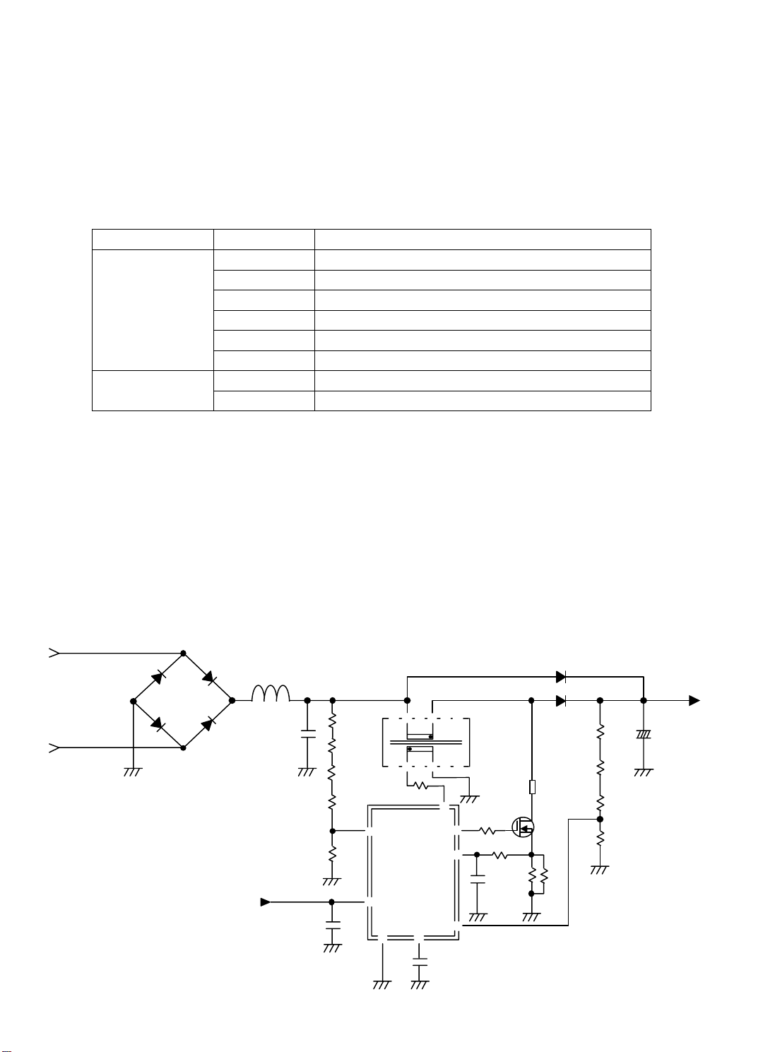
1.1.2 Rectifying circuit and higher harmonics suppression (active filter) circuit
The AC input voltage is rectified in the full wave mode with the diode bridge in D901 and input to pin 5 of
L903. The voltage of both end of C911 is the DC voltage approx. 390VDC boosted with the booster
circuit (active filter circuit) composed of IC901, Q901, L903 and D902. The active filter circuit compares
the voltage input to pin 1, pin 3 and pin 4 of IC901 and controls Q901 ON/OFF period so that the current
flows to L903 be sine-waved. The AC input current is sine-waved in the same phase with the input
voltage so as to improve the power factor, and the harmonic current is controlled consequently.
AC
D901
AC
From Sub power
Vcc
L902
C906
R908
C907
R904
R905
R906
R907
③
⑧
⑤
⑥
⑦ ⑧ ⑨ ⑩
R911
IC901
② ⑥
③ ④
②
⑪
⑤
C908
⑦
①
④
①
⑫
L903
R912
R909
R937
C910
D902
L905
Q901
R910
D933
R913
R914
R915
R917
To Main p o w e r
and sub power
+
C911
Fig. 1
Page 8
1.1.3 Sub power circuit
When the power switch is turned ON, the rectified and smoothed DC voltage (AC voltage x √2) is
supplied to pin 5 of IC903, and is charged to C930 through pin 1. When pin 1 reaches 5.7V, oscillation is
started in IC903, and the built-in output FET is put into operation to add the pulse voltage between pin 5
and pin 3 on the primary side of T902. The flyback voltage in proportion to the voltage on the primary
side is generated on the secondary side, then the DC voltage is generated with the half-wave rectifier
circuit composed of D971 and C971. The DC voltage generated at the secondary side is monitored by
IC922 through R976, R977 and R978. This information detected at IC922 is fed back to pin 1 of IC903
via PC902, and the ON period of output FET internal IC903 is controlled to keep the DC voltage on the
secondary side constantly. The flyback voltage in proportion to the voltage on the primary side is also
generated at pin 2 of T902. The pulse voltage generated at pin 2 of T902 is converted to the DC voltage
at D932 and C931, and supplied to pin 8 of IC901 and pin 4 of IC902 via Q902.
1.1.4 Main power circuit
When the P-SUS signal from microcomputer is turned to HI, Q902 is turned to ON, and the voltage approx.
+18V is supplied to pin 4 (Vcc terminal) of IC902 from pin 2 of T902.
When the voltage of pin 4 of IC902 reaches approx. +16V, oscillation is started in the circuit, and the
built-in output FET is put into operation to add the pulse voltage between pin 5 and pin 2 on the primary
side of T901. The flyback voltage generated at the secondary side in proportion to the one in the primary
side is rectified at D961, D963, D964, D965 and D967 and smoothed at C961, C963, C964, C965 and
C969 to generate the DC voltage. The DC voltage generated at the secondary side is monitored by
IC921 through R960, R961, R962 and R985. The information detected at IC921 is fed back to pin 1 of
IC902 via PC901, and the ON period of output FET internal IC902 is controlled to keep the DC voltage on
the secondary side constantly.
1.1.5 Demagnetizing circuit
When the power is turned ON or the manual demagnetizing function on OSM menu is set to ON, pin 47 of
IC102 on the main board is turned to HI, and Q950 and RL901 are also turned ON.
When RL901 is turned ON, the current flows to the demagnetizing coil, however, the demagnetizing
current gradually converges with the fever of TH902.
1.1.6 Power management circuit
This monitor carries the power management function. This function is effective only when being
connected with the personal computer carrying the power management function.
Mode H-SYNC V-SYNC State Display
NORMAL ON ON Displaying a picture Displaying a picture
SUSPENSION
The power consumption and the indication of Power-On Indicator for each mode are as follows.
Mode Power consumption Power-On Indicator
NORMAL 135W Green
SUSPEND 3W or less Orange
The control signal executes the power management function is output from microcomputer IC102. The
control signal is composed of two signals, SUSPEND and P-OFF. The operating state of each signal is
as follows.
Control signal name Pin of IC102 Normal Suspension
SUSPEND Pin 5 H L
P-OFF Pin 42 H L
OFF
ON
OFF
ON
OFF
OFF
No picture
CRT heater is
decreased voltage
mode (approx. 1.5V)
No raster
Page 9

1.2 Deflection processor block
1.2.1 Deflection processor (IC601)
Deflection processor IC601 horizontally compensates wise, position and distortion, and vertically controls
heights, position and linearity.
IC601 automatically tracks the frequency to output the appropriate horizontal/vertical drive pulse.
IC601 also outputs the horizontal parabola waveform for focus and the waveform for convergence
compensation.
1.2.2 Pressure-reduction type horizontal deflection power circuit (IC5C0)
IC5C0 compares the parabola waveform output from pin 64 of IC601 (this waveform controls the
horizontal width and distortion) with the sawtooth waveform (this waveform is synchronized with the
horizontal frequency) in order to output the +B drive pulse. The +B drive pulse output from pin 9 of IC5C0
will accumulate the 215V energy in T550 during Q5F1 ON period. During Q5F1 OFF period, the
accumulated energy will be released, and integrated by T550 and the S-shaped compensation capacitor.
The duty of this drive pulse depends on the DC level of the parabola waveform that is output from IC601.
1.2.3 Horizontal width control circuit
Q550 is controlled by the horizontal drive pulse that is output from IC601. When Q550 is ON, the energy
will be accumulated in the horizontal deflection yoke. When Q550 is OFF, the energy will flow into C550.
While repeating this operation, horizontal deflection will be carried out.
The collector pulse of Q550 will be subject to voltage division by C590 and C591, and the voltage-divided
pulse will be used for switching synchronization of the high-voltage control IC701 and also used as the
AFC pulse.
The duty of the +B drive pulse output from pin 9 of IC5C0 will be subject to change in order to control the
horizontal width. The parabola waveform output from IC601 is compared with the feedback waveform
output from T5C0 to obtain the comparison waveform, and this comparison waveform threshes the
sawtooth waveform inside IC5C0 in order to control the duty. If the duty is changed, the rectified voltage of
the S-shaped compensation capacitor will be changed, and the horizontal width will be also changed. The
vertical parabola waveform is generated inside IC601, and then mixed with the DC level for horizontal
width control. After that, the mixed parabola waveform will be output from 64 pin of IC601, and added to
IC5C0. This parabola output will be used for compensation of pin-cushion distortion, barrel distortion,
trapezoidal distortion, and upper/lower distortion.
1.2.4 Vertical deflection circuit
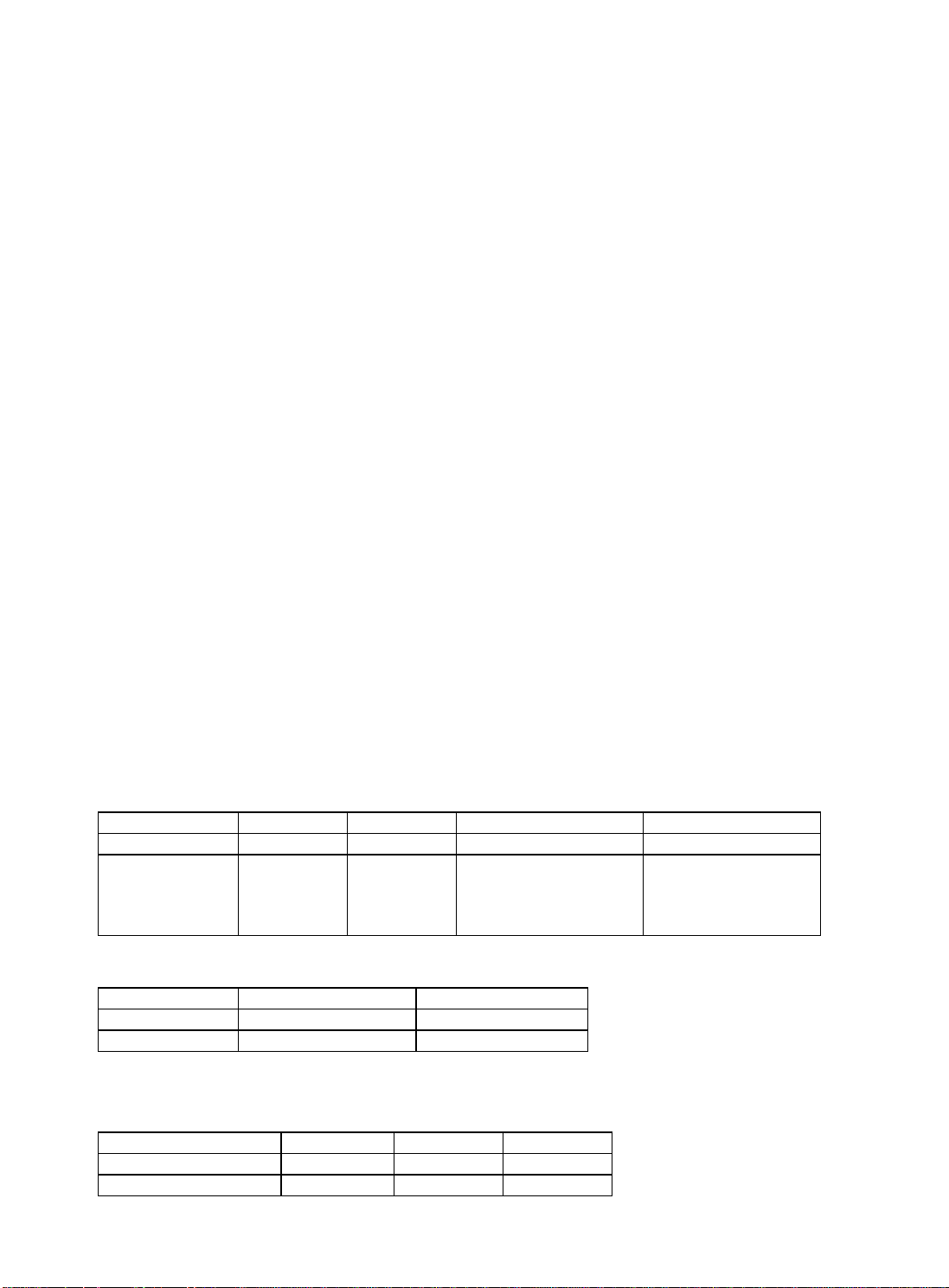
1.2.4.1 Sawtooth waveform generation, vertical size/position control, and linearity control circuit
If the vertical synchronization signal is input to 42 pin of IC601, the bipolar sawtooth waveform having the
same frequency as the input will be output from pins 1 and 11 of IC601. IC601 receives compensation
data from the MPU (IC102) to compensate the vertical size, vertical position, vertical raster position,
vertical linearity, and vertical linearity balance, and then outputs the compensated sawtooth waveforms
from pins 1 and 11. Pin 2 outputs the voltage to show the vertical deflection intermediate point.
The OP amplifier at the next stage outputs a signal to show the difference of the bipolar sawtooth
waveform. For this output, the RC low pass filter is adopted to eliminate the digital gradation of the output
waveform. In addition, pins 62 and 63 of IC601 will be turned ON during retracing operation in order to
prevent deterioration of the linearity and dispersion of scanning lines. Moreover, Q603 and Q604 are
switched depending on the vertical frequency in order to improve the linearity.
Page 10
IC601
VSAW-P
VSAW-N
IMID
11
63
62
1
2
R652
R650
R651
R637
R658
2
3
IC603
1
R645+R646
R642
R648+R649
R647
C628
IC603
5
6
Q604
Q603
7
SW-VLIN1
SW-VLIN2
Fig. 2 Vertical sawtooth waveform output circuit
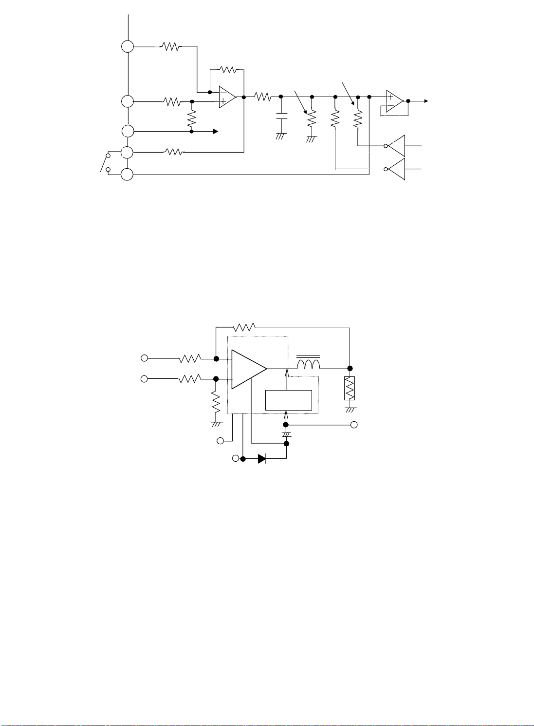
1.2.4.2 Vertical output amplification circuit
A current proportional to the waveform of the voltage input to IC401 will flow to the vertical deflection coil
(V-DY). R410 reads out the voltage waveform of the vertical deflection current, and then feeds back it to
IC401.
R419+R409
IMID
V SAW Input
R411
R405
R406+R418
-15.0V
5
4
+15.0V
-
+
1 6 3
IC451
D401
V-DY
2
Pump Up
7
C404
R410
VFLY
Fig. 3 Vertical output amplifier circuit
1.2.5 High voltage block
The high voltage block applies PWM control system that controls ON/OFF time of the high voltage
generation FET.
IC701 is the control IC that executes PWM control. The pulse voltage generated at Q701 is boosted at
T701 (FBT) to generate 27kV. To keep the high voltage stably, the feedback voltage from pin 10 of T701
is adopted, the control voltage from pin 56 of microcomputer IC102 is returned to pin 5 of IC701 and the
pulse wise of PWM output is controlled. PWM synchronizes with the horizontal frequency. Trigger pulse
for synchronizing is output from the divided collector pulse of the horizontal deflection output TR Q550,
and is input to pin 8 of IC701.
For adjustment of high voltage value, the voltage of pin 56 of IC102 is adjusted with the adjustment item
HV-ADJ-CAUTION on the OSM menu.
Page 11

1.2.6 DBF (Dynamic Beam Focus) circuit
The horizontal/vertical DBF voltage is respectively generated and amplified, then synthesized at T7A1.
As for the horizontal DBF voltage waveform, the parabola waveform voltage (approx. 0.5Vp-p) is output
with IC601, and amplified about 10 times with OP-AMP IC6A2. After that, it is amplified to 50-60Vp-p
with Q7B5 (the amplification factor is about 10 times), then it is amplified about 10 times with T7A1.
On the other hand, as for the vertical DBF voltage waveform, the parabola waveform voltage (approx.
1.0Vp-p) is output from IC601. It is amplified about 40 times at Q7A1, and the vertical parabola wave is
superposed to the horizontal parabola wave on the secondary side of T7A1, then consequently
synthesized. The collector pulse voltage of the high voltage output TR (Q701) rectified at D7A1 and
C7A1 is used for the power source of Q7A1. The synthesized DBF waveform is input to pin 12 of T701.
Page 12
1.3 Video block
1.3.1 Video signal amplifier circuit
D-SUB
CN216
B
2
1
G
2
4
R
3
6
D-SUB
CN215
B
1
10
G
2
12
R
3
14
1.3.1.1 Video clamp
SEL
13
IC 216
Anal og-sw
31
28
25
23
B
G
R
2
MPU
IC102
35 43 44
16 17 13
Retrace
BLK in
15
6
1
3
DAC
S/G SEL
18
SCL SDA
DAC
R-Bias
CLP-IN
IC 211
Pre - Amp
DAC
DAC
G-Bias
B-Bias
21 19 20
BIAS circuit
Fig. 4 Video signal amplifier circuit
10
14
IC 215
8
13
G
29
R
27
B
25
B OSD
11
G OSD
9
R OSD
10
OSD BLK
DET
40
11
8
9
17
19
18
IC 601
IC 210
MAIN
Amp
IC212
OSD
16
11
G
5
R
3
B
1
The clamp signal (positive polarity, 3.3 Vo-p) output from pin 35 of the MPU (IC102) is input to pin 13 of
IC211. The clamp signal is normally set to the back of the video signal (clamp position of OSM menu:
BACK). To correspond to the Sync on Green signal, the clamp signal can be set to the front of the video
signal (clamp position of OSM menu: FRONT). If the signal is a separate signal, changing the clamp
position of the OSM menu to FRONT or BACK will not change anything.
1.3.1.2 Video blanking
The horizontal/vertical retrace line (blanking) signal (positive polarity, 3.3 Vo-p) output from pin 40 of IC601
is input to pin 13 of IC215. IC215 reverses the polarity and amplifies the waveform (positive polarity,
3.3Vo-p -> negative polarity, 5.0Vo-p), and then reverses the polarity again (negative polarity, 5.0Vo-p ->
positive polarity, 5.0Vo-p) to output the blanking signal. This blanking signal is input to pin 14 of IC211 to
perform blanking operation during horizontal/vertical retracing operation.
To perform image blanking at switching the signal mode or at turning ON or OFF the power, the contrast
and the brightness will be set to MINIMUM.
1.3.1.3 Video mixing/amplifying
IC211 mixes the video signal with the OSM signal (G, R, and B signals of pins 9, 10, and 11) and with the
video blanking signal described in Sec. 1.3.1.2. I2C bus (pins 16 and 17 of SCL and SDA) fixes the black
level of the mixed video signal to 1.8V, and amplifies the mixed video signal (0.7Vp-p -> approx. 2.6Vp-p).
After that, the B, R, and G signals are output from pins 25, 27, and 29, respectively. The video signal
output from IC211 is input to IC210, where the signal is amplified (approx. 2.6Vp-p -> approx. 36Vp-p),
and the black level is fixed to 67V. After that, the B, R, and G signals are respectively output from pins 1, 3,
and 5.
1.3.1.4 Control of contrast and white balance
The MPU (IC102) sends the 8-bit contrast/white balance control data to IC211 with I2C bus (SCL, SDA
line). The contrast data simultaneously control 3 channels to simultaneously control the gains of the R, G,
and B, and the white balance data respectively controls the gains of the R, G, and B.
Page 13
1.3.2 Cut-off control circuit
p
G
5 GK
B
1
R
3
R250G R250R R250B
D250G D250B
R251R
D251G
C250G
Q251R
R253B
R252R
Q250R
C250B
R253R
D250R
D251R D251B
C250R
BK
RK
215V LINE
CRT
Pre-Am
R.BIAS
IC211
21 19 20
G.BIAS
B.BIAS
12V LINE
G
29
25 11
27
D264
R261
R260
B
R
Q250G
8
9
R251G
Q251G
R252G
IC210
MAIN-Amp
R251B
Q251B
R253G
R252B
Q250B
R255G
R256G
R255B
R254G
R256B
R254B
BRIGHT
R255R
R254R
R256R
IC213
IC102
1
3
55
MPU
2
Fig. 5 Cut-off control circuit
The cut-off control circuit consists of Q250R, Q250G, Q250B, Q251R, Q251G, and Q251B, and
simultaneously adjusts 3 colors (brightness), or individually adjusts 3 colors (biases of R, G, and B). The
microcomputer controls both types of adjustment.
1.3.2.1 Control of brightness
To simultaneously adjust 3 colors (brightness), the DAC voltage (0 to 5V, variable) line of microcomputer
pin 55 is connected to the emitters of Q250R, Q250G, and Q250B via IC213. This connection enables
simultaneous control of three TR collector currents and adjustment of the brightness.
1.3.2.2 Control of BIAS
To individually adjust 3 colors (biases of R, G, and B), the DAC output (1.5 to 5.5V, variable) lines (pins 19,
20, and 21 of IC211) are respectively connected to the emitters of Q250R, Q250G, and Q250B via I2C
bus of the microcomputer. This connection enables respective control of three TR collector currents and
adjustment of biases of the R, G, and B.
1.3.3 OSM (On Screen Manager)
IC212 is the OSM (On-Screen Manager), and displays the screens for screen adjustment, etc. The data to
be displayed on the OSM screens is sent to the MPU (IC102) via I2C bus.
Page 14
1.3.4 2 Input change circuit
The analog switch IC216 carries out the signal selection at the time of SIGNAL-A and B simultaneous
input. The signal selection is carried out by the SELECT signal of pin 3 of microcomputer IC102. By the
SELECT signal of pin 3, the input signal of SIGNAL-A is selected when pin 13 (SELECT SW) of the
analog switch IC206 is HIGH, and SIGNAL-B is selected when pin 13 (SELECT SW) of the analog switch
IC206 is LOW.
1.3.5 Sync on Green circuit
The Sync on Green signal input needs to make an image signal and a composite sync signal separate.
The separation method of the image signal and the composite sync signal is as follows. If a
microcomputer IC102 detects a Sync on Green signal, pin 18 S/G-SEL signals of IC211 will be set to
HIGH (5V), a transistor Q280 turns off, and the Sync on Green signal is output from pin 23 of IC216. The
Sync on Green signal output from pin 23 is input to pin 22 of IC216, it is divided to the image signal and
the composite sync signal at the inside of IC216, and only composite sync signal is output from pin 21.
1.3.6 Asset circuit
If the monitor power is turned OFF, 5V power will be supplied to pin 14 of EEPROM (IC217) from the PC
via pin 9 of CN216, and the data stored in the EEPROM (IC217) can be read out from I2C bus.
1.3.7 AUTO-SIZE function
The AUTO-SIZE function detects the phase data of RGB OR signal (output to pin 11 of OSM (IC212) from
pin 15 of AMP (IC211) from H-OSM and V-S signals input to pins 5 and 16 of IC212 in order to
automatically adjust the screen to the optimum width and position.
Using the OSM, select AUTO SIZE ADJUST, and then press (+) button to perform automatic size
adjustment.
1.3.8 SB MODE (Super Bright Mode) function
1.3.8.1 Adjustment item/operating function in selecting SB Mode
(*4): See (*4) mentioned in item 1.3.8.3.
→SUPER BRIGHT MODE OFF (in factory adjustment state)
↓
SUPER BRIGHT MODE-1 ON (PICTURE)
↓
SUPER BRIGHT MODE-2 ON (MOVIE)
↓
User adjustment items related to luminance/color coordination
Adjustment of
SUPER BRIGHT MODE
OFF
SUPER BRIGHT MODE-1
ON
SUPER BRIGHT MODE-2
ON
(*1): Brightness and contrast are common among three display mode.
(*2): For color temperature, the adjustment value is memorized in every display mode.
brightness
Adjustable (*1) Adjustable (*1) Selectable Selectable (*2) Adjustable (*4)
Adjustable (*1) Adjustable (*1) Not-selectable Selectable (*2) Not-adjustable
Adjustable (*1) Adjustable (*1) Not-selectable Selectable (*2) Not-adjustable
Adjustment of
contrast
Color mode
selection
Color
temperature
selection
Individual GAIN
adjustment
Page 15
SUPER BRIGHT MODE
OFF
SUPER BRIGHT MODE-1
ON
Back raster luminance GAIN UP
Normal Normal --- ---
Normal UP Presence ---
SUPER BRIGHT MODE-2
ON
UP UP Presence Presence
compensation
γ
1.3.8.2 Circuit (cathode) operation in selecting SB Mode [Window pattern]
SUPER BRIGHT MODE
SUPER BRIGHT MODE-1
ccordance
Amplitude: Approx. 36V
Amplitude: Approx. 44V
Same amplitude
GND
Sharpness
SUPER BRIGHT MODE-2
Amplitude: Approx. 44V
1.3.8.3 SB Mode setting data and control method
(OSM FACT3) Data name Data (hex)
Setting of back raster
luminance
Setting of GAIN UP
SBBR1 0 BRT UP value in SUPER BRIGHT MODE-1 ON "0"=No UP
SBBR2 32 BRT UP value in SUPER BRIGHT MODE-2 ON
SBCN1 3C
SBCN2 3C
Amplified value in SUPER BRIGHT MODE-1 ON
(see the following formula)
Amplified value in SUPER BRIGHT MODE-2 ON
(see the following formula)
GAIN UP formula = GAIN adjustment value (hex)(*3) x {1+ (Data (hex) of SBCN1 or SBCN2)/FF (hex) }
(*3): GAIN adjustment value is the following data (in OSM FACT3).
9300K R-GN1 G-GN1 B-GN1
6500K R-GN2 G-GN2 B-GN2
5000K R-GN3 G-GN3 B-GN3
(*4): When the SUPER BRIGHT MODE-1 or MODE-2 is ON, the GAIN cannot be adjusted as shown in the
table in Sec. 1.3.6.1 "Adjustment item/operating function in selecting SB Mode". However, when the
SUPER BRIGHT MODE is OFF, the MAX GAIN value calculated with the following formula will be written in
the following EEP address so that the GAIN value cannot be increased above that of the SUPER BRIGHT
MODE-1 and MODE-2 ON status.
MAX GAIN = Maximum value (hex) for R/G/B GAIN adjustment (*5) x {1 + (SBCN1 or SBCN2 data
(hex))/FF (hex)}
Page 16

(*5): R/G/B GAIN MAX value is the maximum one among GAIN adjustment value mentioned (*3) above.
EEP address (hex)
R G B
MAX GAIN 89 8a 8b
* Every R/G/B MAX GAIN data applied to the address listed above table are totally same.
In case of repair, after CRT, Pre-AMP (IC211), MAIN-AMP (IC210), etc. are replaced and the
luminance/color coordination is adjusted, the MAX GAIN value mentioned above should be rewritten.
1.3.9 CONSTANT BRIGHTNESS function
The brightness and color coordination of the screen will be deteriorated due to secular deterioration of the
CRT. The CONSTANT BRIGHTNESS function, however, will recover the deteriorated brightness close to
the initial level (level ensured at outgoing the factory).
If the CONSTANT BRIGHTNESS function is activated, operation will be performed at 106kHz horizontally
and at 85Hz vertically while ignoring the input signal, and the OSM-IC (IC212) will output the reference
image signal. In this condition, R744 detects the beam current flowing to pin 9 of the flyback transformer
T701. This beam current is inverted and amplified by IC703, and then converted into a voltage value by
the current/voltage conversion circuit. After that, the converted voltage value will be input to the A/D
converter (pin 27 of IC102 (microcomputer)). To individually detect the beam current values of 3 colors (R,
G, and B), the desired color only will be brightened by increasing the cut-off voltages of the other 2 colors.
After obtaining the beam current values of 3 colors in this way, the obtained beam current values will be
compared with the beam current values used for factory adjustment (beam current values stored in the
EEPROM). After that, the cut-off voltage values of 3 colors (R, G, and B) will be adjusted so that the beam
current values close to the factory adjustment values can be obtained. In this way, the cut-off conditions of
the CRT will be recovered close to the factory adjustment level.
In addition, if the CONSTANT BRIGHTNESS function is activated, the C_TIME_SEL signal input to the
base of Q704 will be set to the low level, Q704 is turned OFF, and the bias voltage will be applied to pin 5
of IC703. As a result, voltage proportional to the beam current value will be output from pin 7 of IC703. By
the way, difference in the flyback transformer or the CRT may cause difference in the beam current. To
eliminate such difference in the beam current, the DAC voltage (commonly used for the 6H-DC signal) can
adjust the bias voltage input to pin 5 of IC703 described above. During normal operation, the
C_TIME_SEL signal is set to the high level, Q704 is turned ON, and pin 5 of IC703 is grounded via the
GND line so that the output of IC703 pin 7 can be kept at the low level. The signal output from pin 7 of
IC703 is added to ABL signal with MD717 (Diode). When the CONSTANT BRIGHTNESS function is
activated, the ABL signal is input to pin 27 of IC102 as the beam current signal.
1.4 CRT compensation block
1.4.1 Earth magnetism cancel circuit
This model carries IC2S0 (geomagnetism sensor unit) that carries out the voltage conversion of the
magnetic field intensity of a north-south magnetic field and an east-west magnetic field. IC2S0 detects
the detected voltage and controls the various canceling functions described below automatically.
•South-north horizontal magnetic field rotation canceling function
•East-west horizontal magnetic field raster vertical position canceling function
•South-north horizontal magnetic field landing canceling function
•East-west horizontal magnetic field landing canceling function
•South-north horizontal magnetic field convergence canceling function
•East-west horizontal magnetic field convergence canceling function
Here, the output voltage of IC2S0 (earth magnetism sensor unit) operates as follows.
•South-north horizontal magnetic field (IC2S0 pin 5): 1.0V (-0.04mT) to 2.5V (+/-0.00mT) to
•Vertical magnetic field (IC2S0 pin 4): 4.0V (-0.04mT) to 2.5V (+/-0.00mT) to 1.0V (+0.04mT).
<Vertical magnetic field canceling function>
(a) Landing compensation
V-6H (Schematic Diagram) and PWB-V-6H (PWB) are added so that the CRT specified for Northern
Hemisphere ITC can be adjusted to the spec for Southern Hemisphere ITC.
4.0V(+0.04mT).
Page 17

Some circuits are also added to DEFL-SUB (Schematic Diagram) and PWB-DEFLSUB (PWB).
In PWB-V-6H a vertical sync. parabola waveform output from pin 59 of IC601 (1 bit DAC) is supplied
from pin 1 of CN804 and 300mAp-p parabola waveform (vertical sync.) current flows to the speed
modulating coil from pin 1 of CN8P2 via Q8P0 and Q8P1.
In PWB-DEFLSUB a vertical sync. parabola waveform output from pin 59 of IC601 (1 bit DAC) is
reversed and amplified via Q600 and it is associated to the horizontal phase deflection compensation
waveform output from pin 57 of IC601 to compensate side pin balance.
(b) Vertical magnetic filed landing cancel
The vertical magnetic field landing cancel circuit is the one to compensate the color shade and
deviation that reaches its maximum at the center in the horizontal axis direction and its minimum at
the upper and lower ends on the monitor surface.
The automatic adjustment is done by controlling DC level of the above 300mAp-p parabola waveform
flowing to the speed modulating coil installed in the neck part of CRT.
It is controlled by pin 46 of IC 102 (DAC "V CANCEL"), and controls the speed modulating coil with
DC level of +/-50mA by Q8P0 and Q8P1.
(c) Vertical magnetic field convergence cancel
The vertical magnetic field convergence cancel circuit is the circuit to compensate for the
misconvergence that results after the vertical convergence of RED and BLUE reversed at the upper
and lower ends on the whole display area of the monitor deteriorates, and it is automatically adjusted
by the saw-toothed waveform (vertical-frequency) current flowing to the 4V convergence
compensation coil mounted on DY. It is controlled with the AC component (YVJT & YVJB, vertical
frequency saw-toothed waveform) by pin 60 of IC601 (4V_SC), and saw-toothed waveform (vertical
frequency) current of +/-45mA (peak) is made to flow to the 4V convergence compensation coil by pin
6 of IC8A1 (PowerOpamp).
1.4.2 Rotation circuit
The rotation circuit is a circuit to compensate the picture inclination caused by the earth magnetism by
letting DC current flow to the rotation coil wound on the front side of DY for adjustment. It is controlled to
0 to 5V with the reference of 2.5V by IC102 pin 45 (PWM_DAC), and DC current of +/-100mA (max) is
made to flow to the rotation coil by IC804 pin 2.
This compensation circuit has two functions; (1) User adjustment (OSM display) and (2)
Southern/Northern horizontal magnetic field rotation cancellation.
1.4.3 East-west horizontal magnetic field vertical position canceling function
It is the function that detects the detection voltage change from IC2S0 (geomagnetism sensor unit) by
east-west horizontal magnetic field change, and cancels a changed part of a raster vertical position
automatically.
1.4.4 Corner purity circuit
The corner purity circuit is a circuit to compensate for the color shade and color deviation of the picture
corner. On the rear side of CRT, it is adjusted by DC current flowing to the corner purity coils installed in
the four corners on the display surface.
The compensation circuit is composed of the following five functions of (1) User adjustment (OSM display),
(2) Aging variation compensation, (3) High/low temperature drift compensation, (4) South-north horizontal
magnetic field landing cancel and (5) East-west horizontal magnetic field landing cancel.
(1) User adjustment (OSM display)
The user causes DC current of +/-60mA (max) to flow to the purity coil of each corner according to the
value displayed on OSM.
(2) Aging variation compensation
As the electronic beam collides with the aperture grille, it is thermally expanded and contracted. The
thermal expansion/contraction is varied according to the elapse of the power ON/OFF time of the
monitor. The color shade and deviation of the picture corner thus generated are automatically
adjusted.
The voltage of the beam current supply pin (T701 pin 9) is detected with R723/R724, and the voltage
that detects the time elapse of the power ON/OFF of the monitor is read from the CR charge
(integration) circuit composed of C723 and R738, and CR discharge (integration) circuit composed of
C723 and R737 through IC702 (buffer amplifier) by IC102 pin 26 (CPU_ADC), then, the DC current of
+/-19mA (max) flows to the purity coil on each corner according to the specified control program.
Page 18

(3) High/low temperature drift compensation
The front panel (glass) is thermally expanded and contracted as the temperature varies in the
installation environments of the monitor. The color shade and deviation of the picture corner are
automatically adjusted. The voltage that detects the temperature variation of the installation
environments of the monitor is read from the environment temperature detection circuit composed of
TH100 (thermistor) arranged near the front panel (glass) by IC102 pin 25 (CPU_ADC), and DC current
of +/-13mA (max) is made to flow to the purity coil on each corner according to the specified control
program.
(4) South-north horizontal magnetic field landing canceling function
North-south magnetic field landing canceling adjusts automatically the color irregularity and color
shading/impurity which are generated horizontal direction served as an opposite direction at the upper
end and lower end of a monitor display side. Detection voltage and a direction of the north-south
magnetic field (IC2S0 pin 5) are detected by IC2S0 (geomagnetism sensor unit) and pin 29
(CPU_ADC) of IC102 reads the detection voltage, and DC current of ±21mA (Max) is passed in each
corner purity coil according to the predetermined control program.
(5) East-west horizontal magnetic field landing canceling function
East-west horizontal magnetic field landing canceling adjusts automatically the color irregularity and
color shading/impurity which are generated horizontal direction served as an opposite direction at the
upper end and lower end of a monitor display side. Detection voltage and a direction of the
north-south magnetic field (IC2S0 pin 4) are detected by IC2S0 (geomagnetism sensor unit) and pin
28 (CPU_ADC) of IC102 reads the detection voltage, and DC current of ±21mA (Max) is passed in
each corner purity coil according to the predetermined control program.
1.4.4.1 Corner purity circuit operation
<TL: Upper left corner>
Pin 50 (PWM_DAC) of IC102 controls the TL in the range of 0 to 5V while regarding 2.5V as the reference
voltage, and the DC current of the above value will flow from pin 2 of IC803 to the upper left corner purity
coil.
<TR: Upper right corner>
Pin 49 (PWM_DAC) of IC102 controls the TR in the range of 0 to 5V while regarding 2.5V as the reference
voltage, and the DC current of the above value will flow from pin 8 of IC803 to the upper right corner purity
coil.
<BL: Lower left corner>
Pin 52 (PWM_DAC) of IC102 controls the BL in the range of 0 to 5V while regarding 2.5V as the reference
voltage, and the DC current of the above value will flow from pin 2 of IC801 to the lower left corner purity
coil.
<BR: Lower right corner>
Pin 51 (PWM_DAC) of IC102 controls the BR in the range of 0 to 5V while regarding 2.5V as the
reference voltage, and the DC current of the above value will flow from pin 8 of IC801 to the lower right
corner purity coil.
1.4.5
The vertical magnetic field landing cancel circuit is the circuit to compensate for the color shade and
deviation that reaches its maximum at the center in the horizontal axis direction and its minimum at the
upper and lower ends on the monitor surface, and the adjustment is done by DC current according to the
value displayed on OSM flowing to the speed modulating coil installed in the neck part of CRT.
It is controlled with 0 to 5V of 2.5V reference by IC102 pin 46 (PWM-DAC), and DC current of +/-150mA
(max) is made to flow to the speed modulating coil by IC804 pin 8.
1.4.6 Digital dynamic convergence clear (DDCC) circuit
In the digital dynamic convergence clear (hereafter called DDCC) circuit, the convergence compensating
current waveform is produced and amplified, and the convergence is compensated by the compensation
current flowing to the sub yoke that is installed as the rear unit of the deflection yoke.
Though the principle of the convergence compensation with the sub yoke is same as the CP ring, the CP
Vertical magnetic field landing cancel circuit
Page 19
ring is used for the static variation with the parallel movement in the whole picture in the uniform magnetic
field with the permanent magnet but the sub yoke is used for dynamic variation that compensates a
desired position on the picture by controlling the current waveform that flows to the coil of the electric
magnet. (See Fig. 7)
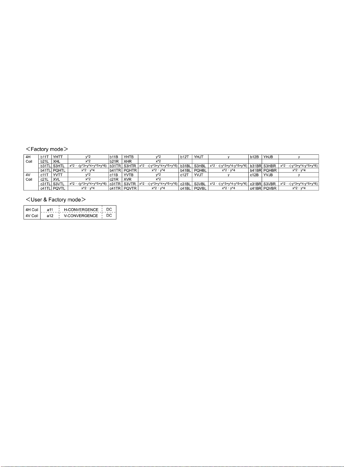
1.4.6.1 Production of compensation current waveform
There are 30 kinds of compensation elements, and they are programmed in IC601 one by one using the
function. Inputting the compensation coefficient into the function controls the amplitude of the current.
Examples of the functions and current waveform/compensation operation of YH (YHTT, THTB, YHJT,
YHJB) are shown as follows.
In the above formulas, b11T, b11B, b12T and b12B express the compensation coefficients, and y and y^2
express the primary and secondary functions of the vertical frequencies.
The other parts except the compensation coefficients are programmed, and desired amplitudes (=
compensation amount) are gained by varying the coefficients.
YHTT and YHTB compensate the upper and lower parts of the picture of the characteristic components of
their DYs to compensate the upper and lower parts of the picture of the axis deviation component. The
component gained by adding YHT and YHJ is multiplied by the offset compensation coefficient a11. The
resultant component is regarded as 4H_SC, and is output from IC601 pin 61.
1.4.6.2 Waveform, and operation on the picture
The case in which the currents flow through 4H coils of the sub yoke is explained. Regarding YHT
(secondary function in the vertical frequency), in case of Fig. 6 as an example, the current is large in the
same direction at the start (upper end of the picture) and the end (lower end of the picture) of the vertical
frequency, and is zeroed on the X axis of the picture. Therefore, the magnetic field that is proportional to
it is generated, and RED and BLUE vary in the same direction only at the upper and lower ends of the
picture. As aforementioned, YHT can be independently controlled at the upper part (b11t・y^2) and lower
part (b11B・y^2).
Moreover, regarding YHJ (primary function in the vertical frequency), if the flowing direction of the current
is opposite at the start (upper end of the picture) and the end (lower end of the picture) of the vertical
frequency as an example, RED and BLUE vary in the opposite direction only at the upper and lower ends
of the picture. Making the current flow to the 4V coil can do compensation in the vertical direction.
Fig. 8 (a) and (b) shows the image of each adjustment item of the DDCC adjustment.
Fig. 6 DDCC compensation image
Page 20
1.4.6.3 Adjustment method
Before the adjustment with the compensation circuit, it is necessary that they are properly adjusted at the
center (H-STATIC and V-STATIC), on the X axis (XH slider, B-Bow 4P, XV differential coil) and on the Y
axis (YH volume, YV volume).
Though DC current is superimposed on the sub yoke, H-STATIC and V-STATIC are pushed to the greatest
possible extent by the adjustment with CP ring in order to reduce the stress of the driver IC8A1
(STK391-110).
Moreover, although 6H coil is carried in the case of this chassis, in addition to 4H and 4V coils, since the
range which can be adjusted is a range used as fine adjustment, it is a premise that the convergence
between Red, Blue and Green (6H and 6V) is in a standard as a performance of ITC (CRT&DY) in the
state where 6H coil is not used.
As the adjustment procedure, the adjustment values of 30 elements are not respectively zeroed but they
are adjusted to nearest to zero with a total balance in good order.
In other words, the balance (compromise) adjustment with each adjustment item is applied.
The correspondence of the names of DDCC adjustment mode to the coefficients of all 30 elements is
shown below.
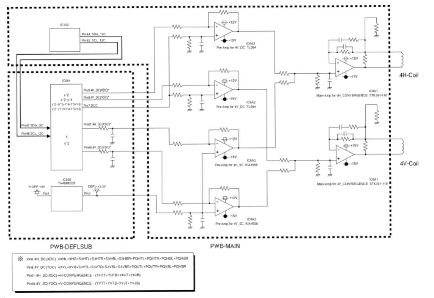
1.4.6.4 Block diagram
Fig. 9 shows the block diagram of the DDCC circuit.
The components 4H_DC (pin 6), 4H_SC (pin 61), 4V_DC (pin 8) and 4V_SC (pin 60) supplied from IC601
to 4H-Coil and 4V-Coil are output, the dynamic component (4H_DC, 4V_DC) is amplified with IC6A2, and
the static component (4H_SC, 4V_SC) is amplified with IC6A3.
DDC (pin 7) output from IC601 and DEFL_+3.3V (pin 3) output from IC602 are respectively the reference
voltage of Op-Amp (IC6A2) that amplifies the above dynamic component (4H_DC, 4V_DC) and the
reference voltage of Op-Amp (IC6A3) that amplifies the static component (4H_SC, 4V_SC).
On each of 4H and 4V, the waveform added with the dynamic component and static component is input to
IC8A1 pin 3 and pin 4, and it allows the specified current to flow to each convergence compensation coil.
Page 21
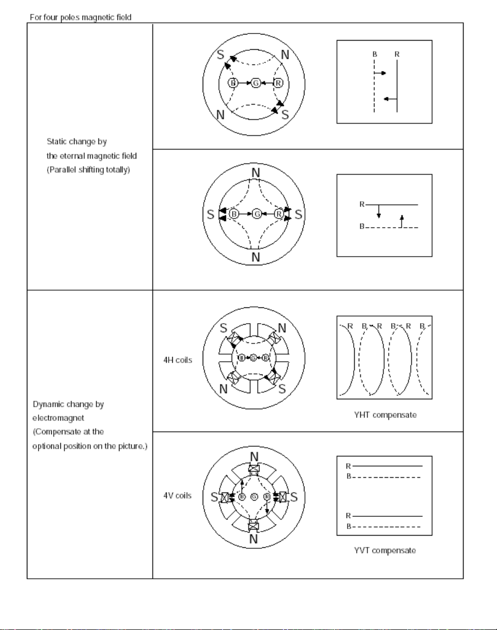
Fig. 7 The principle of DDCC compensation
Page 22
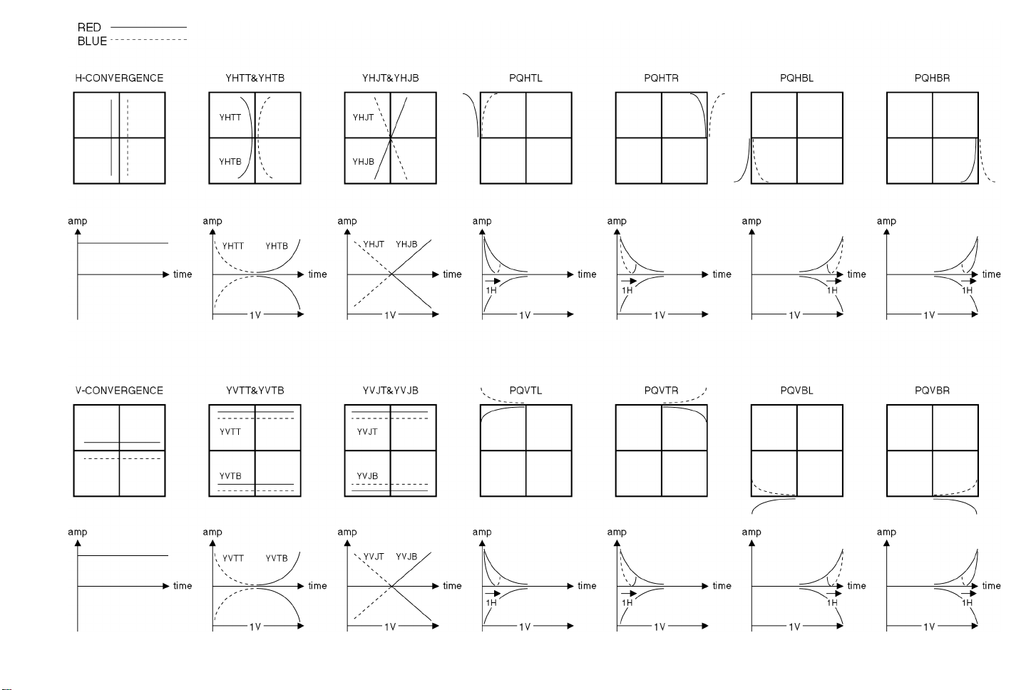
Fig. 8 (a) DDCC adjustment item
Page 23
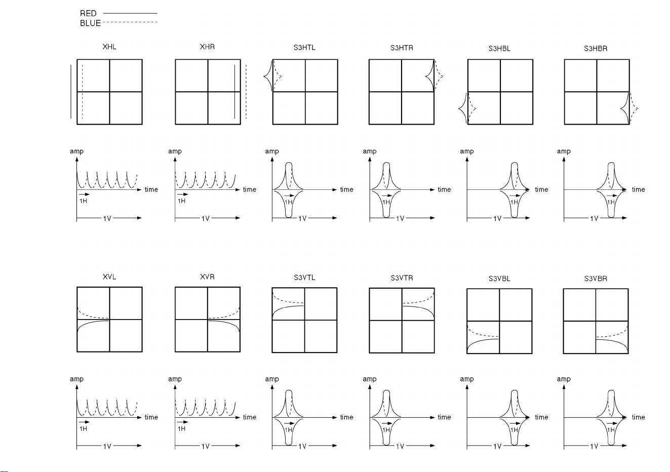
Fig. 8 (b) DDCC adjustment item
Page 24
Page 25
1.4.7 East-west horizontal convergence canceling function
It is the function which rectifies automatically change of YHJT, YHJB and XVL, and XVR (between Red
and Blue) by east-west magnetic field change, detects the detection voltage change from IC2S0
(geomagnetism sensor unit), and is carrying out automatic compensation.
1.5 USB circuit
1.5.1 Outline
This monitor loads the standard USB SELF POWERED HUB with 1 upstream and 4 downstreams.
(1) Serial data bus
Data bus is connected from upstream connector CN1A0 to upstream port of HUB controller IC1A0, and
downstream connectors CN1A1 to CN1A4 are connected from HUB controller.
HUB controller relays data communication between the upstream side (PC) and the downstream side
(device).
Downstream connection of HUB controller
Port on circuit diagram Connector Silk indication
Port 1 CN1A1 1
Port 2 CN1A2 4
Port 3 CN1A3 3
Port 4 CN1A4 2
(2) Power supply to downstream
USB HUB of this monitor is SELF POWERED HUB, and it can supply the power of +5V 500mA (max)
to each downstream from transformer T902 on PWB-MAIN. Further, HUB controller IC1A0 has the
function of detecting overcurrent, and stops supplying the power to each downstream port when
overcurrent (500mA or more) is detected at each port.
1.5.2 USB downstream power supply
(1) Supply of Vpp power
When HUB controller IC1A0 is recognized from the direction of upstream, the signal which functions
as a switch of power output for a downstream port is output (IC1A0 pins 2, 16, 17 and 32).
When IC1A0 pins 2, 16, 17 and 32 become LOW, FET gates are turned ON (LOW), and EFT
transistors Q1A1, Q1A2, Q1A3 and Q1A4 supply the power to the downstream ports (CN1A1 to
CN1A4) respectively.
(2) Detection of overcurrent
HUB controller IC1A0 has the function of detecting overcurrent. If the current output at each port
exceeds 550mA (min), gates of FET transistors Q1A1, Q1A2, Q1A3 and Q1A4 turn OFF (HIGH),
automatically output of current stops only to the port that overcurrent is detected.
In order to re-operate the port that overcurrent is detected, either of the followings should be carried
out:
1.OFF/ON of monitor power supply
2.Pulling-out and pulling-in of upstream cable
3.Restart of PC
1.5.3 HUB controller power output
HUB controller IC1A0 has a built-in 3.3V regulator, and outputs from IC1A0 pin 1.
1.5.4 USB power on reset
At the time of a power ON and spark detection circuit operation, the reset pulse to USB is output to pin 21
of IC1A0 from pin 2 of IC102. At pin 21 of IC1A0, it is reset by LOW and is reset release by HIGH.
Page 26

1.6 Control block
1.6.1 Function of control circuit
The control block is mainly on MAIN board and DEFL-SUB board, and the function is as follows.
(1) Auto-tracking
(2) Control of picture size, distortion and position
(3) Adjustment data memory
(4) Sync. signal detection
(5) OSM control
(6) Video pre-amp control and clamp pulse position control
(7) Power ON/OFF control
(8) Heater voltage control
(9) DDC 1 / 2B / 2Bi
(10) Operating time display
The control block is composed of the following four components.
(1) Microcomputer: IC102 (MAIN board)
(2) OSM IC: IC212 (VIDEO board)
(3) EEPROM: IC104 (MAIN board)
(4) Sync. signal input: IC215 (VIDEO board)
1.6.2 Auto-tracking process
The microcomputer (IC102) calculates the frequency of the sync. signal input and outputs the distortion
compensation data corresponding to the input signal timing to the deflection IC (IC600).
Control with IC600 is carried out via I2C bus.
1.6.3 EEPROM
The capacity of the EEPROM (IC104) is 32 kilobits (4 kilobytes). The factory adjustment data, user
adjustment data, and EDID data are stored in the EEPROM.
Up to 10 items can be stored as the factory preset data, and up to 16 items can be stored as the user
preset data. Regarding the factory preset timing, if the user reset the memory, the factory adjustment data
will be called up.
The EDID data is stored in the last 128-byte area.
1.6.4 On-Screen-Manager (OSM) controller
The On-Screen-Manager (OSM) controller IC IC212 displays the picture used for picture adjustment and
so on. OSM display data is sent from the microcomputer (IC102) via I2C bus.
1.6.5 Heater voltage control
In the normally ON status, the heater voltage is supplied from the +8V line of the main power circuit.
Heater resistor R203H connected in series adjusts this supplied voltage to +6.15V (typ) (rated voltage for
the CRT) before application. In the suspend mode, the sub-power circuit applies the voltage so that the
screen can be instantaneously recovered. (In the suspend mode, the heater voltage is low compared with
that of the normally ON status.)
1.6.6 Protection circuit operation
This monitor can detect the following problems, and can stop the monitor operation after detection of a
problem. If the protector function is activated, the Power-On Indicator (LED) will flicker so that you can
localize the activated protector.
1.6.6.1 X-ray protector
The CRT monitor radiates X-rays, and exposure to too much radiation is very dangerous. For this reason,
the CRT monitor incorporates an X-ray protector. If the high voltage value rises above the specified value,
the protector will automatically stop applying the high voltage. For this model, the X-ray protector
activation point is set to 31.0kV (entirely black screen).
To disable the X-ray protector for the reason of repair, etc., set the monitor in the factory mode.
Page 27
1.6.6.2 High voltage data error detection
Important safety data, such as the high voltage adjustment value and the X-ray protector activation
voltage, are stored in the EEPROM. For each safety data, there is backup data. If both data values differ
from each other, the monitor will enter the power saving mode (the high voltage will not be applied).
1.6.6.3 Beam current protector
If too much beam current flows (1.5mA or more), "H" will be input to the ABL terminal (pin 27 of the
microcomputer (IC102)). From this terminal, the microcomputer will detect overflow of the beam current,
and will set the monitor in the power saving mode.
1.6.6.4 Power-On Indicator (LED) flickering pattern in each protector operating
If a protector is activated, the Power-On Indicator (LED) will flicker as shown below to indicate the
activated protector (to show the cause of the problem).
Table 2 Power-On Indicator (LED) flickering pattern in each protector operating
Protector state
X-ray protector 1 1
High voltage circuit latch
detection
Data protector 3 1
Short (0.5s) lighting times Long (2s) lighting times
Power-On Indicator (LED) state
2 1
Beam protector 5 1
+B short-circuit 7 1
1.6.6.5 Operating time
If "DIAGNOSIS" is selected from the menu in the factory mode, the monitor operation time will appear. 0.5
hours will be added to this value every 30 minutes.
P: Indicates the power-on time (including the operation time in the power saving mode).
K: Indicates the heater power-on time.
1.6.6.6 The DDC communication
The microcomputer carries out the DDC communication. For this communication, the microcomputer
reads out the EDID data from the EEPROM, and stores the data in the RAM. When receiving a request
from the PC, the microcomputer will output the data from pins 8 and 11.
Page 28
1.6.6.7 Microcomputer pin assignment
#
1 H_LOCK
2
3 INPUT SEL
4 HSK
5 SUSPEND
6 C TIME SEL
7 OPTION
8 DDC_DATA
9 FLASH_TX
10 BEAM/SHORT RxD0/P50
11 DDC_SCL
12 RESET
13 NMI
14 (+) 5V
15 STBY
16 GND
17 X'TAL
18 X'TAL
19 MODE SW1
20 MODE SW2
21 GND
22 KEY1
23 KEY2
24 X RAY PRO
25 TEMP
26 BEAM TIME
27 ABL/C TIME
28 EW_SENSE
29 SN_SENSE
30 Vcc
31 LED
32 VSYNC OUT VSYNCO/P61 O V. sync. output
USB-SPARK
USB-RESET
PORT
ASSIGN I/O
IRQ2/P40
IRQ1/P41
IRQ0/P42
RD/P43
WR/P44
IOS/AS/P45
EXCL/o/P46
SDA0/WAIT
TxD0/P50
SCL0/SCK0
RES
MNI
Vcc
STBY
GND
XTAL
EXTAL
SW1
SW2
AVs s
AN0/P70
AN1/P71
AN2/P72
AN3/P73
AN4/P74
AN4/P75
AN6/P76
AN7/P77
AVc c
HFBACK/P60 O LED output
I H_UNLOCK detection
I/O For FLASH writ ing
O Power cut detection
O SOA output
O Suspend
O
I
I/O DDC data
O PZTAT
I Beam protector
I/O DDC clock
I Reset
I NMI
I
A/D Key input
A/D Key input
A/D X-ray protector
A/D Temp. detection
A/D Time detection
A/D Heater voltage detection 38 Hsync OUT
A/D
A/D
FUNCTION
(available as input port)
Mode setting
Mode setting
H. magnetic field detection
V. magnetic field detection
#
64 CS8
63 CS7
62 CS6
61 CS5
60 CS4
59 CS3
58 CS2
57 CS1
56 HVADJ
55 BRIGHTNESS P11/PWMX1 P Brightness
54 SW LIN2
53 SW LIN1
52 PURITY_BL
51 PURITY_BR
50 PURITY_TL
49 PURITY_TR
48 GND
47 DEGAUSS
46 V_CANCEL
45 ROTATION
44 IIC_SDA
43 IIC_SCL
42 P OFF
41 LIN PWM1
40 6H
39 Vcc
37 SOG IN
36 HSYNC IN
35 CLAMP OUT
34 HSYNC SEL
33 VSYNC IN
PORT
ASSIGN I/O
P37
P36
P35
P34
P33
P32
P31
P30
P10/PWMX0 P HVADJ
O CS switching 8
O CS switching 7
O CS switching 6
O CS switching 5
O CS switching 4
O CS switching 3
O CS switching 2
O CS switching 1
FUNCTION
P12/PW2
P13/PW3
P14/PW4
P15/PW5
P16/PW6
P17/PW7
Vss
P20/PW8
P21/PW9
P22/PW10
SDA1
SCL1
P25/PW13
P26/PW14
P27/PW15
Vcc
P67/HSYNCO O H. sync. output
P66/CSYNCI I SYNC ON G input
P65/HSYNCI I H. sync. input
P64/CLAMPO O CLAMP OUT
P63/VFBACKI O HSYNC SEL
V_SYNCI
O SW LIN2
O SW LIN1
P Corner purity BL
P Corner purity BR
P Corner purity TL
P Corner purity TR
O
P
P Rotation
I/O Internal IIC data
I/O Internal IIC clock
O POWER OFF
P H. linearity
P 6H
I V. sy nc . i np u t
DEGAUSS
V. m agnetic field cancel output
Page 29

1.7 X-ray protection circuit and safety protection circuit
1.7.1 X-ray protection circuit
This circuit prevents X-ray radiation from exceeding the dangerous level due to the abnormal rise of high
voltage.
Do not modify the high voltage circuit and the safety protection circuit.
The upper limit of the high voltage value and the beam current value are determined by the X-ray radiation
upper limit curve of CRT.
In the X-ray protection circuit, the X-ray protector activation voltage depends on the beam current. The
X-ray protector, however, is normally activated at approximately 30kV (when the beam current is
approximately 1mA). D709 and C704 rectify the increase in the pulse voltage output from pin 6 of T701.
Pin 24 of IC102 detects this rectified voltage. If the detected voltage exceeds the specified value, the
SUSPEND signal output from pin 5 of IC102 will be set to 'Low', and the P-OFF signal output from pin 42
will be also set to 'Low' (power-off mode). In addition, operation of IC701 will be stopped. This condition of
the protection circuit will be retained until the power switch is turned OFF.
1.7.2 Beam current protection circuit
When the current supplied to the high voltage generating winding of FBT exceeds approx. 1.5mA, the
protection circuit functions. The detection of the beam current is executed by the voltage fall of R722
connected between T901 pin 9 and the 12V.
Resistors R723 and R724 divide the potential of this voltage. The divided voltage is then input to pin 27 of
IC102 via IC703. If the input voltage exceeds the specified value, the SUSPEND signal output from pin 5
of IC102 will be set to 'Low', and the P-OFF signal output from pin 42 will be also set to 'Low' (power-off
mode). In addition, operation of IC701 will be stopped. This condition of the protection circuit will be
retained until the power switch is turned OFF.
1.7.3 IC701 overcurrent protection circuit
The peak value of the drain current of Q701 and the both-end voltages of source resistors R708 and R709
are detected by pin 2 of IC701. If the voltage of this pin exceeds 1.2V (typ), pin 9 of IC701 will stop
outputting the drive waveform. If the voltage of IC701 pin 2 drops below 1.2V (typ), pin 9 of IC701 will
output the drive waveform again.
1.7.4 IC701 overload protection circuit
If overload occurs consecutively and the overcurrent protection circuit is activated consecutively, this
overload protection circuit will enter the latch mode to stop operation. If the voltage of IC701 pin 2 exceeds
1.0V (typ), C709 will be charged. If the voltage of IC701 pin 13 exceeds 2.5V (typ), IC701 will enter the
latch mode to stop the control operation. This condition of the protection circuit will be retained until the
power switch is turned OFF.
1.7.5 IC902 overcurrent protection circuit
IC902 is equipped with an overcurrent protection circuit. R928 detects the drain current of the incorporated
FET. If the voltage of IC902 pin 1 exceeds approximately 0.7V, this overcurrent protection circuit will be
activated.
1.7.6 Short-circuit protection circuit on secondary power side
The output line of each secondary power (+215V, +80V, +15V, +8V, -15V) is equipped with a short-circuit
detection circuit. If a secondary line is overloaded and the output voltage drops by 30 to 40% of the normal
voltage, this short-circuit protection circuit will be activated.
1.7.7 Overvoltage protection circuit
The harmonic suppression circuit (active filter circuit) and the main power circuit are respectively equipped
with an overvoltage protection circuit. If the voltage between both ends of C911 rises by 10% of the normal
voltage, or if the voltage of the main power secondary output line rises by 30 to 40% of the normal voltage,
operations of IC901 and IC902 will be stopped.
Page 30
1.8 Adjustment
1.8.1 Adjustment mode
This monitor has the following adjustment modes.
(1) User mode (Normal mode)
(2) Factory mode (Factory adjustment mode)
1.8.2 User mode (Normal mode)
This is the mode user executing the adjustment and setting. When pressing button of EXIT, (<), (>), (-),
(+) and SELECT on the front panel, the following menu picture is displayed on the screen.
The adjusted data in the user mode is memorized to EEPROM automatically.
The adjustment group can be selected with (<), (>), (-) and (+) buttons.
(+) and (-) buttons have the functions of the variable of the adjustment value.
The items can be adjusted in the user mode are as following table.
Page 31

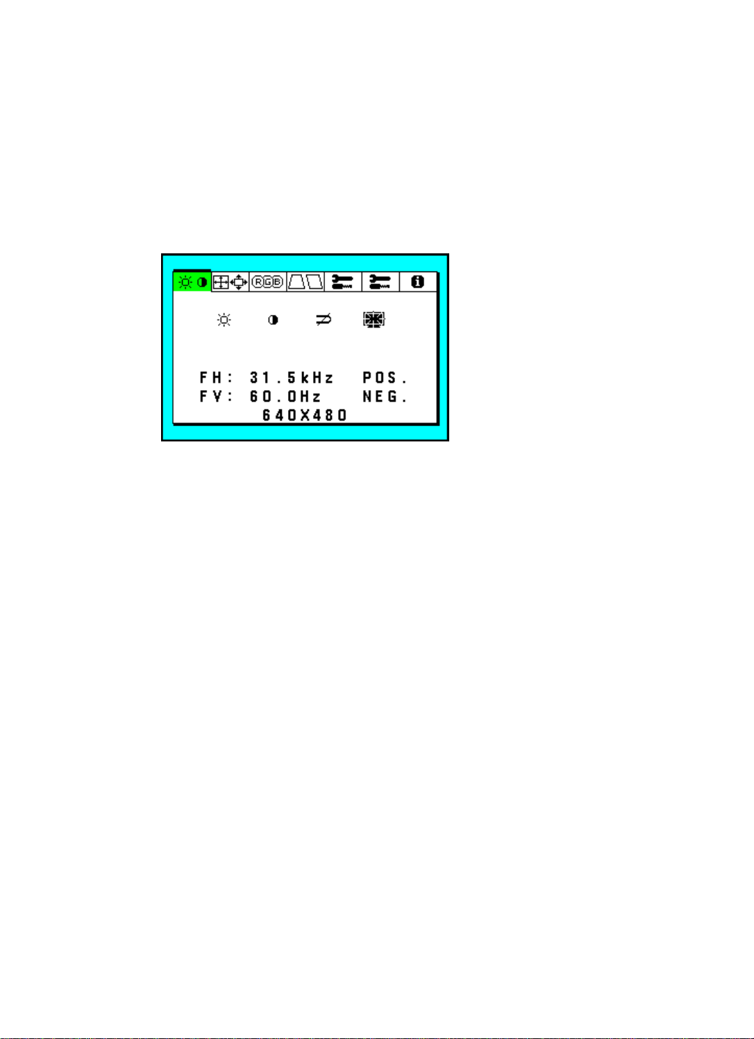
OSM menu (User mode)
Item
Group icon
icon
Group 1
RESET
Item
BRIGHTNESS
CONTRAST
DEGAUSS
CONSTANT BRIGHTNESS
AUTOADJUST
LEFT / RIGHT
Adjustment
− +
To decrease the
brightness.
To decrease the contrast.
N/A
N/A
Restore to factory preset level with RESET
button.
N/A
To move the image
to the left.
To increase the brightness.
To increase the contrast.
To eliminate possible
color shading or impurity.
Activates the constant
brightness function.
To adjust the screen
size automatically
based on input timing.
To move the image to
the right.
Group 2
Group 3
Group 4
DOWN / UP
NARROW / WIDE
SHORT / TALL
RESET
COLOR TEMPERATURE ADJUSTMENT
(9300K, 8200K, 7500K, SRGB, 5000K)
For each
color
temperature
RESET
IN / OUT (PIN CUSHION)
LEFT / RIGHT (PIN CUSHION
BALANCE)
TILT (PARALLELOGRAM)
ALIGN (TRAPEZOIDAL)
ROTATE (RASTER ROTATION)
TOP
TOP-BALANCE
BOTTOM
COLOR
TEMPERATURE
RED
GREEN
BLUE
To move the image
down.
To narrow the width of
the image on the screen.
To narrow the height of
the image on the screen.
Restore to factory preset level with RESET
button.
N/A
To decrease the
color temperature.
To decrease the red color.
To decrease the green
color.
To decrease the blue color.
Restore to factory preset level with RESET
button.
Forms a pin. Forms a barrel.
Distorts the screen
leftward.
Distorts the upper
section leftward.
Narrows the upper
section.
To rotate the image
counterclockwise.
The upper section
forms a pin.
Distorts the upper
section leftward.
The lower section
forms a pin.
To move the image
up.
To expand the width of
the image on the screen.
To expand the height of
the image on the screen.
N/A
To increase the color
temperature.
To increase the red color.
To increase the green color.
To increase the blue color.
Distorts the screen
rightward.
Distorts the upper
section rightward.
Narrows the lower
section.
To rotate the image
clockwise.
The upper section
forms a barrel.
Distorts the upper
section rightward.
Lowers the lower
section.
BOTTOM-BALANCE
RESET
Distorts the lower
section leftward.
Restore to factory preset level with RESET
button.
Distorts the lower
section rightward.
Page 32

Group icon
Group5
Item
icon
MOIRE CLEAR
CONVERGENCE (HOR.)
CONVERGENCE (VER.)
LINEARITY (VER.)
VERTICAL BALANCE
GLOVAL SYNC (TL)
GLOBAL SYNC (TR)
GLOBAL SYNC (BL)
GLOBAL SYNC (BR)
GLOBAL SYNC (L / R)
Item
RESET
LANGUAGE
Adjustment
−
Reduces the moire
value.
The red moves to
the left side of the
green.
The red moves
below the green.
Contracts the
center area.
Elongates the lower
section of the
screen.
The green screen
will be reddish.
The green screen
will be reddish.
The green screen
will be reddish.
The green screen
will be reddish.
The both side of the
screen will be
reddish.
Restore to factory preset level with RESET
button.
Selects the left
items.
Increases the moire
value.
The red moves to the
right side of the green.
The red moves above
the green.
Elongates the center
area.
Elongates the upper
section of the screen.
The green screen will
be bluish.
The green screen will
be bluish.
The green screen will
be bluish.
The green screen will
be bluish.
The both side of the
screen will be bluish.
Selects the right item.
+
Group 6
Group 7
OSM POSITION
OSM TURN OFF
OSM LOCK OUT
IPM OFF MODE
EDGE LOCK
HOT KEY
FACTORY PRESET
RESET
DISPLAY MODE
MONITOR INFO
REFRESH NOTIFIER
RESET
C→BR→BL→TR
TL
→
Reduces the time. Increases the time.
N/A
ON OFF
FRONT BACK
ON OFF
N/A
Restore to factory preset level with RESET
button.
N/A N/A
N/A N/A
ON OFF
Restore to factory preset level with RESET
button.
C→TL→TR→BL
BR
Turns ON (+: SELECT
key)
Restores all items to
the factory preset
level.
→
* Reset: Select an adjustment item and press the RESET key, then, it restores to factory preset level.
Page 33

1.8.3 Factory mode
This mod can adjust all of items, and also change the factory default adjustment data (reset data).
1.8.3.1 How to entering to Factory mode
The setting of the factory mode is executed by the following procedures.
(1) Power ON with EXIT button pressed, and confirm that the following OSM picture appears.
H2---- OW---- 01
FACT DATA
(3) Press (-) button once to set the data value to 255.
(4) Press (+) button to set the data value to 5.
(5) Press SELECT button to move to the factory mode.
(6) As shown below, the adjustment data (hexadecimal number) and the adjustment group of FAC1,
FAC2 and FAC3.
1.8.3.2 How to cancel Factory mode
Follow the procedure below to cancel the factory mode:
(1) Using the (>) button, select the FAC3 group, and then press the (>) button again. The following OSM
picture will appear.
H2---- OW---- 01
FACT DATA
(2) Press the (+) or (-) button to set the data value to '10'.
(3) Press the (SELECT) button. The factory mode will be canceled.
1.8.3.3 How to enter FACTORY-HV mode
Follow the procedure below to enter the FACTORY-HV mode:
(1) Using the (>) button, select the FAC3 group, and then press the (>) button again. The following OSM
picture will appear.
H2---- OW---- 01
FACT DATA
Page 34

(2) Press the (-) button to set the data value to '250'.
(3) Press the (SELECT) key to enter the FACTORY-HV mode.
(4) Press the (>) or (<) button. The FACTORY-HV mode will be canceled.
Page 35

2. Adjustment procedure
s
2.1 Measuring instruments
(1) Signal generator A: Astro Design VG-812 or equivalent
(2) Signal generator B: Astro Design VG-829 or equivalent
(3) DC voltmeter: 150V 0.5 Class or digital voltmeter
(4) High voltage meter: 0.5 Class that can measure 40KV
(5) Luminance meter: Minolta color analyzer CA-100 or equivalent
(6) AC voltmeter: 150V/300V 0.5 Class or equivalent
(7) Oscilloscope: Scope with band of 100MHz or more
(8) Landing measuring device: Felmo product
(9) Double scale: For width and distortion measurement
(10)Withstand voltage meter: Kikusui Model TOS8650 or equivalent
(11)Grounding conductivity measuring instrument: CLARE U.K. product
(12)Convergence meter: MINOLTA CC-100
2.2 Preparatory inspections
(1) There must be no cracks or remarkable contamination on the PWB.
(2) There must be no remarkable lifting or inclination of the parts on the PWB, and the
parts must not be touching.
(3) The connectors must be securely inserted without crimping faults.
(4) The CRT socket, anode cap and focus lead must be securely mounted.
(5) The lead wires must not be pressed against the edges of the board.
(6) The lead wires must not touch the high temperature parts such as the R-METAL, R-
CEMENT or TR with FIN.
(7) The board must not be bent, remarkably contaminated or scratched.
(8) The CRT has no scratch or chipping.
(9) Each potentiometer must turn smoothly.
(10)Always set each potentiometer to the following positions before turning the power ON.
Potentiometer default settings
PWBname
PWB-MAIN H-POSI
ICsources
VR5A1
Name(symbol) Defaultadjustmentposition Remark
FOCUS1
FOCUS2
SCREEN
PWB-MAIN
* look at inside of the monitor from upper side.
Center
Center
Center
Completelycounterclockwise
BEZEL
CRT
VR5A1
DY
FBT
FBT
FBT
FBT
Page 36

2.3 Names of each monitor part
a)Signalinputconnector b)USBconnector
2.3.1 Configuration of front control panel
a:Powerbutton
b:Powerindicator
c:EXITbutton
d:CONTROL(Itemselect)buttons
e:CONTROL(Adjust)buttons
f:SELECT/SBMODEbutton
g:RESET/INPUTSELECTbutton
ba
c
Figure 1 Front control panel
2.3.2 Configuration of rear input connector (signal input)
ShrinkD-SUB15P×2
(UP) (DOWN)×4
INPUT1 INPUT2
d
e
g
f
Page 37

2.3.3 OSM display matrix
2.3.3.1 User mode
Adjustment items
OSM group USER1
BRIGHTNESS
CONTRAST
DEGAUSS
CONSTANT BRIGHTNESS
OSM group USER2
AUTO-ADJUST
LEFT/RIGHT
DOWN/UP
NARROW/WIDE
SHORT/TALL
OSM group USER3
COLOR
COLOR TEMP1,2,3,5
RED (GAIN)1,2,3,5
GREEN (GAIN)1,2,3,5
BLUE (GAIN)1,2,3,5
OSM group USER4
IN/OUT
LEFT/RIGHT
TILT
ALIGN
ROTATE
TOP
TOP BALANCE
BOTTOM
BOTTOM BALANCE
OSM group USER5
MOIRE CANCELER
CONVERGENCE(HOR.)
CONVERGENCE(VER.)
LINEARITY(VER.)
VERTICAL BALANCE
GLOBAL SYNC(TL)
GLOBAL SYNC(TR)
GLOBAL SYNC(BL)
GLOBAL SYNC(BR)
GLOBAL SYNC(LR)
OSM group USER6
LANGUAGE
OSM POSITION
OSM TURN OFF
OSM LOCK OUT
IPM OFF MODE
EDGE LOCK
HOT KEY
FAC TORY PRESET
OSM group USER7
DISPLAY MODE
MONITOR INFO
REFRESH NOTIFIER
Setting contents
0.0 〜 100.0%
0.0 〜 100.0%
< + >
< + >
< + >
0.0 〜 100.0%
0.0 〜 100.0%
0.0 〜 100.0%
0.0 〜 100.0%
COLOR1,2,3,sRGB,5
5000K-9300K
0.0 〜 100.0%
0.0 〜 100.0%
0.0 〜 100.0%
0.0 〜 100.0%
0.0 〜 100.0%
0.0 〜 100.0%
0.0 〜 100.0%
0.0 〜 100.0%
0.0 〜 100.0%
0.0 〜 100.0%
0.0 〜 100.0%
0.0 〜 100.0%
0.0 〜 100.0%
0.0 〜 100.0%
0.0 〜 100.0%
0.0 〜 100.0%
0.0 〜 100.0%
0.0 〜 100.0%
0.0 〜 100.0%
0.0 〜 100.0%
0.0 〜 100.0%
0.0 〜 100.0%
ENG/DEU/FRA/ESP/ITA/JPN
<- /+>
5SEC 〜 120SEC
ON/OFF
ENABLE/DISABLE
FRONT/BACK
OFF/ON
< + >
OFF/ON
Default setting
By timings
30.1%
100.0%
50%
COLOR1
COLOR1:9300K
Adjustment value
0.0%
Adjustment value(16.8〜82.7
Adjustment value(16.8〜82.7
Adjustment value(21.9〜77.6
Adjustment value(21.9〜77.6
Adjustment value(21.9〜77.6
Adjustment value(21.9〜77.6
Adjustment value
ENG
(OSM is at the center of picture)
45SEC
OFF
ENABLE
BACK
OFF
DPro2070SB
OFF
%
%
%
%
%
%
)
)
)
)
)
)
Setting classification
Common
○
○
○
○
○
○
○
○
○
○
○
○
○
○
○
○
○
○
○
○
○
○
○
○
○
○
○
○
○
○
○
○
○
○
○
○
○
○
○
○
Page 38

2.3.3.2 Factory mode
Adjustment items
OSM group USER1
BRIGHTNESS
CONTRAST
DEGAUSS
CONSTANT BRIGHTNESS
OSM group USER2
AUTO-ADJUST
LEFT/RIGHT
DOWN/UP
NARROW/WIDE
SHORT/TALL
OSM group USER3
COLOR
COLOR TEMP1,2,3,5
R GAIN1,2,3,5
G GAIN1,2,3,5
B GAIN1,2,3,5
OSM group USER4
IN/OUT
LEFT/RIGHT
TILT
ALIGN
ROTATE
TOP
TOP BALANCE
BOTTOM
BOTTOM BALANCE
PCC CENTER
PCC SINE
OSM group USER5
MOIRE CANCELER
CONVERGENCE(HOR.)
CONVERGENCE(VER.)
LINEARITY(VER.)
VERTICAL BALANCE
GLOBAL SYNC(TL)
GLOBAL SYNC(TR)
GLOBAL SYNC(BL)
GLOBAL SYNC(BR)
GLOBAL SYNC(LR)
OSM group USER6
LANGUAGE
OSM POSITION
OSM TURN OFF
OSM LOCK OUT
IPM OFF MODE
EDGE LOCK
HOT KEY
FAC TORY PRESET
OSM group USER7
DISPLAY MODE
MONITOR INFO
REFRESH NOTIFIER
DESTINATION
Setting contents
0.0 〜 100.0%
0.0 〜 100.0%
<+>
<+>
<+>
0.0 〜 100.0%
0.0 〜 100.0%
0.0 〜 100.0%
0.0 〜 100.0%
---
---
---
---
---
0.0 〜 100.0%
0.0 〜 100.0%
0.0 〜 100.0%
0.0 〜 100.0%
0.0 〜 100.0%
0.0 〜 100.0%
0.0 〜 100.0%
0.0 〜 100.0%
0.0 〜 100.0%
0.0 〜 100.0%
0.0 〜 100.0%
0.0 〜 100.0%
16.8 〜 82.7%
16.8 〜 82.7%
0.0 〜 100.0%
0.0 〜 100.0%
21.9 〜 77.6%
21.9 〜 77.6%
21.9 〜 77.6%
21.9 〜 77.6%
0.0 〜 100.0%
ENG/DEU/FRA/ESP/ITA/JPN
<- /+>
5SEC 〜 120SEC
---
ENABLE/DISABLE
FRONT/BACK
OFF/ON
< + >
OFF/ON
USA/EUR/JPN
Default setting
30.1%
100.0%
50%
Adjustment value
0.0%
Adjustment value
Adjustment value
Adjustment value
Adjustment value
Adjustment value
Adjustment value
Adjustment value
ENG
(OSM is at the center of picture)
45SEC
OFF
ENABLE
BACK
OFF
DPro2070SB
OFF
USA
Setting classification
By timings
○
○
○
○
○
○
○
○
○
○
○
○
○
○
○
○
○
○
○
Common
○
○
○
△
○
○
○
○
○
○
○
○
○
○
○
○
○
○
○
○
○
○
○
Page 39

Adjustment items
FACT 1
C-PURITY-DIS
PURITY-DIS
MAG-ZERO-HV
V-CANCEL
H-CANCEL
DBFV2 TOP
DBFV2 BOTTOM
DBFV4 TOP
DBFV4 BOTTOM
DBF-H-AMP
DBF-V-AMP
DBF-H-PHASE
SYNC-ON-GREEN
DIRECT-KEY
DDC-EEP-WP
H PURITY CHECK
V PURITY CHECK
DDCP-6H-DC
FACT 2
YHTT
YHTB
YHJT
YHJB
XH-L
XH-R
PQH-TL
PQH-TR
PQH-BL
PQH-BR
S3H-TL
S3H-TR
S3H-BL
S3H-BR
YVTT
YVTB
YVJT
YVJB
XV-L
XV-R
PQV-TL
PQV-TR
PQV-BL
PQV-BR
S3V-TL
S3V-TR
S3V-BL
S3V-BR
CPDIS
PRDIS
HVZER
V-PUR
HPR-G
DBF2T
DBF2B
DBF4T
DBF4B
HFOCS
VFOCS
HFOCD
SOG-E
DIREC
WPDDC
HPURC
VPURC
YH-TT
YH-TB
YH-JT
YH-JB
XH-L
XH-R
PQHTL
PQHTR
PQH-BL
PQH-BR
S3HTL
S3HTR
S3HBL
S3HBR
YV-TT
YB-TB
YV-JT
YV-JB
XV-L
XV-R
PQVTL
PQVTR
PQVBL
PQVBR
S3VTL
S3VTR
S3VBL
S3VBR
Setting contents Default setting Setting classification
By timings Common
0(0FF)/1(ON)
0(0FF)/1(ON)
PRO(EEh)
000 〜 0FF
000 〜 0FF
000 〜 7F
000 〜 7F
000 〜 7F
000 〜 7F
000 〜 0FF
000 〜 7F
000 〜 64
0(OFF)/1(ON)
0(OFF)/1(ON)
0(Unwritable)/1(Writable)
000 〜 002
000 〜 002
000 〜 0FF
000 〜 0FF
000 〜 0FF
000 〜 0F1
000 〜 0F1
000 〜 0FF
000 〜 0FF
000 〜 0FF
000 〜 0FF
000 〜 0FF
000 〜 0FF
000 〜 0FF
000 〜 0FF
000 〜 0FF
000 〜 0FF
000 〜 0FF
000 〜 0FF
000 〜 0FF
000 〜 0FF
000 〜 0FF
000 〜 0FF
000 〜 0FF
000 〜 0FF
000 〜 0FF
000 〜 0FF
000 〜 0FF
000 〜 0FF
000 〜 0FF
000 〜 0FF
1(ON)
1(ON)
○
○
○
1(ON)
1(ON)
0(Unwritable)
0
0
○
○
○
○
○
○
○
○
○
○
○
○
○
○
○
○
○
○
○
○
○
○
○
○
○
○
○
○
○
○
○
○
○
○
○
○
○
○
○
○
FACT 3
R-BIAS-H
G-BIAS-H
B-BIAS-H
R-BIAS-M
G-BIAS-M
B-BIAS-M
R-BIAS-L
G-BIAS-L
B-BIAS-L
R-BS1
G-BS1
B-BS1
R-BS2
G-BS2
B-BS2
R-BS3
G-BS3
B-BS3
000 〜 0FF
000 〜 0FF
000 〜 0FF
000 〜 0FF
000 〜 0FF
000 〜 0FF
000 〜 0FF
000 〜 0FF
000 〜 0FF
○
○
○
○
○
○
○
○
○
Page 40

R-GAIN-H
G-GAIN-H
B-GAIN-H
R-GAIN-M
G-GAIN-M
B-GAIN-M
R-GAIN-L
G-GAIN-L
B-GAIN-L
BRIGHT-CENT
BRIGHT-MAX
ABL
SBM CONTRAST1
SBM BRIGHT1
SBM CONTRAST2
SBM BRIGHT2
FAC T HV
HV-ADJ CAUTION
XPRO-CALIBRATION
XPRO-TST CAUTION
XPRO-ADJ CAUTION
Adjustment items
R-GN1
G-GN1
B-GN1
R-GN2
G-GN2
B-GN2
R-GN3
G-GN3
B-GN3
BTCEN
BTMAX
ABLAJ
SBCN1
SBBR1
SBCN2
SBBR2
Setting contents Setting classification
By timings
000 〜 0FF
000 〜 0FF
000 〜 0FF
000 〜 0FF
000 〜 0FF
000 〜 0FF
000 〜 0FF
000 〜 0FF
000 〜 0FF
000 〜 0FF
000 〜 0FF
000 〜 0FF
000 〜 7DC
000 〜 FFF
000 〜 7DC
000 〜 FFF
000〜0A8
000〜OFF
000〜OFF
HVADJ+20〜OFF
Common
○
○
○
○
○
○
○
○
○
○
○
○
○
○
○
○
○
○
○
○
Page 41

2.4 Adjustment
2.4.1 How to select the factory adjustment (FACTORY) mode
2.4.1.1 Selecting with front panel switches
(1) Turn the power ON while holding down EXIT button.
(2) After step (1), release EXIT button after one to two seconds.
(3) Confirm that 255 is displayed for the counter of FACT DATA on OSM display.
(4) Set to 05 with (+) button.
(5) When SELECT / SB MODE button is pressed, the factory mode will be entered.
This factory adjustment mode is entered with the above steps.
*The factory adjustment mode remains valid even after the power is turned OFF.
Note that steps (3) to (4) must be carried out within ten seconds. If ten seconds are exceeded,
the mode will return to the user mode.
<Returning to the user mode from the factory mode>
(1) Display FACT DATA on OSM picture with the group selection.
(2) Set the counter value to 010 with (-) (+) buttons.
(3) When SELECT / SB MODE button is pressed, the mode will return to the user mode.
2.4.2 Adjustments before aging
Status
indicator
Adjustment item
Before aging
Adjustment mode/set Imput signal/pattern
The only the sync. signal of
No. 12:106.25kHz / 85Hz, 1600x1200
2.4.2.1 Adjusting the high voltage and high voltage protector
Status
indicator
Adjustment item
High voltage and high
voltage protector
Adjustment mode/set Imput signal/pattern
The only the sync. signal of
No. 12:106.25kHz / 85Hz, 1600x1200
(Timing No. 12 (106.25 kHz/85 Hz, 1600x1200) SYNC signal is only input)
(1) Turn the monitor power OFF and connect a high voltage indicator to the anode of CRT
before turning the monitor power ON.
(2) Select "FACT DATA***" on OSM and set to 250 using (-) button before pushing the SE-
LECT / SB MODE button.
(3) Select HVADJ (HV-ADJ CAUTION) on OSM to adjust the high voltage to 27.0kV±0.5kV.
(4) Select XPCAL (XPRO-CALIBRATION) on OSM and turn the screen VR all the way down
counterclockwise before adjusting the high voltage to 31.0kV±0.5kV by manipulating (+) (-
) buttons.
(5) With SELECT / SB MODE button pushed, the protector operation point is set, causing the
high voltage to return to 27.0kV±0.5kV.
(6) Rotate the screen VR so that OSM can be confirmed.
(7) Select XPROT (XPRO-TST CAUTION) on OSM by the manipulation shown above and turn
the screen VR all the way down counter-clockwise.
(8) Raise the voltage manipulating (+) button and make sure that the high-voltage protection
circuit gets activated at 31.0kV±0.5kV.
Page 42

2.4.2.2 FOCUS adjustment (Rough adjustment)
D
(1) Set the brightness so that the raster can be confirmed with the screen VR (FBT).
(2) Adjust the focus pack "FOCUS 1, 2" so that both edges of the picture are clear.
2.4.2.3 Shock test
(1) Display the "color bar" with the signal generator A.
(2) Confirm that there is no abnormality in the image when shock is applied on the monitor.
2.4.2.4 Preadjustment before aging
(1) Change to FACTORY MODE (aging mode) in advance.
(2) Display a full white with the signal generator A.
(3) Confirm that the R, G and B channel images are output.
(4) Confirm that the picture position, picture size, PCC and balance can be controlled, and
roughly adjust.
(5) Adjustment of BTCEN (BRIGHT-CENT), BTMAX (BRIGHT-MAX), BS1 (BIAS-H)
a) Input timing No. 12 (1600x1200 106.25K/85) with the signal generator (R, G and B
OFF).
b) Set each adjustment item to the following value.
BRIGHTNESS : 7F
(FACT3)
R-BS1(R-BIAS-H) : 00
G-BS1(G-BIAS-H) : 8A
B-BS1(B-BIAS-H) : 00
BTCEN (BRIGHT-CENT) : 5E0
BTMAX (BRIGHT-MAX) : 800
c) Connect PWB-CRT TP (R200G lead wire) to the probe.
d) Select BTCEN (BRIGHT-CENT) in FACT3, set the black level voltage of PWB-CRT TP
(R200G lead wire) to 70 +/- 0.5V with the oscilloscope (refer to the following picture).
* In use of the digital voltage meter, set it to 73 +/- 0.5V.
G-K
70±0.5V
GN
e) Set the back raster luminance to 0.5 +/- 0.3 cd/cm2 with BRIGHTNESS adjustment.
f) Adjust the back raster color coordination to the following value with R-BS1 (R-BIAS-H)
and B-BS1 (B-BIAS-H).
x: 0.283±0.02 / y: 0.297±0.02
* Do not adjust BTCEN (BRIGHT-CENT) after the adjustment of back raster color coor-
dination carried out at f) above, but it can be adjusted in main adjustment mentioned
after 2.4.3.
* BRIGHTNESS should be adjusted when the back raster is varied in adjustment of
purity and convergence.
(6) Confirm that OSM power management is OFF.
(7) Disconnect the signal and confirm that the following picture appears on OSM. Then adjust
OSM picture luminance with BRIGHTNESS adjustment, and carry out heat run for 60
minutes or more.
Page 43

OWN VER
H2-OWS-** 2.*.**
(Initialdatafilename)
2.4.2.5 Adjusting the landing (ITC/4 corner purity adjustment)
Status
indicator
Adjustment item
landing
Adjustment mode/set Imput signal/pattern
No. 12:106.25kHz / 85Hz, 1600x1200
Full green
(1) Input the timing No. 12 (106. 25kHz/85Hz, 1600x1200) full green signal.
(2) Turn OFF the monitor power to carry out hand degaussing.
(3) Select GLOBAL SYNC (TL) on OSM.
(4) Adjust to the best condition using (-) (+) buttons. Here, make sure that the adjusted value
is within the range of OSM display value = 2Ah (42) to D5h (213).
(5) Carry out similar adjustment for TR/BL/BR (GLOBAL SYNC).
Note) When the substrate is replaced at the time of repair, set TL/TR/BL/BR to the values
before replacement before carrying out adjustment.
(6) Input the timing No.12 (106.25kHz/85Hz, 1600x1200) full white signal.
2.4.3 Adjusting the picture size, position, distortion, DBF amplitude and phase
The manual adjustment methods are explained below. The adjustments are executed in the
factory adjustment (factory) mode.
Adjust the picture size to the value indicated in the list of adjustment values.(Refer to 2.5.1.10
Adjustment value list.)
Adjust the distortion to the value indicated in the picture performance inspection item. (Refer
to 2.5.1.8 Picture distortion.)
2.4.3.1 Adjusting the picture inclination
Status
indicator
Adjustment item
Picutre inclination
Adjustment mode/set
Factory
Imput signal/pattern
No. 12:106.25kHz / 85Hz,1600x1200
Crosshatch with frame
Set OSM to ROTATE, and using (-) (+) buttons, set the raster inclination to be horizontal to
the CRT face surface.
2.4.3.2 Adjusting the back raster position
Status
indicator
Adjustment item
Back raster position
Adjustment mode/set
Factory
Imput signal/pattern
No. 12:106.25kHz / 85Hz, 1600x1200
Only the sync. signal input
(1) Set BRIGHTNESS to 100% to show the back raster.
(2) Adjust the horizontal back raster position to the center of the bezel using VR5A1(H-POSI).
At this time, the raster width should be |L1-L2| =3.0±1.0mm.
Back raster
L1 L2
Page 44

2.4.3.3 Adjusting the left/right distortion, picture width, picture position (LEFT/RIGHT)
and vertical linearity (all preset)
(1) Set DOWN/UP of the user mode to 50%.
<Setting in the factory mode with the following steps>
(2) Adjust the vertical size to approx. 297mm, and the vertical position to the approximate
center.
(3) Select LINEARITY (VER.) and VERTICAL BALANCE with OSM, and adjust so that the
vertical linearity is equal at the very top of the picture, at the very bottom of the picture,
and at the center of the picture.
(4) Select SHORT/TALL and DOWN/UP with OSM, and adjust the vertical width and vertical
position to the specified values using (-) (+) buttons.
(5) Select IN/OUT, ALIGN, PCC CENTER, TOP and BOTTOM with OSM, and adjust the verti-
cal line at both side of the picture to the straight line using (-) (+) buttons.
(6) If the left and right distortions differ, select LEFT/RIGHT (PIN VAL), TILT, TOP-BALANCE
and BOTTOM-BALANCE with OSM, and adjust so that the distortions are visually bal-
anced.
(7) Select LEFT/RIGHT with OSM, and adjust the horizontal raster position to the center of the
picture using (-) (+) buttons.
(8) Select NARROW/WIDE with OSM, and adjust the horizontal raster width to the value given
in the adjustment list using using (-) (+) buttons. (Refer to 2.5.1.10 Adjustment value list.)
* Note (1) PCC SINE, LEFT/RIGHT (PIN VAL) and PCC CENTER are used only for touch
up.
Note (2) The picture position and distortion must be within the ranges given in the
picture performance inspection items. (Refer to 2.5.1.8 Picture distortion.)
2.4.3.4 Adjusting the DBF amplitude and phase
(1) Connect the oscilloscope to the lead of R7A2 (SG702 side) on PWB-MAIN and to one of
the signal outputs for the signal sources full R, G, B (VIDEO).
(2) Set OSM to the select picture of HFOCUS (DBF-H-AMP) in FACT 1, and using (-) (+)
buttons adjust the horizontal parabola wave amplitude (image area) to the value given in
the list of adjustment values. (Refer to 2.5.1.10 Adjustment value list.)
Vertical parabola wave
Measure
the center.
DBF-V-AMP
Image signal 1V
DBF-V-AMP adjustment
Page 45

Horizontalparabolawave
4
DBF-H-AMP
1
2
3
DBF-H-PHASE
Thecenterofthehorizontal
Imagesignal
parabolawaveformand
centeroftheimagesignal
5
waveformmustmatch.
DBF-H-AMP / PHASE adjustment
(3) Set the output of the signal generator to crosshatch (white/normal).
(4) Set OSM to the select picture of HFOCD (DBF-H-PHASE) in FACT1, and adjust the focus
balance of point 1 and point 3 in the above figure using (-) (+) buttons.
* (3) and (4) should be carried out with all preset timing.
(5) Set OSM to the select picture of DBF2T (DBFV2 TOP) in FACT1, and adjust using (-) (+)
buttons so that the focus level of point 4 and point 2 in the above figure can be balanced.
(6) Set OSM to the select pictutre of DBF2B (DBFV2 BOTTOM) in FACT1, and adjust using (-)
(+) buttons so that the focus level of point 2 and point 5 in the above figure can be bal-
anced.
* (5) and (6) should be carried out with timing No. 12 (106.25kHz/85Hz, 1600x1200).
2.4.4 Adjusting the cut off
2.4.4.1 Adjusting BTCEN (BRIGHT-CENT), BTMAX (BRIGHT-MAX) and BS1 (BIAS-H)
<In case pre-adjustment before aging is carried out >
(1) Input timing No. 12 (106.25kHz/85Hz, 1600x1200) with the signal generator (R, G and B
(2) Set each adjustment item to the following value.
(3) Set the back raster luminance to 0.3 +/- 1cd/m2 with FBT screen VR.
(4) Adjust the back raster color coordination to the value listed in the following table with R-
(5) Adjust the back raster luminance to 0.3 +/- 0.1cd/m2 with BTCEN.
(6) If the back raster color coordination is deviated from the values listed in the following table,
(7) Adjust the back raster luminance to 3.0 +/- 0.2cd/m2 with BTMAX.
Status
indicator
Adjustment item
Cut off
Adjustment mode/set
OFF).
BRIGHTNESS : 7F
(FACT3)
R-BS1(R-BIAS-H) : 00
G-BS1(G-BIAS-H) : 8A
B-BS1(B-BIAS-H) : 00
BTMAX (BRIGHT-MAX) : 800
BS1 (R-BIAS-H) and B-BS1 (B-BIAS-H).
repeat steps (4) and (5).
Factory
Imput signal/pattern
No. 12:106.25kHz / 85Hz, 1600x1200
Page 46

<In case pre-adjustment before aging is not carried out >
D
(1) Input timing No. 12 (106.25kHz/85Hz, 1600x1200) with the signal generator (R, G and B
OFF).
(2) Set each adjustment item to the following value.
BRIGHTNESS : 7F
(FACT3)
R-BS1(R-BIAS-H) : 00
G-BS1(G-BIAS-H) : 8A
B-BS1(B-BIAS-H) : 00
BTCEN (BRIGHT-CENT) : 5E0
BTMAX (BRIGHT-MAX) : 800
(3) Connect PWB-CRT TP (R200G lead wire) to the probe.
(4) Select BTCEN (BRIGHT-CENT) in FACT3, set the black level voltage of PWB-CRT TP
(R200G lead wire) to 70 +/- 0.5V with the oscilloscope (refer to the following picture).
* In use of the digital voltage meter, set it to 73 +/- 0.5V.
G-K
70±0.5V
GN
(5) Set the back raster luminance to 0.3 +/- 1cd/m2 with FBT screen VR.
(6) Adjust the back raster color coordination to the value listed in the following table with R-
BS1 (R-BIAS-H) and B-BS1 (B-BIAS-H).
(7) Adjust the back raster luminance to 0.3 +/- 0.1cd/m2 with BTCEN.
(8) If the back raster color coordination is deviated from the values listed in the following table,
repeat steps (6) and (7).
(9) Adjust the back raster luminance to 3.0 +/- 0.2cd/m2 with BTMAX.
* The following table is applicable for the monitor without the back cover.
Adjustment value of BS1 (BIAS-H)
Adjustment item
Color temperature
Color coordination
x
y
BS1 (BIAS-H)
(9300K)
0.283±0.015
0.297±0.015
2.4.4.2 Adjusting BS2 (BIAS-M) / BS3 (BIAS-L)
(1) Set R-BS2 (R-BIAS-M), G-BS2 (G-BIAS-M) and B-BS2 (B-BIAS-M) to the value listed in the
following table.
(2) Set R-BS3 (R-BIAS-L), G-BS3 (G-BIAS-L) and B-BS3 (B-BIAS-L) to the value listed in the
following table.
As the values listed in the following table are the finite differences from the values of BS1
(BIAS-H), this adjustment should be carried out after adjustment of BS1 (BIAS-H).
Adjustment data of BS2 (BIAS-M) / BS3 (BIAS-L)
(*The following data is the finite difference from BS 1 (BIAS-H).)
Adjustment item
Color temperature
R-BS
Data
G-BS
B-BS
BS2 (BIAS-M)
(6500K)
+3
same value
-4
BS3 (BIAS-L)
(5000K)
+5
same value
-8
Page 47

2.4.5 Setting CONSTANT BRIGHTNESS circuit (Factory mode)
Note) This operation should be carried out after the adjustment of cut-off. In addition, heat-
running should be fully carried out.
2.4.5.1 Reading beam current default data
(1) Input timing No. 12 (106.25kHz/85Hz, 1600x1200) crosshatch signal with the signal generator.
(2) Select CONSTANT BRIGHTNESS and push (-) button, then it starts to read the beam
current default data.
(3) When the reading is completed, OSM standard voltage DAC (Digital Analog Converter)
data and the beam current default data of each color (R/G/B) are indicated. Then, confirm
that the data is within the following value range.
Standard voltage DAC data : 50-F0 (HEX)
Red beam current default data : 73-8C (HEX)
Green beam current default data : 73-8C (HEX)
Blue beam current default data : 73-8C (HEX)
(4) If the above data could not be within the value range specified in (3) above, carry out steps
(2) and (3) mentiond above once.
(5) Measure the luminance and color coordination of the back raster.
2.4.5.2 Confirming CONSTANT BRIGHTNESS function
(1) Select COSTANT BRIGHTNESS. Push (+) button, and it decrements the BRIGHTNESS
data to imitate the deteriorated condition due to elapsed time, then compensation function
starts to operate.
(2) Measure the color coordination and luminance of the back raster after compensation.
Compare them to the data measured in 2.4.5.1 (5) to confirm that the differences are within
the following value range.
Color coordination of x and y : within +/- 0.020
Luminance : within +/- 0.05cd/m
2
(3) If the color coordination and Iuminance of the back raster could not be within the value
range specified in (2) above, select CONSTANT BRIGHTNESS and push RESET button,
then carry out step 2.4.5.1 (2) once.
(4) Select CONSTANT BRIGHTNESS, and push RESET button.
2.4.6 Adjusting the RGB drive signal
2.4.6.1 Adjusting GN1 (GAIN-H) (adjustment of 9300K)
Status
indicator
Adjustment item
GN1 (GAIN-H)
Adjustment mode/set
Factory
Imput signal/pattern
No. 12:106.25kHz / 85Hz, 1600x1200
Full white
(1) Input the following adjustment timing with the signal generator.
Pattern: Full white (Input amplitude = 0.7Vp-p)
Adjustment timing: No.12 (106.25kHz/85Hz, 1600x1200)
(2) Select CONTRAST with OSM, and set to MAX using (+) button.
(3) Select BRIGHTNESS, and set the data to 7F using (-) (+) buttons.
(4) Output the solid color for the picture from Signal generator A, and input GREEN only.
(5) Set G-GN1 (G-GAIN-H) with OSM, and adjust the luminance of full green picture to the
specified value listed in the following table with (-) (+) buttons.
(6) Input BLUE, RED and GREEN, and select B-GN1 (B-GAIN-H), R-GN1 (R-GAIN-H) and G-
GN1 (G-GAIN-H) appropriately, then adjust each data to the specified value listed in the
following table with (-) (+) buttons.
(7) Confirm that the variation of the color coordination data of x and y is within +/- 0.015 when
CONTRAST is set to 25cd/m2 with OSM.
2 - 13
Page 48

(8) Adjust GN2 (GAIN-M) and GN3 (GAIN-L) to the specified value listed in the following table
in the same manner as GN1 (GAIN-H).
COLORTEMPERATURE
Colortemperature
Fullgreenluminance
FullWhite
colorcoordination
Fullwhiteluminance(cd/m2)
x
y
GN1(GAIN-H)
(9300K)
77.0
0.283
0.297
105ormore
GN2(GAIN-M)
(6500K)
66.0
0.313
0.329
90ormore
(5000K)
54.0
0.345
0.359
75ormore
TOLERANCEGN3(GAIN-L)
±1.0
±0.005
±0.005
(9) Setting R/G/B MAX GAIN
Set the MAX GAIN value for the following formula to the following address (all setting
values are indicated by HEX).
Firstly hexadecimal number should be converted to decimal number to be calculated, then
the result figured out is return to hexadecimal numbers to be written into the applicable
address.
How to write into address is described below.
MAX GAIN = MAX value of R/G/B GAIN adjustment value (*1) x {1 + (MAX value of
SBCN1, 2 (*2) /FF)
Address (HEX): 89 (R-GAIN-MAX), 8a (G-GAIN-MAX), 8b (B-GAIN-MAX)
(*1): MAX value of R/G/B GAIN adjustment value is the maximum one among R-GN1, G-
GN1, B-GN1, R-GN2, G-GN2, B-GN2, R-GN3, G-GN3 and B-GN3 in OSM (FACTORY-
3) adjusted according to the procedure (1) to (8) mentioned above.
(*2): MAX value of SBCN1, 2 is the maximum one between SBCN1 and SBCN2 in OSM
(FACTORY-3).
Note) All of (MAX GAIN), (MAX value R/G/B GAIN) and (SBCN1 and SBCN2) are indi
cated by hexadecimal number (HEX), the value is to be converted to the decimal
number (DEC) first to be calculated, then, converted to the hexadecimal number (HEX).
<How to rewrite into address>
(a) Change to FACTORY MODE in advance.
(b) Set the counter of FACT DATA on OSM to 99 using (-) (+) buttons, and push SELECT
button.
(c) Press either ( ) or ( ) button, and confirm that the following picture appears.
(d) Using (-) (+) buttons rewrite the counter for every hexadecimal data to the one figured
out with the calculation mentioned above (decimal data is to be rewritten following to
hexadecimal one synchronously).
(e) Press EXIT button, then the rewritten data is to be registered.
(f) To disable this rewriting function, turn the power OFF. However, FACTORY MODE is
still alive even if the power was turned off.
NOTE) Be careful NOT to wrongly rewrite the data since this rewriting function is
available for all of the EDID data.
2 - 14
Page 49

d
2.4.6.2 Adjusting ABL
Status
indicator
Adjustment item
ABL
Adjustment mode/set
Factory
Imput signal/pattern
No. 12:106.25kHz / 85Hz, 1600x1200
Full white
(1) Input the following adjustment timing with the signal generator.
Pattern: Full white (input amplitude = 0.7Vp-p)
Adjustment timing: No.12 (106.25kHz/85Hz, 1600x1200)
(2) Select ABLAJ (ABL) with OSM, and adjust to 115cd/m2 +/- 5.
Here, the picture size should follow 2.5.1.10 Adjustment value list.
2.4.7 Adjusting the focus
NOTE) For adjustment of focus with FOCUS VR, be sure to use ISOLATED alignment driver.
Vertical
line
Normalorreversedisplay
Reversedisplay
(Green)
Pointtoalignwith
AdjusttoFOCUSJUSTatthe
circledsectionsusingFBT
FOCUS1-VRmainlyandFBT
FOCUS2-VRwithwell
balancing.
Theratioofcore:Halooftheverticallinesatboth
sidesshouledbe1:1.
AdjusttoFOCUSJUSTatthe
centerofscreen(circledsection)
usingFBTFOCUS1-VRmainlyan
Horizontal
line
Normaldisplay
FBTFOCUS2-VRwithwell
balancing.
Adjusttohaloconditiononce,then
adjusttoFOCUSJUST.
*Adjusthalotoaquarterofcorewithcameraadjustment.
Haloshouldbeahalfofcoremaximum.
<Adjusting the static focus>
Status
indicator
Adjustment item
Static focus
Adjustment mode/set Imput signal/pattern
No. 12:106.25kHz / 85Hz, 1600x1200
H character, crosshatch
For steps (1) and (2), use the timing No. 12 (106.25kHz/85Hz, 1600x1200) H character pattern
and crosshatch pattern.
For step (3), use all preset timing H character patterns and crosshatch patterns.
(1) Display a green or white crosshatch pattern, and adjust the focus according to the proce-
dure mentioned above.
(2) If the DBF voltage is insufficient or excessive, select HFOCS (DBF-H-AMP) from OSM, and
readjust with (-) (+) buttons. Then repeat step (1), and adjust so that the following judge-
ment conditions are satisfied.
(3) For all of the other preset timings, if the DBF voltage is insufficient or excessive, select
HFOCS (DBF-H-AMP) from OSM, and readjust with (-) (+) buttons.
(4) If the focus is unbalanced at right side and left side with other preset timings.
Select HFOCD (DBF-H-PHASE) and readjust with (-) (+) buttons.
(5) If the focus is unbalanced at top and bottom with timing No. 12 (106.25kHz/85Hz, 1600 x 1200),
select DBF2T (DBFV2 TOP) and DBF2B (DBFV2 BOTTOM) and readjust with (-) (+) buttons.
2 - 15
Page 50

(6) After inputting check timing No. 5 in user mode and operates AUTO-ADJUST function,
confirm the focus with "e" character pattern in reverse. If "e" character is indistinct, repeat
step (1) to readjust.
*Adjustment votlage max value:
DBF-H-AMP H width: 396mm: 430V
DBF-V-AMP V width: 297mm: 200V
The focus is judged as follows.
Timing
Normal display (All preset)
Reverse display
Resolution: 1600x1200
Resolution: >1600x1200
(Note 1) Pattern A: Font 7 ×9, Cell 10×11, e character
Pattern B: Font 7 ×9, Cell 10×11, H character
(Note 2) Focus judgement: Crosshatch pattern should be used for normal display judgement
The ratio of core : Halo is as follows.
Should be 1 : 0.5 or less at the center of the picture.
Should be 1 : 1.5 or less at the both sides of the picture
To judge the reverse display, do not carry out a relative evaluation with the other point on the
screen. Instead, judge whether the e (H) character can be read distinctly at that point.
Halo
Focus attention point
Core
Judgment pattern (Note 1) (Note 2)
Crosshatch pattern
Judge with pattern A
Judge with pattern B
Core
Halo
Focus pack
FOCUS1-VR
FOCUS
FOCUS2-VR
2.4.8 Adjusting the convergence
2.4.8.1 Adjusting with ITC
Before adjusting the center mis-convergence and axial mis-convergence, carry out sufficient
full white aging (100cd/m2 or more, for one hour or more). Then, adjust with the following
timing.
Timing: No. 12 (106.25kHz/85Hz,1600x1200) crosshatch pattern
Confirm that the following DDCP default setting is as shown in the table of 2.3.2.2 Factory
mode (OSM display matrix).
All items of OSM group USER5 and FACT2 of Factory mode
Adjust the horizontal and vertical convergence to the optimum setting with the CRT CP ring,
etc.
(Refer to following drawings.)
R or B
G
B or R
Vertical convergence
Horizontal convergence
2 - 16
Page 51

Adjusting the center misconvergence and axial misconvergence
Adjustment item name
Problem
RB
Adjustment point Adjustment procedure
H-STATIC
V-STATIC
Adjust to +/- 0.1mm or less
with CP-ASSY 4P.
YH axial deviation
YV axial deviation
XH axial deviation
XV characteristics
Adjust so that TOP+BOTTOM
are +/- 0.1mm or less with YH
volume.
Adjustment making much of
horizontal trapezoidal distortion
Adjust optimally using DY
left/right shaking YV volume.
The remaining YV
misconvergence should be
adjusted with DDCP.
Adjust so that LEFT-RIGHT is
+/- 0.1mm or less with XH
slider.
Only when XV (B-Bow) is +/-
0.15mm or more, adjust so
that LEFT-RIGHT is +/-
0.15mm or less with the
interlock of B-Bow 4P and
CP-ASSY 4P.
XV axial deviation
B-Bow 4p and CP-ASSY 4p Correction Method XH Slider
YH(a)
YH(t)
DY Board
TRD
Rear
CRT DY
(Side View)
B-Bow 4p
CP-ASSY 4p
Front
XV Dif. Coil: XV (t)
Adjustmennt stick
(Viewed from top side)
(Top of DY)
2 - 17
Adjust so that LEFT+RIGHT
is +/- 0.15mm or less with XV
differential coil.
DY Board
XH Slider
(Push or Pull)
(Viewed from neck side)
Page 52

2.4.8.2 Adjusting DDCP
(1) Input the timing No. 12 (106.25kHz/85Hz,1600x1200) crosshatch pattern.
(2) Enter the factory mode.
(3) Adjust in the following order. (It is assumed that the center and axial misconvergence on
the previous page have already been adjusted.)
Adjustment
order
4H-COIL
1
2
Adjustment item name
CONVERGENCE HOR.
YH-TT
YH-JT
Problem
RB
Adjustment point Adjustment procedure
Adjust to 0.05mm or less.
(Adjustment target is 0mm.)
YH (Top)
Adjust YH (Top) to 0.05mm or
less with balance adjustment
of YH-TT and YH-JT.
(Adjustment target is 0mm.)
(NOTE)
The operating amount at YH-
YH-M (Top)
M(Top) when moving YH-TT
and YH-JT : YH-TT < YH-JT
YH -M (Bottom)
YH-TB
Adjust YH (Bottom) to 0.05mm
or less with balance
adjustment of YH-TB and YHJB. (Adjustment target is
0mm.)
3
(NOTE)
The operating amount at YH-M
YH-JB
YH (Bottom)
(Bottom) when moving YH-TB
and YH-JB :
YH-TB < YH-JB
XH(Left)
XH-L
4
Adjust to 0.1mm or less.
XH(Right)
5
XH-R
Adjust to 0.1mm or less.
2 - 18
Page 53

Adjustment
order
4H-COIL
6
7
Adjustment item name
R
S3H-TL
S3H-TR
Problem Adjustment point Adjustment procedure
S3H(Top Left)
B
Adjust to 0.3mm or less.
S3H(Top Right)
Adjust to 0.3mm or less.
8
9
10
S3H-BL
S3H-BR
PQH-TL
S3H(Bottom Left)
Adjust to 0.3mm or less.
S3H(Bottom Right)
Adjust to 0.3mm or less.
PQH (Top Left)
B
R
Adjust to 0.3mm or less.
11
PQH-TR
PQH (Top Right)
Adjust to 0.3mm or less.
2 - 19
Page 54

Adjustment
order
4H-COIL
Adjustment item name
Problem Adjustment point Adjustment procedure
12
13
Adjustment
order
4V-COIL
1
PQH-BL
R
PQH-BR
Adjustment item name
CONVERGENCE VER.
Adjust to 0.3mm or less.
B
PQH (Bottom Left)
Adjust to 0.3mm or less.
PQH (Bottom Right)
Problem Adjustment point Adjustment procedure
R
Adjust to 0.05mm or less.
(Adjustment target is 0mm.)
B
YV (TOP)
Adjust YV (Top) to 0.05mm or
less with balance adjustment
of YV-TT and YV-JT.
(Adjustment target is 0mm.)
2
YV-TT
YV-JT
(Note) The operating amount
at YV-M (Top) when
moving YV-TT and YV-
YV-M (TOP)
JT.
YV-TT<YV-JT
Adjust YV (Bottom) to 0.05mm
YV-M (BOTTOM)
or less with balance
adjustment of YV-TB and YVJB.
3
YV-TB
YV-JB
(Adjustment target is 0mm.)
(Note) The operating amount
at YV-M (Bottom)
when moving YV-TB
YV (BOTTOM)
and YV-JB.
YV-TB<YV-JB
Page 55

Adjustment
order
4V-COIL
4
Adjustment item name
XV-L
Problem Adjustment point Adjustment procedure
XV(Left)
B
Adjust to 0.1mm or less.
R
XV(Right)
5
XV-R
B
S3V-TL
6
R
S3V(Top Left)
Adjust to 0.1mm or less.
Adjust to 0.3mm or less.
S3V(Top Right)
S3V-TR
7
Adjust to 0.3mm or less.
S3V(Bottom Left)
S3V-BL
8
Adjust to 0.3mm or less.
S3V(Bottom Right)
S3V-BR
9
Adjust to 0.3mm or less.
Page 56

Adjustment
order
4V-COIL
Adjustment item name
Problem Adjustment point Adjustment procedure
B
PQV (Top Left)
R
10
11
12
13
PQV-TL
PQV-TR
PQV-BL
PQV-BR
Adjust to 0.3mm or less.
PQV (Top Right)
Adjust to 0.3mm or less.
Adjust to 0.3mm or less.
PQV (Bottom Left)
Adjust to 0.3mm or less.
PQV (Bottom Right)
* Specify the adjustment value range of the following adjustment items in general DDCP
adjustment.
Adjustment items Adjustment value range (Factory mode))
• CONVERGENCE (HOR.) 2Bh (43) - D3h (211) (OSM display value=DAC output value)
• CONVERGENCE (VER.) 2Bh (43) - D3h (211) (OSM display value=DAC output value)
• YHJT Dh (13) - F1h (241)
• YHJB Dh (13) - F1h (241)
Page 57

2.4.9 Default settings (With factory mode)
Status
indicator
Adjustment item
Default settings
Adjustment mode/set
Factory mode
Imput signal/pattern
Each adjustment timing
(1) Set the default values as shown in the table (user mode) given in OSM display (Refer to
2.3.2.1 User mode).
If the setting class is an item with each timing, carry out with each adjustment timing.
(2) Return to the user mode with the front panel.
(3) Execute FACTORY PRESET to confirm that each OSM setting is as shown in the table
(user mode) given in OSM display (Refer to 2.3.2.1 User mode).
Only CONTRAST will be set to 100% when RESET button is pressed in the normal mode.
(4) How to set OSM BRIGHTNESS RESET value (30.1%) in user mode.
(a) Change to FACTORY MODE in advance.
(b) Set the counter of FACT DATA on OSM to 99 using (-) (+) buttons, and push SELECT
button.
(c) Using ( ) ( ) buttons to set ADDR to 0B1.
(d) Using (-) (+) buttons set DATA to 04D.
(e) Press EXIT button to record 04D set in (d) mentioned above.
(f) To disable this rewriting function, turn the power OFF (FACTORY MODE is still alive
even if the power was turned OFF).
Return to USER MODE.
Select BRIGHTNESS with OSM, and press RESET button, then the data (04D = 30.1%) set in
(d) mentioned above is called.
(For your information; when (-) and (+) buttons are pressed simultaneously, the data is set to
50%.)
(5) After setting the default values, turn the power button OFF.
Page 58

2.5 Inspections (In normal mode)
Status
indicator
Adjustment item
Inspections
Adjustment mode/set
Normal mode
Imput signal/pattern
2.5.1 Electrical performance
Inspect the electrical performance after confirming that the CONTRAST is set to MAX and the
BRIGHTNESS is set to center (by pressing (-) (+) buttons simultaneously).
After inspection, carry out FACTORY PRESET operation.
2.5.1.1 Withstand voltage
There must be no abnormality when 1500VAC is applied for two seconds between both ends of
the AC input terminal and chassis, and between the DG coil terminal and chassis.
The cut-off current should be 20mA.
2.5.1.2 Grounding conductivity check
Check that the resistance value is 100mΩ or less when 25A is passed between the AC input
terminal grounding GND and chassis GND.
2.5.1.3 Degaussing coil operation
Confirm that when OSM DEGAUSS is executed, the picture vibrates and then stops.
2.5.1.4 IPM OFF MODE function operation (Set the AC power input to 230V)
Confirmation timing
Timing No. 12 (106.25kHz / 85Hz, 1600x1200)
Use the full white pattern without R, G, B signals.
Select IPM OFF MODE from OSM, and set to 1:ENABLE.
(1) IPM OFF MODE ENABLE
(a) Confirm that when R, G, B, H/V SYNC signals are removed, the system waits for
approx. five seconds, displays IPM OFF MODE for approx. three seconds, and then the
picture darken.
Also confirm that Power Indicator changes to orange and the power consumption is
as follows.
Power consumption 3W or less
(b) Confirm that when R, G, B, H/V SYNC signals are input again, the high voltage is
rcovered, and the picture appears in approx. five seconds.
Page 59

2.5.1.5 Confirming the GLOBAL SYNC (CORNER-Purity) function
Confirmation timing
Timing No. 12 (106.25kHz / 85Hz, 1600x1200)
Input a (full white display), and press (-)(+) buttons to change GLOBAL SYNC (TR/TL/BR/BL).
Confirm that the color coordination around the picture changes.
2.5.1.6 Focus, picture performance
Status
indicator
Adjustment item
Focus,
picture performance
Adjustment mode/set Imput signal/pattern
Check timing No.5, "e" character reverse display
Check timing No.6, chrosshatch normal display
The picture must be evenly bright with check timing No. 5 "e" character reverse display and
check timing No. 6 chosshatch normal display.
2.5.1.7 Misconvergence
After heat running for 20 minutes or more, the mis-convergence amount in the horizontal and
vertical directions must be below the following values.
The mis-convergence amount is the value between the two colors of R, G and B separated the
most in the horizontal (X) and vertical (Y) directions when a 15 vertical lines x 11 horizontal
lines crosshatch is displayed.
This adjustment should be carried out with the convergence meter MINOLTA CC-100.
Zone
A
B
0.25mm or less
0.35mm or less
Mis-convergence amount
Measurement timing (Timing No.)
<Zone>
B
A
12
Specified picture size
396mm x 297mm
<Mis-convergence amount>
Y
X
Page 60

2.5.1.8 Picture distortion
When the picture distortion is measured, each distortion of the preset timing must be less than
the following values.
<Picture performance inspection items> Inspect the following items for the picture distortion.
No.
1.
2.
Item
4-corner section distortion
Inspect the distortion at the four corners.
• Signal, H character with frame (both normal/reverse)
• Distortion x:
x
Distortion in the range of one H
character height.
Judge with the white display G.
(Judge the distortion amount with
a fluorescent material stripe.)
4-edge distortion
When S-character or seagull type high frequency distortion
is visible, check with the following method.
Left/right
distortion
• Distortion x of S-character, etc.:
Distortion excluding normal pin,
barrel or trapezoid.
x
• Distortion y:
Top/bottom
distortion
y
High frequency distortion
excluding trapezoid.
Judgement reference value
x 1pitch
(=0.3mm)
x 0.9mm
y 1.0mm
Input signal
H character
with frame
(both normal/
reverse)
Crosshatch
pattern
Inner distortion
3.
Per 50mm
x
Vertical line X
measurement method
H line
• Distortion x:
a. Center line
b. Curve of other vertical line
50mm
x
• Distortion x: Curve within
50mm range
Scale
Within
n mm
Enlarged
V line
Set scale to V line
a. x 1.0mm
b. x 1.5mm
( * )
(*) Preset No.1
(31.5kHz, 60Hz) is:
a. x 1.5mm
b. x 2.0mm
x 0.9mm
Page 61

4.
x 1.0mm
y 1.0mm
y 2.0mm
x 1.8mm
yb 1.3mm
yp 1.5mm
x 1.3mm
x 0.8mm
y 2.0mm
Crosshatch
pattern
5.
6.
x
y
Bezel
x1
y2
y1
x2
y1
y2
x
yb
yp
Picture
x1
x2
y1
y2
Bezel
Line curve (crosshatch pattern outer contour)
Horizontal trapezoid (top/bottom), vertical trapezoid (left/right)
Top/bottom pin and barrel, left/right pin and barrel
7. Parallelogram distortion
8. Inclination
x: Curve within 50mm range (horizontal)
y: Curve within 50mm range (vertical)
Measure y = |y1-y2|.
ItemNo.
Judgement reference value
Input signal
y=|y1-y2|
x=|x1-x2|
Control with the above
right value for each the
top, bottom, left and right.
Measure the larger of x1
and x2.
•
•
Page 62

ItemNo.
9.
Distortion Must be within the following frame.*
(Note, excluding ROTATION)
y
y
Judgement reference value
y 2.0mm
x 2.0mm
xx
Input signal
Crosshatch
pattern
10.
2.5.1.9 Linearity
Measure the linearity with a 17 horizontal line x 13 vertical line crosshatch.
Picture position
Display picture
Phosphors surface
Horizontal linearity : fH=30-40kHz whole : 15% or less, adjacent : 7% or less
Vertical linearity : whole : 10% or less, adjacent : 7% or less
Specified H width
L3
L2L1
Specified
V width
L4
fH=40-60kHz whole : 12% or less, adjacent : 7% or less
fH=60-140kHz whole : 10% or less, adjacent : 7% or less
|L1-L2| 5.0mm
|L3-L4| 3.0mm
Full white
Calculation expression : (Xmax - Xmin)
(Xmax + Xmin)/2
* If any doubts arise about the judgment, judge with the horizontal/vertical width tolerance
of ±3mm, picture position: |L1-L2|=3±1mm and |L3-L4|≤3.0mm.
x 100(%)
Page 63

2.5.1.10 Adjustment value list
The horizontal width, vertical width and DBF-H/V amplitude must be within the following ranges.
Timing
Horizontal width (mm) Vertical width (mm)
No.
Adj. value
Adj. value
DBF-H amplitude (H) DBF-V amplitude (V)
Standard Adj. value
Max. Adj. value
Standard Adj. value
Max. Adj. value
1
2
396±5
297±4
400±5
430
135±20
200
3
4
5
396±5
297±4
400±5
430
135±20
200
6
7
8
9
10
11
12
396±5
396±5
396±5
396±5
396±5
396±5
297±4
297±4
297±4
297±4
297±4
297±4
400±5
400±5
400±5
400±5
400±5
400±5
430
430
430
430
430
430
135±20
135±20
135±20
135±20
135±20
135±20
200
200
200
200
200
200
13
14
15
396±5
297±4
400±5
430
135±20
200
16
17
18
19
20
21
22
23
24
25
396±5
297±4
400±5
430
135±20
200
26
27
28
Standard adjustment value: in case of determining DBF voltage
Maximum adjustment value: the value impossible to set the maximum of DBF voltage
Page 64

2.5.1.11 Confirming EDGELOCK and SYNC ON GREEN
Confirm that the following criterion is satisfied when timing No. Check 1 (35kHz/66Hz) with full white.
<Criterion>
The back raster color coordination should vary when the setting is changed to BACK from
FRONT.
2.5.1.12 Checking the functions during Composite Sync input
Status
indicator
Adjustment item
Checking the functions during
Composite Sync input
Adjustment mode/set Imput signal/pattern
Check 2 : 35kHz / 66Hz
Full white
[Composite Sync]
Timing: Check 2 (35kHz/66Hz), full white
In the normal mode, input the above timing to confirm that the operation is normal.
2.5.1.13 Confirming the reset operation
Confirmation timing
Timing No. 12 (106.25kHz / 85Hz, 1600x1200)
In the normal mode, after varying NARROW/WIDE somewhat, press RESET button to confirm
that the data returns to the original value.
2.5.1.14 Confirming the full white luminance/color coordination
Status
indicator
Adjustment item
Confirming the full white
luminance / color coodination
Adjustment mode/set
Factory mode
Imput signal/pattern
No.12: 106.25kHz / 85Hz, 1600x1200
Full white
Input timing No. 12 (106.25kHz/85Hz, 1600x1200), and confirm that the full white luminance/
color coordination is the following value.
*9300K: should be confirmed with COLOR 1.
*5000K: should be confirmed with COLOR 5.
*6500K: should be confirmed using color temperature 6500K with color temperture adjust
ment ( ).
Confirm that the signal is input to INPUT 2.
Confirmeditem
Luminance
Color
temperature
105ormore
0.283±0.007
x
0.297±0.007
y
9300K
6500K
90ormore
0.313±0.007
0.329±0.007
5000K
77ormore
0.345±0.007
0.359±0.007
Confirmation of OSM color temperature (9300K)
x=0.283±0.04 Y=0.297±0.05
* Confirmation should be carried out at white section on OSM picture.
Note) In case confirmation is carried out with INPUT 1, the tolerance of color coordination
should be "±0.009".
2.5.1.15 Confirming CONVERGENCE compensation function
Confirm that CONVERGENCE changes by varying CONVERGENCE (HOR.) and CONVER-
GENCE (VER.).
Page 65

2.5.1.16 Confirming ROTATION compensation function
Confirm that the picture rorates by changing ROTATE.
2.5.1.17 Luminance/color coordination uniformity
Status
indicator
Adjustment item
Lluminance/color
coordination uniformity
Adjustment mode/set Imput signal/pattern
No.12: 106.25kHz / 85Hz, 1600x1200
The luminance ratio between the center and periphery must be 80% or more with timing No. 12
(106.25kHz/85Hz, 1600x1200) COLOR 1.
The color coordination difference between the center and periphery must be ∆x, y < ±0.012
with COLOR 1.
2.5.1.18 Confirming the color tracking
Status
indicator
Adjustment item
Confirming
color tracking
Adjustment mode/set
Factory mode
Imput signal/pattern
No.12 : 106.25kHz/85Hz, 1600x1200
BRIGHTNESS : 7F (50%)
Confirm with the timing No. 12 (106.25kHz/85Hz, 1600x1200), BRIGHTNESS : 7F (50%) and
COLOR1 (9300K) in factory mode.
Measure the color coordination at the center of the picture using a full white pattern (input
amplitude = 0.7Vp-p).
Confirm that the color coordination change is within the ±0.015 range when the CONTRAST is
set to 25cd/m2 with OSM.
2.5.1.19 CRT installation position
CRT installation position tolerance
Within ±3mm in vertical direction Within ±2.5mm in horizontal direction
Inclination: Within ±2.5mm at bezel reference
2.5.1.20 Confirming SB MODE operation
Timing No.12 (106.25kHz/85Hz, 1600x1200) white window
Input amplitude = 0.7Vp-p
The following items should be confirmed with CONTRAST: MAX and BRIGHTNESS: 50%.
9300K
150ormore
0.283±0.015
0.297±0.015
Approx.0.8cd/m
2
SB-MODE2
ConfirmationitemSBMODE
W-Windowluminance
W-Window
colorcoordination
Backrasterluminance
x
y
* Confirm that the color is not saturated with the white window picture during SB MODE2
operating.
* Confirm the following items during SB MODE2 operating.
(1) Compensation of :
Confirm that A and B of the following test pattern become similar black color.
Confirm that C and D of the following test pattern become similar white color.
(2) Compensation of outline:
Confirm that the overshoot (ringing) appears on the left edge of C of the following test
pattern.
2-31
Page 66

ABCD
Confirmationofγcompensation
e
Confirmationofoutlinecompensation
2.5.1.21 Confirming AUTO-ADJUST operation
(Timing No. 29 (137kHz/85Hz, 2048X1536))
(1) Select AUTO ADJUST with OSM in user mode, and press (+) button.
(2) Confirm that AUTO ADJUST function operates and the crosshatch frame should be within
phosphor area.
Phosphorarea
Imagearea
Crosshatchfram
2.5.1.22 Confirming USB
Confirming USB hub
(1) Connect upstream connector to PC with USB cable.
(2) Connect USB device to downstream connector 1, and confirm the operation.
(3) Connect USB device to downstream connector 2, and confirm the operation.
(4) Connect USB device to downstream connector 3, and confirm the operation.
(5) Connect USB device to downstream connector 4, and confirm the operation.
(6) Disconnect USB cable.
2.5.1.23 Others
(1) When any button is pressed, the changes must be smooth, and there must be no abnor-
malities such as noise.
(2) Synchronization must not flow when the power button is turned ON and OFF.
(3) Confirm that Power Indicator is lit.
2-32
Page 67

2.6 DDC function, check of asset management
Lower5digitsofS/N→convertedtohex.Numbers→registeredinascendingorder
ial
This writing operation should be carried out with the service tool (refer to the followings for
detail of service tool).
The version of the service tool software used is as follows.
Service tool S/W folder name: SVT312NM211
Service tool S/W version: Ver3.12-2.1-1
Be sure to read “Read me first” first in using the service tool.
For concrete use, refer to the service tool manual attached to the service tool.
Upper3digitsofS/N→0(accordingtoVESAstandard)
(Ex.)512002978→00000BA2→Modelshaving
NOASSETfunction ASSETfunction
MPUside DedicatedEEPROMside Data(H)
Address(H) Address(H)
78C 0CA2
78D0D0B
78E 0E00
78F0F00
Modelshaving
[ASCIIconversion]
Usingthebarcodesystemreadtheserialnumbers(9digits)assignedatNMV(Nagasaki),thenestablishtheser
numberthroughthefollowingconversion.
S/N→convertedtoASCIIcode→registered(toMonitorDescriptor#4)indescendingorder
(ex.)512A02978
↓
353132413032393738
↓
Modelshaving Modelshaving
NOASSETfunction ASSETfunction
MPUside DedicatedEEPROMside Data(H)
Address(H) Address(H)
E81 71 35
E82 72 31
E83 73 32
E84 74 41
E85 75 30
E86 76 32
E87 77 39
E88 78 37
E89 79 38
E8A 7A 0A→showstheendofS/Ndata*
E8B 7B 20→showsblank*
E8C 7C20→showsblank*
E8D 7D20→showsblank*
*Fixeddata(setaccordingtothenumberofdigitsofS/N)
Page 68

2.6.1 DDC write data contents
The contents of DDC write data must be as follows.
EDID DATA DUMP HEX
00 FF FF FF FF FF FF 00
34 AC 32 46 SN SN SN SN
WW YY 01 03 0E 28 1E 78
EB 9C 68 A0 57 4A 9B 26
12 48 4C FF EF 80 31 59
45 59 61 59 71 4F 81 99
A9 4F D1 59 E1 59 A6 59
40 30 62 B0 32 40 40 C0
13 00 8C 29 11 00 00 1E
00 00 00 FD 00 32 A0 1E
8C 2A 00 0A 20 20 20 20
20 20 00 00 00 FC 00 44
50 72 6F 20 32 30 37 30
53 42 0A 20 00 00 00 FF
00 S2 S2 S2 S2 S2 S2 S2
S2 S2 S2 S2 S2 S2 00 CS
SN: Serial number
WW: Week of Manufacture
YY: Year of Manufacture
S2: ASCII Serial Number
CS: Check Sum
-- EDID DATA DUMP TEXT -Manufacturer Code: MEL
Product Code (HEX): 4632
Product Code (DEC): 17970
(Microsoft INF ID: MEL4632)
Serial Number (HEX): SN
Week of Manuf: WW
Ye a r of Manuf: YY
EDID Version: 1
EDID Revision: 3
Extension Flag: 0
Video:
Input Singal: ANALOG
Setup: NO
Sync on Green: YES
Composite Sync: YES
Separate Sync: YES
V Sync Serration: NO
V Signal Level:
0.700V/0.300V (1V p-p)
Max Image Size H: 40 cm
Max Image Size V: 30 cm
DPMS Stand By: YES
DPMS Suspend: YES
DPMS Active Off: YES
GTF Support: YES
Standard Default Color Space: NO
Preferred Timing Mode: YES
Display Type: RGB Color
Color:
Gamma: 2.20
Red x: 0.627
Red y: 0.341
Green x: 0.292
Green y: 0.605
Blue x: 0.149
Blue y: 0.072
White x: 0.283
White y: 0.297
Established Timings:
720x400 @ 70 Hz
720x400 @ 88 Hz
640x480 @ 60 Hz
640x480 @ 67 Hz
640x480 @ 72 Hz
640x480 @ 75 Hz
800x600 @ 56 Hz
800x600 @ 60 Hz
800x600 @ 72 Hz
800x600 @ 75 Hz
832x624 @ 75 Hz
1024x768 @ 60 Hz
1024x768 @ 70 Hz
1024x768 @ 75 Hz
1152x870 @ 75 Hz
1280x1024 @ 75 Hz
Standard Timing #1:
Horizontal Active Pixels: 640
Aspect Ratio: 4:3
(480 active lines)
Refresh Rate: 85 Hz
Standard Timing #2:
Horizontal Active Pixels: 800
Aspect Ratio: 4:3
(600 active lines)
Refresh Rate: 85 Hz
Standard Timing #3:
Horizontal Active Pixels: 1024
Aspect Ratio: 4:3
(768 active lines)
Refresh Rate: 85 Hz
Standard Timing #4:
Horizontal Active Pixels: 1152
Aspect Ratio: 4:3
(864 active lines)
Refresh Rate: 75 Hz
Standard Timing #5:
Horizontal Active Pixels: 1280
Aspect Ratio: 5:4
(1024 active lines)
Refresh Rate: 85 Hz
Standard Timing #6:
Horizontal Active Pixels: 1600
Aspect Ratio: 4:3
(1200 active lines)
Refresh Rate: 75 Hz
Standard Timing #7:
Horizontal Active Pixels: 1920
Aspect Ratio: 4:3
(1440 active lines)
Refresh Rate: 85 Hz
Standard Timing #8:
Horizontal Active Pixels: 2048
Aspect Ratio: 4:3
(1536 active lines)
Refresh Rate: 85 Hz
Detailed Timing (block #1):
---Preferred Timing Mode-- Pixel Clock: 229.50 MHz
Horizontal Active: 1600 pixels
Horizontal Blanking: 560 pixels
Vertical Active: 1200 lines
Vertical Blanking: 50 lines
(Horizontal Frequency: 106.25 kHz)
(Vertical Frequency: 85.0 Hz)
Horizontal Sync Offset: 64 pixels
Horizontal Sync Width: 192 pixels
Vertical Sync Offset: 1 lines
Vertical Sync Width: 3 lines
Horizontal Border: 0 pixels
Vertical Border: 0 lines
Horizontal Image Size: 396 mm
Vertical Image Size: 297 mm
Interlaced: NO
Image: Normal Display
Sync: Digital Separate
Bit 1: ON
Bit 2: ON
Monitor Range Limits (block #2):
Minimum Vertical Rate: 50 Hz
Maximum Vertical Rate: 160 Hz
Minimum Horizontal Rate: 30 kHz
Maximum Horizontal Rate: 140 kHz
Maximum Pixel Clock: 420 MHz
GTF Data: 00 0a 20 20 20 20 20 20
Monitor Name (block #3):
DPro 2070SB
Monitor Serial Number (block #4): S2
SN: Serial number
WW: Week of Manufacture
YY: Year of Manufacture
S2: ASCII Serial Number
EDID EDITOR V1.45 (010514) Copyright
(C) Mitsubishi Electric 1995-2000
2-34
Page 69

2.6.2 Self-diagnosis shipment setting
The shipment settings for self-diagnosis data area (region) are given below.
ADR
0x08C to 0x08F
0x0B6 to 0x0B9
0x0C0
0x0C1
0x0C2
0x0C3
0x0C4
0x0C5
0x0C6
Shipment Setting (H)
0x00
0x00
0x00
0x00
0x00
0x00
0x00
0x00
0x00
LABEL NAME
Heater operating time
Operating time
High voltage error rate
High voltage suspension rate
Short circuit rate
High voltage data error rate
Deflection suspension rate
Heater error rate
ABL error
2.7 Default inspection
2.7.1 Default setting of switches
Confirm that the following switch is set as follows.
(1) Power switch: OFF
2.7.2 Default setting of OSM
Confirm that each OSM setting is as shown in OSM display (section 2.3.3) table (user mode/
factory mode).
If the setting class is an item for each timing, carry out for each adjustment timing.
* Only CONTRAST will be set to MAX (100%) when RESET button is pressed in the normal
mode.
2.7.3 Checking the labels
Confirm that the "SERVICEMAN WARNING", "rating label", "manufacturing date stamp", "SE-
RIAL NO. label", etc., are attached to the specified position, and have been checked.
2.7.4 Packaging
(1) There must be no remarkable contamination, tearing or scratches, etc.
(2) The model name must be accurately displayed.
(3) The SERIAL NO. must be attached. (Must be the same No. as the set.)
(4) The package must be accurately sealed.
Page 70

e.
Lookingfromsideofset
2.8 Degaussing with handy-demagnetizer
2.8.1 General precautions
(1) Carry this procedure out with the monitor power ON.
(2) When degaussing with handy-demagnetizer, the demagnetizer power must be turned ON
and OFF at a position at least 1m away from CRT tube.
(3) Use a bar type demagnetizer instead of a ring type.
Carefully and slowly (1m/3 sec.) demagnetize the CRT tube and bezel side surface.
When separating the degaussing coil at the end, separate as slow as possible with the
following procedure.
If separated quickly, stripes could remain at the picture corners.
2.8.2 How to hold and use the handy-demagnetizer
(1) Approach the demagnetizer as carefully and slowly (approx. 1m/3 sec.) as possible, and
move around the bezel side periphery two to three times.
(2) Next, gradually (approx. 1m/3 sec.) move to the CRT tube side, and move around the CRT
tube four to five times with the following procedure.
(3) Finally, leave the CRT tube as slowly (approx. 1m/3 sec.) as possible, and turn the handy-
demagnetizer unit switch OFF at a position 1 to 1.5m away.
(NOTE): The monitor should be degaussed as whichever following conditions.
(1) Degauss by handy demagnetizer in off condition.
(2) Degauss by handy demagnetizer in power management condition.
(3) Degauss by handy demagnetizer with monitor set degauss operation.
※Slowly(approx.1m/3sec.)pullawayfromcenteroftub
<Holdingthehandy-demagnetizer>
Facethehandy-demagnetizer
sothatthelongitudinaldirection
isverticalinrespecttotheCRT.
Separateatleast
2cmawayfromtube.
CRT
1mormore
SW
ON/OFF
Donotholdthehandy-
demagnetizersothatthe
longitudinaldirectionisparallelin
respecttotheCRT.
CRT
2.9 Caution
Do not input the user timing before factory adjustments.
(The automatic tracking of the FOCUS could be adversely affected.)
Page 71

[H-SYNC]
2.10 Timing chart
Tsh
Th
[VIDEO]
[V-SYNC]
[VIDEO]
Videosignallevel
SetUpsignallevel
Tbh Tdh
Tsv
Tv
Tbv Tdv
Tfh
Tfv
※Refertoafterthenextpageforthepresettimingdetails.
Page 72

Fh
(kHz)
35
35
106.250
30
NO
Check
1
Check
2
Check
4
A
Clock
(MHz)
229.500
Th
(µSEC)
(dot)
28.571
28.571
9.412
33.333
Tsh
(µSEC)
(dot)
3.500
3.500
0.837
4.000
Tfh
(µSEC)
(dot)
1.891
1.891
0.279
0.833
Tbh
(µSEC)
(dot)
4.000
4.000
1.325
2.500
Tdh
(µSEC)
(dot)
19.180
19.180
6.972
26.000
Fv
(Hz)
66.70
66.70
85.000
70.10
Tv
(mSEC)
(line)
15.000
15.000
11.765
14.268
Tsv
(mSEC)
(line)
0.086
0.086
0.028
0.064
Tfv
(mSEC)
(line)
1.485
1.485
0.009
1.176
Tbv
(mSEC)
(line)
2.000
2.000
0.433
1.906
Tdv
(mSEC)
(line)
11.428
11.428
11.294
11.122
Hs
+
-
-
Vs
-
-
VIDEO
level
(V)
0.7
0.7
0.7
0.7
0.7
0.7
set up
level
(V)
-
-
-
-
Serra-
tion
-
1H
-
-
-
-
Remarks
Check 1
Check 2
Check 4
(1600*1280)85Hz
S/G
Com
posite
Check
5
106.250
106.250
220.72
236.02
9.41
9.41
0.87
0.87
0.09
0.38
1.20
1.38
7.25
6.78
85.000
85.000
11.765
11.765
0.028
0.028
0.009
0.009
0.433
0.433
11.294
11.294
-
-
-
+
+
Check5
106kHz85Hz, Horizontal 77%
Check6
106kHz85Hz, Horizontal 72%
Check
6
Page 73

V retrace
1.557
1.112
0.506
0.647
0.512
0.559
0.516
0.568
0.513
0.516
0.523
0.461
0.677
0.951
0.525
1.2
0.845
0.548
0.612
0.549
0.55
0.551
0.548
0.549
0.548
0.55
0.548
0.463
0.555
Fh
(kHz)
31.470
31.469
37.500
43.269
46.875
53.674
60.023
68.677
79.976
91.146
93.750
106.250
106.270
112.500
112.500
35.00
49.710
60.240
68.680
100.200
107.200
114.240
105.675
113.040
120.455
112.725
120.560
80.530
137.020
NO
1
2
3
4
5
6
7
8
9
10
11
12
13
14
15
16
17
18
19
20
21
22
23
24
25
26
27
28
29
Clock
(MHz)
28.322
25.175
31.500
36.000
49.500
56.250
78.750
94.500
135.000
157.500
202.500
229.500
261.00
288.000
297.000
30.240
57.270
80.000
100.000
219.638
234.982
252.242
261.229
279.435
299.667
278.656
299.953
105.656
388.041
Th
(µSEC)
(dot)
31.777
(800)
31.778
(800)
26.667
(840)
23.111
(832)
21.333
(1056)
18.631
(1048)
16.660
(1312)
14.561
(1376)
12.504
(1688)
10.971
(1728)
10.667
(2160)
9.412
(2160)
9.41
(2456)
8.889
(2560)
8.889
(1640)
28.571
(864)
20.115
(1152)
16.600
(1328)
14.560
(1456)
9.980
(2192)
9.328
(2192)
8.754
(2208)
9.463
(2472)
8.846
(2472)
8.303
(2488)
8.871
(2472)
8.295
(2488)
12.418
(1312)
7.298
(2832)
Tsh
(µSEC)
(dot)
3.813
(96)
3.813
(96)
2.032
(64)
1.556
(56)
1.616
(80)
1.138
(64)
1.219
(96)
1.016
(96)
1.067
(144)
1.016
(160)
0.948
(192)
0.837
(192)
0.828
(216)
0.778
(224)
0.754
(224)
2.116
(64)
1.118
(64)
1.200
(96)
1.280
(128)
0.801
(176)
0.749
(176)
0.698
(176)
0.766
(200)
0.716
(200)
0.667
(200)
0.718
(200)
0.667
(200)
1.060
(112)
0.577
(224)
Tfh
(µSEC)
(dot)
0.635
(16)
0.636
(16)
0.508
(16)
1.556
(56)
0.323
(16)
0.569
(32)
0.203
(16)
0.508
(48)
0.119
(16)
0.406
(64)
0.316
(64)
0.279
(64)
0.368
(96)
0.444
(128)
0.485
(144)
2.116
(64)
0.559
(32)
0.400
(32)
0.320
(32)
0.546
(120)
0.511
(120)
0.507
(128)
0.521
(136)
0.487
(136)
0.481
(144)
0.488
(136)
0.480
(144)
0.303
(32)
0.433
(168)
Tbh
(µSEC)
(dot)
1.907
(48)
1.907
(48)
3.810
(120)
2.222
(80)
3.232
(160)
2.702
(152)
2.235
(176)
2.201
(208)
1.837
(248)
1.422
(224)
1.501
(304)
1.325
(304)
1.349
(352)
1.222
(352)
1.185
(352)
3.175
(96)
3.910
(224)
2.200
(176)
1.440
(144)
1.348
(296)
1.260
(296)
1.205
(304)
1.286
(336)
1.202
(336)
1.148
(344)
1.206
(336)
1.147
(344)
1.363
(144)
1.010
(392)
Tdh
(µSEC)
(dot)
25.422
(640)
25.422
(640)
20.317
(640)
17.778
(640)
16.162
(800)
14.222
(800)
13.003
(1024)
10.836
(1024)
9.481
(1280)
8.127
(1280)
7.901
(1600)
6.972
(1600)
6.866
(1792)
6.444
(1856)
6.4654
(1920)
21.164
(640)
14.528
(832)
12.800
(1024)
11.520
(1152)
7.285
(1600)
6.809
(1600)
6.343
(1600)
6.891
(1800)
6.442
(1800)
6.007
(1800)
6.460
(1800)
6.001
(1800)
9.692
(1024)
5.278
(2048)
Utili-
zation
80.00
80.00
76.19
76.92
75.76
76.34
78.05
74.42
75.82
74.08
74.07
74.08
72.96
72.49
72.73
74.08
72.22
77.11
79.12
73.00
73.00
72.46
72.82
72.82
72.35
72.82
72.34
78.05
72.18
H retrace
s+f+b
6.356
6.356
6.350
5.334
5.171
4.409
3.657
3.725
3.023
2.844
2.765
2.441
2.545
2.444
2.424
7.407
5.587
3.800
3.040
2.695
2.520
2.410
2.573
2.405
2.296
2.412
2.294
2.726
2.020
Fv
(Hz)
70.090
59.940
75.000
85.008
75.000
85.061
75.029
84.997
75.025
85.027
75.000
85.000
74.997
75.000
75.000
66.67
74.530
74.930
75.060
75.000
80.000
85.000
75.000
80.000
85.000
75.000
80.000
100.000
85.000
Tv
(mSEC)
(line)
14.268
(449)
16.683
(525)
13.333
(500)
11.764
(509)
13.333
(625)
11.756
(631)
13.328
(800)
11.765
(808)
13.329
(1066)
11.761
(1072)
13.333
(1250)
11.765
(1250)
13.334
(1417)
13.333
(1500)
13.333
(1500)
15.000
(525)
13.417
(667)
13.346
(804)
13.322
(915)
13.333
(1336)
12.5
(1340)
11.765
(1344)
13.333
(1409)
12.5
(1413)
11.765
(1417)
13.333
(1503)
2.5
(1507)
10.0
(805)
11.765
(1612)
Tsv
(mSEC)
(line)
0.064
(2)
0.064
(2)
0.080
(3)
0.069
(3)
0.064
(3)
0.056
(3)
0.050
(3)
0.044
(3)
0.038
(3)
0.033
(3)
0.032
(3)
0.028
(3)
0.028
(3)
0.027
(3)
0.027
(3)
0.086
(3)
0.060
(3)
0.050
(3)
0.044
(3)
0.03
(3)
0.028
(3)
0.026
(3)
0.028
(3)
0.027
(3)
0.025
(3)
0.027
(3)
0.025
(3)
0.037
(3)
0.022
(3)
Tfv
(mSEC)
(line)
0.381
(12)
0.318
(10)
0.027
(1)
0.023
(1)
0.021
(1)
0.019
(1)
0.017
(1)
0.015
(1)
0.013
(1)
0.011
(1)
0.011
(1)
0.009
(1)
0.009
(1)
0.009
(1)
0.009
(1)
0.086
(3)
0.020
(1)
0.049
(3)
0.043
(3)
0.01
(1)
0.009
(1)
0.009
(1)
0.009
(1)
0.009
(1)
0.008
(1)
0.009
(1)
0.008
(1)
0.012
(1)
0.007
(1)
Tbv
(mSEC)
(line)
1.112
(35)
1.048
(33)
0.427
(16)
0.579
(25)
0.448
(21)
0.503
(27)
0.466
(28)
0.524
(36)
0.475
(38)
0.483
(44)
0.491
(46)
0.433
(46)
0.649
(69)
0.924
(104)
0.498
(56)
1.114
(39)
0.785
(39)
0.498
(30)
0.568
(39)
0.519
(52)
0.522
(56)
0.525
(60)
0.52
(55)
0.522
(59)
0.523
(63)
0.523
(63)
0.523
(63)
0.410
(33)
0.525
(72)
Tdv
(mSEC)
(line)
12.711
(400)
15.253
(480)
12.800
(480)
11.093
(480)
12.800
(600)
11.179
(600)
12.795
(768)
11.183
(768)
12.804
(1024)
11.235
(1024)
12.800
(1200)
11.294
(1200)
12.647
(1344)
12.373
(1392)
12.800
(1440)
13.714
(480)
12.552
(624)
12.749
(768)
12.667
(870)
12.774
(1280)
11.94
(1280)
11.204
(1280)
12.775
(1350)
11.943
(1350)
11.208
(1350)
12.774
(1440)
11.944
(1440)
9.537
(768)
11.210
(1536)
Hs
-
-
-
-
+
+
+
+
+
+
+
+
-
-
-
-
-
-
-
-
-
-
-
-
-
-
-
-
-
Vs
+
-
-
-
+
+
+
+
+
+
+
+
+
+
+
-
-
-
-
-
-
-
-
-
-
-
-
-
-
VIDEO
level
(V)
0.7
0.7
0.7
0.7
0.7
0.7
0.7
0.7
0.7
0.7
0.7
0.7
0.7
0.7
0.7
0.7
0.7
0.7
0.7
0.7
0.7
0.7
0.7
0.7
0.7
0.7
0.7
0.7
0.7
set up
leve
l
(V)
-
-
-
-
-
-
-
-
-
-
-
-
-
-
-
-
-
-
-
-
-
-
-
-
-
-
-
-
-
Serra-
tion
-
-
-
-
-
-
-
-
-
-
-
-
-
-
-
-
-
-
-
-
-
-
-
-
-
-
-
-
○1
○2
○3
○4
○5
○6
○7
○8
○9
○10
Remarks
ODS(720*400)70Hz
VGA(640*480)60Hz
VESA(640*480)75Hz
VESA(640*480)85Hz
VESA(800*600)75Hz
VESA(800*600)85Hz
VESA(1024*768)75Hz
VESA(1024*768)85Hz
VESA(1280*1024)75Hz
VESA(1280*1024)85Hz
VESA(1600*1200)75Hz
VESA(1600*1200)85Hz
VESA(1792*1344)75Hz
VESA(1856*1392)75Hz
VESA(1920*1440)75Hz
APPLE13(640*480)
APPLE16(832*624)
APPLE19(1024*768)
APPLE21(1152*870)
GTF(1600*1280)75Hz
GTF(1600*1280)80Hz
GTF(1600*1280)85Hz
GTF(1800*1350)75Hz
GTF(1800*1350)80Hz
GTF(1800*1350)85Hz
GTF(1800*1440)75Hz
GTF(1800*1440)80Hz
ELSA(1024*768)100Hz
GTF(2048*1536)85Hz
Mark : Factory adjustment. The number after the mark is the preset number.
Mark : Factory adjustment [Though they are presets, it does not apply to the specification of the picture distortion. The sync. signals are reference to the above. (It is possible to reset with the above timings.))
Mark : Initial data [So long as initial data, the sync. signals are reference to Hs: + and Vs: -. However, it is necessary to adjust only the NARROW/WIDE, LEFT/RIGHT, DBF-H-AMP and DBF-H-PHASE in factory mode.
The numbers after the marks are the number of preset.
Page 74

3. TROUBLESHOOTING
This chapter for troubleshooting is useful if any normal conditions cannot be secured even after the
confirmation of “Troubleshooting” presented in the User’s Manual and the completion of “Chapter 3. Adjustment
procedures” presented in this Service Manual.
The equipment units related to the possible cause of “Picture bounces or a wavy patterns is present in the picture
“ described in “Troubleshooting” presented in the User’s Manual include the electrical equipment such as portabl e
telephones, etc., which may generate electromagnetic waves. Therefore, troubleshooting actions should be taken
after turning off the portable telephones, etc., and such electrical equipment that may generate electromagnetic waves,
or in a place distant from such equipment.
Contents
Page
3.1 No Raster Generated ---------------------------------------------------------------------------------------------------------- 3-2
3.2 Abnormal Picture --------------------------------------------------------------------------------------------------------------- 3-4
3.2.1 Raster Brightness Failure ----------------------------------------------------------------------------------------------- 3-4
3.2.2 Image Color Failure or Contrast Failure ----------------------------------------------------------------------------- 3-4
3.2.3 Sync Failure ---------------------------------------------------------------------------------------------------------------- 3-5
3.2.3.1 Horizontal Sync Unstable ----------------------------------------------------------------------------------------- 3-5
3.2.3.2 Vertical Sync Unstable -------------------------------------------------------------------------------------------- 3-6
3.2.4 Screen Size and Screen Position Failure --------------------------------------------------------------------------- 3-7
3.2.4.1 Horizontal Size Failure -------------------------------------------------------------------------------------------- 3-7
3.2.4.2 Horizontal Position Failure --------------------------------------------------------------------------------------- 3-8
3.2.4.3 Vertical Size and Position Failure ------------------------------------------------------------------------------- 3-8
3.2.5 Linearity Failure ----------------------------------------------------------------------------------------------------------- 3-9
3.2.5.1 Horizontal Linearity Failure --------------------------------------------------------------------------------------- 3-9
3.2.5.2 Vertical Linearity Failure ---------------------------------------------------------------------------------------- 3-10
3.2.6 Distortion Compensation Circuit Failure -------------------------------------------------------------------------- 3-11
3.2.6.1 IN/OUT (pincushion), ALIGN (trapezoidal) and TOP/BOTTOM (corner correction) Failure --- 3-11
3.2.6.2 LEFT/RIGHT (pincushion balance), TILT (parallelogram), and TOP BALANCE/BOTTOM
BALANCE (corner correction) Failure ---------------------------------------------------------------------- 3-11
3.2.6.3 ROTATE (raster rotation) Failure ----------------------------------------------------------------------------- 3-11
3.2.7 Focus Failure ------------------------------------------------------------------------------------------------------------ 3-12
3.3 Functional Errors -------------------------------------------------------------------------------------------------------------- 3-14
3.3.1 OSM Failure -------------------------------------------------------------------------------------------------------------- 3-14
3.3.2 Power Management Functional Operation Error ---------------------------------------------------------------- 3-15
3.3.3 Plug & Play (DDC2B) Operation Error ----------------------------------------------------------------------------- 3-16
3.3.4 Degaussing Functional Operation Error --------------------------------------------------------------------------- 3-16
3.3.5 Earth Magnetism Canceling Functional Operation Error ---------------------------------------------------------3-17
3.3.6 Key Operation Error ---------------------------------------------------------------------------------------------------- 3-17
3.4 Circuit Errors ------------------------------------------------------------------------------------------------------------------- 3-18
3.4.1 Power Circuit Failure --------------------------------------------------------------------------------------------------- 3-18
3.4.2 Horizontal Oscillation / Deflection Circuit Failure --------------------------------------------------------------- 3-19
3.4.3 Vertical Oscillation / Deflection Circuit Failure ------------------------------------------------------------------- 3-20
3.4.4 HV Circuit Failure ------------------------------------------------------------------------------------------------------- 3-21
3.4.5 Video Circuit Failure ---------------------------------------------------------------------------------------------------- 3-22
3.4.6 Static Convergence Compensation Circuit Failure ------------------------------------------------------------- 3-24
3.4.7 Corner Purity Compensation Circuit Failure --------------------------------------------------------------------- 3-25
3.4.8 MPU Operation Error -------------------------------------------------------------------------------------------------- 3-26
3.4.9 Self-Diagnostic Functions --------------------------------------------------------------------------------------------- 3-27
3.4.10 USB Circuit Failure-------------------------------------------------------------------------------------------------------3-28
Page 75

3.1 No Raster Generated
r
Check the LED (Power-On Indicator).
When the LED blinks in ORANGE→Check for “3.4.9 Self-Diagnostic Functions”.
The LED is lit in
No LED is lighting.
The LED is lit in GREEN.
Check the HS and VS lines.
NG
OK
IC102 or IC105 on the MAIN PWB,or peripheral circuits
Check the Pin 39 of IC102 in 5V line.
NG
OK
Check the 5.15V line (C971+ electrode on the POWER PWB).
OK
CN9A1 on the MAIN PWB, cable or peripheral circuits
Measure the voltage between Pins 6 (HS)
and 5 (VS) of CN103 on the MAIN PWB.
Horizontal period (HS)
Vertical period (VS)
Expected failure point
) CN103 or CN212 on VIDEO PWB, or FFC cable
2) IC216 on the VIDEO PWB, (HS)/(VS) line, or
peripheral circuits
3) Signal cable
Expected failure point
NG
The power circuits (See Item 3.4.1
Expected failure point
Expected failure point
)
Check high-voltage operation.
NG
OK
Next page
Expected failure point
IC102 or IC100, or peripheral circuits
This judgement should be based on the sound generated when the powe
switch is turned on or in terms of electrostatic charges.
Check the AFC line.
Check Pin 10 of CN601 on the MAIN PWB and Pin 8 of IC701.
NG
Horizontal oscillation/deflection circuits (See Item 3.4.2)
Expected failure point
OK
Expected failure point
The high-voltage circuits (See Item 3.4.4)
Page 76

(
CONTINUE
OK
Is the high voltage maintained at approx. 27kV?
NG
OK
Check the R/G/B video output.
NG
OK
Check the heater voltage.
Expected failure point
1) IC701, Q701 or peripheral circuit
2) T701 (FBT), C726, R720 or peripheral circuit
Measure the R/G/B video output at Pins R, G and B of CRT socket.
Normal
35Vp-p
Expected failure point
Video circuit is
Measure the (heater) voltage at Pin 7 of CN202 on the CRT PWB.
SeeItem 3.4.5
)
GND
Normal
65 to 75Vdc
NG
OK
Check the screen voltage.
NG
OK
Expected failure point
CRT socket or CRT
Expected failure point
CN202, CRT socket, CRT or peripheral circuit
Measure the voltage of CN201 on the CRT PWB.
Usually, the screen voltage is 600 to 800.
Expected failure point
T701 (FBT), CRT socket or screen lead
Page 77

3.2 Abnormal Picture
3.2.1 Raster Brightness Failure
Check the screen voltage
.
Measure the voltage at CN201 on the CRT PWB.
OK
NG
T701 (FBT), CRT socket or screen leads
The video circuit is failure. (See Item 3.4.5)
Expected failure point
3.2.2. Image Color Failure or Contrast Failure
Check the video signal input.
Measure the voltage at Pins 1(R), 2(G) and 3(B) of CN215 and CN216 on the VIDEO
PWB.
Expected failure point
-
NG
OK
Expected failure point
The video circuit (See Item 3.4.5)
Expected failure point
Signal cable
Page 78

3.2.3 Sync Failure
(App
3.2.3.1 Horizontal Sync Unstable
Check the horizontal sync signal.
NG
Check the horizontal sync signal.
NG
Check the horizontal sync signal.
NG
Check the waveform at Pin 36 of IC102 on the MAIN
OK
IC102 on MAIN PWB or peripheral
circuits
OK
Signal cable, IC216 or peripheral circuits
-
Check the (H-SYNC) waveform at Pin 6 of
CN103 on the MAIN PWB.
Expected failure point
Check the (H-SYNC) waveform at Pin 14 of CN212 on the VIDEO
Expected failure point
CN103 or FFC cable
Expected failure point
-
Horizontal
period
rox. 5Vp-p)
Horizontal
period
Horizontal
period
OK
Check the horizontal sync signal or Hsync-out at Pin 38 of IC102.
NG
Expected failure point
IC102, IC105, or peripheral circuits
OK
Expected failure point
The horizontal oscillation circuit (See Item 3.4.2)
Page 79

3.2.3.2 Vertical Sync Unstable
Check the vertical sync signal.
NG
Check the vertical sync signal.
NG
Check the vertical sync signal.
NG
Check the (V-SYNC) waveform at Pin 33 of IC102 on the
MAIN PWB. (Approx. 5Vp-p)
Check the (V-SYNC) waveform at Pin 5 of CN103
OK
IC102 on MAIN PWB or peripheral circuits
OK
Expected failure point
Signal cable, IC216 or peripheral circuits
Expected failure point
Check the (V-SYNC) waveform at Pin 15 of CN212 on the VIDEO
PWB. (Approx. 5Vp-p)
Expected failure point
CN103 or FFC cable
Vertical
period
Vertical
period
OK
Check the vertical sync. or Vsync-out at Pin 32 of IC102.
NG
Signal cable, IC102, IC105 or peripheral circuits
Expected failure point
OK
Expected failure point
The vertical oscillation circuit is failure. (See Item 3.4.3)
Page 80

3.2
.4 Screen Size and Screen Position Failure
3.2.4.1 Horizontal Size Failure
Check the voltage at Pin 9 of IC5C0.
Examine the duty factor of the voltage waveform observed at Pin 9 of IC5C0 on the
MAIN PWB and confirm whether it is changed by the adjustment of horizontal size.
NG
IC5C0 on the MAIN PWB or peripheral circuits
OK
Check the waveform at the gate of Q5F1.
NG
Q5F0, Q5F1 or Q550 on the MAIN PWB, or peripheral circuits
OK
Expected failure point
T550 or the horizontal deflection circuit (See Item 3.4.2)
Expected failure point
Measure the waveform at the gate of Q5F1 on the MAIN PWB.
(Approx. 10Vp-p)
Horizontal
period
Expected failure point
Page 81

3.2.4.2 Horizontal Position Failure
p
(1)Video
Check the H_POSI line.
Confirm that the phase of the voltage waveform at Pin 11 of CN601 on the MAIN PWB
changes when the horizontal position is adjusted with OSM.
NG
OK
Q501, Q502 or Q503 on the MAIN PWB, or peripheral circuits
IC601 on the DEFL-SUB PWB or peripheral circuits
Expected failure point
(2) Horizontal raster centering (VR5A1) failure
Check the power source voltage for centering.
OK
NG
Expected failure point
T550, D5A1 or D5A2
Expected failure point
Check voltage between C5A1 and C5A2 on the MAIN PWB. Usually, this
±
Expected failure point
L5A1, VR5A1, Q5A1 or Q5A2 on the MAIN PWB, or peripheral circuits
3.2.4.3 Vertical Size and Position Failure
Check the +15 and -15V lines.
Measure voltage at Pin 1 (-15V) and Pin 6 (+15V) of IC401 on the MAIN PWB.
NG
1) IC401
2) The power circuit, D964 or D965 on the power circuit block
OK
Check the voltage at Pin 15 of CN600.
Check the voltage at Pin 16
of CN600.
Confirm that the voltage amplitude changes within the range of approx. 2.0 to 3.0 Vp-p
at Pin 15 of CN600 on the MAIN PWB when the vertical size is control with OSM.
Confirm that the voltage amplitude changes within the range of approx. 3.3 to 3.7V at
Pin 16 of CN600 on the MAIN PWB when the vertical
OK
NG
IC401 on the MAIN PWB or peripheral circuits
Expected failure point
osition control with OSM.
Expected failure point
Expected failure point
IC601 on the DEFL-SUB PWB or peripheral circuits
Page 82

3.2.5 Linearity Failure
3.2.5.1 Horizontal Linearity Failure
Check the horizontal frequency band selector.
Preset
Check voltage at Pins 57-64 of IC102 on the MAIN PWB.
CS8 CS7 CS6 CS5 CS4 CS3 CS2 CS1
No.Fh[kHz]
131.5HLLLLLLL
246LLLHLHLH
360LHL LHL HH
469HLH L LHHH
580L LHHLHHH
691HLHLHHHH
793LHHLHHHH
8106HLLHHHHH
9112L LHHHHHH
10 120 H L H H H H H H
64pin 63pin 62pin 61pin 60pin 59pin 58pin 57pin
Q562 Q561 Q566 Q565 Q568 Q567 Q563 Q564
CS switching FET Q561 to Q568 are H: Off, L: ON
NG
IC102 on the MAIN PWB or peripheral circuits
Expected failure point
OK
1) Relation of Character S capacitor changeover
Q561- Q568, C564- C568, C576-C578 or C580 on the MAIN PWB, or
peripheral circuits
2) Relation of linearity coil control
Q560, L561, IC101 or peripheral circuits
Expected failure point
Page 83

3.2.5.2 Vertical Linearity Failure
Check Pin 15 of CN600.
OK
Check Pins 3 and 8 of CN601.
OK
NG
NG
Check how the voltage waveform at Pin 15 of CN600 on the MAIN PWB changes to the
shape of Character C when up and down balance control is carried out for OSM linearity.
Check how the voltage waveform at Pin 15 of CN600 on the MAIN PWB changes to the
shape of Character S when vertical balance control is carried out for OSM linearity.
Expected failure point
IC601 on the DEFL-SUB or peripheral circuits
Check voltage between SW-VLIN1 and SW-VLIN2.
Fv [Hz]
50 - L L
73 - H L
90 - L H
125 - H H
IC102 on the MAIN PWB or peripheral circuits
V-Lin-SW1 V-Lin-SW2
Expected failure point
Expected failure point
1) IC401 on the MAIN PWB
2) IC601, Q603, Q604 or IC603 on the DEFL-SUB PWB
3) Peripheral circuits
Page 84

3.2.6 Distortion Compensation Circuit Failure
3.2.6.1 IN/OUT (pincushion), ALIGN (trapezoidal) and TOP/BOTTOM (corner correction) Failure
Check the voltage at Pin 12 of CN600.
NG
OK
Check the output waveform at Pin 12 of CN600 on the MAIN PWB.
Confirm that the waveform changes to parabola form when IN/OUT is selected by the OSM.
Confirm that the waveform changes to saw-tooth form when ALIGN is selected by the OSM.
Expected failure point
IC601 on the DEFL_SUB PWB or peripheral circuits
Check the waveform at Pin 9 of IC5C0.
NG
OK
Check the output waveform at Pin 9 of IC5C0 on the MAIN PWB.
Expected failure point
IC5C0 on the MAIN PWB or peripheral circuits
Check the waveform at the gate of Q5F1.
Examine the duty factor of the voltage waveform observed at the gate of Q5F1 on
the MAIN PWB and confirm whether it is changed by the adjustment of OSM.
OK
T550 on the MAIN PWB or peripheral circuits for deflection output
NG
Q5F0, Q5F1 or Q550 on the MAIN PWB, or peripheral circuits
Expected failure point
Expected failure point
3.2.6.2 LEFT/RIGHT (pincushion balance), TILT (parallelogram), and TOP BALANCE/BOTTOM
BALANCE (corner correction) Failure
Check the voltage at Pin 11 of CN601.
Examine the voltage waveform observed at Pin 11 of CN601 on the MAIN
PWB and confirm whether its phase is changed by the adjustment of OSM.
OK
NG
IC601 on the DEFL-SUB PWB or peripheral circuits
Expected failure point
Q501, Q502, Q503, Q504 or T501 on the MAIN PWB, or peripheral circuits
Expected failure point
3.2.6.3 ROTATE (ras ter rotation) Failure
Check voltage at Pin 45 of IC102 of the MAIN PWB.
NG
OK
Expected failure point
IC102 or peripheral circuits
Control the ROTATE with OSM and confirm whether it changes within
the range of 0 to 5V DC at Pin 45 of IC102.
Check voltage at Pin 1 of IC804.
NG
OK
Expected failure point
CN802 or rotation coil
Control the ROTATE with OSM and confirm whether it changes
within the range of 0 to 15V DC at Pin 1 of IC804.
Expected failure point
IC804 or peripheral circuits
3-11
Page 85

3.2.7 Focus Failure
p
)
Does the focus become optimal in the center of the screen when
the focus VR of the FBT is adjusted?
NG
Check the high voltage (HV).
Check the screen voltage.
OK
OK
Check the dynamic focus waveform.
The focus leads; T701, CRT socket or CRT
Measure the high voltage. Usually it is maintained at 27±0.5KV.
Measure the
it is maintained at 600 to 800V.
NG
T701 (FBT), CRT socket or screen lead
Expected failure point
Check the dynamic focus waveform at R7A2 on the MAIN PWB.
Vertical dynamic focus waveform oscillation voltage is approx. 200Vp-p (VGA480).
Horizontal dynamic focus waveform oscillation voltage is approx. 500Vp-p (VGA480).
(Note: The measurement condition should be as follows.
Resist pressure: 1000V
Capacity: 2pF
robe should be used for the measurement.
100:1
OK
The horizontal and vertical waveforms are inadequate.
Expected failure point
screen voltage at CN201 on the CRT PWB. Usually,
Expected failure point
T701 (FBT) or CRT
Expected failure point
T7A1
The horizontal waveform
is inadequate.
Next page
The vertical waveform is inadequate.
Check voltage waveform at Pin 4 of CN600.
OK
NG
Check the voltage waveform at the base of Q7A1.
NG
Expected failure point
IC601 or peripheral circuits
Expected failure point
IC6A2 or peripheral circuits
OK
Check the voltage waveform at the emitter of Q7A1.
NG
Expected failure point
Q7A1, R7A3-R7A6 or D7A1
OK
Expected failure point
T7A1
Page 86

CONTINUE
The horizontal waveform is inadequate.
Check the voltage waveform at Pin 6 of CN600.
NG
Expected failure point
IC601
OK
Check the voltage waveform at the case of Q7B5.
NG
Expected failure point
Q7B1-Q7B5 or T7A1
Expected failure point
IC6A2 or peripheral circuits
Page 87

3.3 Functional Errors
(App
p)
(App
3.3.1 OSM Failure
Note: See “3.2 Abnormal picture” if a screen is not available even though a video signal input is entered.
Check the OSM signal output.
NG
OK
Measure the waveform at Pins 16-19 of IC212 on the VIDEO PWB while the
SELECT button is pressed. (Approx. 5Vp-p)
Expected failure point
IC211, R2D0-R2D2 or R2F6 on the VIDEO PWB
Horizontal period
Check the horizontal sync input of IC212.
Measure the waveform at Pin 5 of IC212 on
the VIDEO PWB.
rox. 5Vp-p)
OK
NG
Expected failure point
R2D5 on the VIDEO PWB, or AFC line
Horizontal period
Check the vertical sync input of IC212.
Measure the waveform at Pin 14 of IC212 on
the VIDEO PWB. (Approx. 5Vp-p)
NG
OK
Expected failure point
IC6A1 or Pin 32 of IC102
Vertical period
Horizontal period
Pins 17,18, 19
Check the OSM control line (I2C).
NG
OK
Check the user control IC on the MAIN PWB.
Expected failure point
IC212 on the VIDEO PWB
OK
Expected failure point
IC102 on the MAIN PWB
NG
SW101-SW107 on the MAIN PWB, R10A-R10G, R10K or R10L
Measure the waveform at Pin 7 and 8 of IC212 on
the VIDEO PWB.
rox. 5Vp-
Measure the voltage at Pins 22 and 23 of user control IC102 on the MAIN PWB.
Expected failure point
Page 88

3.3.2 Power Management Functional Operation Error
First of all, disconnect the signal cables from the signal source.
(If a signal input is removed, the high voltage (HV) falles and the LED turns to ORANGE.)
Check +215V output voltage (between GND and + electrode of C961 on the POWER PWB) and confirm
whether the voltage falls approx. 0V.
The voltage falls.
+215V is maintained.
Check whether the power save function is turned OFF with the OSM.
State of ON setting State of OFF setting
Check the LED color.
Green
IC102 or Q100 of MAIN PWB, or Q966 or Q967
on the POWER PWB
Unlit
IC102,Q100,R110 or LED101on the MAIN PWB
Reset to ON and check +215V output voltage.
Expected failure point
Expected failure point
+215V is maintained.
Check the output voltage at Pins 5 and 42 of IC102.
HIGH:Approx. 5V
LOW: Approx.0V
Expected failure point
Q962, PC903, Q903 or Q902 on the POWER PWB, or peripheral circuits
The voltage falls to approx. 0V.
Output from IC102 in power save mode is LOW: Approx. 0V.
(HIGH in the ON mode: Approx. 5V)
IC102
Expected failure point
Page 89

3.3.3 Plug & Play (DDC2B) Operation Error
R
Check the SCL line.
Check the waveform at Pin 4 of IC217 on the VIDEO PWB.
(Approx. 5Vp-p)
NG
Check the voltage at Pin 11 of IC102 on the MAIN PWB.
OK
Approx. 0V
Approx. 5V
DDC1 communication is maintained.
Expected failure point
IC217 or D2C1 on the VIDEO PWB, or signal cable
3.3.4 Degaussing Functional Operation Error
Expected failure point
D2C1 on the VIDEO PWB
Check the connections of CN904 on the POWER PWB.
NG
Make checking with CN904 connected.
OK
Check the degaussing control line.
NG
OK
1) Degaussing coil
2) TH902, RL901, D950 or R954 on the POWE
Confirm that the potential at Pin 47 of IC102 on the MAIN PWB turns the HIGH
level for about 6 seconds when manual degaussing is carried out with OSM.
Expected failure point
IC102 on the MAIN PWB
Expected failure point
Page 90

3.3.5 Earth Magnetism Canceling Functional Operation Error
Check the connection of CN2S0 on the
SENSOR PWB and CN104 on the MAIN PWB.
OK
NG
Check the voltage at Pins 28 and 29 of IC102.
No voltage fluctuation seen
V oltage fluctuation seen
3.3.6 Key Operation Error
Check voltages with operation keys.
Check with CN2S0 is connected to CN104
Expected failure point
IC2S0 on the SENSOR PWB
Expected failure point
IC102 on the MAIN PWB
Confirm that the voltage at Pin 22 and 23 of IC102 on the MAIN PWB are
as specified in the table below when the operation key is pressed.
Voltage at Pins 22 and 23 of IC102 during key operation
Pin No./Terminal name Pin 23/KEY1 Pin 22/KEY2
NG
SW101-SW107, R10A-R10G, R10K, R10L or peripheral circuits
OK
MPU operation error (See Item 3.4.8)
EXIT (SW101) ON 5V 3.65V
(SW102) ON 3.65V 5V
3
(SW103) ON 5V 1.6V
4
- (SW104) ON 5V 2.38V
(SW105) ON
+
SEL (SW106) ON 5V 0V
RESET (SW107) ON 0V 5V
Expected failure point
1.69V 5V
Page 91

3.4. Circuit Errors
3.4.1 Power Circuit Failure
Check +5.15V output voltage.
NG
Remove the load of +5.15V line and check the output voltage of +5.15V.
Confirm that the voltage is maintained at approx. +5.15V between the C971
+ electrode and GND.
OK
OK
Check other circuits.
NG
Confirm the voltage is maintained at approx. +390V between + and electrode of C911.
NG
The voltage is 2 times as AC input voltage.
OK
Confirm that the voltage is maintained at approx. +18V between + and – electrode of C931.
NG
OK
IC903, D932, PC902, D971, IC922 or ZD971
Confirm that the voltage is about approx. +18V at Pin 8 of IC901.
NG
Voltage is 0V.
Expected failure point
OK
Expected failure point
IC901or peripheral circuits
Confirm the voltage at Pin 7 of CN952 is +5V.
Expected failure point
F902, D901, Q901, Q901,
IC902, IC903, D961, D963
D964, D965, D967 or D971
After checking above parts.
Disconnect the lead connector of CN951 and confirm the output voltage at +215V, +80V, +15V, +8V and
-15V.
*Notice:
NG
1) IC921 or peripheral circuits
2) PC901, IC902, D961, D963, D964, D965, D967 or IC923
When reconnecting, confirm that each power voltage has discharged electricity
OK
Check other circuits on the +215V, +80V,
+15V +8V and –15V line.
Expected failure point
NG
OK
Expected failure point
Q902, Q903, PC903 or Q962
After checking above parts.
Expected failure point
MPU operation (See Item 3.4.8)
.
Page 92

3.4.2 Horizontal Oscillation /Deflection Circuit Failure
r
p
pp
(Check “3.1 No Raster Generated” and “3.2.3.1 Horizontal Sync Unstable” before this item)
Check the 215V line.
NG
OK
NG
Check horizontal drive pulse.
OK
NG
OK
Check the waveform at the
base of Q550.
Check the voltage at Pin 1 of CN9A0 on the MAIN PWB.
Check the 215V line again after jumper in Pin 1 of CN9A0 line has been removed.
When reconnecting CN9A0, confirm that Pin 1 has discharged electricity.
*Notice:
OK
Q5F0, Q5F1 or IC5C0 on the MAIN PWB, or peripheral circuits
Expected failure point
Switching power circuit (See Item3.4.1)
Measure the drive pulse voltage at the gate of Q504 on the MAIN
PWB, and confirm that there is a rectangular output of 10Vp-p.
Check the drive pulse.
Measure the drain voltage at Q504 on the MAIN PWB, and
confirm that there is a rectangular output of 40 Vp-p.
NG
Q504 or D501 on MAIN PWB, or peripheral circuit
Measure the voltage waveform at the base of Q550 on
the MAIN PWB, and confirm that there is a rectangula
output of about 10Vp-p.
Expected failure point
Expected failure point
NG
OK
Check the drain waveform at Q5F1.
NG
Check the range of horizontal oscillation.
OK
Q501, Q502 or Q503 on the MAIN PWB, or peripheral circuits
NG
Expected failure point
Q550, T501, D502 or D550 on the MAIN PWB, or peripheral circuits
Check the drain voltage waveform of Q5F1 on the MAIN PWB,
and confirm that there is a waveform out
Approx.
215V
Horizontal duration
Horizontal period
Expected failure point
Q5F0, Q5F1 or IC5C0 on the MAIN PWB, or peripheral circuits
Confirm that the voltage waveform of Pin 11 of CN601 on the MAIN
PWB is a
Expected failure point
rox. 1Vp-p.
ut as shown below.
Expected failure point
IC601 on the DEFL-SUB PWB or peripheral circuits
Page 93

3.4.3 Vertical Oscillation / Deflection Circuit Failure
(Check “3.2.3.2 Vertical Sync Unstable” before checking of this item)
Check the +15V/-15V line.
NG
Power circuit (See Item 3.4.1)
Check the voltage at Pins 1 and 6 on the MAIN PWB.
Expected failure point
OK
Check the saw-tooth waveform at Pin 5 of IC401 on the MAIN PWB.
NG
Check the saw-tooth waveform at Pin 7 of IC401 on the MAIN PWB.
OK
Expected failure point
IC401 or peripheral circuits
NG
Check the vertical control input.
NG
OK
Expected failure point
IC601, IC401 or peripheral circuits
(Approx. 3Vp-p)
Check the saw-tooth waveform at Pin 15 of CN600 on the MAIN PWB.
Expected failure point
IC401, vertical deflection yoke or peripheral circuits
Page 94

3.4.4 High Voltage (HV)Circuit Failure
(Check “3.1 No Raster Generated” before this item)
Check the HV.
Check the 80V line.
NG
OK
Check the 12V line.
NG
OK
Check the AFC pulses.
Check the anode voltage of CRT. Usually, this high voltage is
maintained at about 25kV.
Check the voltage at L701 on the MAIN PWB.
Expected failure point
1) Q701, T701 (FBT) or peripheral circuits
2) Video circuit (See Item 3.4.5)
3) The switching power circuit (See Item 3.4.1)
Check the voltage at Pin 10 of IC701 on the MAIN PWB.
Expected failure point
1) IC701 on the MAIN PWB or 12V line
2) The video circuit (See Item 3.4.5)
Check the voltage at Pin 8 of IC701 on the MAIN PWB.
NG
The horizontal oscillation/ deflection circuits (See Item3.4.2)
OK
Check the HV drive pulses
NG
Expected failure point
.
Check the voltage waveform at the emitter Q702 on the MAIN PWB.
Expected failure point
Q701, IC701 or T701 (FBT) on the MAIN PWB, or peripheral circuit
Page 95

3.4.5 Video Circuit Failure
)
f
p)
(App
p)
(Check “3.2.2 Image Color Failure or Contrast Failure” before this item)
Check the R, G, B video outputs.
NG
Check the 80V line.
OK
OK
Check the output waveform of output IC.
NG
Check the 12V line
OK
NG
OK
NG
Measure the waveforms at R200R, R200G, and
R200B on the CRT PWB in the full white pattern.
Measure the voltage between GND and Pin 6 of IC210 on the
VIDEO PWB.
Expected failure point
1) CN211, IC210 or peripheral circuits
2) Power circuit (See Item 3.4.1)
Measure the waveform at Pins 1, 3 and 5 of IC210 on the
VIDEO PWB.
1) R210R/G/B on the VIDEO PWB
2) L200R/G/B, L201R/G/B or R200R/G/B on the CRT PWB
CRT socket
3
Measure the voltage between GND and Pin 2 of CN211.
IC211, IC212 or 12V-regulator circuit of the power circuit
Expected failure point
Expected failure point
rox. 35Vp-
Check the input waveform of the output IC.
OK
Expected failure point
IC210 on the VIDEO PWB
NG
Check the input waveform of the pre-AMP.
NG
OK
Check the blanking signal.
NG
OK
Check the clamp waveform.
IC601 on the DEFL_SUB PWB or CN212
Expected failure point
IC216 on the VIDEO PWB
Measure the waveform at Pin 14 of IC211 on the
VIDEO PWB. Confirm that the blanking waveform is
maintained at approx. 5Vp-p.
Expected failure point
Measure the potential at Pin 13 of IC211 on the
VIDEO PWB, and confirm that clamp waveform is
maintained at approx. 5Vp-p.
Measure the waveforms at Pins 8, 9 and 11 o
IC210 on the VIDEO PWB. (Approx. 2.5Vp-
Measure the potential at Pin 1,3 and 6 on the VIDEO
PWB. (Approx. 0.7Vp-p)
NG
To CONTINUE 1
on the Next page
To CONTINUE 2
on the Next page
Expected failure point
IC102 on the MAIN PWB, or CN212
Page 96

CONTINUE
pp
y,
1
CONTINUE 2
Check the output waveform of pre-AMP.
OK
Check the R, G, B video outputs.
NG
OK
Check the 215V line.
NG
OK
Check the voltage of C210R/G/B on the VIDEO PWB.
OK
Measure the waveform at R/G/B output Pins 25, 27
and 29 of IC211 on the VIDEO PWB.
NG
Measure the voltage waveform at R200R/G/B on the CRT PWB,
and confirm whether BLACK LEVEL voltage is maintained at
rox. 60-90V.
a
Measure the voltage between GND and + electrode of C260.
CN211 or 215V line of power circuit
Expected failure point
IC211 on the VIDEO PWB
Expected failure point
L211R/G/B or R211R/G/B
Expected failure point
Confirm the voltage is approx. 60-100V.
NG
Confirm the voltage at the base of R250R/G/B is approx. 6V.
NG
OK
R261, D264, R260 or peripheral circuits
BLACK LEVEL
Expected failure point
Expected failure point
L200R/G/B or L201R/G/B
Check the HV operation.
NG
OK
Check the heater voltage.
The HV circuit (See Item 3.4.4)
NG
OK
Check the screen control of FBT.
1) CN211
2) The switching power circuit (See Item 3.4.1)
NG (too low)
Expected failure point
Confirm whether the HV is 27±0.5KV.
Expected failure point
Measure the voltage at both terminals of C203H on the CRT PWB.
the voltage is approx. 6.3V.
Usuall
Expected failure point
Confirm the voltage of R205S on the CRT PWB is approx. 600-800V.
T701 on the MAIN PWB or CRT socket on the CRT PWB
Q250R/G/B or Q251R/G/B
Expected failure point
OK
Expected failure point
CRT
Page 97

3.4.6 Static Convergence Compensation Circuit Failure
(
,
Adjust the static convergence by OSM control.
OK
Good
NG
Confirm that the voltage (DC level) at Pins 3 (H-STA) and 4 (V-STA) of IC8A1 on the MAIN PWB
is variable within the range of 0 to 5V by OSM control.
NG
Expected failure point
IC6A2 or IC6A3
OK
(H-STA) Confirm that the output voltage at Pin 1 of IC8A1 is variable by OSM control.
V-STA) Confirm that the output voltage at Pin 6 of IC8A1 is variable by OSM control.
NG
Expected failure point
IC8A1
R8A2 or R8B7
OK
Expected failure point
(H-STA) The horizontal static convergence coil of Pins 1 and 2 of CN8A1
(V-STA) The vertical static convergence coil at Pins 3 and 4 of CN8A1
Replace the DY (deflection yoke) if the horizontal or vertical static convergence coil has been
found to be failure.
Page 98

3.4.7 Corner Purity Compensation Circuit Failure
Adjust the corner purity by OSM control.
OK
Good
NG
Confirm that the voltage at Pins 49 (TR), 50 (TL), 51 (BR) and 52 (BL)
of IC102 on the MAIN PWB are variable by OSM control.
NG
Expected failure point
IC102
OK
(TR): Confirm that the output voltage at Pin 8 of IC803 is variable by OSM control.
(TL): Confirm that the output voltage at Pin 2 of IC803 is variable by OSM control.
(BR): Confirm that the output voltage at Pin 8 of IC801 is variable by OSM control.
(TL): Confirm that the output voltage at Pin 2 of IC801 is variable by OSM control.
NG
Expected failure point
IC801 or IC803
OK
1) (TR): The corner purity coil of Pin 2 of CN801
2) (TL): The corner purity coil of Pin 4 of CN801
3) (BR): The corner purity coil of Pin 6 of CN801
4) (BL): The corner purity coil of Pin 8 of CN801
Expected failure point
Page 99

3.4.8 MPU Operation Error
Check the 5V line.
NG
Check the voltage at Pin 3 of IC100 on the MAIN PWB.
Expected failure point
The power circuit (See Item 3.4.1)
OK
Check the reset voltage.
NG
Confirm that the voltage at Pin 12 of IC102 on the MAIN PWB is maintained at approx. 5V.
Expected failure point
IC100 on the MAIN PWB or C100
OK
Check the waveform at Pins 17 and 18 on the MAIN PWB.
NG
Expected failure point
X100 on the MAIN PWB or IC102
OK
Confirm that a sinusoidal waveform of approx. 3
to 5Vp-p is generated at a frequency of 20MHz.
Check the sync. signal.
NG
OK
Expected failure point
IC102 on the MAIN PWB
Confirm that there are horizontal sync (5Vp-p) input to Pin 36 and
vertical sync. (5Vp-p) input to Pin 33 of IC102 on the MAIN PWB.
Expected failure point
Check sync. failure. (See Item 3.2.3)
Page 100

3.4.9 Self-Diagnostic Functions
This model is provided with the functions that a circuit error is detected by the MPU and this error is indic ated by
the LED blink frequency.
When the protector is in operation, the LED is made to blink as shown below in order to indicate the factor of
protector operation.
LED Blinking Patterns for Each Protector Operation (List of Protector Indicators)
Protector condition
HV data error 3 1
HV latch (fall) 2 1
Beam protector 5 1
Secondary power short 7
X-lay protector 1 1
Short (0.5s) lighting frequency Long (2s) lighting frequency
LED condition
(1) How to count the LED lighting frequency [Example: HV data error (3 times)]
Lit
Unlit
2 sec. 0.5 sec. 0.5 sec. 0.5 sec. 2 sec.
Once Twice 3 times
(Frequency: Lighting 3 times)
(2) Diagnostic mode and error circuit
3 times --- HV data error ------------------------- Power OFF/ON and data recovery
(HV adjustment value is destroyed or IC104 is failure).
2 times --- HV latch (falls) ----------------------- Check Item 3.4.4
5 times --- Beam protector ---------------------- Check Item 3.4.4
6 times --- Secondary power short ------------ Check Item 3.4.1
 Loading...