


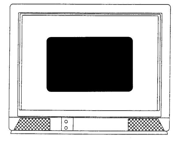
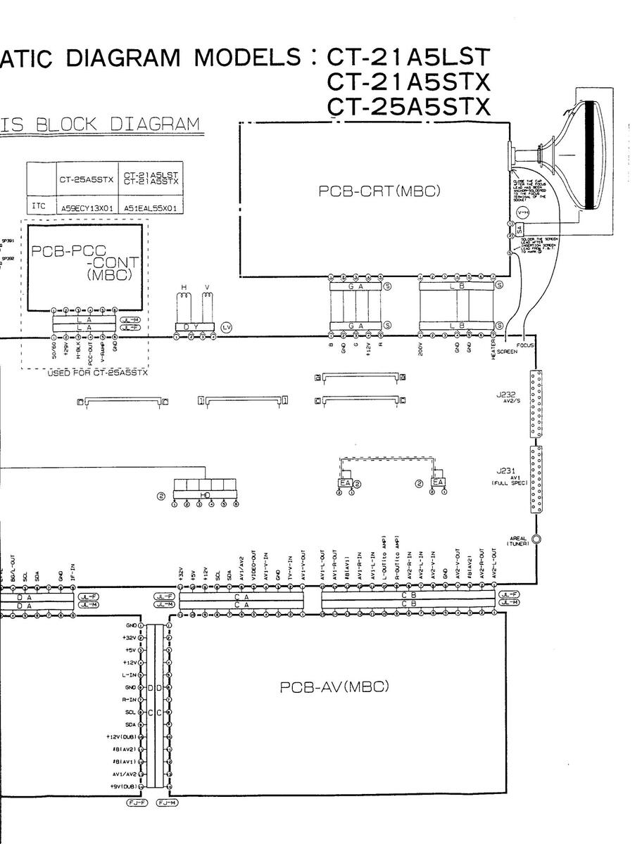
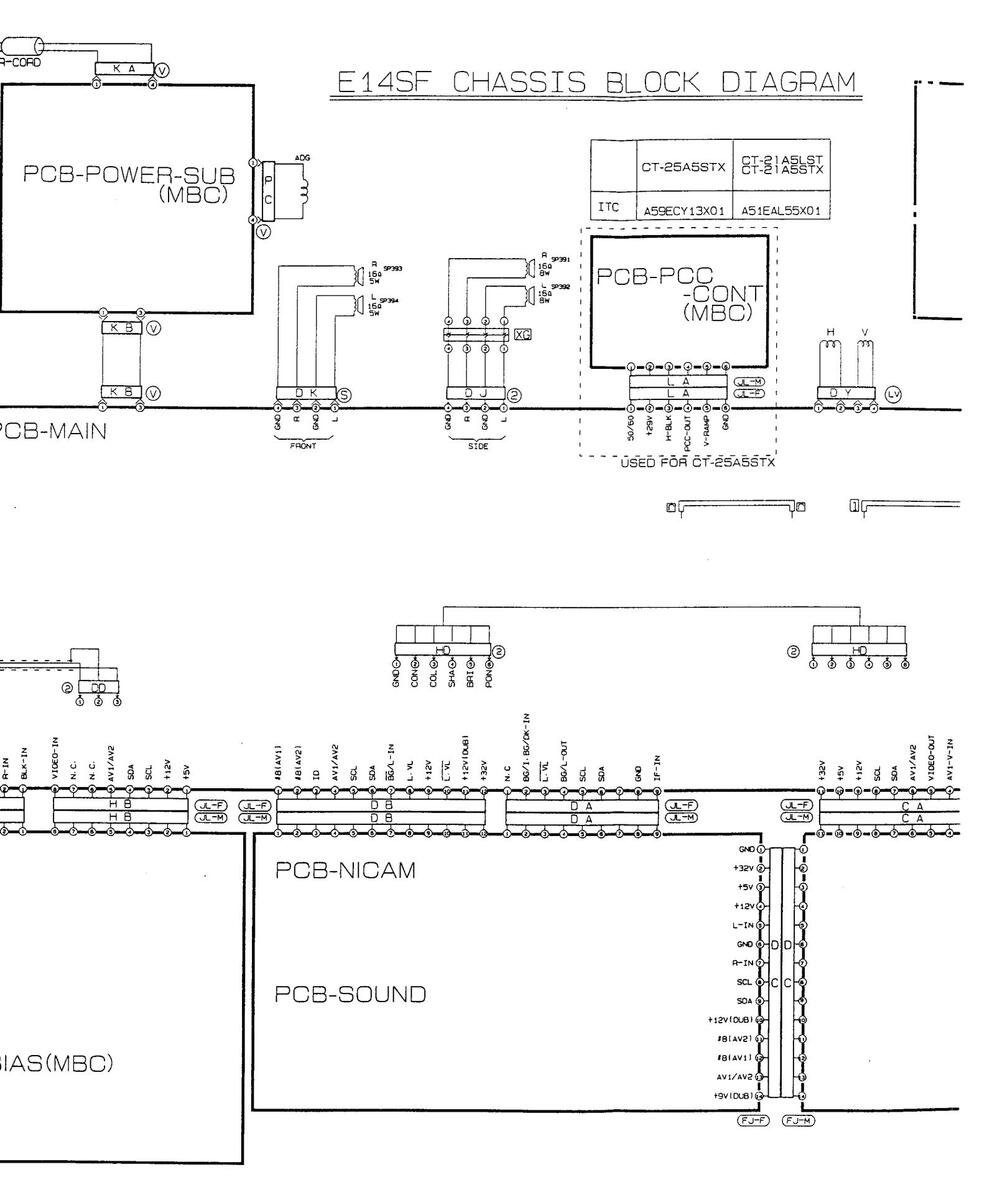
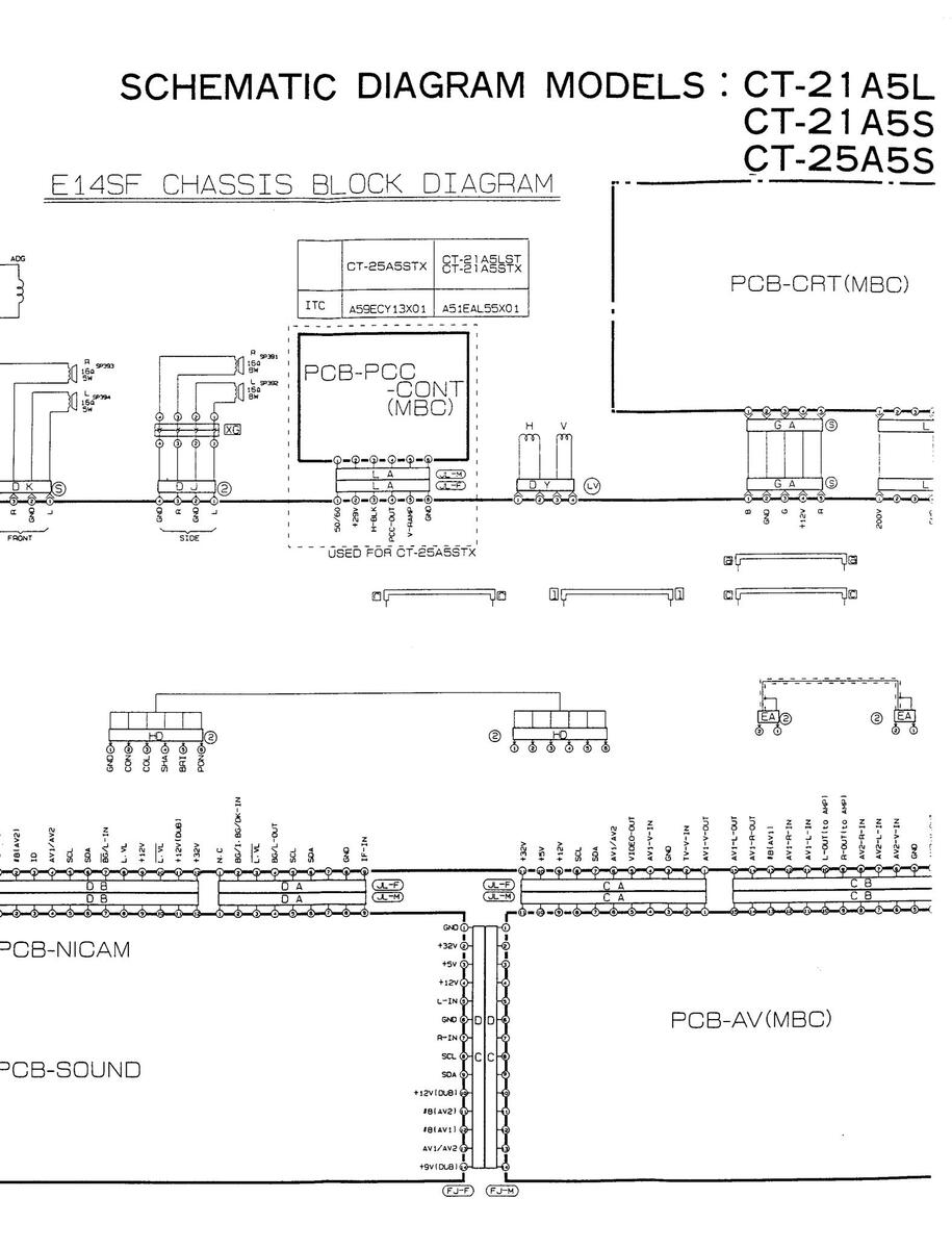
MODEL CT-21A5LST CT-21A5STX CT-25A5STX
CAUTION
Before servicing this chassis, it is important that the serviceman reads the "SAFETY PRECAUTIONS" in this service manual.
SPECIFICATION
| Power Input | AC 230V; 50Hz [CT-21A5LST] |
• Chassis
• Picture tube |
E14SF
A51EAL55X01 |
|---|---|---|---|
|
88W [CT-21A5LST/STX]
97W [CT-25A5STX] |
21″ 90° Deflection [21″ mode1]
A59ECY13X01 |
|
| Reception | CCIR-I | 25" 110° Deflection [25" model] | |
| System |
|
26.5kV (at 1.0mA) | |
|
PAL, 60PAL | voltage | |
| Reception |
VHF 44.5~60.5MHz, 174~214MHz
[CT-21A5LST] UHF 470~870MHz CATV 68~89MHz, 104~470MHz [CT-21A5LST] |
• Cabinet
Dimensions • Weight(Approx.) |
495(W)×447(H)×485(D)mm
[CT-21A5LST/STX] 572(W)×505(H)×442(D)mm [CT-25A5STX] 21.9kg [CT-21A5LST/STX] |
|
Video IF Carrier 39.5MHz
Sound IF Carrier 33.5MHz |
26.2kg [CT-25A5STX] | |
| Aerial Input | 75Ω | ||
| Speaker | 100mm Round type 2pcs |
MITSUBISHI ELECTRIC
Copyright © 1993 Mitsubishi Electric Corporation All Rights Reserved.
CONTENTS
| SAFETY PRECAUTIONS | 1 |
|---|---|
| CONTROLS AND CABINET PARTS | 2 |
| LEAD DRESS | 3 |
| LEAD CONNECTOR COLOUR CODE | 4 |
| FI FCTBICAL ADJUSTMENTS | 5 |
| LOCATION OF TESTPOINTS AND ADJUSTMENT | 6 |
| Audio Circuit Adjustment | _ |
| 1. VCO Coil Adjustment | 7 |
| 2. Audio Deflection Coil Adjustment | 1 |
| VIF Circuit Adjustment | 0 |
| 3. RF AGC Adjustment | 0 |
| Power Circuit Adjustment | Q |
| 4. B4 Voltage Adjustment | 0 |
| CRT Circuit Adjustment | ۵ |
| 5. Cut off, White Adjustment | 10 |
| 6. Focus Adjustment | 10 |
| 7. Black Level Adjustment | 10 |
| Deflection Circuit Adjustment | 11 |
| 8. Horizontal Centre Adjustment | 11 |
| 9. East West PCC Adjustment (25" model only) | 12 |
| 10. Horizontal Width Adjustment (25" model only) | 12 |
| 11. Vertical Height, Vertical Linearity, Vertical Centre Adjustment | 12 |
| Video Circuit Adjustment | 12 |
| 12. Sub Cont Adjustment | 13 |
| PARTS LIST | 14 |
CIRCUIT DIAGRAM
SAFETY PRECAUTIONS
. 1
NOTICE: Observe all cautions and safety related notes located inside the receiver cabinet and on the receiver chassis.
WARNING
- 1. An isolation transformer should be used between the television receiver and the AC supply point before any test/service is performed on a LIVE chassis television receiver.
- Operation of these receivers outside the cabinet or with the cover removed, involves a shock hazard from the receiver power supplies. Work on the receiver should not be attempted by anyone who is not thoroughly familiar with precautions necessary when working on high voltage equipment.
- Do not install, remove or handle the picture tube in any manner unless shatter-proof goggles are worn. People not so equipped should be kept away while the picture tube is being handled. Keep the picture tube away from the body while handling.
- When service is required, observe the original lead dressing. Extra precaution should be given to assure correct lead dressing in the high voltage area. Where a short-circuit has occurred, replace those components that indicate evidence of overheating.
X-RADIATION WARNING
The surface of the cathode ray tube may generate X-Radiation. Precaution during service and, if possible, the use of a lead apron is recommended for shielding while handling.
When replacing the cathode ray tube use only the designated replacement part since it is a critical component with regard to X-Radiation as noted above(No high-voltage adjustments are provided). The high-voltage specification is described on cover page.
LEAKAGE CURRENT COLD CHECK
Before returning the receiver to the customer, it is recommended that leakage current be measured according to the following methods.
With the AC plug removed from the AC source, place a jumper across the live and neutral prongs of the main plug. Turn the receiver AC switch on. Using an 500V D.C Insulation Tester, connect one lead to the jumpered AC plug and touch the other lead to each exposed metal part (antennas, screwheads, etc.), particularly any exposed metal part having a return path to the chassis. Exposed metal parts having a return path to the chassis should have a minimum resistance reading of 4 meg ohm. Any resistance below this value indicates an abnormality which requires corrective action.
CONTROLS AND CABINET PARTS
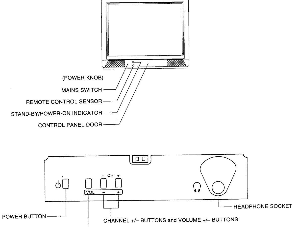
— CHANNEL MODE ↔ VOLUME MODE SELECTOR BUTTON
SCARTS SOCKET CONNECTORS
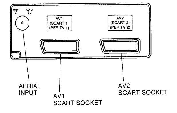
| AV1 | AV2 | AV1 | AV2 | ||||
|---|---|---|---|---|---|---|---|
| 1 | AUDIO | OUTR | 12 | NOT CONNECTED | |||
| 2 | AUDIO | DINR | 13 | RED EARTH | NOT CONNECTED | ||
| 3 | AUDIO | OUT L | 14 | BLANKING EARTH | NOT CONNECTED | ||
| 4 | AUDIO | EARTH | 15 | RED IN | NOT CONNECTED | ||
| 5 | BLUE EARTH | NOT CONNECTED | 16 | RGB STATUS | NOT CONNECTED | ||
| 6 | AUDIO | DINL | 10 | (BLANKING) | |||
| 7 | BLUE IN | NOT CONNECTED | 17 | VIDEO | EARTH | ||
| 8 | FUNCTIO | N SWITCH | 18 | N EARTH | |||
| 9 | GREEN EARTH | NOT CONNECTED | 19 | VIDEO OUT | |||
| 10 | NOT CO | NNECTED | 20 | VIDE | O IN | ||
| 11 | GREEN IN | NOT CONNECTED | 21 | SOCKET EARTH | |||
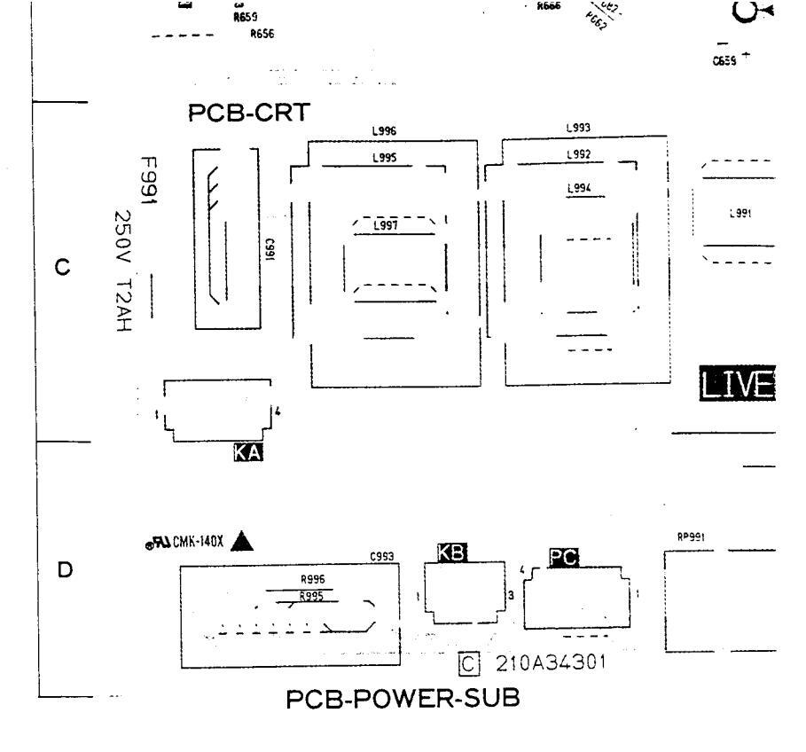
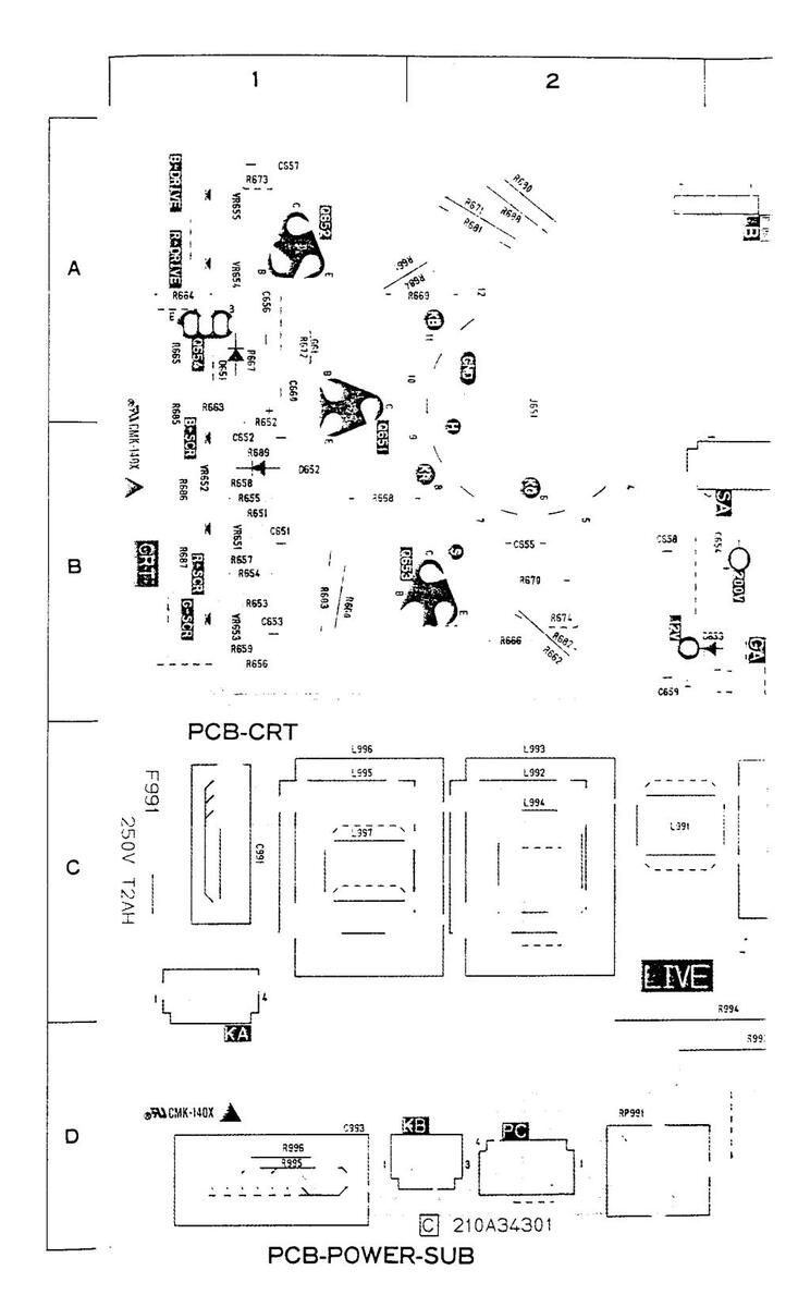
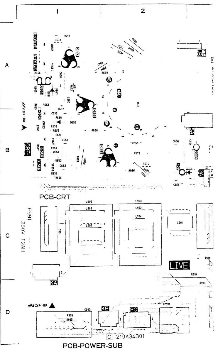
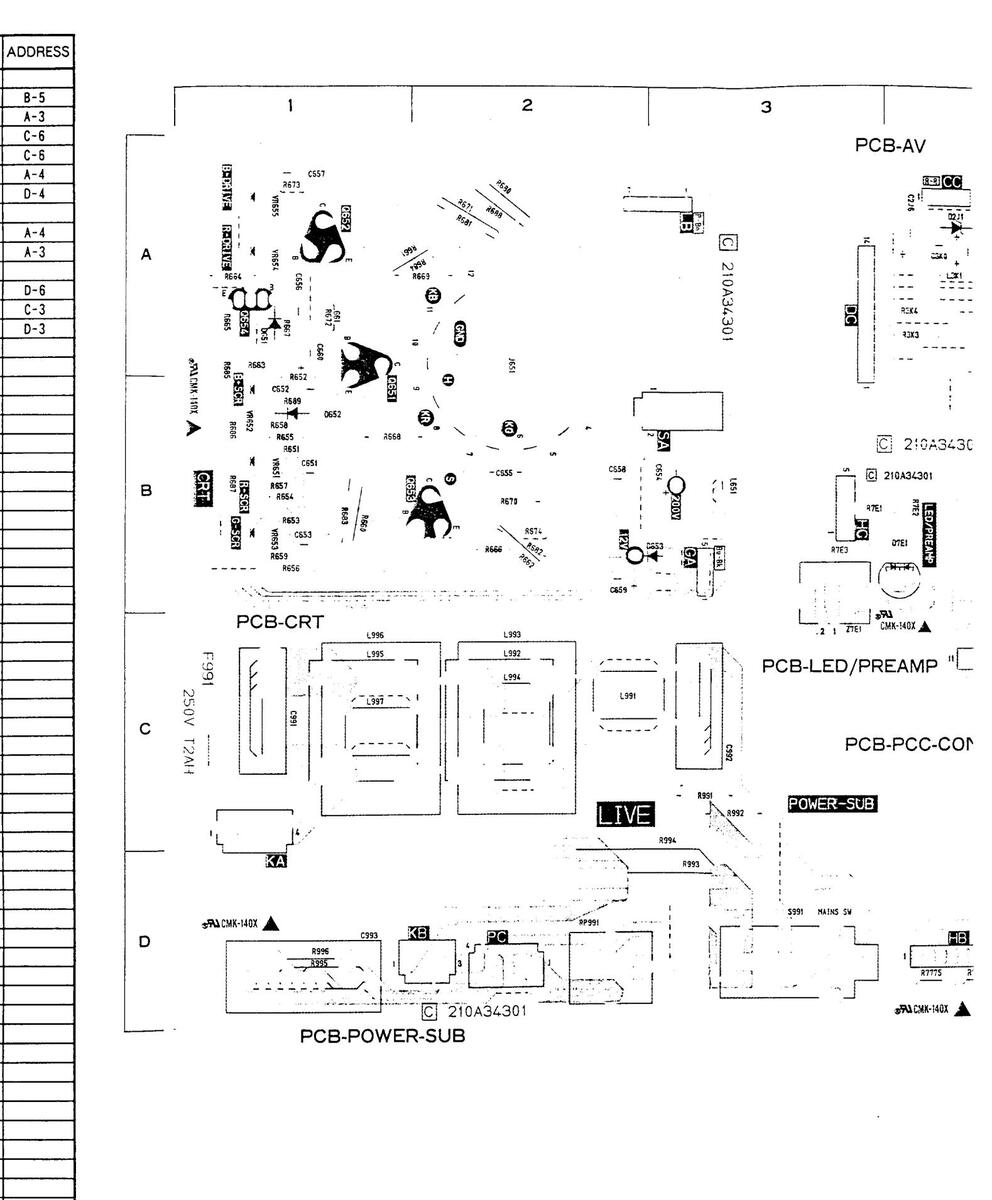
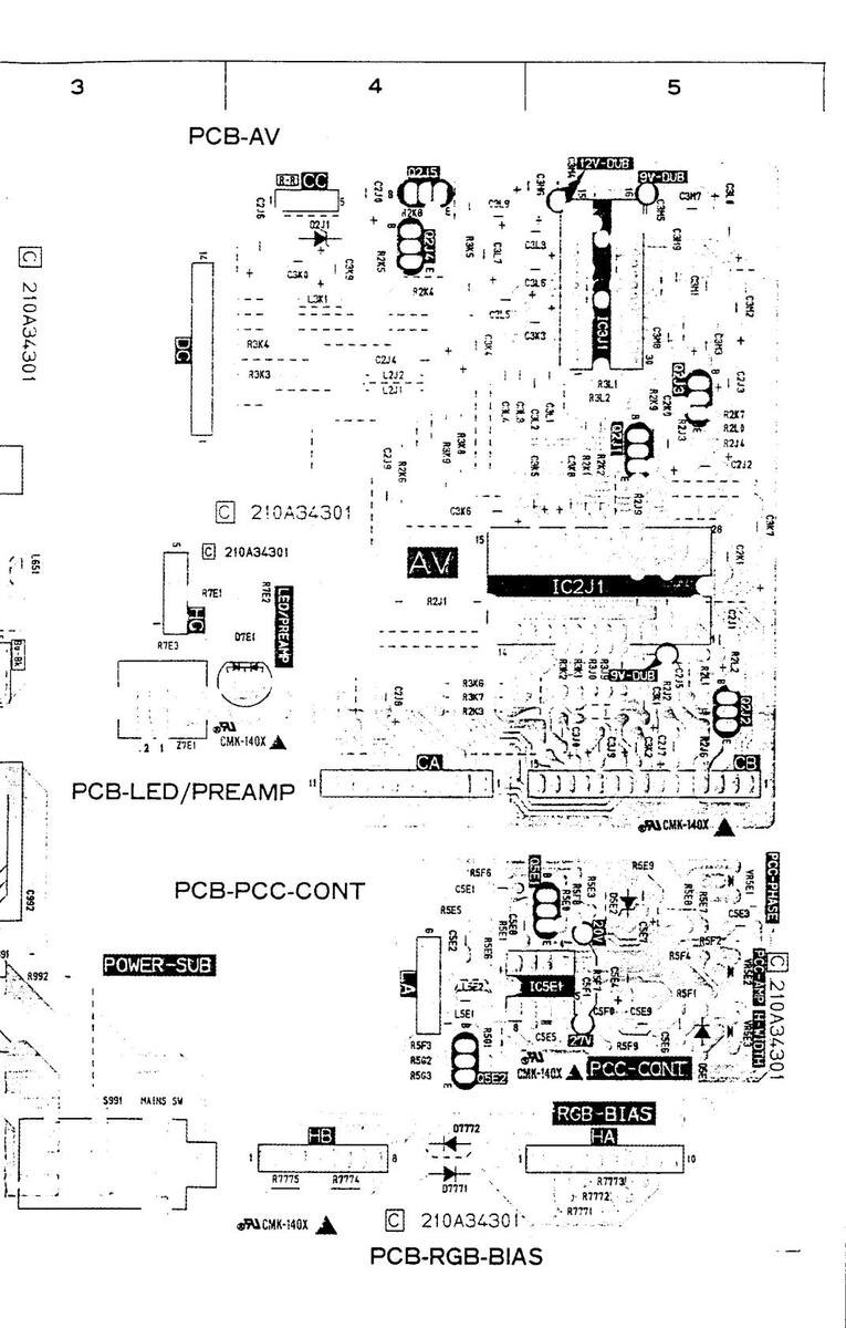
LEAD DRESS
C
ſ
C
The lead wires clamped are listed in the table below.
Note: The inner wires are clamped so that they do not come close to the heat generating or high-tension parts. After servicing route all wires in their original position.
The anode lead wires are routed so no tensile sterngth is applied to the anode cap. If the mounting angle of the anode cap and the route of the anode lead wires are changed. Return them to the initial angle and route.
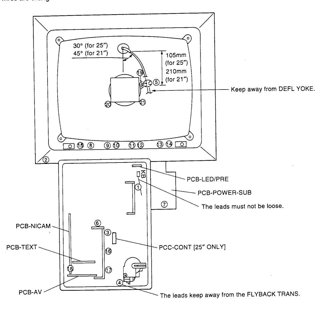
| CLAMPER LIST FOR | CONNECTOR | LEAD |
|---|
| CLANP | |
|---|---|
| CONNECTOR LEAD | |
| ANODE-LEAD | (5) must be held by (19) |
| DD | 6 |
| DJ-SP393 | ② - 15 - ⑧ - ⑨ - ① - ① - ② (21" only)- ④ |
| DJ-SP394 | 2 |
| DK | ② (Loop DK to take up slack) |
| DY | ③ (1 loop)- ④- ⑦ |
| FOCUS-LEAD | ④- ② |
| GA | 6-6-00 |
| КВ | 1 |
| LB | |
| PC | ⑦ (1 loop 21" only)- ① |
| SA | 16 · 1 |
| SCREEN LEAD | Q.21 |
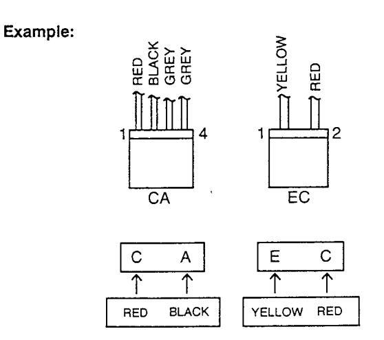
LEAD CONNECTOR COLOUR CODE
Lead connectors show the connector names by colour codes of leads, not printed any connector names. When connecting or removing them, identify connector names according to colour codes in the table below. Colour Codes (See Pin Nos. 1 and 2 of connectors)
| Colour | Code |
|---|---|
| BLACK | А |
| BROWN | В |
| RED | С |
| ORANGE | D |
| YELLOW | E |
| GREEN | NOT USED (GROUND) |
| BLUE | G |
| VIOLET | Н |
| GREY | J |
| WHITE | к |
| PINK | Ł |
C
WHEN SERVICING PCB USE THE EXTENSION CORD
| PRINTED CIRCUIT BOARD | CONNECTOR | PARTS NO. |
|---|---|---|
|
AV
NICAM TEXT LED/PRE |
CB (15pin)
DA (9pin), DB (12pin) HB (8pin) HC (5pin) |
859C431O40 |
| PCC-CONT (only 25") | LA (6pin) | 859C431O60 |
| AV | CA (11pin) | 859C432O40 |
| TEXT | HA (10pin) | 859C432O80 |
ELECTRICAL ADJUSTMENT
Perform only the alignments required. If proper equipment is not available, do not attempt an alignment.
Measuring equipment and Jigs
- Oscilloscope (Unless otherwise specified in particular, use 10:1 probes.)
- Signal generator
- Direct current milliammeter
- Direct current voltmeter.
- Electrical tools
Test Signal
1) Monoscope signal
When you have no monoscope signal source for adjustment, connect the unit to a VCR and play an alignment tape (Monoscope).
2) Colour bar signal
In this manual, unless otherwise specified in particular, use colour bar signal in specifications below.
Split-Field Colour Bars (with 100% window)
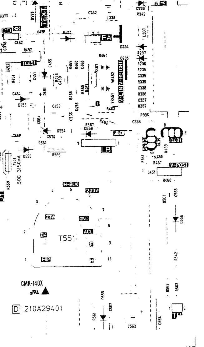
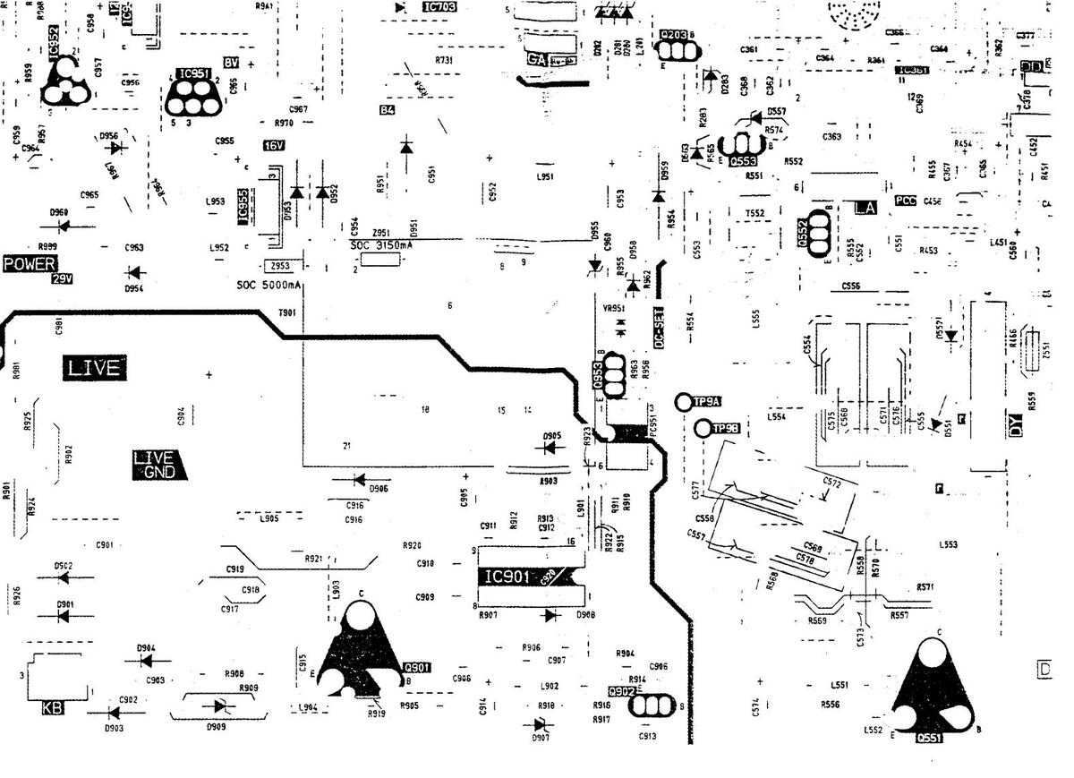
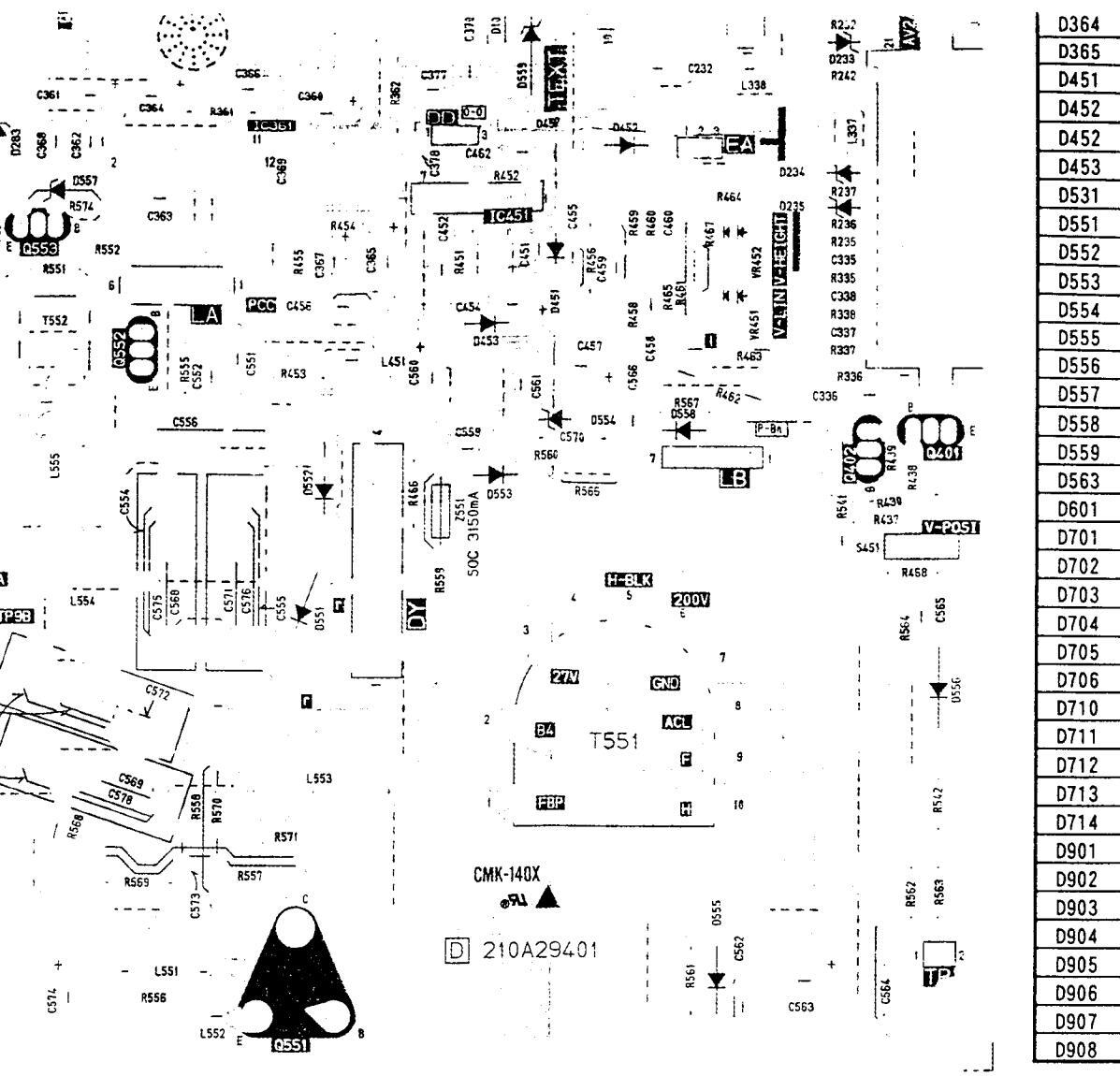
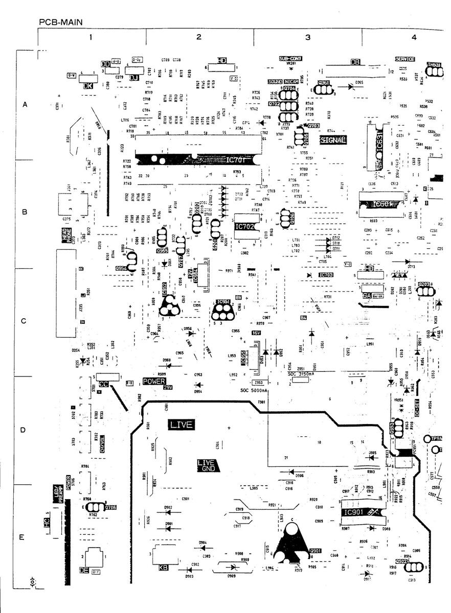
LOCATION OF TESTPOINTS AND ADJUSTMENTS
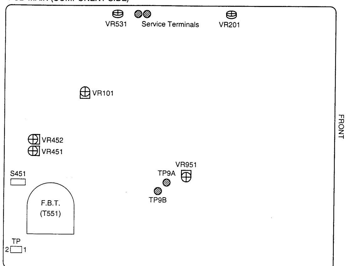
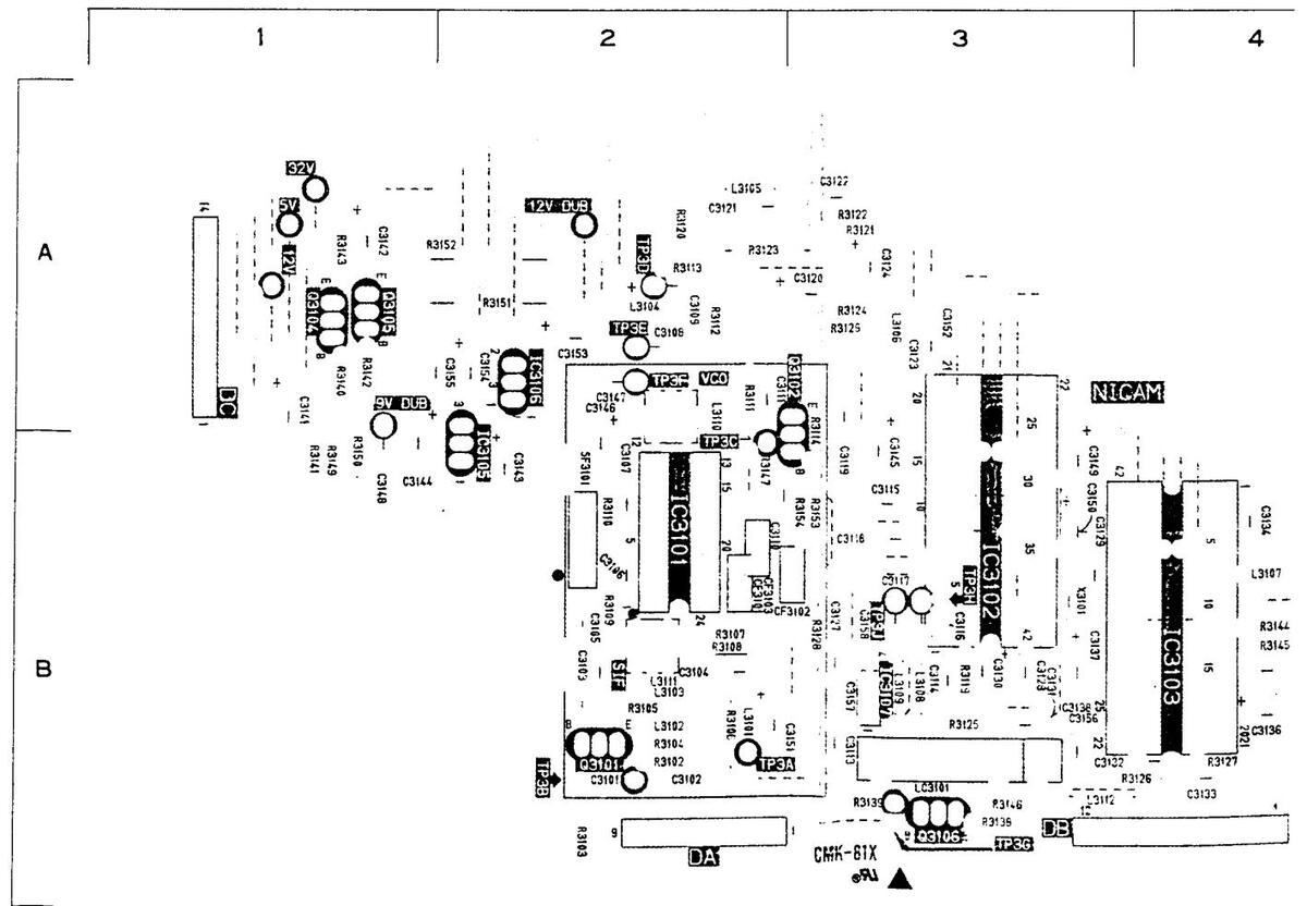
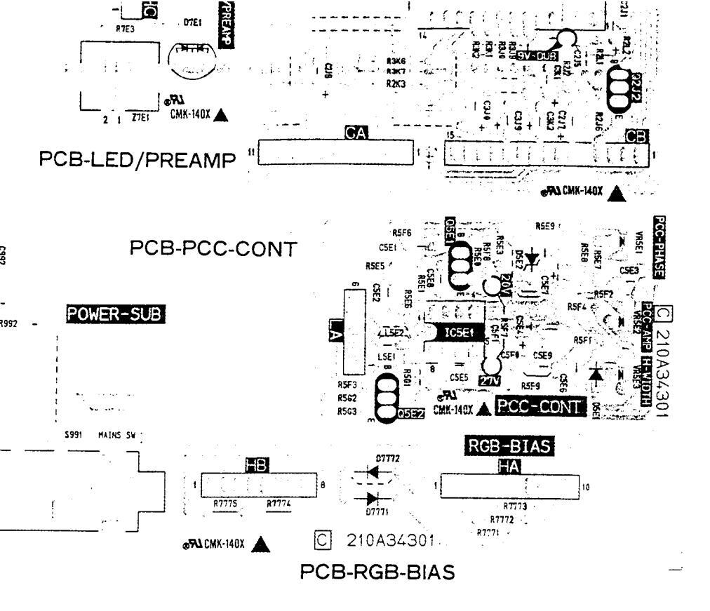
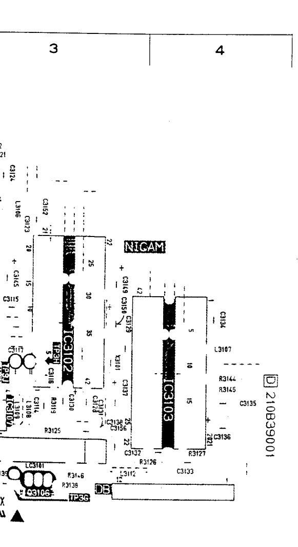
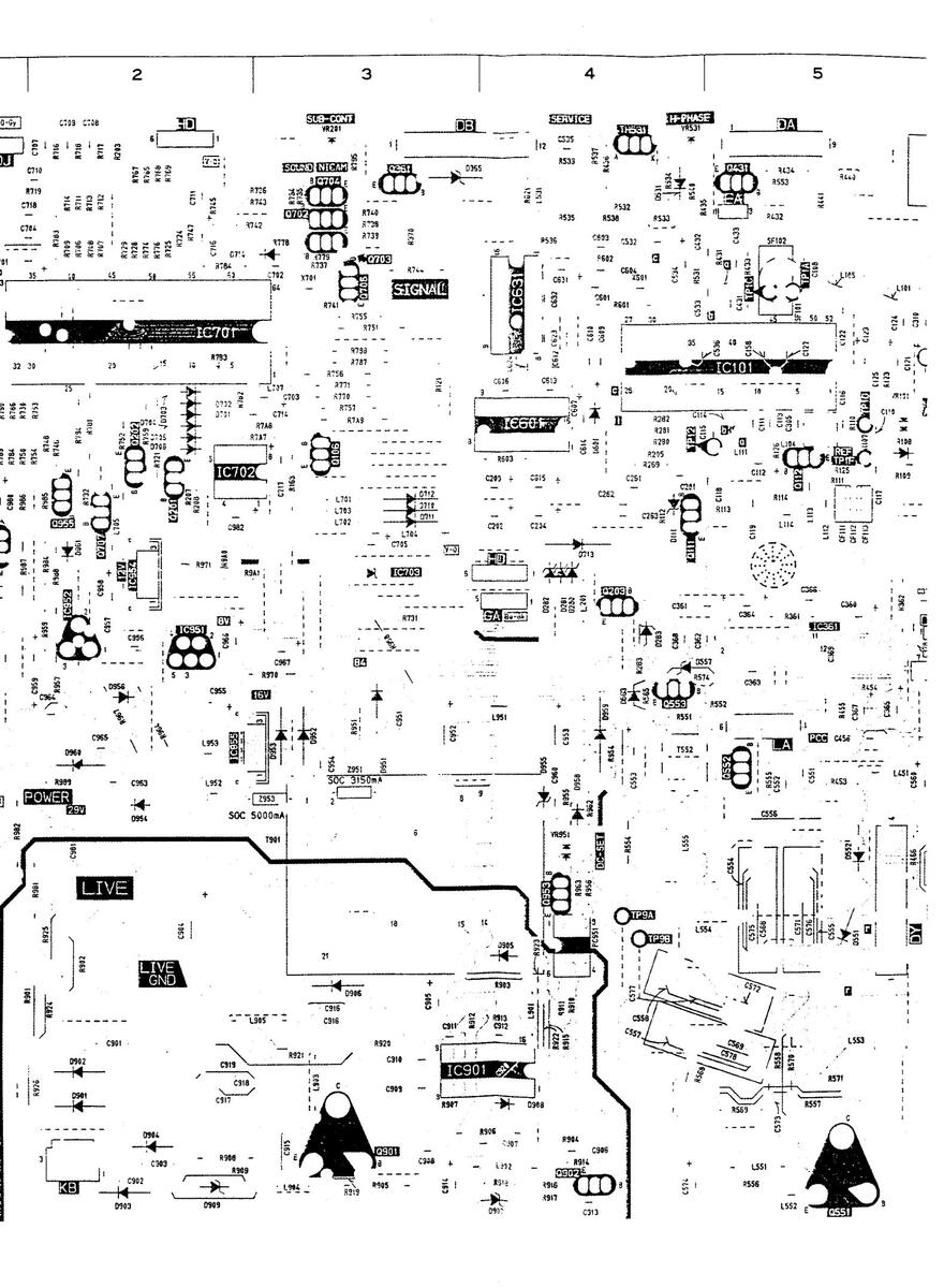
PCB-MAIN (COMPONENT SIDE)
ſ
- 7 -
| [VIF circuit] | Adjustment purpose The best receiving condition of RF signal. | |
|---|---|---|
| 3. HF AGC | Symptom when Poor S/N ratio or cross modulation. | |
| Measuring | 1. Supply an RF signal(Programme). | |
|
||
|
EX I trigger
Measurement |
||
| range | ||
| Input signal |
R⊢ signal
(Programme) |
|
| Input terminal | RF IN termina | al |
| PCB-MAIN (COM | PONENT SIDE) | FRONT |
|
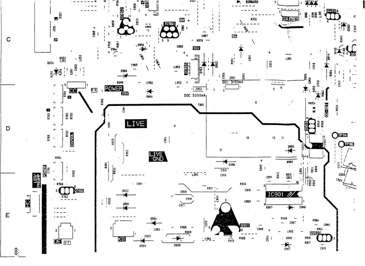
[Power circuit
4. B4 Voltage Measuring instrument |
]
DC Voltmeter |
Adjustment purpose The best value of power supply voltage for horizontal deflection circuit. Symptom when incorrectly adjusted Too bright or too dark picture. Too compressed or too expanded horizontal width of picture. 1. Supply an RF signal (Programme). 2. Observe the voltage at TP9A and TP9B (Plus lead to TP9A). |
| Test point |
+ lead : TP9A
- lead : TP9B |
3. Adjust VR951 so that the voltage is a value listed in the table below. |
| EXT trigger | 21 inch 25 inch | |
|
leasurement
ange |
Voltage Value 122 ± 3V 145 ± 1V | |
| nput signal |
RF signal
(Programme) |
|
| nput terminal | RF IN terminal | |
| PCB-MAIN (COMF | PONENT SIDE) | |
|
Symptom when
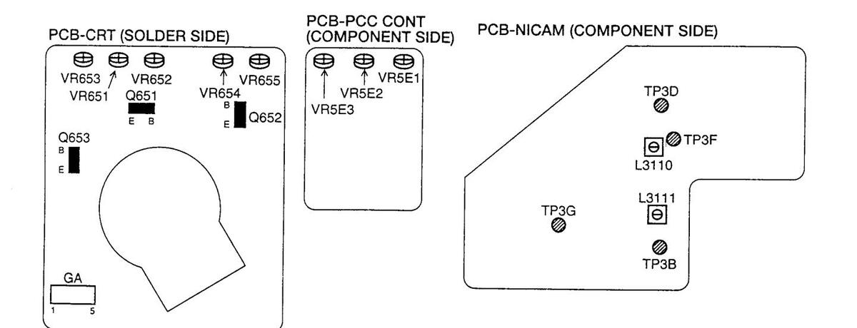
instrument Symptom when instrument Too dark or too bright picture. Incorrectly adjusted Measuring instrument Oacilloscope * This adjustment must follow the Purity and Convergence adjustments. * Adjustrument lenn 12 (buc Conf) must be performed immediately after this one. 1. Set the no signal condition in AV mode. EXT trigger * Adjustrument lenn 12 (buc Conf) must be performed immediately after this one. 2. Set VR65, VR655 and VR201 to the mechanical centre position. 2. Set VR65, VR655 and VR201 to the mechanical centre position. 3. Closence the waveform at the collector of Q651.(Use GA connector pin (2) for ground). Measurement DIV FV angge input terminal |
[CRT circuit] | ite | Adjustment p | urpose | Rate of electron beam shot from each electron gun of R, G and |
|---|---|---|---|---|---|
|
Measuring
instrument instrument instrument instrument instrument instrument input signal
|
5. Out Oil, Wil | Symptom who incorrectly ac |
en
ljusted |
Too dark or too bright picture. | |
| Test point collector of Q651 1 4 Adjustment Item 12 (Sub Cont) must be performed immediately after this one. 1 Set VR651, VR652 and VR653 to the mechanical centre position. 2 Set VR654, VR655 and VR201 to the mechanical centre position. 3 Set VR654, VR655 and VR201 to the mechanical centre position. 4 Observe the waveform at the collector of Q651,(Use GA connector pin (2) for ground). 5 Adjust VR651 so that the pedestal level is 150V. 100 Serve the waveform at the collector of Q652,(Use GA connector pin (2) for ground). 6 Observe the waveform at the collector of Q653,(Use GA connector pin (2) for ground). 7 Adjust VR653 so that the pedestal level is 150V. 8 Observe the waveform at the collector of Q653,(Use GA connector pin (2) for ground). 8 Observe the waveform at the collector of Q653,(Use GA connector pin (2) for ground). 9 Observe the waveform at the collector of Q653,(Use GA connector pin (2) for ground). 10 Short - circut the service terminals. 11 Adjust VR651, VR652 and VR653 so that the horizontal line is white. 10 Short - circut the service terminals. 11 Adjust VR654, and VR653 so that the entire screen is pure white. 12 Adjust VR654 and V |
Measuring
instrument |
Oscilloscope |
* This
* Prel |
adjustme |
ent must follow the Purity and Convergence adjustments.
et for twenty minutes or more. |
| EXT trigger | Test point | collector of C |
* Adju
2651 1. Set 2. Set |
ustment Ite
the no sig VB651, V |
em 12 (Sub Cont) must be performed immediately after this one.
nal condition in AV mode. R652 and VR653 to the mechanical centre position. |
|
Measurement
Input signal DIV 5V TIM 20µs Input signal |
EXT trigger |
3. Set
4. Obs |
VR654, V
erve the v |
R655 and VR201 to the mechanical centre position.
vaveform at the collector of Q651.(Use GA connector pin 2) for |
|
| Input signal |
Measurement
range |
DIV 5V
TIM 20μs |
grou
5. Adju |
und.)
ust VR651 |
so that the pedestal level is 150V. |
| Input terminal | Input signal | 150V | pedestal level | ||
|
Input terminal | ٥V | |||
| ground.) 9. Adjust VR653 so that the pedestal level is 150V. 9. Adjust VR653 so that the pedestal level is 150V. 9. Adjust VR653 so that the pedestal level is 150V. 9. Become super state s | PCB-MAIN (COM |
PONENT SIDE)
• |
6. Ob:
gro 7. Adj 8. Ob: |
serve the
und.) ust VR652 serve the |
waveform at the collector of Q652.(Use GA connector pin ② for 2 so that the pedestal level is 150V.
waveform at the collector of Q653.(Use GA connector pin ② for |
|
B. OD:
gro |
und.) | waveform at the collector of Q655.(Use GA connector pin @ for | ||
| PCB-CRT (SO |
LDER SIDE)
552 ↑ VR655 1 VR654 e e E Q0652 |
10. Sł
11. Ac lin 12. Ac 13. Oj 14. Su 15. Ac |
hort - circu
djust SCRI e become djust two o ben the se upply a vid djust VR65 |
t the service terminals.
EEN control on F.B.T. to the point where one red, green or blue is just visible. If VR651, VR652 and VR653 so that the horizontal line is white. ervice terminals. leo signal (White raster). 54 and VR 655 so that the entire screen is pure white. |
|
|
GA
GA |
· | · | |||
Ç.
| 6. Focus | Adjustment purpose Sharpness of picture. | ||
|---|---|---|---|
| Symptom when Poor sharpness of picture. | |||
|
Measuring
instrument |
Supply an RF signal(Programme). Adjust FOCUS volume on F.B.T. to the best overall focus. | ||
| Test point | |||
| EXT trigger | |||
| Measurement range | |||
| Input signal |
RF signal
(Programme) |
||
| Input terminal | RF IN termina | ||
| PCB-MAIN (COM | PONENT SIDE) | FRONT | C |
| 7 Black Level | E | ||
| Symptom when Too bright or too dark picture. | • | ||
|
Measuring
instrument |
|
||
| Test point |
3. Make sure that the blue bar area does not brighten.
If necessary, adjust SCREEN control on FBT so that the blue bar area does |
||
| EXT trigger |
|
ſ | |
| Measurement range | * | slightly bright. | |
| Input signal |
Video signal
(Colour bar) |
||
| Input terminal | VIDEO IN term | inal | |
| PCB-MAIN (CC | OMPONENT SI | DE) | ( |
|
Measuring
instrument Test point EXT trigger |
_ | ||||
|---|---|---|---|---|---|
|
Measuring
instrument - Test point - EXT trigger - |
Sympto
incorre |
om when Picture too shifted to the left, or the right. | |||
|
Test point -
EXT trigger - |
|
eo signal (Monoscope).
I so that readings of left and right markers are the same. |
|||
| EXT trigger - | |||||
|
measurement
range |
right marker | ||||
| Input signal ( |
Video signal
(Monoscope) |
le | eft marker | ||
| Input terminal | VIDEO IN terr | minal | |||
| 9. East West PC | Adjust | nent purpose | |||
| (25" model only) | 0 | Sympto | nonzonial linearity of picture. | ||
| ( moder orny) | om when | Horizontal distortion of picture | |||
| Measuring | incorre |
om when
ctly adjusted |
Horizontal distortion of picture. | ||
|
Measuring
instrument |
om wnen
ctly adjusted 1. Supply a vide 2. Press OPTIM 3 Observing the |
Horizontal distortion of picture.
o signal (Crosshatch). UM button on the remote hand unit. |
|||
|
Measuring
instrument Test point |
om wnen
ctly adjusted 1. Supply a vide 2. Press OPTIM 3 Observing the Adjust VR5E1 4. Adjust VR5E2 |
Horizontal distortion of picture.
o signal (Crosshatch). UM button on the remote hand unit. e second line from both ends on the screen. so that the upper and lower distortions are symmetrical. t so that the both vertical lines are straight. |
|||
|
Measuring
instrument |
|
Horizontal distortion of picture.
o signal (Crosshatch). UM button on the remote hand unit. e second line from both ends on the screen. so that the upper and lower distortions are symmetrical. to that the both vertical lines are straight. to 4 above, if necessarly. |
|||
|
Measuring
instrument |
|
Horizontal distortion of picture.
o signal (Crosshatch). UM button on the remote hand unit. e second line from both ends on the screen. so that the upper and lower distortions are symmetrical. e so that the both vertical lines are straight. to 4 above, if necessarly. |
|||
|
Measuring
instrument Test point EXT trigger Measurement range V input signal V |
/ideo signal Crosshatch) |
om when
ctly adjusted 1. Supply a vide 2. Press OPTIM 3 Observing the Adjust VR5E1 4. Adjust VR5E2 Repeat step 3 |
Horizontal distortion of picture.
o signal (Crosshatch). UM button on the remote hand unit. e second line from both ends on the screen. so that the upper and lower distortions are symmetrical. so that the both vertical lines are straight. to 4 above, if necessarly. |
||
| [Video circuit] Adjust | tment purpose | The best va | alue of beam cur | rent. | |||||
|---|---|---|---|---|---|---|---|---|---|
|
Symp
Symp |
tom when
ectly adjusted |
Too bright o | or too dark pictur | е. | |||||
|
Measuring
instrument |
DC milliamm | neter |
|
et for twenty
o signal (Col |
minutes or more
our bar). |
- | |||
| Test point |
+lead :TPconne
-lead :TPconne |
ctor pin①
ctor pin② |
|
||||||
| EXT trigger | |||||||||
| Measurement range | ····· | ٦ | |||||||
| Input signal | Video signal | 21 inch | 25 inch | ||||||
| Bea | am Current | 875±20µА | 1030±20μA | ||||||
| PCB-MAIN (COM | 01 | ||||||||
| FHO | |||||||||
| ā | |||||||||
| i. | |||||||||
- 13 -
PARTS LIST
MODEL : CT-21A5LST/CT-21A5STX/CT-25A5STX
In order to expedite delivery of replacement part orders.
Specify : 1.Model number/Serial number
2.Part number and Description
3.Quantity
Unless full information is supplied, delay in execution of orders will result.
▲ : Critical components
| MARK | В | С | D | F | G | J | к |
|---|---|---|---|---|---|---|---|
|
TOLERANCE
(%) |
±0.1 | ±0.25 | ±0.5 | ±1 | ±2 | ±5 | ±10 |
| MARK | М | Ν | V | Х | Ζ | Ρ | Q |
|---|---|---|---|---|---|---|---|
|
TOLERANCE
(%) |
±20 | ±30 |
+10
-10 |
+40
-20 |
+80
-20 |
+100
-0 |
+30
-10 |
| MARK | В | С | D | F | G |
|---|---|---|---|---|---|
|
TOLERANCE
(pF) |
±0.1 | ±0.25 | ±0.5 | ±1 | ±2 |
ABBREVIATION [21LST]:CT-21A5LST [21STX]:CT-21A5STX [25STX]:CT-25A5STX
[21LST]:CT-21A5LST [21STX]:CT-21A5STX [25STX]:CT-25A5STX
|
SYMBOL PARTS PARTS NAME
No. No. PARTS NAME |
DESCRIPTION |
SYMBOL PARTS PARTS NAME
No. No. PARTS NAME |
DESCRIPTION | |
|---|---|---|---|---|
| TURES | Q 5E2 260P543O30 TRANSISTOR | JC501-R[25STX] | ||
|
▲ V 271 255P801O10 CRT ASSY
▲ V 271 255P930O10 CRT ASSY INTEGRATED CIRCUITS |
A51EAL55X01[21LST,21STX]
A59ECY13X01[25STX] |
Q 651 260P571010 TRANSISTOR
Q 652 260P571010 TRANSISTOR Q 653 260P571010 TRANSISTOR Q 654 260P544040 TRANSISTOR Q 702 260P544040 TRANSISTOR |
2SC3789-D,E
2SC3789-D,E 2SC3789-D,E JA101-R JA101-R |
|
| IC101 272P847O20 IC IC2J1 272P575O10 IC IC361 272P459O20 IC IC3J1 272P942O10 IC IC3101 270P068O10 IC |
TDA8361
CXA1114P TA8200AH TA8776N LA7555 |
Q 703 260P544O40 TRANSISTOR
Q 704 260P544O40 TRANSISTOR Q 705 260P543O30 TRANSISTOR Q 706 260P543O30 TRANSISTOR Q 707 260P543O30 TRANSISTOR |
JA101-R
JA101-R JC501-R JC501-R JC501-R |
|
| IC3102 274P340010 IC IC3103 274P339010 IC IC3105 272P785010 IC IC3106 266P922020 IC IC3107 266P982010 IC |
TDA8205
TDA8204 μPC78M09AHF μPC78M05H AN608P |
Q 7701 260P543O30 TRANSISTOR
Q 7702 260P543O30 TRANSISTOR Q 7703 260P543O30 TRANSISTOR Q 7707 260P543O30 TRANSISTOR Q 901 260P572O10 TRANSISTOR |
JC501-R
JC501-R JC501-R JC501-R 2SD1556 |
|
|
₩
19 |
IC451 266P405O10 IC IC5E1 272P406O10 IC IC601 272P848O10 IC IC701 274P336O10 IC IC702 263P434O20 IC |
AN5521
TEA2031A[25STX] TDA4661 P83CL168 X24C04P |
Q 902 260P543O30 TRANSISTOR Q 953 260P543O30 TRANSISTOR Q 954 260P668O10 TRANSISTOR Q 955 260P325O30 TRANSISTOR Q 975 260P544O40 TRANSISTOR |
JC501-R
JC501-R 2SB1135-R,S 2SC2655-Y JA101-R |
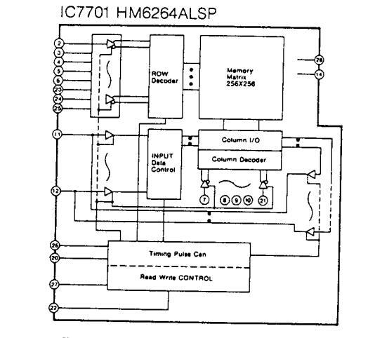
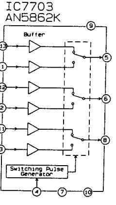
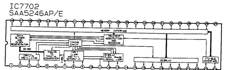
| IC703 266P010020 IC IC7701 263P622020 IC IC7702 274P050020 IC IC7703 272P027010 IC IC7704 272P400010 IC IC901 272P514010 IC |
μPC574J-K
HM6264ALSP10/12 SAA5246AP AN5862K NJM2233BL TEA2261 |
DIODES
D 102 264P370010 DIODE D 231 264P483080 DIODE D 232 264P483080 DIODE D 233 264P483080 DIODE D 233 264P483080 DIODE |
1N4148
RD5.1FB2 RD5.1FB2 RD5.1FB2 RD5.1FB2 |
|
|
IC951 267P076O10 IC
IC952 266P922O10 IC IC954 272P856O10 IC IC955 272P502O10 IC TBANSISTORS |
SI-3120C
μPC78M05H μPC78M08AHF μPC2412HF |
D 235 264P483080 DIODE
D 251 264P483080 DIODE D 252 264P483080 DIODE D 252 264P483080 DIODE D 253 264P483080 DIODE D 253 264P483080 DIODE |
RD5.1FB2
RD5.1FB2 RD5.1FB2 RD5.1FB2 RD5.1FB2 RD5.1FB2 |
|
| Q 111 260P543O30 TRANSISTOR Q 112 260P543O30 TRANSISTOR Q 201 260P543O30 TRANSISTOR Q 202 260P543O30 TRANSISTOR Q 202 260P543O30 TRANSISTOR Q 203 260P544O40 TRANSISTOR |
JC501-R
JC501-R JC501-R JC501-R JA101-R |
D 281 264P462O90 DIODE
D 282 264P462O90 DIODE D 2J1 264P464O30 DIODE D 361 264P370010 DIODE D 362 264P370010 DIODE |
RD7.5EB3
RD7.5EB3 RD10EB2 1N4148 1N4148 |
|
|
Q 261 260P544O40 TRANSISTOR
Q 2J1 260P543O30 TRANSISTOR Q 2J2 260P543O30 TRANSISTOR Q 2J3 260P543O30 TRANSISTOR Q 2J4 260P543O30 TRANSISTOR |
JA101-R
JC501-R JC501-R JC501-R JC501-R |
D 363 264P370010 DIODE D 364 264P370010 DIODE D 365 264P463020 DIODE D 451 264P371010 DIODE D 452 264P371010 DIODE |
1N4148
1N4148 RD8.2EB2 BYD33G BYD33G |
|
| i |
Q 2J5 260P387O30 TRANSISTOR
Q 361 260P544O40 TRANSISTOR Q 3101 260P356O10 TRANSISTOR Q 3102 260P544O40 TRANSISTOR Q 3104 260P543O30 TRANSISTOR |
2SC2236-Y
JA101-R 2SC1906 JA101-R JC501-R |
D 453 264P371O10 DIODE
D 531 264P370O10 DIODE D 551 264P533O30 DIODE D 552 264P358O70 DIODE D 553 264P371O10 DIODE |
BYD33G
1N4148 RS 4FS[25STX] RU 4AM[25STX] BYD33G |
| Q 3105 260P543O30 TRANSISTOR Q 3106 260P543O30 TRANSISTOR Q 401 260P543O30 TRANSISTOR Q 402 260P543O30 TRANSISTOR Q 431 260P543O30 TRANSISTOR Q 431 260P349O20 TRANSISTOR |
JC501-R
JC501-R JC501-R JC501-R ZSC1472K-B[25STX] |
D 554 264P463O20 DIODE
D 555 264P371O10 DIODE D 556 264P371O10 DIODE D 557 264P456O60 DIODE D 557 264P465O10 DIODE |
RD8.2EB2
BYD33G BYD33G RD2.2EB2[21LST,25STX] RD12EB1[21STX] |
|
|
Q 551 260P576O10 TRANSISTOR
Q 551 260P557O10 TRANSISTOR Q 552 260P422O10 TRANSISTOR Q 551 260P543O30 TRANSISTOR |
2SD1554[21LST,21STX]
2SD1555[25STX] 2SC2482 JC501-R[25STX] |
D 558 264P371010 DIODE
D 559 264P463060 DIODE D 563 264P370010 DIODE D 5E1 264P370010 DIODE |
BYD33G
RD9.1EB1 1N4148 1N4148[25STX] |
[21LST]:CT-21A5LST [21STX]:CT-21A5STX [25STX]:CT-25A5STX
| and the second | |||||||
|---|---|---|---|---|---|---|---|
|
YMBOI
No. |
L PARTS PARTS NAM | ME DESCRIPTION |
SYMBC
No. |
DL PARTS
No. |
PARTS NAME | DESCRIPTION | |
| D 5E2 | 264P467080 DIODE | RD20EB3[25STX] | L 114 | 325C162O00 | PEAKING COIL | 39µН-К | 1 |
|
D 601
D 651 D 653 D 701 D 702 |
264P483080 DIODE
264P370010 DIODE 264P371010 DIODE 264P370010 DIODE 264P370010 DIODE |
RD5.1FB2
1N4148 BYD33G 1N4148[21LST] 1N4148[21LST] |
L 151
L 152 L 201 L 2J1 L 2J2 |
325C121O30
325C121O30 325C122O50 325C110O10 325C110O10 |
PEAKING COIL
PEAKING COIL PEAKING COIL PEAKING COIL PEAKING COIL |
10µН-К
10µН-К 100µН-К 1.0µН-К 1.0µН-К |
|
|
D 710
D 711 D 712 D 713 D 714 |
264P370010 DIODE
264P370010 DIODE 264P370010 DIODE 264P370010 DIODE 264P370010 DIODE |
1N4148
1N4148 1N4148 1N4148 1N4148 |
L 3K1
L 3101 L 3102 L 3103 L 3104 |
325C110O10
325C122O30 325C120O40 325C122O30 325C122O30 |
PEAKING COIL
PEAKING COIL PEAKING COIL PEAKING COIL PEAKING COIL |
1.0µН-К
68µН-К 1.8µН-М/К 68µН-К 68µН-К |
|
|
D 7E1
D 7701 D 7702 D 7703 D 7704 |
264P584O20 LIGHT EMITTING DI
264P370010 DIODE 264P370010 DIODE 264P370010 DIODE 264P370010 DIODE 264P370010 DIODE |
IODE SML1216W-C,D
1N4148 1N4148 1N4148 1N4148 1N4148 |
L 3105
L 3106 L 3107 L 3108 L 3109 |
325C121O30
325C121O30 325C121O30 325C113O20 325C113O20 |
PEAKING COIL
PEAKING COIL PEAKING COIL PEAKING COIL PEAKING COIL |
10µН-К
10µН-К 10µН-К 390µН-К 390µН-К |
|
|
D 901
D 902 D 903 D 904 D 905 |
264P376010 DIODE
264P376010 DIODE 264P376010 DIODE 264P376010 DIODE 264P376010 DIODE 264P371010 DIODE |
BYW56
BYW56 BYW56 BYW56 BYD33G |
L 3110
L 3111 L 531 L 532 L 551 |
323P184O10
327P074O10 325C120O10 325C120O10 321C030O10 |
VIF COIL
SIF COIL PEAKING COIL PEAKING COIL RF COIL |
5.5/6.0MHz
1.0µH-M 1.0µH-M 1.0µH-K |
|
|
D 906
D 907 D 908 D 909 D 951 |
264P372O10 DIODE
264P481O60 DIODE 264P370010 DIODE 264P481O60 DIODE 264P358070 DIODE |
BYV96E
RD3.0FB2 1N4148 RD3.0FB2 RU 4AM |
L 552
L 553 L 553 L 554 L 555 |
411D009O20
333P012O30 333P012O10 409P748O10 409P749O10 |
FERRITE CORE FILTER
H-LIN. COIL H-LIN. COIL PCC COIL CHOKE COIL |
[21LST,21STX]
[25STX] 1MHz[25STX] 15MHz[25STX] |
|
|
D 952
D 953 D 954 D 955 D 956 |
264P377O10 DIODE
264P377O10 DIODE 264P377O10 DIODE 264P461O80 DIODE 264P370O10 DIODE |
BYW95B
BYW95B BYW95B RD6.2EB3 1N4148 |
L 5E1
L 701 L 702 L 703 L 704 |
325C302O00
325C121O30 325C121O30 325C121O30 325C121O30 325C121O30 |
PEAKING COIL
PEAKING COIL PEAKING COIL PEAKING COIL PEAKING COIL |
39µH-K[25STX]
10µH-K 10µH-K 10µH-K 10µH-K |
|
|
D 960
D 961 |
264P377O10 DIODE
264P370O10 DIODE OTHER SEMICONDUCTORS |
BYW95B
1N4148 |
L 705
L 706 L 707 L 7701 |
325C120010
325C120010 325C120010 325C121030 325C121030 |
PEAKING COIL
PEAKING COIL PEAKING COIL PEAKING COIL |
1.0µН-М
1.0µН-М 1.0µН-М 10µН-К 4.7µН-К |
|
|
3 RP991
TH531 |
265P071050 POSITIVE THERMIS
269P020010 THYRISTOR FILTERS |
STOR <180N⊳
N13T1 |
L 7703
L 7704 L 7705 L 901 |
325C121O30
321C031O40 325C121O30 325C121O30 325C121O10 |
PEAKING COIL
RF COIL PEAKING COIL PEAKING COIL |
10µН-К
10µН-К 10µН-К 6.8µН-К 2.2µН-К |
|
|
CF3101
CF3103 LC3101 SF101 |
250FU24040 CEHAMIC TRAP
296P014030 CERAMIC FILTER 296P014030 CERAMIC FILTER 409P453010 BAND PASS FILTER 296P088050 SAW FILTER |
SFE-6.0MHz
SFE-6.0MHz SFE-6.0MHz R KAF-39.5MR-MJ |
L 902
L 903 L 905 L 951 L 952 |
411P001070
411P001070 325D059060 409P674010 |
FERRITE LEAD
FERRITE LEAD PEAKING COIL FILTER COIL |
ВF60T
ВF60T 390µH-К |
|
| SF3101 | 296P112O20 SAW FILTER | SAF32.9MDE70Z | L 953 | 409P674O10 | AT 4042/00 | ||
| COILS | L 992 |
351P044010
351P011020 |
LINE FILTER | 700MHz | |||
|
L 101
L 104 L 105 |
4098099010 DEGAUSSING COI
4098041080 DEGAUSSING COI 325C114030 PEAKING COIL 323P175020 VIF COIL 321C041050 RF COIL |
L [21LST,21STX]
L [25STX] LAL03NAR22M 38.9 39.5MHz JISC-3212-0.4 |
▲ T 551
T 552 |
TRANSFO
334P220O20 336P017O10 250P507O10 |
RMERS
FLYBACK H.DRIVE DOWER |
[21LST,21STX] | |
|
L 111
L 112 L 113 L 113 |
325C120O10 PEAKING COIL
325C161O30 PEAKING COIL 325C160O50 PEAKING COIL 325C160O50 PEAKING COIL |
1.0µH-M
10µH-K 2.2µH-K[21LST,25STX] 2.2µH-K[21STX] |
▲ T 901 |
350P597010
350P597020 |
POWER
POWER |
[25STX] |
[21LST]:CT-21A5LST [21STX]:CT-21A5STX [25STX]:CT-25A5STX
|
SYMBC
No. |
DL PARTS
No. |
PARTS NAME | DESCRIPTION |
SYMB
No. |
OL PARTS
No. |
PARTS NAME | DESCRIPTION | |
|---|---|---|---|---|---|---|---|---|
| SISTORS |
SP392
SP393 SP394 |
480P025O10
480P026O10 480P026O10 |
SPEAKER
SPEAKER SPEAKER |
WITH BACK COVER
WITH FRONT WITH FRONT |
||||
|
VR101
VR201 |
127C380O80 \
127C181O20 \ |
/R-SEMIFIXED
/R-SEMIFIXED |
1/5W Β10ΚΩ-Μ
1/5W Β100ΚΩ-Μ |
TU101 |
295P400O50
295P400O10 |
TUNER |
ENV59888G3[21LST]
ENV87867G3[21STX,25STX] |
|
|
VR451
VR452 VR531 |
127C380O70 \
127C380O10 \ 127C180O80 \ |
/R-SEMIFIXED
/R-SEMIFIXED /R-SEMIFIXED |
1/5W B5KΩ-M[25S1X]
1/5W B200Ω-M 1/10W B10KΩ-M |
X 3101
X 601 X 701 |
285P154O10
285P132O20 285P139O30 |
CRYSTAL RESONATOR
CRYSTAL RESONATOR CRYSTAL RESONATOR |
11.648MHz
TDA8362 12MHz |
|
|
VR5E1
VR5E2 VR5E3 |
127C180O60 \
127C181O50 \ 127C190O50 \ |
/R-SEMIFIXED
/R-SEMIFIXED /R-SEMIFIXED |
1/5W B3KΩ-M[25STX]
1/5W B500KΩ-M[25STX] 1/5W B2KΩ-M[25STX] |
X 7701 |
285P157O10
299P087O80 |
CRYSTAL RESONATOR
SURGE PROTECTOR |
27MHz
PRF 3150[25STX] |
|
|
VR651
VR652 |
127C180O10 \
127C180O10 \ |
/R-SEMIFIXED
/R-SEMIFIXED |
1/5W B200Ω-M
1/5W B200Ω-M |
Z 7E1 |
939P226O20
299P087O80 299P132O10 |
PREAMP UNIT
SURGE PROTECTOR SURGE PROTECTOR |
SBX160-45
PRF 3150 PRF 5000 |
|
|
VR653
VR654 VR655 |
127C180O10 \
127C180O40 \ 127C180O40 \ |
/R-SEMIFIXED
/R-SEMIFIXED /R-SEMIFIXED |
1/5W B200Ω-M
1/5W B1KΩ-M 1/5W B1KΩ-M |
PRINTED CIRC | UIT BOARD ASSY'S | |||
| ~ |
VR951
VR951 |
127C380O80 \
127C380O90 \ |
/R-SEMIFIXED
/R-SEMIFIXED |
1/5W B10KΩ-M[21LST,21STX]
1/5W B20KΩ-M[25STX] |
930C758O01
930C759O02 930C759O01 |
AV PCB ASSY
CRT PCB ASSY CRT PCB ASSY |
[21LST,21STX]
[25STX] |
|
| .7 | 1. 0.004 | RESISTORS |
930C757O01
920A404O03 |
LED-P PCB ASSY
MAIN PCB ASSY |
[21LST] | |||
|
▲ R 361
▲ R 362 ▲ R 456 R 554 R 557 |
103P398040 F
103P398040 F 103P378040 F 102P243020 ( 102P220010 ( |
-USE
EUSE CEMENT METAL CEMENT WIRE |
1/2W 2.2Q-J
1/2W 2.2Q-J 1/4W 2.2Q-J 5W 3.9KQ-K/J 10W 10Q-K/J |
920A404O01
920A404O02 930C679O01 930C760O01 |
MAIN PCB ASSY
MAIN PCB ASSY NICAM PCB ASSY PCC PCB ASSY |
[21STX]
[25STX] [25STX] |
||
| • |
⚠ R 558
⚠ R 559 ⚠ R 561 |
103P442O50 F
103P397O90 F 103P397O90 F |
EUSE METAL
EUSE EUSE |
1W 1KΩ-K/J
1/2W 0.82Ω-J[21LST,21STX] 1/2W 0.82Ω-J |
930C756O01
930C678O01 |
TEXT PCB ASSY | ||
|
R 566
R 671 |
103P378000 F
103P437080 F |
FUSE METAL |
1/4W 1.0Ω-J
2W 0.68Ω-K/J[25STX] |
669D220O30 | SCREW | 3X10 46LA005 | ||
|
▲ R 681
R 7B5 R 921 |
103P448O40 F
109D021O20 C 109D074O10 C |
EUSE METAL
COMPOSITION CEMENT METAL |
1W 2.2Ω-K/J[21LST,21STX]
1/2W 6.8MΩ-K 5W 1.8KΩ-K-/J |
669D221O60
COSMETIC |
SCREW | 4X16 46LA005 | ||
|
∧
R 981
∧ R 982 |
109D021O20 (
109D021O20 ( |
COMPOSITION
COMPOSITION |
1/2W 6.8MΩ-K
1/2W 6.8MΩ-K |
246C162O10
700C161O90 |
AC POWER CORD
BACK COVER |
[21LST] | ||
| R 993 | 102P081040 ( | 7₩ 4.7Ω-Κ |
700C159O10
700C161O80 704C904O10 |
BACK COVER
BACK COVER BUTTON POWER |
[21STX]
[25STX] [211 ST25STX] |
|||
| Ĩ | C 556 | 172P171060 ( | -M-PP | 1600V 0 018uE-J/25STX1 | 702C938O90 | DOOR | [21LST.25STX] | |
|
C 904
▲ C 981 ▲ C 991 |
185D064O30 E
189P091O10 C 189P117O30 C |
ELECTROLYTIC-C
CERAMIC CAPACITOR C-M-P-AC |
H450V 150µF-M
AC400V E4700pF-M AC250V 0.22µF-M |
761C437O10
700A693O10 750A017O10 |
DOOR CATCH
FRONT CABINET FRONT CABINET |
[21LST,21STX]
[25STX] |
||
| SWITCHES | PACKING PART | S AND ACCESSORY | ||||||
|
S 451
S 701 S 702 S 703 S 706 |
434C021O10 L
432P066O30 k 432P066O30 k 432P066O30 k 432P066O30 k |
EVER SWITCH
KEY BOARD SWITCH KEY BOARD SWITCH KEY BOARD SWITCH KEY BOARD SWITCH |
1-3
1-1 L=8.35 S 1-1 L=8.35 S 1-1 L=8.35 S 1-1 L=8.35 S |
Δ
Δ |
803A342O10
803A354O10 872C084O90 872C084O70 831D283O10 |
PACKING CUSHION
PACKING CUSHION INSTRUCTION BOOK INSTRUCTION BOOK PACKING BAG |
[21LST,21STX]
[25STX] [21LST] [21STX,25STX] |
|
| ∱ S 991 | 432C048O10 F | PUSH SWITCH | AC250V 5A/80A |
831D287O10
831D287O20 |
PACKING BAG
PACKING BAG |
[21LST,21STX]
[25STX] |
||
| MISCELLANE | EOUS |
801C227O10
801C238O10 |
PACKING CASE
PACKING CASE |
[21LST,21STX]
[25STX] |
||||
|
▲
★ F 991 J 361 ★ PC951 |
449C081010 C
283D091040 F 451C174010 N 268P068010 F |
CHI SOCKET
FUSE MICROPHONE JACK PHOTO COUPLER PHOTO COUPLER |
T2A H250V
TCDT1124G |
∧ | 290P023O10 | REMOTE HAND UNIT | ||
| 0-091 | -00-020010 3 | MIN DAUK UUVEN |
[MEMO]
Ĉ
C
C
[MEMO]
بمر
[MEMO]
C
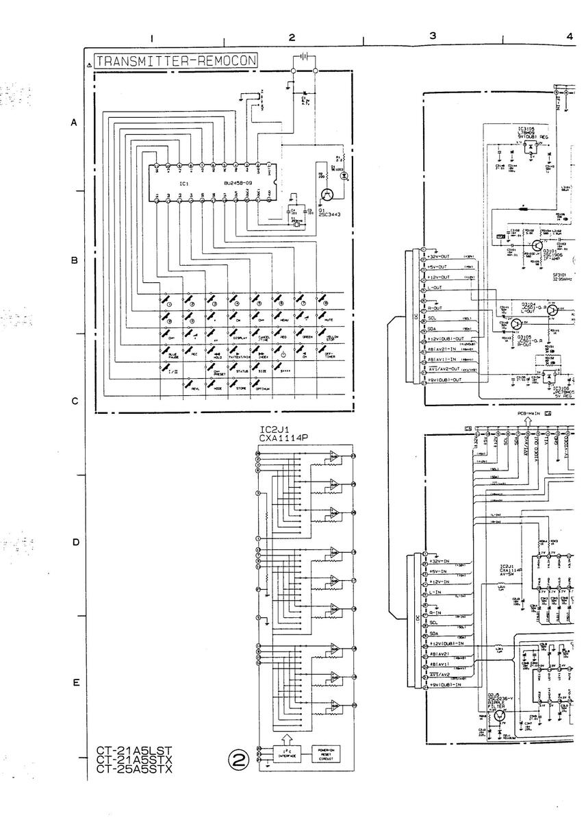
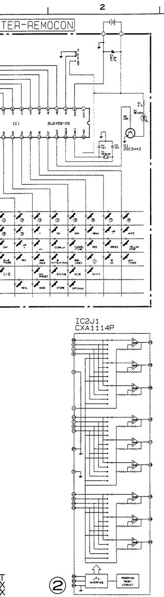
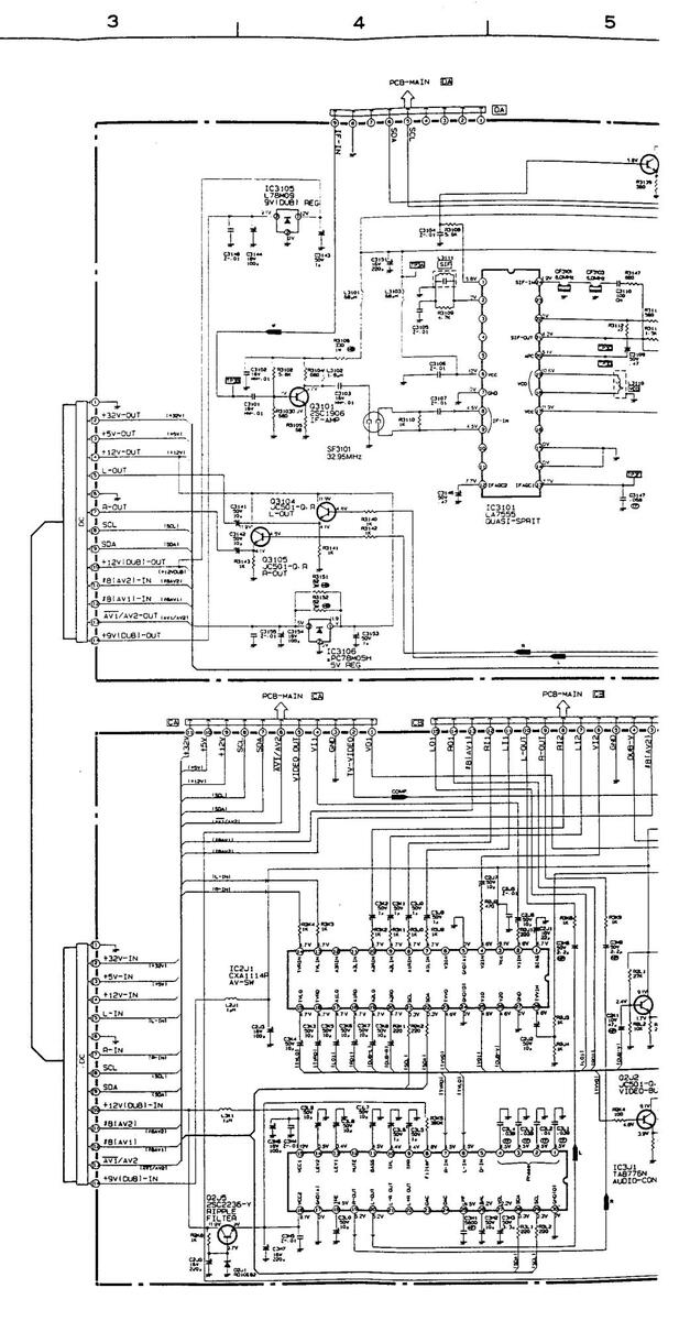
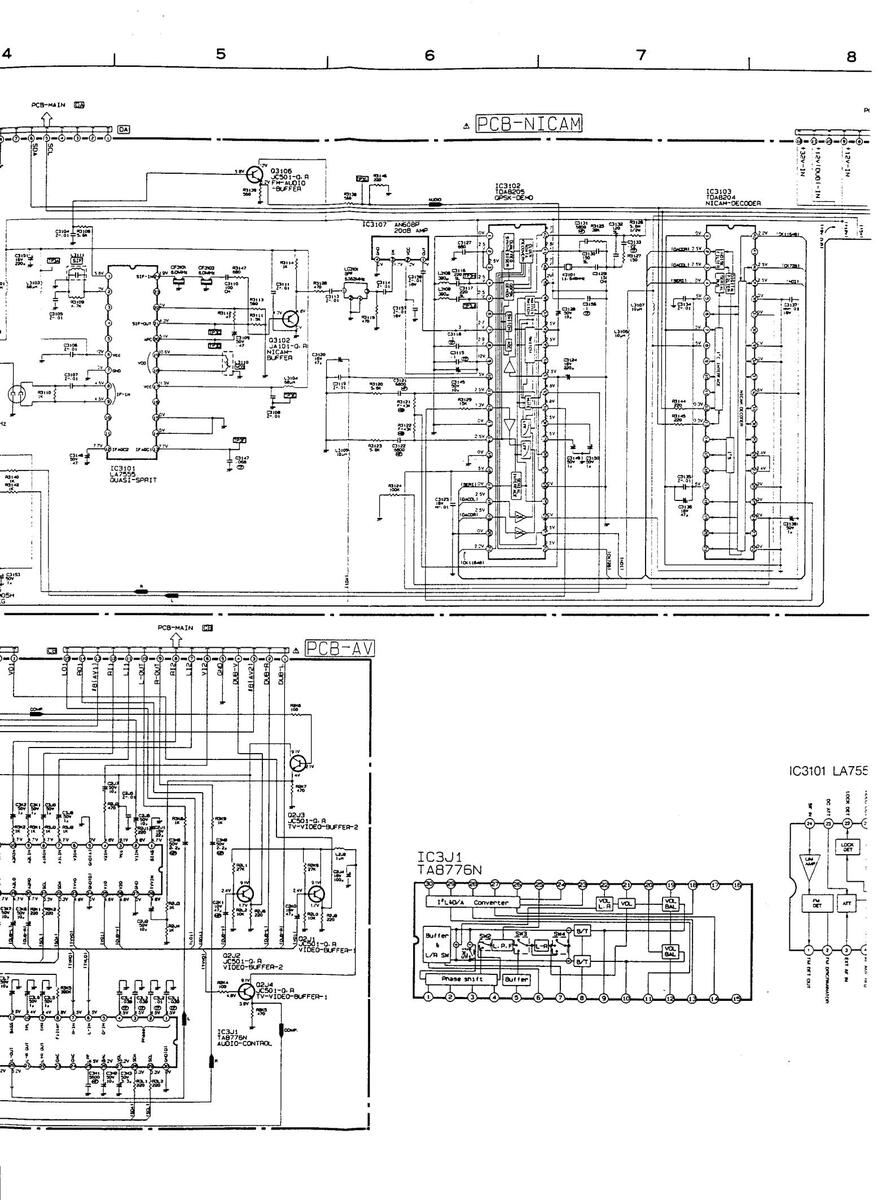
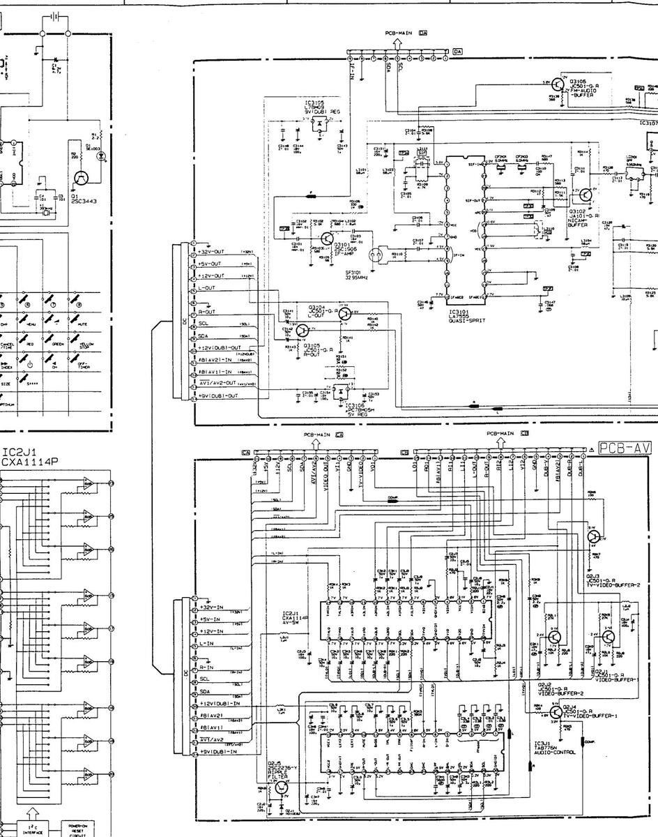
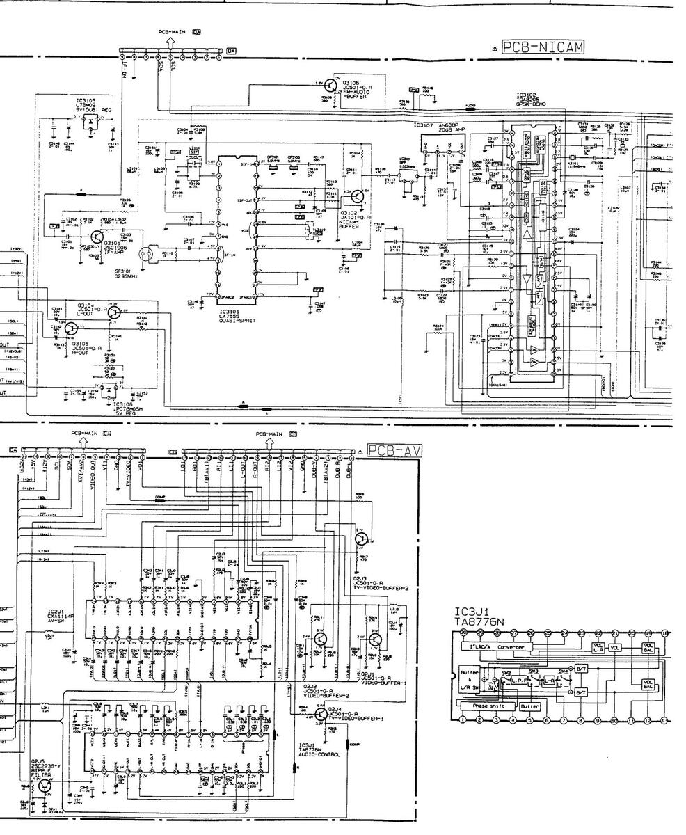
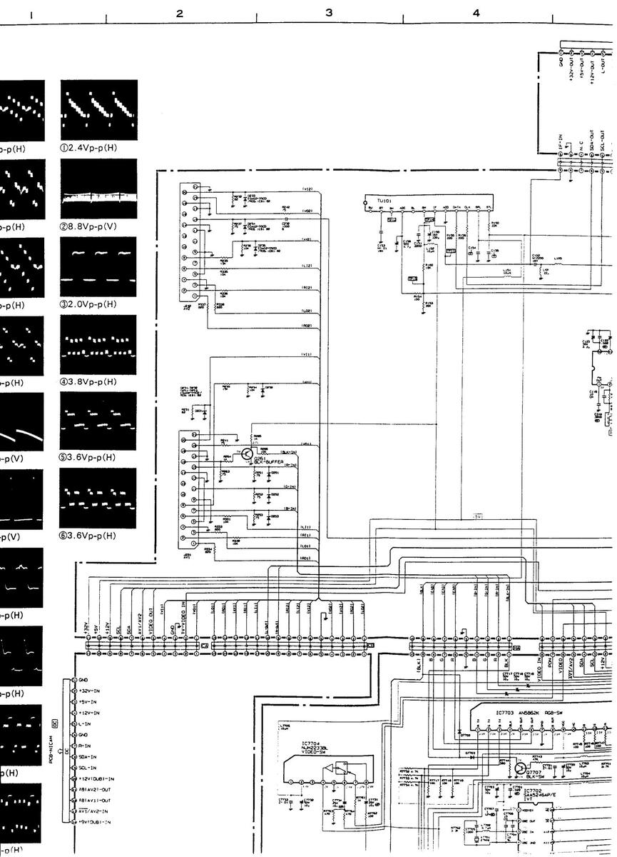
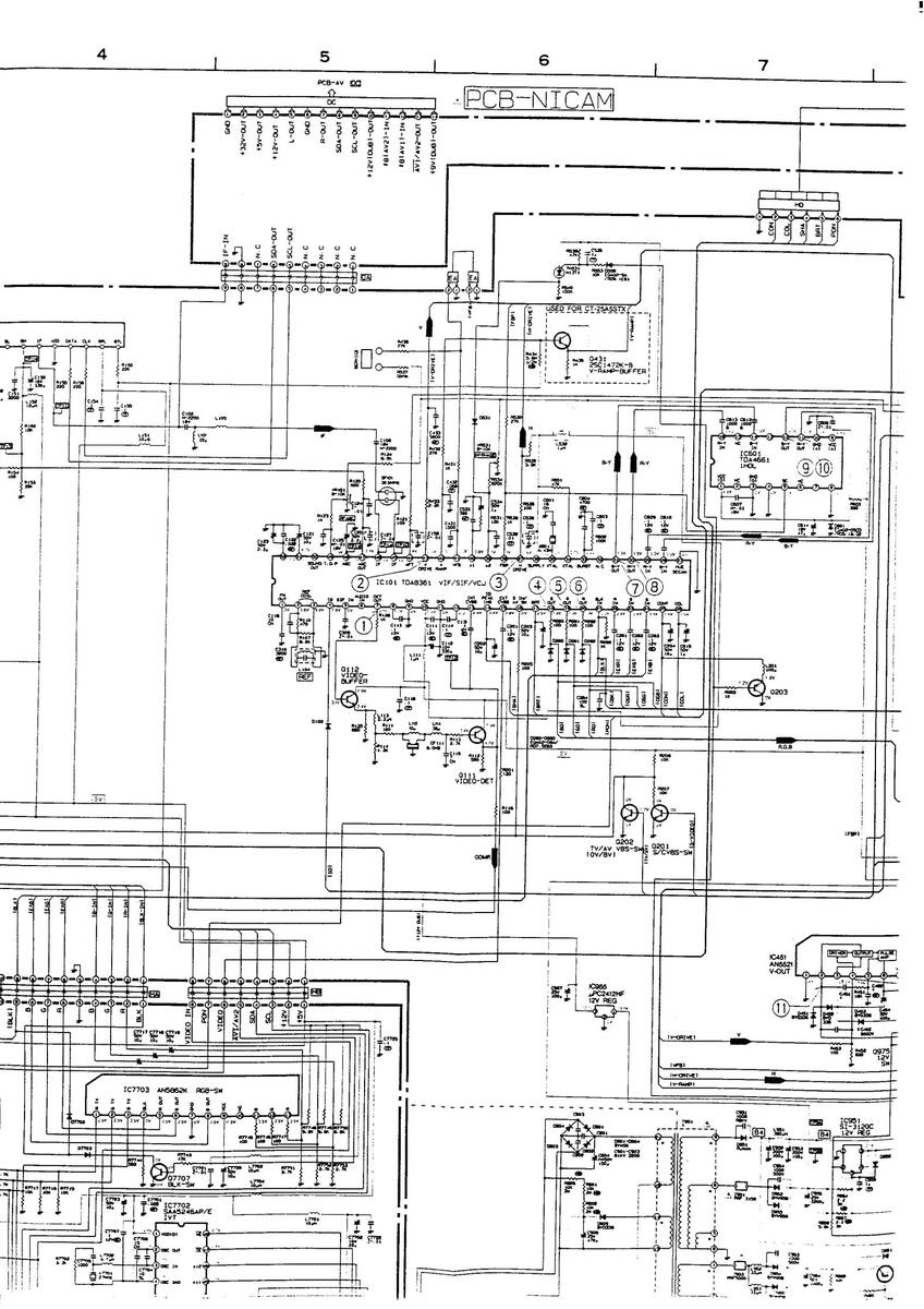
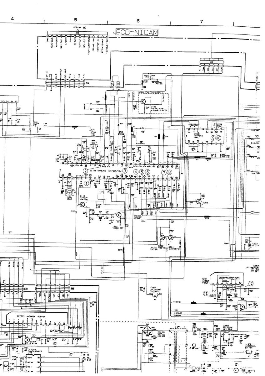
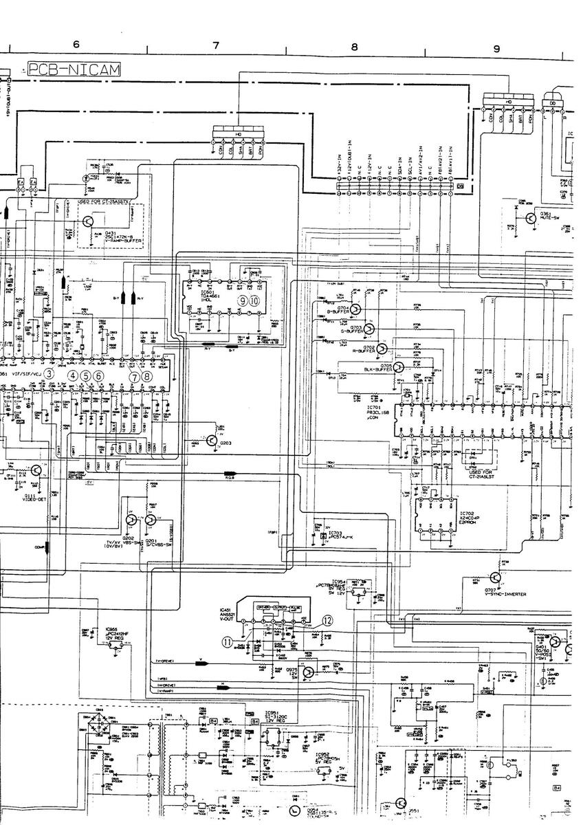
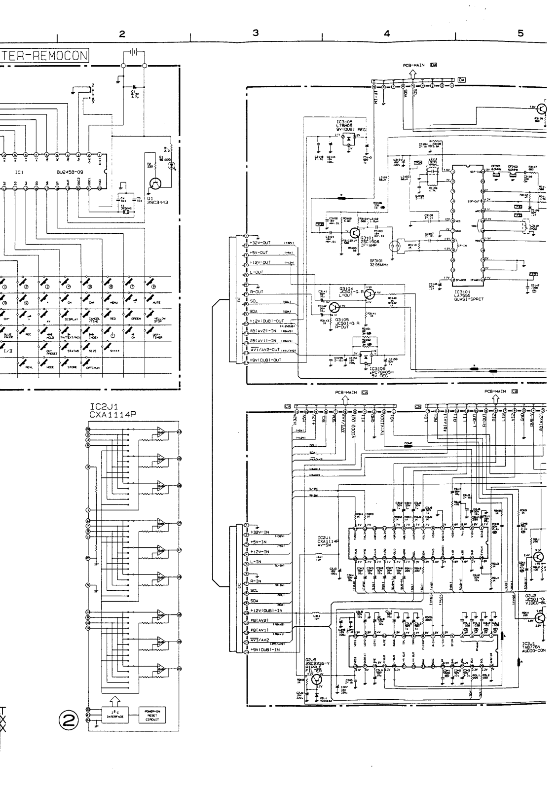
SCHEMA
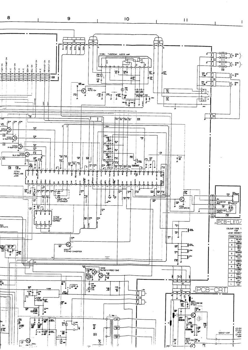
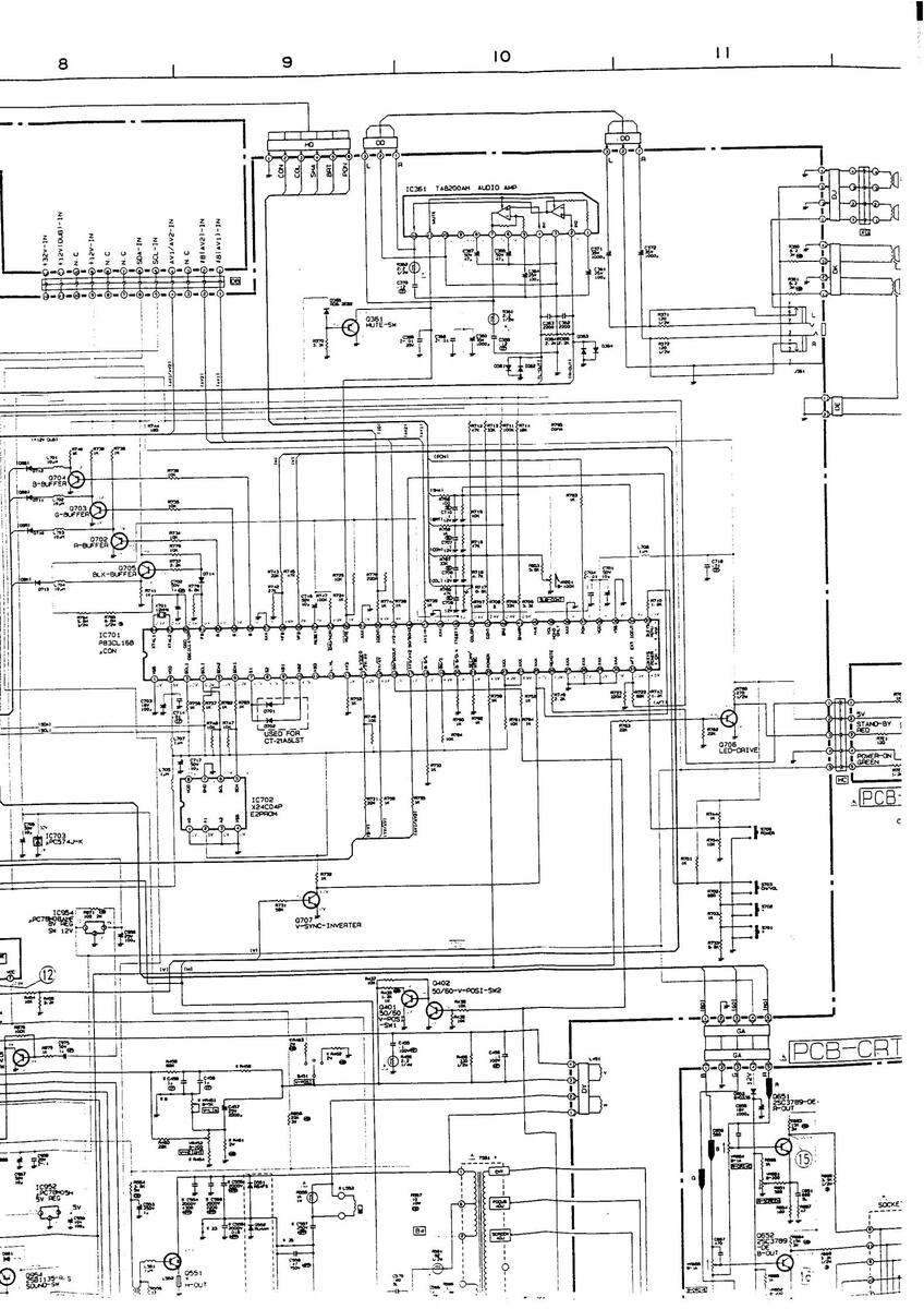
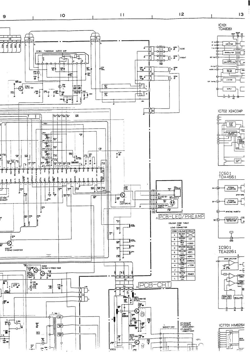
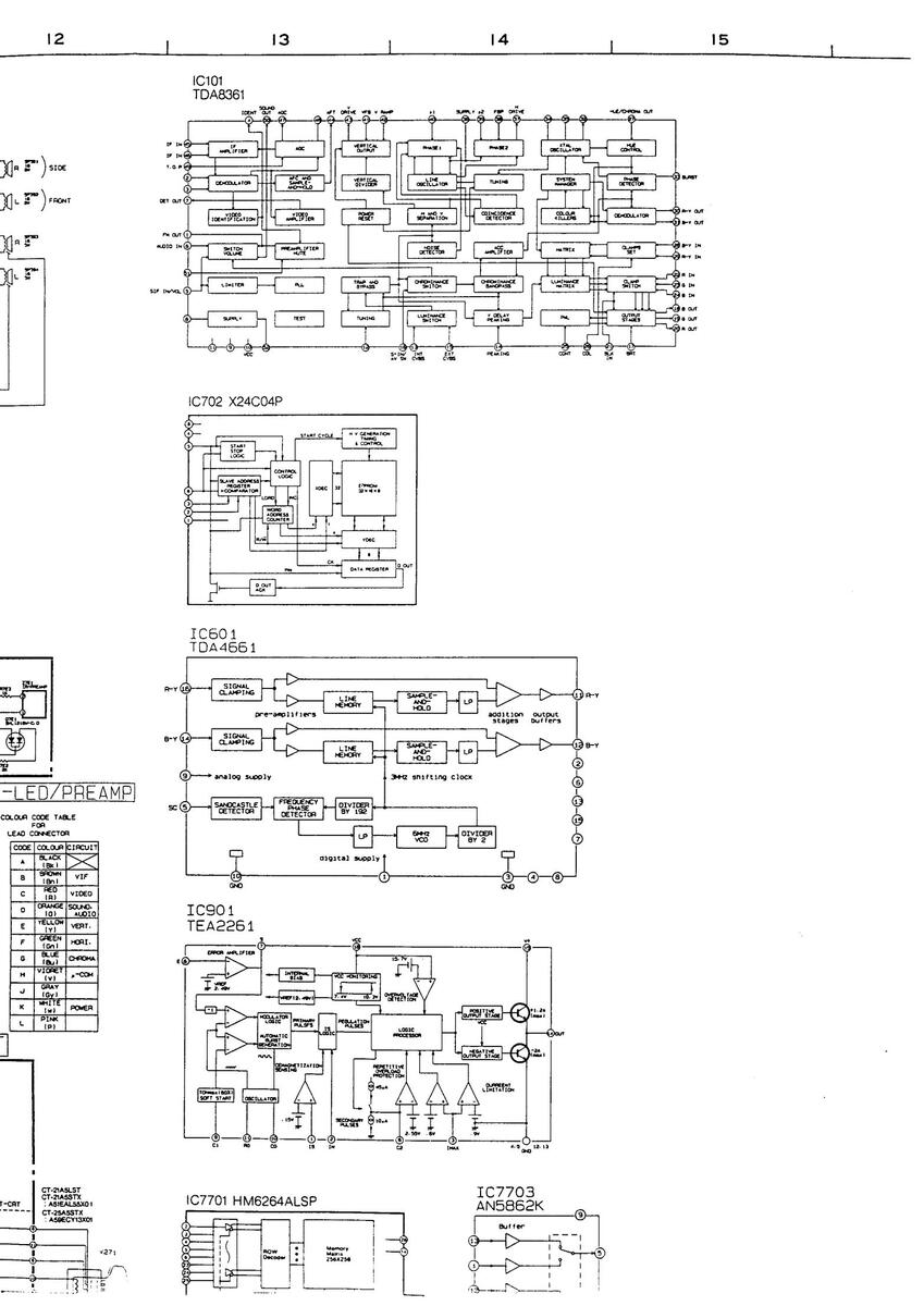
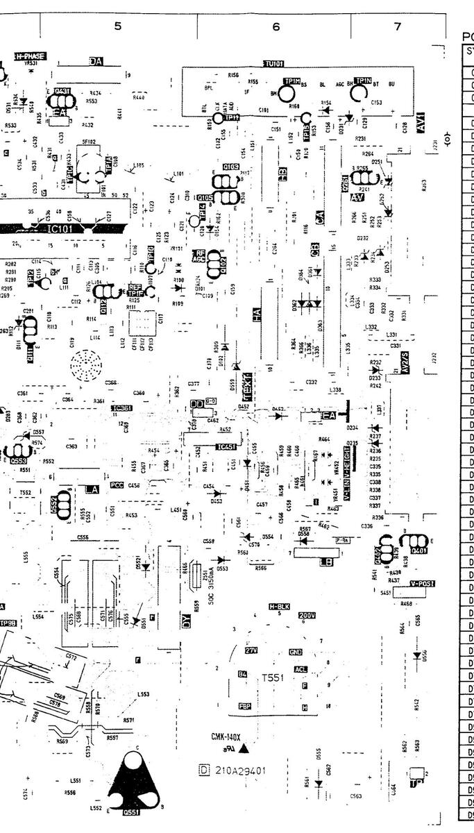
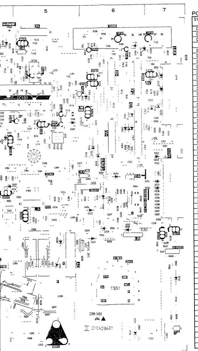
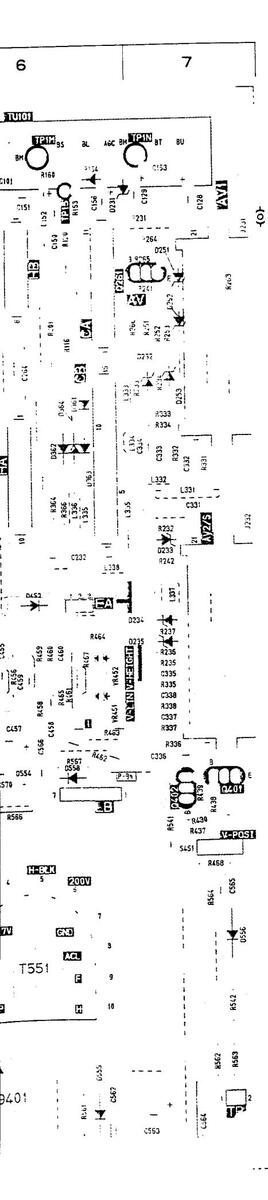
SCHEMATIC DIAGRAM MOE
SCHEMATIC DIAGRAM MODE

SERVICING PRECAUTION
SYMBOLS INDICATE COMPONENTS HAVING SPECIAL CHARACTERISTICS IMPORTANT TO SAFETY AND PERFORMANCE THERFORE REPLACEMENT OF ANY SAFETY PARTS SHOULD BE IDENTICAL IN VALUE AND CHARACTERISTICS . FOR ACCURACY OF THE REPLACEMENT REFER TO THE PARTS LIST OF SERVICE MANUA
DON'T DEGRADE THE SAFETY OF THE RECEIVERS THROUGH IMPROPER SERVICING.
• NOTE
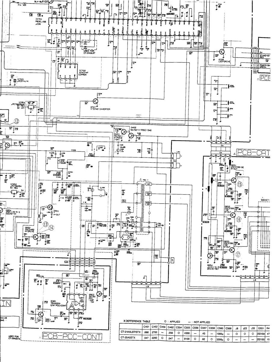
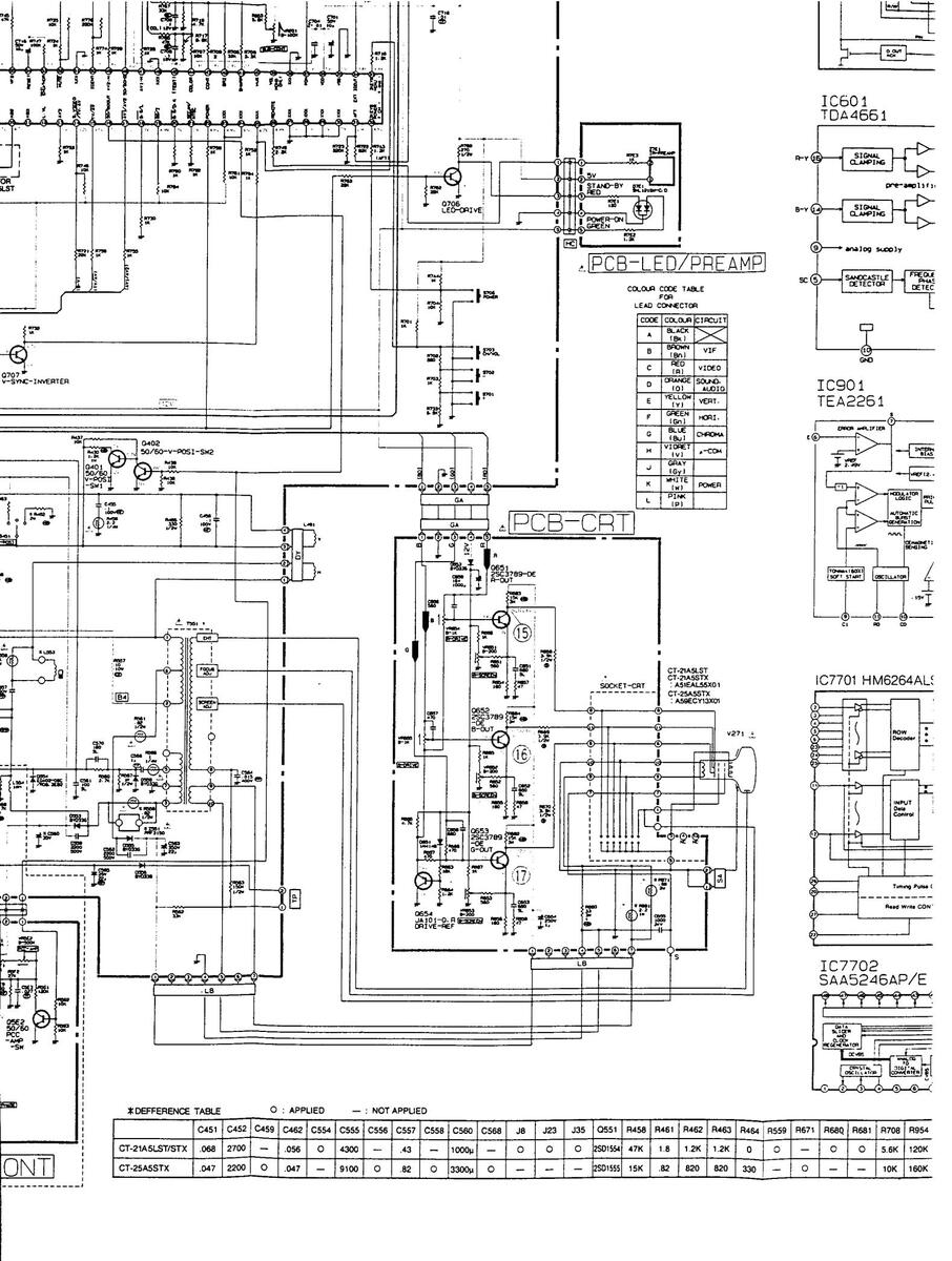
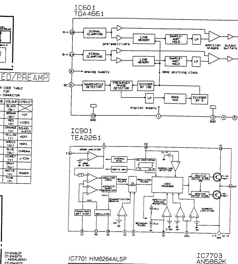
- DC voltages were measured from points indicated to th ground with a high-Z voltmeter. Waveforms were taken with standard colour bar signal. TP6A, etc. show Test Points.
This is a basic schematic diagram. Some sets may be s modification according to engineering improvement.
![]()

Δ
✓
h, it.
T
CT-21A5LST CT-21A5STX A51EAL55 CT-25A5ST)
ſĻ
Э
| 1 | R458 | R461 | R462 | R463 | R464 | R559 | R671 | R680 | R681 | R708 | R954 | R955 | R962 | VB451 | VR951 | 7551 |
|---|---|---|---|---|---|---|---|---|---|---|---|---|---|---|---|---|
| 4 | 47K | 1.8 | 1.2K | 1.2K | 0 | ο | - | 0 | 0 | 5.6K | 120K | 7.5K | - | _ | B10K | _ |
| 5 | 15K | .82 | 820 | 820 | 330 | - | 0 | - | - | 10K | 160K | 8.2K | 0 | ο | B20K | 0 |
CT-21A5LST CT-21A5STX CT-25A5STX

PCB-NICAM
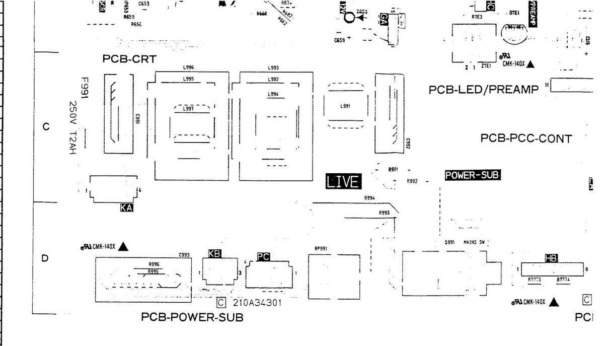
PCB-NICAM
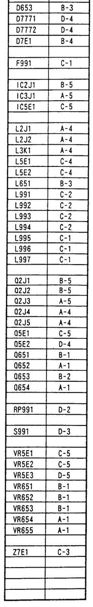
| L996 | C-1 |
| L997 | C-1 |
| 02J1 | 8-5 |
| 02 J 2 | B-5 |
| 02J3 | A-5 |
| 02J4 | A-4 |
| 02J5 | A-4 |
| Q5E1 | C-5 |
| 05E2 | D-4 |
| 0651 | B-1 |
| 0652 | A-1 |
| 0653 | B-2 |
| 0654 | A-1 |
| RP991 | D-2 |
| S991 | D-3 |
| VR5E1 | C-5 |
| VR5E2 | C-5 |
| VR5E3 | D-5 |
| VR651 | 8-1 |
| VR652 | B-1 |
| VR653 | B-1 |
| VR654 | A-1 |
| VR655 | A-1 |
| Z7E1 | C-3 |
| 0011 | 0/11/1 |
|---|---|
|
SYMBOL
NO. |
ADDRESS |
| CF3101 | B-2 |
| CF3103 | B-2 |
| 103101 | B-2 |
| 103102 | B-3 |
| 1C3103 | B-4 |
| IC3105 | B-2 |
| 103106 | A-2 |
| 103107 | B-3 |
| L3101 | A-2 |
| L3101 | B-2 |
| L3102 | 8-2 |
| L3103 | B-2 |
| L3104 | A-2 |
| L3106 | A-3 |
| L3107 | B-4 |
| L3108 | B-3 |
| L3109 | B-3 |
| L3110 | A-2 |
| L3111 | B-2 |
| L3112 | B-3 |
| LC3101 | B-3 |
| 03101 | B-2 |
| 03102 | A-3 |
| 03104 | A-1 |
| 03105 | A-1 |
| 03106 | B-3 |
| SF3101 | B-2 |
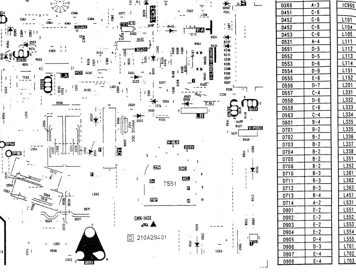
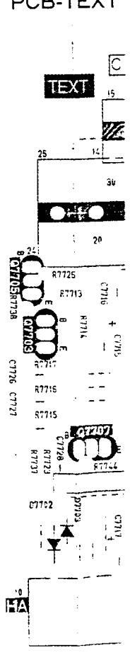
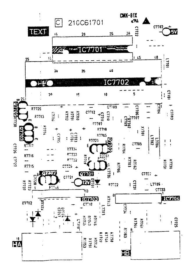
PCB-TEXT
L333 L334
| D365 | A-3 | |
|---|---|---|
| D451 | C-6 | |
| D452 | C-6 | |
| D452 | C-6 | |
| D453 | C-6 | |
| D531 | A-4 | |
| D551 | D-5 | I L |
| D552 | D-5 | |
| D553 | D-6 | |
| D554 | D-6 | ╽╽ |
| D555 | E-6 | ╽╽ |
| D556 | D-7 | ╽┟ |
| D557 | C-4 | |
| D558 | D-6 | |
| D559 | C-6 | ╽╽ |
| D563 | C-4 | ╏┠ |
| D601 | B-4 | |
| D701 | B-2 | |
| D702 | B-2 | |
| D703 | B-2 | |
| D704 | B-2 | |
| D705 | B-2 | |
| D706 | B-2 | |
| D710 | B-3 | |
| D711 | B-3 | |
| D712 | B-3 | |
| D713 | B-4 | |
| D714 | A-2 | |
| D901 | E-2 | |
| D902 | E-2 | |
| D903 | E-2 | |
| D904 | E-2 | |
| D905 | D-4 | |
| D906 | D-3 | |
| D907 | E-4 | |
| 1 0000 | 1 | 1 |
| 1101 4-5 | |
|---|---|
| L104 B-5 | |
| L105 A-5 | |
| L111 B-5 | |
| L112 B-5 | |
| L113 B-5 | |
| L114 B-5 | |
| L151 A-6 | |
| L152 A-6 | 1 |
| L201 C-4 | |
| L331 B-7 | 1 |
| L332 B-7 | |
| L333 B-6 | |
| L334 B-6 | |
| L335 B-6 | |
| L335 B-6 | |
| L336 B-6 | |
| L337 C-7 | |
| L338 C-6 | |
| L351 C-1 | |
| L352 C-1 | |
| L361 B-1 | |
| L362 B-1 | |
| L363 B-1 | |
| L451 C-5 | |
| L531 A-4 | |
| L551 E-5 | |
| L552 E-5 | |
| L553 E-5 | |
| L554 D-5 | |
| L555 D-4 | |
| L701 B-3 | |
| L702 B-3 | |
| L703 B-3 |
| 261 | A-6 | L | |
|---|---|---|---|
| 361 | ٨-3 | E | |
| 401 | D-7 | ||
| 402 | D-7 | ||
| 431 | A-5 | L | |
| 551 | E-5 |
L |
|
| 552 | C-5 | ||
| 553 | C-4 | ||
| 702 | A-3 | - [ |
L |
| 703 | A-3 | ||
| 704 | A-3 | ||
| 705 | A-3 |
L |
|
| 706 | E-1 |
L |
|
| 707 | B-2 | ||
| 901 | E-3 |
L |
|
| 902 | E-4 | ||
| 1953 | D-4 |
L |
|
| 1954 | 8-1 | ||
| 1955 | B-2 | ||
| Γ | |||
| 5451 | D-7 | ||
| 5701 | D-1 | ||
| 5702 | D-1 | L | |
| 5703 | D-1 | ||
| S706 | D-1 | ||
| T | |||
| SF101 | A-5 | ||
| SF102 | A-5 | ||
| Τ | |||
| T551 | E-6 | ||
| T552 | C-4 | ||
| T901 | D-3 | ||
| ] | |||
| TH531 | A-4 | ||
| TU101 | A-6 |
PCB-TEXT
| C-2 | 0261 | A-6 | IL | ||||
|---|---|---|---|---|---|---|---|
| t | 0361 | A-3 | · | ||||
| t | A-5 | 0401 | D-7 | ||||
| t | B-5 | 0402 | D-7 | ||||
| T | ٨-5 | 0431 | A-5 | ||||
| t | B-5 | Q551 | E-5 | ||||
| t | B-5 | 0552 | C-5 | L | |||
| t | B-5 | 0553 | C-4 | ||||
| t | B-5 | 0702 | A-3 | ||||
| t | A-6 | 0703 | A-3 | ||||
| t | A-6 | 0704 | A-3 | L | |||
| t | C-4 | 1 | 0705 | A-3 | • | ||
| t | B-7 | 1 | 0706 | E-1 | 1 | | ||
| t | 8-7 | 1 | 0707 | B-2 | 1 | ||
| t | B-6 | 1 | 0901 | E-3 | 1 | ||
| t | 8-6 | 1 | 0902 | E-4 | 1 | ||
| t | B-6 | 1 | 0953 | D-4 | 1 | ||
| t | B-6 | 1 | 0954 | B-1 | 1 | ||
| 1 | 8-6 | 1 | 0955 | B-2 | 1 | ||
| ┥ | C-7 | 1 | 1 | ||||
| t | 6-6 | 1 | S451 | D-7 | 1 | ||
| ┨ | 1 | S701 | D-1 | ||||
| 1 | C-1 | 1 | $702 | D-1 | 1 | ||
| 1 | S703 | D-1 | 1 | ||||
| 8-1 | 1 | S706 | D-1 | 1 | |||
| B-1 | 1 | 1 | |||||
| C-5 | 1 | SF101 | A-5 | 1 | |||
| A-4 | 1 | SF102 | A-5 | 1 | |||
| F-5 | 1 | 1 | |||||
| F-5 | 1 | T551 | E-6 | 1 | |||
| - | F-5 | 1 | T552 | C-4 | 1 | ||
| D-5 | 1 | T901 | D-3 | 1 | |||
| - | D-4 | 1 | 1 | ||||
| - | B-3 | 1 | TH531 | A-4 | 1 | ||
| 8-3 | 1 | 1 | |||||
| 0.0 | TU101 | A-6 | 1 |
кт

| і B-6 | 1 | 1 10954 | L C-2 | |
|---|---|---|---|---|
| - | A-3 | 1 | 10955 | C-2 |
| C-6 | 1 | |||
| C-6 | 1 | L101 | A-5 | |
| C-6 | 1 | L104 | 8-5 | |
| C-6 | 1 | L105 | A-5 | |
| A-4 | 1 | L111 | B-5 | |
| D-5 | 1 | L112 | 8-5 | |
| D-5 | 1 | L113 | B-5 | |
| D-6 | L114 | B-5 | ||
| D-6 | 1 | L151 | A-6 | |
| E-6 | L152 | A-6 | ||
| D-7 | L201 | C-4 | ||
| C-4 | L331 | B-7 | ||
| D-6 | ] | L332 | B-7 | |
| C-6 | L333 | B-6 | ||
| C-4 | L334 | 8-6 | ||
| B-4 | ] | L335 | 8-6 | |
| B-2 | L335 | 8-6 | ||
| B-2 | ] | L336 | B-6 | |
| B-2 | ] | L337 | C-7 | |
| _ | B-2 | ] | L338 | C-6 |
| 8-2 | L351 | C-1 | ||
| B-2 | L352 | C-1 | ||
| B-3 | L361 | B-1 | ||
| B-3 | L362 | B-1 | ||
| B-3 | L363 | B-1 | ||
| B-4 | L451 | C-5 | ||
| A-2 | L531 | A-4 | ||
| E-2 | L551 | E-5 | ||
| E-2 | L552 | E-5 | ||
| E-2 | L553 | E-5 | ||
| E-2 | L554 | D-5 | ||
| D-4 | L555 | D-4 | ||
| D-3 | L701 | B-3 | ||
| E-4 | L702 | B-3 |
PCB-TEXT
|
YMBOL
NO. |
ADDRESS |
SYMBOL
NO. |
ADDF |
|---|---|---|---|
| F111 | 8-5 | D909 | E-2 |
| F112 | 8-5 | D951 | C-3 |
| F113 | 8-5 | D952 | C-3 |
| D953 | C-3 | ||
| 0101 | B-6 | D954 | D-2 |
| 0102 | 8-6 | D955 | C-4 |
| 0111 | B-4 | D955 | C-4 |
| 154 | 8-6 | D956 | C-2 |
| 231 | A-6 | D958 | D-4 |
| 232 | B-7 | D960 | C-2 |
| 233 | C-7 | D961 | 8-2 |
| 234 | C-7 | 1 | |
| 235 | C-7 | IC101 | 8-5 |
| 251 | A-7 | IC361 | C-5 |
| 252 | A-7 | 10451 | C-F |
| 253 | B-7 | 10601 | B-4 |
| 254 | C-1 | 10631 | A-4 |
| 280 | C-4 | 10001 | A-7 |
| 281 | C-4 | 10702 | 8-0 |
| 201 | 0-4 | 10702 | 0-2 |
| 202 | C-4 | 10703 | |
| 203 | 0-6 | 10901 | |
| 201 | 8-0 | 10951 | |
| 302 | 8-0 | 10952 | 0-2 |
| 304 | 8-0 | 10954 | C-2 |
| 305 | A-3 | 10322 | |
| 451 | |||
| 452 | C-6 | A-5 | |
| 452 | C-6 | L104 | 8-5 |
| 453 | C-6 | L105 | A-5 |
| 531 | A-4 | 8-5 | |
| 551 | 0-5 | 8-5 | |
| 552 | D-5 | B-5 | |
| 553 | 0-6 | B-5 | |
| 554 | 0-6 | L151 | A-6 |
| 555 | E-6 | L152 | A-6 |
| 555 | D-7 | L201 | C-4 |
| 557 | C-4 | L331 | B-1 |
| 558 | 0-6 | L332 | B-1 |
| 559 | C-6 | L333 | 8-6 |
| 563 | C-4 | L334 | 8-6 |
| 601 | B-4 | L335 | B-6 |
| 701 | B-2 | L335 | B-6 |
| 702 | B-2 | L336 | B-6 |
| 703 | B-2 | L337 | C-7 |
| 704 | 8-2 | L338 | C-6 |
| 705 | B-2 | L351 | C-1 |
| 706 | 8-2 | L352 | C-1 |
| 710 | B-3 | L361 | B-1 |
| 711 | B-3 | L362 | B-1 |
| 712 | B-3 | L363 | B-1 |
| 713 | B-4 | L451 | C-5 |
| 714 | A-2 | L531 | A-4 |
| 901 | E-2 | L551 | E-5 |
| 902 | E-2 | L552 | E-5 |
| 903 | E-2 | L'553 | E-5 |
| 904 | E-2 | 1554 | D-5 |
| 905 | D-4 | 1555 | D-4 |
| 906 | D-3 | 1701 | 8-3 |
| 907 | F-4 | 1702 | 8-3 |
| 1702 | 0.3 |
| B-MA | |||
|---|---|---|---|
|
MBOL
NO. |
ADDRESS |
SYMBOL
NO. |
ADDRES |
| F111 | 8-5 | D909 | E-2 |
| F112 | B-5 | D951 | C-3 |
| F113 | 8-5 | D952 | C-3 |
| D953 | C-3 | ||
| 101 | 8-6 | D954 | D-2 |
| 102 | B-6 | D955 | C-4 |
| 111 | 8-4 | D955 | C-4 |
| 154 | 8-6 | 0956 | |
| 0.001 | 1-6 | 0958 | D-4 |
| 231 |
|
D960 | C-2 |
| 232 | D900 | ||
| 233 | 0301 | 0-2 | |
| 234 | 10101 | 0 5 | |
| 235 | D-3 | ||
| 0251 | A-1 | 10301 | |
| 0252 | A-1 | 10451 | 6-6 |
| 0253 | 8-1 | 10001 | 8-4 |
| 0254 | 10031 | A-4 | |
| 0280 | C-4 | A-2 | |
| 0281 | C-4 | 10702 | 8-2 |
| 0282 | C-4 | 10703 | C-3 |
| 0283 | C-4 | 10901 | E-3 |
| 0361 | B-6 | 10951 | C-2 |
| 0362 | 8-6 | 10952 | C-2 |
| 0364 | B-6 | 1C954 | C-2 |
| 0365 | A-3 | 10955 | C-2 |
| 0451 | C-6 | ||
| 0452 | C-6 | L101 | A-5 |
| 0452 | C-6 | L104 | B-5 |
| 0453 | C-6 | L105 | A-5 |
| 0531 | A-4 | L111 | B-5 |
| 0551 | D-5 | L112 | B-5 |
| 0552 | D-5 | L113 | 8-5 |
| D553 | D-6 | L114 | B-5 |
| D554 | D-6 | L151 | A-6 |
| D555 | E-6 | L152 | A-6 |
| D556 | D-7 | L201 | C-4 |
| D557 | C-4 | L331 | 8-7 |
| D558 | D-6 | L332 | B-7 |
| D559 | C-6 | L333 | B-6 |
| D563 | C-4 | L334 | B-6 |
| D601 | 8-4 | L335 | 8-6 |
| D701 | B-2 | L335 | B-6_ |
| D702 | B-2 | L336 | 8-6 |
| D703 | B-2 | L337 | C-7 |
| D704 | B-2 | L338 | C-6 |
| D705 | B-2 | L351 | C-1 |
| D706 | B-2 | L352 | C-1 |
| D710 | 8-3 | L361 | B-1 |
| D711 | B-3 | L362 | B-1 |
| D712 | B-3 | L363 | 8-1 |
| D713 | B-4 | L451 | C-5 |
| D714 | A-2 | L531 | A-4 |
| D901 | E-2 | L551 | E-5 |
| D902 | E-7 | L552 | E-5 |
| 0002 | F-7 | 1 1553 | E-5 |
| D004 | F-7 | D-5 | |
| D904 | D-4 | 1 555 | D-4 |
| 0303 | D-3 | 1 701 | 8-3 |
| 0007 | F-4 | 1 1702 | B-3 |
| 0301 | E-4 | B-3 | |
| 0900 |
| B-INIA | _ | ||||
|---|---|---|---|---|---|
|
MBOL
NO. |
ADDRESS |
SYMBOL
NO. |
A | DDRESS | |
| F111 | 8-5 | D909 | E-2 | ||
| F112 | B-5 | D951 | C-3 | ||
| F113 | B-5 | | [ | D952 | C-3 | |
| D953 | C-3 | ||||
| 101 | 8-6 | D954 | D-2 | ||
| 102 | B-6 | D955 | C-4 | ||
| 111 | B-4 | D955 | C-4 | ||
| 154 | B-6 | ] [ | D956 | C-2 | |
| 231 | A-6 | D958 | D-4 | ||
| 232 | 8-7 | D960 | C-2 | ||
| 233 | C-7 | D961 | 8-2 | ||
| 0234 | C-7 | ||||
| 0235 | C-7 | 10101 | ╞ | B-5 | |
| 0251 | A-7 | 10361 | 1 | C-5 | |
| 0252 | A-7 | 10451 | C-6 | ||
| 0253 | B-7 | 10601 | 8-4 | ||
| D254 | C-1 | 10631 | A-4 | ||
| D280 | C-4 | 10701 | ╞ | A-2 | |
| D281 | C-4 | 10702 | 1. | 8-2 | |
| D282 | C-4 | 10703 | C-3 | ||
| D283 | C-4 | 10901 | +- | E-3 | |
| D361 | B-6 | 10951 | ╋ | ||
| D362 | B-6 | - | 10952 | ┿ | |
| D364 | 8-6 | ┥ | 10954 | + | |
| D365 | A-3 | - | 10922 | ╋ | |
| D451 | ┥ | 1 101 | ╉ | A-5 | |
| D452 | C-6 | - | 1104 | ╉ | |
| D452 | C-6 | - | 1105 | ┽ | A-5 |
| 0531 | A-4 | 1 | L111 | T | 8-5 |
| D551 | D-5 | 1 | L112 | B-5 | |
| D552 | D-5 | L113 | B-5 | ||
| D553 | D-6 | L114 | 8-5 | ||
| D554 | D-6 | L151 | A-6 | ||
| D555 | E-6 | L152 | _ | A-6 | |
| D556 | D-7 | L201 | _ | C-4 | |
| D557 | L331 | _ | 8-7 | ||
| D558 | D-6 | L332 | ╉ | B-7 | |
| D559 | L333 | -+ | B-6 | ||
| D563 | - | L334 | -+ | 8-6 | |
| D601 | 8-4 | 4 | L335 | -+ | |
| D701 | 8-2 | - | L335 | -+ |
|
| D702 | B-2 | - | 1227 | -+ | |
| 0703 | D-2 | - | 1339 | + | |
| D705 | B-2 | 1 351 | -† | C-1 | |
| D705 | B-2 | - | 1352 | ╡ | C-1 |
| D710 | 8-3 | L361 | - | 8-1 | |
| D711 | B-3 | L362 | 8-1 | ||
| D712 | B-3 | L363 | B-1 | ||
| D713 | 8-4 | L451 | C-5 | ||
| D714 | A-2 | L531 | A-4 | ||
| D901 | E-2 | L551 | E-5 | ||
| D902 | E-2 | L552 | E-5 | ||
| D903 | E-2 | L553 | E-5 | ||
| D904 | E-2 | L554 | D-5 | ||
| D905 | D-4 | L555 | D-4 | ||
| D906 | D-3 | L701 | B-3 | ||
| D907 | E-4 | L702 | 8-3 | ||
| 008 | F-4 | 1 1703 | 1 8-3 |
PC SY
| [ | YMBOL | A | DDRESS | ſ | |
| NO. | |||||
| L704 | L | 8-3 | |||
| L705 | B-2 | ||||
| L706 | L | A-1 | |||
| L707 | 8-3 | ||||
| 1 | Γ | L901 | E-4 | ||
| 1 | Γ | L902 | Γ | E-4 | |
| L903 | E-3 | ||||
| 1 | 1904 | Γ | E-3 | ||
| ┢ | 1 905 | ┢ | E-3 | ||
| ┢ | 1.051 | ┢ | C-4 | ||
| ┢ | 1053 | ┼╴ | |||
| ┝ | L952 | ╀ | ł | ||
| ⊢ | L953 | ┿ | 6-2 | ||
| Ļ | ╀ | ł | |||
| PC951 | ╀ | U-4 | ł | ||
| L | ╞ | ||||
| 0102 | 8-6 | ||||
| ſ | 0103 | A-6 | ļ | ||
| 1 | Γ | 0105 | A-6 | 1 | |
| 1 | ſ | 0106 | Τ | 8-3 | |
| 1 | T | Q111 | T | B-4 | |
| 1 | t | 0112 | Τ | B-5 | 1 |
| ł | 0201 | t | B-2 | 1 | |
| ┨ | ł | 0202 | ╉ | B-2 | 1 |
| - | ┠ | 0202 | + | 1 | |
| - | ł | 0203 | ╉ | ||
| 4 | ┟ | u261 | ╋ | ┨ | |
| 4 | 0361 | ╋ | A-3 | ||
| 0401 | ╞ | ||||
| 0402 | - | D-1 | |||
| 0431 | _ | A-5 | 4 | ||
| 0551 | E-5 | ||||
| 0552 | C-5 | ||||
| ٦ | 0553 | C-4 | |||
| ſ | 0702 | A-3 | |||
| 0703 | Т | A-3 | |||
| 0704 | 1 | A-3 | |||
| 0705 | A-3 | ||||
| -1 | 0706 | E-1 | ٦ | ||
| - | 0707 | 1 | 8-2 | 1 | |
| -1 | 0001 | + | F-3 | ||
| - | 0002 | ┥ |
F-4 |
1 | |
| ┥ | 0052 | ┥ | - | ||
| - | 0054 | + |
1 |
- | |
| 0055 | - | ┥ | |||
| 0922 | 0-2 | - | |||
| _ | - | ||||
| $451 | D-7 | - | |||
| S701 | 0-1 | ||||
| S702 | D-1 | ||||
| S703 | D-1 | ||||
| S706 | D-1 | ||||
| SF101 | A-5 | ||||
| SF102 | A-5 | ||||
| 1 | ٦ | ||||
| - | 1 | T551 | F-6 | ||
| 1 | TEE? | C-4 | 4 | ||
| T001 | |||||
| 1-1901 | U-3 | - | |||
| | | - | ||||
| TH531 | A-4 | ||||
| | | |||||
| TU101 | A-6 | ||||
| SYMBOL | ADDDESS | |
| NO. | | AUUNESS | |
| VK101 | 8-5 | |
| VR201 | A-3 | |
| VR451 | 6-0 | |
| 10451 | ||
| VR452 | C-6 | |
| VR531 | A-4 | |
| VR951 | D-4 | |
| 11331 | ||
| X601 | A-4 | |
| ¥701 | A-3 | |
| || | ||
| Z551 | D-6 | |
| 7951 | C-3 | |
| 7052 | ||
| 2953 | U-3 | |
| 1 | ||
| 4 | ||
| ĺ | ||
| 1 | ||
| ļ | + | |
| 1 | ||
| ┣━━━━━ | + | ł |
| 1 | ||
| 1 | ||
| J | ł | |
| l | ||
| ł | ||
| 1 | ||
| ł | ||
| ł | ||
| L | ||
| 1 | ||
| 1 | ||
| L | ┨ | |
| ł | ||
| 1 | ||
| ┥ | ||
| 1 | ||
| - | ||
| L | ||
| 1 | ||
| 1 | ||
| 4 | ||
| - | ||
| - | ||
| L | ||
| | | + | |
| _ | ||
| 1 | _ | |
| | | ||
| L | ||
| - | ||
PCB-TEXT
| s | NO. | ADDRESS | ||
|---|---|---|---|---|
| - | 1704 | B-3 | ||
| - | 1705 | B-2 | ||
| 1706 | A-1 | |||
| _ | D-3 | |||
| _ | L901 | E-4 | ||
| L902 | E-4 | |||
| L903 | E-3 | |||
| L904 | E-3 | |||
| L905 | E-3 | |||
| L951 | C-4 | |||
| L952 | C-2 | |||
| L953 | C-2 | |||
| - | ||||
| - | PC951 | D-4 | ||
| - | 0102 | 8-6 | ||
| 0103 | 4-6 | |||
| 0105 | 4-6 | |||
| 0105 | A-0 | |||
| 0111 | 0-3 | |||
| D-4 | ||||
| 8-5 | ||||
| 0201 | B-2 | |||
| 0202 | B-2 | |||
| 0203 | C-4 | |||
| 0261 | A-6 | |||
| Q361 | A-3 | |||
| 0401 | D-7 | |||
| 0402 | D-7 | |||
| 0431 | A-5 | |||
| 0551 | E-5 | |||
| Q552 | C-5 | |||
| Q553 | C-4 | |||
| 0702 | A-3 | |||
| 0703 | A-3 | |||
| 0704 | A-3 | |||
| 0705 | A-3 | |||
| - | 0706 | F-1 | ||
| _ | 0707 | D 1 | ||
| _ | 0001 |
D-2
E 2 |
||
| _ | 0901 | E-3 | ||
| 0902 | E-4 | |||
| 0953 | D-4 | |||
| 0954 | B-1 | |||
| 0955 | 8-2 | |||
| S451 | D-7 | |||
| S701 | D-1 | |||
| S702 | D-1 | |||
| S703 | D-1 | |||
| 1 | $706 | D-1 | ||
| 1 | ||||
| 1 | SE101 | 4-5 | ||
| SE102 | ||||
| - | 35102 | A-2 | ||
| _ | 7754 | |||
| _ | 1551 | E-6 | ||
| _ | T552 | C-4 | ||
| T901 | D-3 | |||
| TH531 | A-4 | |||
| TU101 | A-6 | |||
| • |
ES
|
SYMBOL
NO. |
ADDRESS |
|---|---|
| V8101 | B-5 |
| VR201 | A-3 |
| 10201 | |
| VR451 | L-0 |
| VR452 | C-6 |
| VR531 | A-4 |
| VR951 | D-4 |
| VCOI | |
| 1001 | A-4 |
| X701 | A-3 |
| 7551 | 0-6 |
| 7051 | C-3 |
| 2331 | |
| 2953 | D-3 |
| 11 | |
| + | | |
| ∔ ┨ | |
| ļ | |
| 1 | |
| +1 | |
| | | | |
| 11 | |
| ļ | |
| 1 | |
| ∔ | |
| ļł | |
| 1 | |
| ╂┫ | |
| ╂────┨ | |
| | | |
| 1 1 | |
| ┼───┨ | |
| ∔ | |
| | | | |
| |1 | |
| || | |
| + | |
| ∔ł | |
| ┨────┨ | |
| +I | |
| ļl | |
PCB-NICAM
|
SYMBOL
NO. |
ADDRESS | Γ |
SYMBC
NO. |
|
| 1 | L704 | 8-3 | ||
| 1 | L705 | 8-2 | VR101 | |
| 1 | L706 | A-1 | VR201 | |
| 1 | L707 | B-3 | VR451 | |
| 1 | L901 | E-4 | VR452 | |
| 1 | L902 | E-4 | | [ | VR531 |
| 1 | L903 | E-3 | | [ | VR951 |
| 1 | L904 | E-3 | ||
| J | L905 | E-3 | |[ | X601 |
| J | L951 | C-4 | |[ | X701 |
| L952 | C-2 | |||
| 1 | L953 | C-2 | Z551 | |
| Z951 | ||||
| PC951 | D-4 | Z953 | ||
| 0102 | B-6 | |||
| 0103 | A-6 | ļļ | ||
| 0105 | A-6 | |||
| 0106 | B-3 | |||
| 0111 | B-4 | |||
| 0112 | B-5 | |||
| 0201 | B-2 | |||
| 0202 | 8-2 | |||
| ļ | 0203 | C-4 | ||
| 0261 | A-6 | |||
| 0361 | A-3 | ╡╞ | ||
| 0401 | ╡╏ | |||
| - | 0402 | ┥╽ | ||
| 0431 | A-5 | ╡╽ | ||
| 0551 | L-3 | ┥╽ | ||
| 0552 | ||||
| 0702 |
L-4
A-2 |
┥╽ | ||
| - | 0702 | A-3 | ╡╏ | · |
| 0704 | A-3 | |||
| - | 0705 | A-3 | 1 | | |
| 0706 | E-1 | 1 | | ||
| 0707 | B-2 | 1 | | ||
| - | 0901 | E-3 | 11 | |
| 0902 | E-4 | 1 | | ||
| - | 0953 | D-4 | 1 | | |
| 0954 | 8-1 | 1 | ||
| 0955 | B-2 | 1 | ||
| 1 | ||||
| S451 | D-7 | 1 | ||
| S701 | 0-1 | 1 | ||
| $702 | D-1 | |||
| S703 | D-1 | |||
| S706 | D-1 | |||
| _ | ||||
| _ | SF101 | A-5 | ||
| SF102 | A-5 | |||
| _ | ||||
| T551 | E-6 | |||
| T552 | C-4 | L | ||
| T901 | D-3 | |||
| _ | | | - | | 4 | | |
| TH531 | A-4 | |||
| + | 4 | | | ||
| L TU101 | I |
|
'MBOL
NO. |
ADDRESS | |||
|---|---|---|---|---|
| F | ||||
| R101 | 8-5 | |||
| R201 | A-3 | |||
| R451 | C-6 | ſ | ||
| R452 | C-6 | _ | ||
| R531 | A-4 | ä | ||
| R951 | D-4 | × W | ||
| بند . | ||||
| 601 | A-4 | |||
| 701 | A-3 | Δ | - E$_' × | |
| 551 | D-6 | TEA | ||
| 051 | C-3 | |||
| 052 | D-3 | 1665 | ||
| .500 | 03 | |||
| ्रे त क्षु ३६ | ||||
| ļ | ||||
| ļ | > R606 | |||
| ļ | ||||
| ļ | ||||
| в | ||||
| PC | ||||
| 99 | ||||
| 2 | ||||
| 50 | ||||
| С | ||||
| r | ||||
| 1 | ||||
| ۲ ــــــــــــــــــــــــــــــــــــ | ||||
| 1 | ||||
| 1 | 3744 СМК-140) | |||
| 1 | D | - | ||
| 1 | _ | |||
| 1 | ||||
| 1 | 1 | |||
| 1 | 1 | L | ||
| 1 | L | - | ||
| 1 | ||||
| 1 | ||||
| 1 | ||||
| 1 | ||||
| 1 | ||||
| - | ||||
| + | 4 |
PCB-NICAM
PCB-NICAM
2
з
SYMBOL NO. D2J1
DSE1
D651 D652
ADDRESS
8-1
| З | 4 |
| 3 | 4 |
| PCB-NICAM | ||||
|---|---|---|---|---|
|
SYMBOL
NO. |
ADDRESS | |||
| CF3101 | 8-2 | |||
| CF3103 | B-2 | |||


 Loading...