

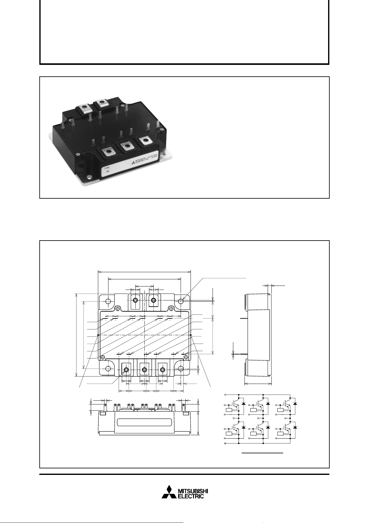
CM50TU-24F
MITSUBISHI IGBT MODULES
CM50TU-24F
HIGH POWER SWITCHING USE
¡IC..................................................................... 50A
CES ......................................................... 1200V
¡V
¡Insulated Type
¡6-elements in a pack
APPLICATION
General purpose inverters & Servo controls, etc
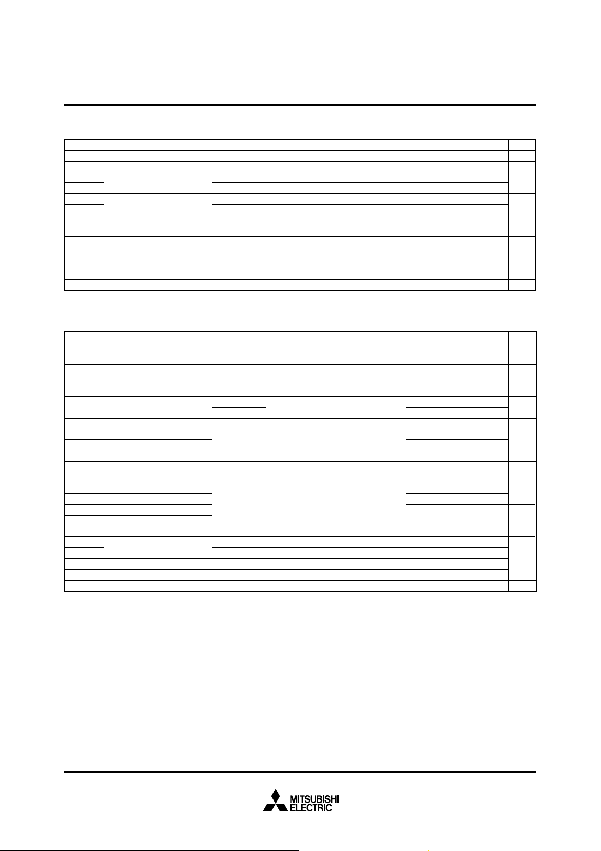
OUTLINE DRAWING & CIRCUIT DIAGRAM
102
±0.25
80
20
10 10
91
±0.25
74
CM
N
11 11 1119.1 19.1 11.85
GuP
GE GE GE
EuP
GvP
EvP
GwP
EwP
5–M4NUTS
GE GE GE
U
10
20
11 19.1
2.8
7.1
V
10 10
P
W
20
11 19.1
3.05
11
4
LABEL
4–φ5.5
MOUNTING HOLES
GuN
EuN
GvN
EvN
GwN
39.3 18.7 1.25
EwN
1.25
Tc measured pointTc measured point
26 8.1
0.5
29
P
G
U
PG
U
PE
E
G
U
NG
E
U
NE
N
V
PG
RTC RTCRTC
V
UV
PE
V
NG
RTC RTCRTC
V
NE
CIRCUIT DIAGRAM
+1
–0.5
Dimensions in mm
(4)
W
P
W
P
W
W
N
W
N
Aug. 1999
MAXIMUM RATINGS (Tj = 25°C)
MITSUBISHI IGBT MODULES
CM50TU-24F
HIGH POWER SWITCHING USE
Symbol Parameter
CES
V
VGES
IC
ICM
IE (
IEM (
PC (
Tj
Tstg
Viso
Collector-emitter voltage
Gate-emitter voltage
Collector current
Note 1
)
Emitter current
Note 1
)
Maximum collector dissipation
Note 3
)
Junction temperature
Storage temperature
Isolation voltage
—
Torque strength
—
Weight
ELECTRICAL CHARACTERISTICS
Symbol
ICES
V
GE(th)
IGES
VCE(sat)
Cies
Coes
Cres
QG
td(on)
tr
td(off)
tf
trr (
Qrr (
VEC(
Rth(j-c)Q
th(j-c)R
R
th(c-f)
R
Rth(j-c’)Q
G
R
Note 1. IE, VEC, trr, Qrr, die/dt represent characteristics of the anti-parallel, emitter to collector free-wheel diode. (FWDi).
1 : Tc measured point is indicated in OUTLINE DRAWING.
*
2 : Typical value is measured by using Shin-etsu Silicone “G-746”.
*
3 : If you use this value, Rth(f-a) should be measured just under the chips.
*
Collector cutoff current
Gate-emitter threshold voltage
Gate leakage current
Collector-emitter saturation voltage
Input capacitance
Output capacitance
Reverse transfer capacitance
Total gate charge
Turn-on delay time
Turn-on rise time
Turn-off delay time
Turn-off fall time
Reverse recovery time
Note 1
)
Reverse recovery charge
Note 1
)
Emitter-collector voltage
Note 1
)
Thermal resistance
Contact thermal resistance
Thermal resistance
External gate resistance
2. Pulse width and repetition rate should be such that the device junction temp. (T
3. Junction temperature (T
4. Pulse width and repetition rate should be such as to cause negligible temperature rise.
Parameter
*1
j) should not increase beyond 150°C.
G-E Short
C-E Short
C = 25°C
T
Pulse (Note 2)
C = 25°C
T
Pulse (Note 2)
C = 25°C
T
Main terminal to base plate, AC 1 min.
Main Terminal M4
Mounting holes M5
Typical value
(Tj = 25°C)
VCE = VCES, VGE = 0V
C = 5.0mA, VCE = 10V
I
V
GE = VCES, VCE = 0V
j = 25°C
T
j = 125°C
T
CE = 10V
V
GE = 0V
V
CC = 600V, IC = 50A, VGE = 15V
V
V
CC = 600V, IC = 50A
GE1 = VGE2 = 15V
V
G = 6.3Ω, Inductive load switching operation
R
E = 50A
I
I
E = 50A, VGE = 0V
IGBT part (1/6 module)
FWDi part (1/6 module)
Case to fin, Thermal compoundapplied
Tc measured point is just under the chips
Conditions UnitRatings
Test conditions
Min. Max.
—
5
—
I
C = 50A, VGE = 15V
—
—
—
—
—
—
—
—
—
—
—
—
—
—
—
*2
(1/6 module)
—
—
6.3
j) does not exceed Tjmax rating.
1200
±20
50
100
50
100
320
–40 ~ +150
–40 ~ +125
2500
1.3 ~ 1.7
2.5 ~ 3.5
570
Limits
T yp.
—
6V
—
1.8
1.9
—
—
—
550
—
—
—
—
—
2.1
—
—
—
0.11
—
—
1
7
20
2.4
—
20
0.85
0.5
—
100
50
300
300
150
—
3.2
0.39
0.70
—
0.31
63
V
V
A
A
W
°C
°C
V
N • m
N • m
g
Unit
mA
µA
V
nF
nC
ns
ns
µC
V
°C/W
✽3
Ω
Aug. 1999
MITSUBISHI IGBT MODULES
CM50TU-24F
HIGH POWER SWITCHING USE
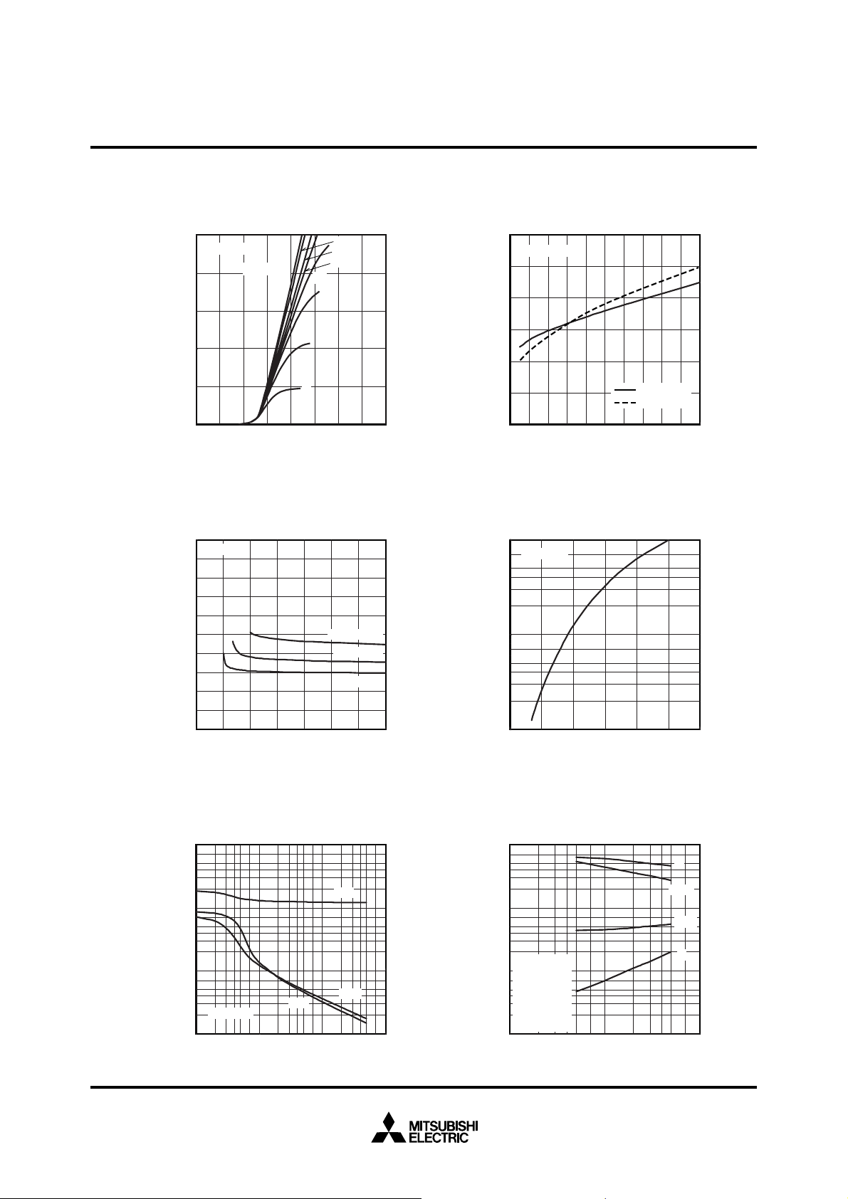
PERFORMANCE CURVES
OUTPUT CHARACTERISTICS
100
Tj=25°C
(A)
C
80
60
40
20
COLLECTOR CURRENT I
0
0 0.5 1 1.5 2 2.5 3 3.5 4
COLLECTOR-EMITTER VOLTAGE V
COLLECTOR-EMITTER SATURATION
VOLTAGE CHARACTERISTICS
5
Tj = 25°C
(V)
4
CE (sat)
3
2
COLLECTOR-EMITTER
1
SATURATION VOLTAGE V
0
6 8 10 12 14 16 18 20
(TYPICAL)
VGE=20V
(TYPICAL)
8
9.5
9
8.5
15
11
10
IC = 100A
IC = 50A
IC = 20A
CE
(V)
COLLECTOR-EMITTER SATURATION
VOLTAGE CHARACTERISTICS
(TYPICAL)
3
(V)
V
GE
= 15V
2.5
CE (sat)
2
1.5
1
COLLECTOR-EMITTER
0.5
SATURATION VOLTAGE V
0
0 20 40 60 80 100
COLLECTOR CURRENT IC (A)
FREE-WHEEL DIODE
FORWARD CHARACTERISTICS
2
10
Tj = 25°C
7
5
(A)
E
3
2
1
10
7
5
3
EMITTER CURRENT I
2
0
10
0.5 1 1.5 2 2.5 3 3.5
(TYPICAL)
Tj = 25°C
j
= 125°C
T
GATE-EMITTER VOLTAGE V
CAPACITANCE–V
CHARACTERISTICS
2
10
7
5
(nF)
3
res
2
, C
1
10
oes
7
, C
5
ies
3
2
0
10
7
5
3
V
GE
2
CAPACITANCE C
–1
10
–1
10
2
(TYPICAL)
= 0V
0
10
357 2
C
res
357 2
COLLECTOR-EMITTER VOLTAGE V
10
CE
1
C
ies
C
GE
(V)
oes
357
CE
10
(V)
EMITTER-COLLECTOR VOLTAGE V
EC
(V)
HALF-BRIDGE
SWITCHING CHARACTERISTICS
(TYPICAL)
3
10
7
5
3
2
2
10
7
5
3
2
Conditions:
1
10
CC
= 600V
V
7
GE
= ±15V
V
5
SWITCHING TIMES (ns)
R
G
= 6.3Ω
3
j
= 125°C
T
2
Inductive load
0
2
10
10
0
23 57
10
1
23 57
t
d(off)
t
t
f
d(on)
t
r
10
2
COLLECTOR CURRENT IC (A)
Aug. 1999
MITSUBISHI IGBT MODULES
CM50TU-24F
HIGH POWER SWITCHING USE
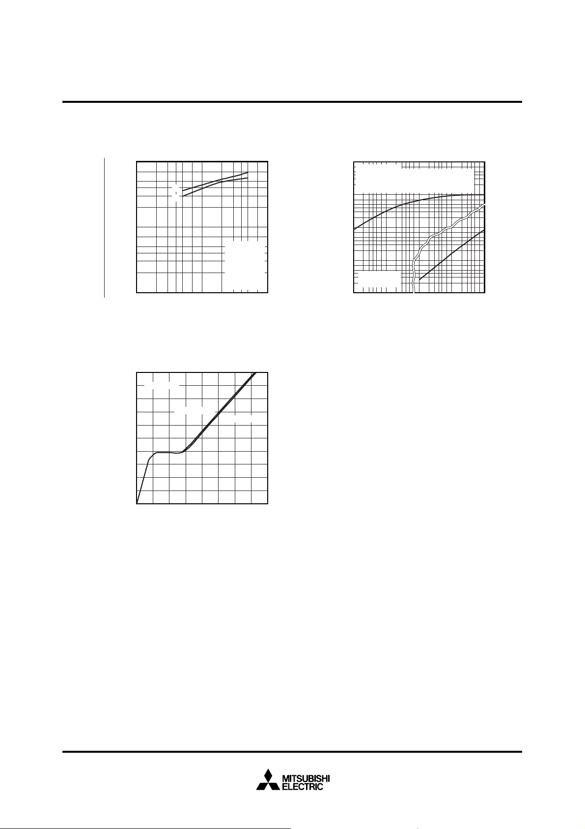
REVERSE RECOVERY CHARACTERISTICS
OF FREE-WHEEL DIODE
(TYPICAL)
2
10
(A)
rr
7
(ns)
rr
5
3
2
1
1
10
7
5
3
2
REVERSE RECOVERY TIME t
0
10
REVERSE RECOVERY CURRENT l
0
10
t
rr
I
rr
23 57
10
1
23 57
EMITTER CURRENT I
GATE CHARGE
CHARACTERISTICS
(TYPICAL)
20
(V)
GE
18
16
14
12
IC = 50A
VCC = 400V
VCC = 600V
10
8
6
4
2
GATE-EMITTER VOLTAGE V
0
0 200 400 600 800
Conditions:
V
CC = 600V
GE = ±15V
V
R
G = 6.3Ω
j = 25°C
T
Inductive load
E
(A)
10
TRANSIENT THERMAL
IMPEDANCE CHARACTERISTICS
(IGBT part & FWDi part)
10
10
10
10
10
1
3
2
–1
7
5
3
2
–2
7
5
3
2
–3
–3
–3
10
1
10
7
IGBT part:
5
Per unit base = R
3
FWDi part:
(°C/W)
2
Per unit base = R
0
10
th (j–c)
7
5
3
2
–1
10
7
5
3
2
–2
10
7
NORMALIZED TRANSIENT
5
3
2
THERMAL IMPEDANCE Z
–3
2
10
–2
23 57 23 57 23 57 23 57
10
–1
10
th(j–c)
th(j–c)
Single Pulse
T
C
= 25°C
–5
10
0
10
= 0.39°C/W
= 0.70°C/W
–4
23 57 23 57
10
TMIE (s)
GATE CHARGE QG (nC)
Aug. 1999
 Loading...