

Page 1
MITSUBISHI HVIGBT MODULES
CM1200HCB-34N
4th-Version HVIGBT (High Voltage Insulated Gate Bipolar Transistor) Modules
HIGH POWER SWITCHING USE
CM1200HCB-34N
● IC ................................................................ 1200A
● V
CES ....................................................... 1700V
● Insulated Type
● 1-element in a Pack
● AISiC Baseplate
● Trench Gate IGBT : CSTBT
● Soft Reverse Recovery Diode
APPLICATION
Traction drives, High Reliability Converters / Inverters, DC choppers
INSULATED TYPE
TM
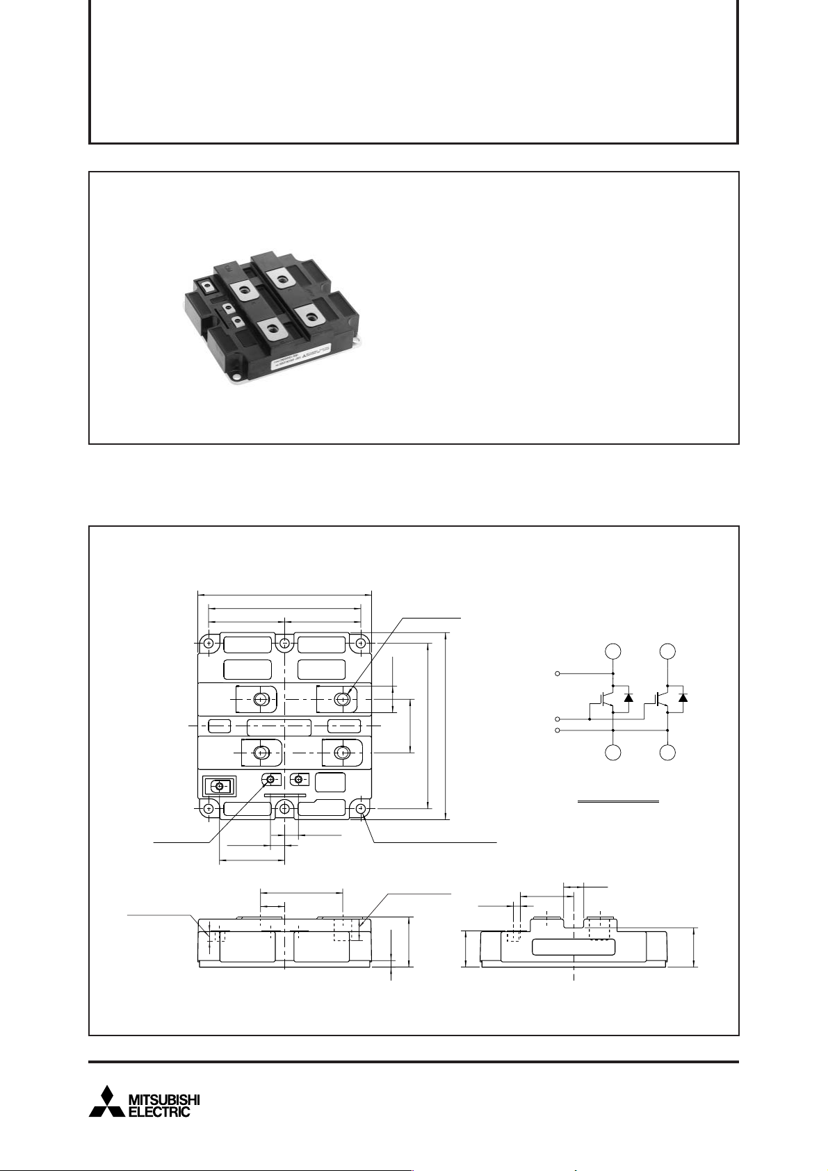
OUTLINE DRAWING & CIRCUIT DIAGRAM Dimensions in mm
130
±0.5
±0.1
3 - M4 NUTS
screwing depth
min. 7.7
CM
57
10.65
48.8
114
±0.1
C
C
E
±0.2
±0.3
18
±0.2
E
61.5
G
57
10.35
±0.3
±0.1
C
±0.2
+0.1
–0.2
20
E
6 - φ7
screwing depth
min. 16.5
±0.15
5
4 - M8 NUTS
±0.5
±0.1
±0.2
40
140
124
±0.1
MOUNTING HOLES
+1
0
38
+1
CC
C
G
E
E
CIRCUIT DIAGRAM
15
40
5.2
±0.2
0
28
±0.3
±0.2
LABEL
E
±0.5
29.5
HVIGBT (High Voltage Insulated Gate Bipolar Transistor) Modules
Sep. 2009
Page 2

MITSUBISHI HVIGBT MODULES
CM1200HCB-34N
HIGH POWER SWITCHING USE
4th-Version HVIGBT (High Voltage Insulated Gate Bipolar Transistor) Modules
MAXIMUM RATINGS
Symbol Item Conditions Ratings Unit
V
CES
V
GES
I
C
I
CM
I
E
IEM
P
c
V
iso
T
j
T
op
T
stg
t
psc
ELECTRICAL CHARACTERISTICS
Symbol Item Conditions
I
CES
V
GE(th)
I
GES
C
ies
C
oes
C
res
Q
g
V
CE(sat)
t
d(on)
t
r
E
on(10%)
t
d(off)
t
f
E
off(10%)
V
EC
t
rr
Q
rr
E
rec(10%)
Collector-emitter voltage
Gate-emitter voltage
Collector current
Emitter current (Note 2)
Maximum power dissipation (Note 3)
Isolation voltage
Junction temperature
Operating temperature
Storage temperature
Maximum short circuit pulse width
Collector cutoff current
Gate-emitter threshold voltage
Gate leakage current
Input capacitance
Output capacitance
Reverse transfer capacitance
Total gate charge
Collector-emitter saturation
voltage
Tu r n-on delay time
Tu r n-on rise time
Tu r n-on switching energy
(Note 5)
Tu r n-off delay time
Tu r n-off fall time
Tu r n-off switching energy
(Note 5)
Emitter-collector voltage
(Note 2)
Reverse recovery time
(Note 2)
Reverse recovery charge
(Note 2)
Reverse recovery energy
(Note 2), (Note 5)
VGE = 0V, Tj = 25°C
V
CE
= 0V, Tj = 25°C
DC, T
c
= 80°C
Pulse (Note 1)
DC
Pulse (Note 1)
T
c
= 25°C, IGBT part
RMS, sinusoidal, f = 60Hz, t = 1 min.
V
CC
= 1000V, VCE ≤ V
V
CE
= V
CES
, VGE = 0V
CE
= 10 V, IC = 120 mA, Tj = 25°C
V
V
GE
= V
GES
, VCE = 0V, Tj = 25°C
V
CE
= 10 V, VGE = 0 V, f = 100 kHz, Tj = 25°C
V
CC
= 900 V, IC = 1200 A, VGE = ±15 V, Tj = 25°C
I
C
= 1200 A (Note 4)
V
GE
= 15 V
V
CC
= 900 V, IC = 1200 A, VGE = ±15 V
R
G(on)
= 1.1 Ω, Tj = 125°C, Ls = 100 nH
CES
, VGE = 15V, Tj = 125°C
T
j
= 25°C
T
j
= 125°C
Tj = 25°C
T
j
= 125°C
Inductive load
CC
= 900 V, IC = 1200 A, VGE = ±15 V
V
R
G(off)
= 2.0 Ω, Tj = 125°C, Ls = 100 nH
Inductive load
E
= 1200 A (Note 4)
I
V
GE
= 0 V
CC
= 900 V, IE = 1200 A, VGE = ±15 V
V
R
G(on)
= 1.1 Ω, Tj = 125°C, Ls = 100 nH
Tj = 25°C
T
j
= 125°C
Inductive load
—
—
5.5
—
—
—
—
—
—
—
—
—
—
—
—
—
—
—
—
—
—
INSULATED TYPE
1700
± 20
1200
2400
1200
2400
8600
4000
–40 ~ +150
–40 ~ +125
–40 ~ +125
10
Limits
Ty p
—
4.0
6.5
—
220
12
3.5
15.2
2.05
2.30
—
—
0.43
—
—
0.32
2.20
1.85
—
410
0.29
MaxMin
5
10
7.5
0.5
—
—
—
—
2.70
—
1.50
0.60
—
3.00
0.60
—
3.00
—
1.50
—
—
V
V
A
A
A
A
W
V
°C
°C
°C
µs
Unit
mA
V
µA
nF
nF
nF
µC
V
µs
µs
J/P
µs
µs
J/P
V
µs
µC
J/P
HVIGBT (High Voltage Insulated Gate Bipolar Transistor) Modules
Sep. 2009
2
Page 3

4th-Version HVIGBT (High Voltage Insulated Gate Bipolar Transistor) Modules
THERMAL CHARACTERISTICS
Symbol Item Conditions
R
th(j-c)Q
R
th(j-c)R
R
th(c-f)
MECHANICAL CHARACTERISTICS
Symbol Item Conditions
M
t
M
s
M
t
m
CTI
d
a
d
s
L
P CE
R
CC’+EE’
Note 1. Pulse width and repetition rate should be such that junction temperature (Tj) does not exceed T
Thermal resistance
Thermal resistance
Contact thermal resistance
Junction to Case, IGBT part
Junction to Case, FWDi part
Case to Fin, λ
grease
= 1W/m·K, D
(c-f)
= 100 µm
M8: Main terminals screw
Mounting torque
M6: Mounting screw
M4: Auxiliary terminals screw
Mass
Comparative tracking index
Clearance
Creepage distance
Parasitic stray inductance
Internal lead resistance
2. The symbols represent characteristics of the anti-parallel, emitter to collector free-wheel diode (FWDi).
3. Junction temperature (Tj) should not exceed T
4. Pulse width and repetition rate should be such as to cause negligible temperature rise.
5. E
on(10%)
/ E
off(10%)
/ E
rec(10%)
are the integral of
T
c
= 25°C
jmax
rating (150°C).
0.1VCE x 0.1IC x dt.
opmax
MITSUBISHI HVIGBT MODULES
CM1200HCB-34N
HIGH POWER SWITCHING USE
INSULATED TYPE
Limits
19.5
32.0
rating (125°C).
—
—
—
7.0
3.0
1.0
—
600
—
—
Ty p
—
—
10.0
Limits
Ty p
—
—
—
1.5
—
—
—
15
0.21
MaxMin
14.0
21.0
—
MaxMin
13.0
6.0
2.0
—
—
—
—
—
—
Unit
K/kW
K/kW
K/kW
Unit
N·m
N·m
N·m
kg
—
mm
mm
nH
mΩ
HVIGBT (High Voltage Insulated Gate Bipolar Transistor) Modules
Sep. 2009
3
Page 4

4th-Version HVIGBT (High Voltage Insulated Gate Bipolar Transistor) Modules
PERFORMANCE CURVES
MITSUBISHI HVIGBT MODULES
CM1200HCB-34N
HIGH POWER SWITCHING USE
INSULATED TYPE
OUTPUT CHARACTERISTICS
2500
Tj = 125°C
V
GE
2000
)
A
(
1500
1000
COLLECTOR CURRENT
500
0
2500
= 20V
V
GE
= 15V
V
GE
= 12V
01 3245
COLLECTOR-EMITTER VOLTAGE (V
COLLECTOR-EMITTER SATURATION
VOLTAGE CHARACTERISTICS
V
GE
= 15V
(
TYPICAL
(
TYPICAL
)
V
GE
V
)
GE
= 10V
= 8V
)
TRANSFER CHARACTERISTICS
2500
V
CE
= 20V
2000
)
A
(
1500
1000
COLLECTOR CURRENT
500
Tj = 25°C
T
j
6
0
02 64810
2500
= 125°C
GATE-EMITTER VOLTAGE (V
FORWARD CHARACTERISTICS
(
TYPICAL
FREE-WHEEL DIODE
(
TYPICAL
)
)
12
)
2000
)
A
(
1500
1000
COLLECTOR CURRENT
500
Tj = 25°C
j
= 125°C
T
01234
COLLECTOR-EMITTER SATURATION VOLTAGE (V
HVIGBT (High Voltage Insulated Gate Bipolar Transistor) Modules
2000
)
A
(
1500
1000
EMITTER CURRENT
500
Tj = 25°C
T
j
00
01234
)
4
EMITTER-COLLECTOR VOLTAGE (V
= 125°C
)
Sep. 2009
Page 5

4th-Version HVIGBT (High Voltage Insulated Gate Bipolar Transistor) Modules
MITSUBISHI HVIGBT MODULES
CM1200HCB-34N
HIGH POWER SWITCHING USE
INSULATED TYPE
CAPACITANCE CHARACTERISTICS
3
10
7
5
3
2
)
2
10
nF
(
7
5
3
2
1
10
CAPACITANCE
7
5
3
V
GE
= 0V, Tj = 25°C
2
f = 100kHz
0
10
-1
23 57
10
COLLECTOR-EMITTER VOLTAGE (V
HALF-BRIDGE SWITCHING ENERGY
1.8
V
CC
= 900V, V
R
G (on)
1.6
Tj = 125°C, Inductive load
1.4
)
J/P
(
1.2
(
TYPICAL
0
23 57 23 57
CHARACTERISTICS
(
TYPICAL
GE
= 1.1Ω, R
= ±15V
G (off)
= 2.0Ω
)
GATE CHARGE CHARACTERISTICS
(
TYPICAL
)
20
V
CE
= 900V, IC = 1200A
Tj = 25°C
15
)
V
C
ies
(
10
5
0
C
oes
-5
GATE-EMITTER VOLTAGE
-10
C
10
res
1
10
2
)
-15
051015 2010
GATE CHARGE (µC
)
HALF-BRIDGE SWITCHING ENERGY
)
CHARACTERISTICS
(
TYPICAL
)
3.5
V
CC
= 900V, IC = 1200A
V
GE
= ±15V, Tj = 125°C
Inductive load
3.0
E
on
)
J/P
(
2.5
E
on
1.0
0.8
E
off
0.6
SWITCHING ENERGIES
0.4
E
rec
0.2
0
0 500 1000 1500 2000 2500
COLLECTOR CURRENT (A
HVIGBT (High Voltage Insulated Gate Bipolar Transistor) Modules
)
2.0
1.5
1.0
SWITCHING ENERGIES
0.5
0
024681012
5
GATE RESISTANCE (Ω
E
off
E
rec
)
Sep. 2009
Page 6

4th-Version HVIGBT (High Voltage Insulated Gate Bipolar Transistor) Modules
MITSUBISHI HVIGBT MODULES
CM1200HCB-34N
HIGH POWER SWITCHING USE
INSULATED TYPE
HALF-BRIDGE SWITCHING TIME
1
10
V
CC
= 900V, V
7
R
G (on)
5
3
2
= 1.1Ω, R
T
j
= 125°C, Inductive load
t
d(off)
)
µs
0
10
(
10
SWITCHING TIMES
10
t
d(on)
7
5
3
2
-1
7
5
3
2
-2
10
t
f
t
r
2
COLLECTOR CURRENT (A
CHARACTERISTICS
(
TYPICAL
GE
= ±15V
G (off)
= 2.0Ω
3
10
)
FREE-WHEEL DIODE REVERSE RECOVERY
CHARACTERISTICS
(
2
10
V
CC
= 900V, V
7
R
G (on)
5
3
)
2
µs
(
1
10
7
5
3
2
0
10
7
5
REVERSE RECOVERY TIME
3
2
-1
10
4
423 57423 57
10
10
= 1.1Ω, Tj = 125°C
Inductive load
2
)
TYPICAL
GE
= ±15V
EMITTER CURRENT (A
10
)
l
rr
t
rr
3
423 57423 57
10
4
10
7
5
)
3
A
(
2
3
10
7
5
3
2
2
10
7
5
REVERSE RECOVERY CURRENT
3
2
1
10
4
)
TRANSIENT THERMAL IMPEDANCE
CHARACTERISTICS
1.2
R
th(j–c)Q
= 14.0K/kW
R
th(j–c)R
= 21.0K/kW
1.0
0.8
0.6
0.4
0.2
NORMALIZED TRANSIENT THERMAL IMPEDANCE
0
10
-3
23 57
10
-2
23 57
TIME (s
10
-1
23 57
)
10
0
23 57
10
1
HVIGBT (High Voltage Insulated Gate Bipolar Transistor) Modules
Sep. 2009
6
Page 7

4th-Version HVIGBT (High Voltage Insulated Gate Bipolar Transistor) Modules
REVERSE BIAS SAFE OPERATING AREA
6000
V
CC
≤ 1200V, V
T
j
= 125°C, R
5000
)
A
(
4000
3000
2000
COLLECTOR CURRENT
1000
GE
G (off)
(
RBSOA
= ±15V
≥ 2.0Ω
)
25000
CC
≤ 1000V, V
V
R
G (on)
≥ 1.1Ω, R
j
= 125°C, tpsc ≤ 10µs
T
20000
)
A
(
15000
10000
COLLECTOR CURRENT
5000
MITSUBISHI HVIGBT MODULES
CM1200HCB-34N
HIGH POWER SWITCHING USE
INSULATED TYPE
SHORT CIRCUIT
SAFE OPERATING AREA
(SCSOA)
GE
= ±15V
G (off)
≥ 2.0Ω
0
0 500 1000 1500 2000
COLLECTOR-EMITTER VOLTAGE (V
FREE-WHEEL DIODE REVERSE RECOVERY
SAFE OPERATING AREA
(
)
RRSOA
1600
V
CC
≤ 1200V, di/dt ≤ 6500A/µs
Tj = 125°C
1400
)
A
(
1200
1000
800
600
400
REVERSE RECOVERY CURRENT
200
0
0 500 1000 1500 2000
)
COLLECTOR-EMITTER VOLTAGE (V
)
0
0
HVIGBT (High Voltage Insulated Gate Bipolar Transistor) Modules
500 1000 1500 2000
COLLECTOR-EMITTER VOLTAGE (V
)
Sep. 2009
7
 Loading...