

Page 1
Page 2

REVISIONS
*The
*Mtanual
IB
(NA)
66593-A
Number
First
edition
Page 3

Page 4
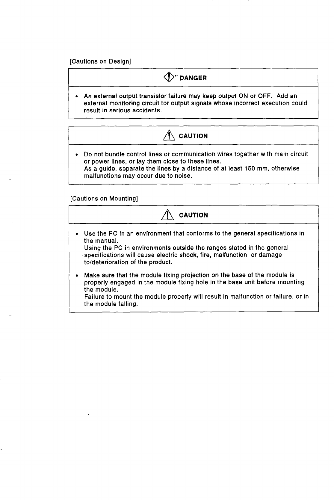
[Cautions on Design]
0''
I
0
An
external output transistor failure may keep
external monitoring circuit for
result
0
Do not bundle control lines or communication wires together with main circuit
or power lines, or lay them close
As a guide, separate the lines by a distance of at least
malfunctions may occur due
[Cautions on Mounting]
0
Use
the manual.
Using the PC in environments outside the ranges stated
specifications will cause electric shock, fire, malfunction, or damage
to/deterioration of the product.
in
serious accidents.
A
the PC in an environment that conforms
DANGER
output
A
CAUTION
to
to
noise.
CAUTION
output
signals whose incorrect execution could
these lines.
to
ON
or
OFF.
150
mm, otherwise
the general specifications in
in
the general
Add an
0
Make
sure that the module fixing projection on the base of the module is
properly engaged in the module fixing hole in the base unit before mounting
the module.
Failure
the module falling.
to
mount the module properly will result in malfunction or failure, or in
Page 5
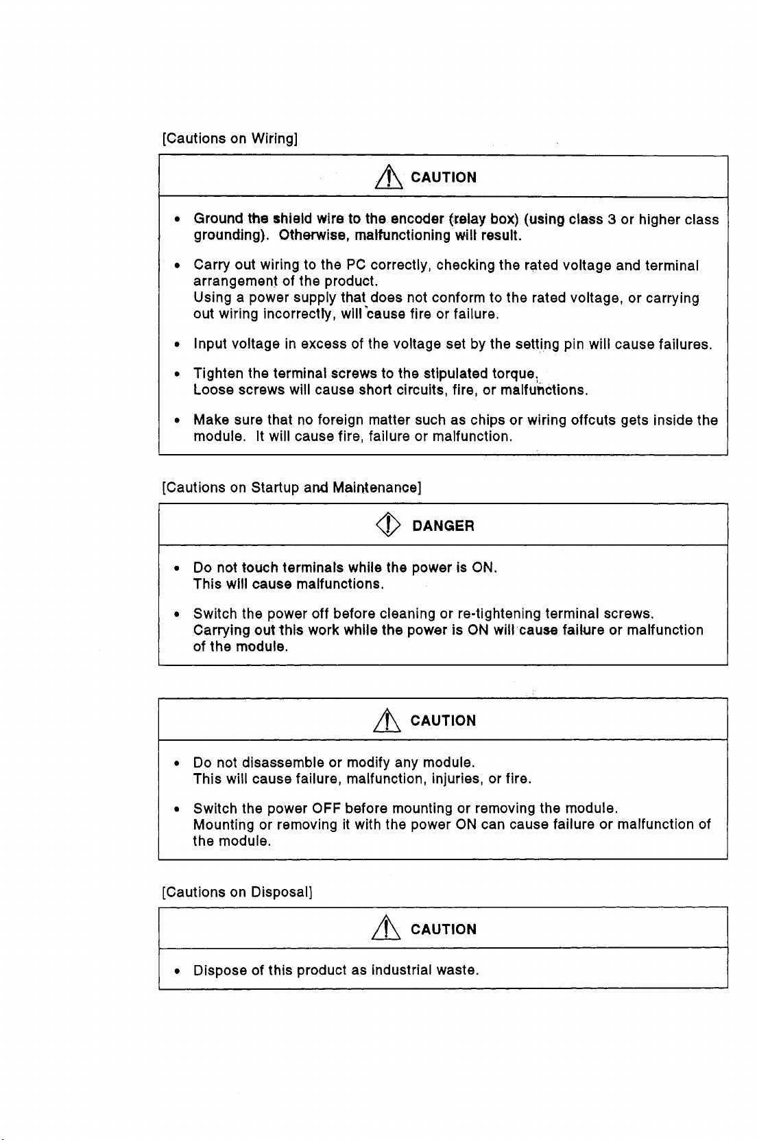
[Cautions on Wiring]
Q
1
CAUTION
Ground
grounding). Otherwise, malfunctioning
Carry out wiring
arrangement of the product.
Using a power supply that does not conform
out wiring incorrectty, will *cause fire or failure.
Input voltage in excess of the voltage set
Tighten the terminal screws
Loose
Make sure that no foreign matter such as chips or wiring offcuts gets inside
module.
[Cautions on Startup and Maintenance]
Do
This
Switch the power off before cleaning or re-tightening terminal screws.
Carrying out
of the module.
he
shield wire to the encoder
to
screws will cause
It
will
cause fire, failure or malfunction.
not
touch
terminals while the power is
will
cause malfunctions.
this
work while the power is
@lay
the PC correctly, checking the rated voltage and terminal
to
the stipulated torque.
short
circuits, fire, or malfukctions.
@
DANGER
box)
(using class 3 or higher class
wilt
result.
to
the rated voltage, or carrying
by
the setting pin will cause failures.
ON.
ON
will cause failure or malfunction
the
A
CAUTION
Do
not disassemble or modify any module.
This will cause failure, malfunction, injuries, or fire.
Switch the power
Mounting or removing
the module.
[Cautions on Disposal]
Dispose of this product as industrial waste.
OFF
before mounting or removing
it
with the power
A
CAUTION
ON
the
module.
can cause failure or malfunction of
Page 6

INTRODUCTtON
Thank you for choosing the Mitsubishi MELSEC-A Series
lers. Please read this manual carefully
to
manual should be forwarded
the end User.
so
that the equipment
of
General Purpose Programmable Control-
is
used
to
its
optimum. A copy
of
this
,
..
.
Page 7
1 . INTRODUCTION
.......................................................
..
1-1-1-2
1.1 Features
2
.
SYSTEM
3
.
SPECIFICATIONS
3.1 General Specifications
3.2 Performance Specifications
3.3 Functions
3.4 Interfaces with External Devices
3.5 I/O Signals fromho the PC CPU
3.6 Buffer Memory Allocation
3.7 Applicable Encoders
4 . INSTALLATION AND PRE-OPERATION SElllNG PROCEDURE
4.1 Pre-Operation Setting Procedure
4.2 Handling Precautions
4.3 Part Names and Settings
4.4 Wiring
CONFIGURATION
4.4.1 Wiring preconditions
4.4.2 Wiring example for the connection with the open collector
4.4.3 Wiring example for the connection of a controller
4.4.4 Wiring examples at external output terminals
................................
:
..............................
............................................
..................................................
..................................................
...............................................
.............................................................
...........................................
...........................................
...............................................
...................................................
..........................................
....................................................
................................................
...............................................................
..............................................
output pulse generator
input terminals (PRESET and FSTART)
............................................
to
external
.............................
(EQUs
1
2 . 1 . 2 . 1
-3-
.............
to
2)
..............
4 . 1
1
- 3 -
.
1 - 2
12
3
-
1
3 - 2
3-5
3 - 6
3
-
9
3 - 11
3 - 12
4 . 12
4 - 1
4 - 2
4 - 3
4-7
4
-
7
4
-
8
4 - 11
4 - 12
5 . PULSE INPUTANDCOUNTING METHOD
5.1
Single-phase Pulse Input
5.2 Counting at 2-Phase Pulse Input
5.3 Reading the Present Value
6
.
EXECUTING THE COINCIDENCE OUTPUT FUNCTION
6.1 Coincidence Output Function
6.1.1 Coincidence output function operation
6.1.2 Program examples
7
.
EXECUTING THE PRESET FUNCTION
7.1 PresetFunction
7.2 Preset Using the Sequence Program
7.2.1 Executing the preset function using the sequence program
7.2.2 Example program
7.3 Preset
7.3.1 When the preset is executed
by
........................................................
External Input
................................................
...............................................
.............................................
...............................................
................................................
.................................................
.................................
...........................................
..................................
.......................................
by
external control signal
5-1
-5-8
5
-
3
5
-
4
5
-
5
......................
................................
................
...................
6
. 1 . 6 .
7
. 1 . 7 .
6
6
-
1
6 - 2
6 - 3
11
7-1
7 - 2
7 - 2
7 - 3
7 - 7
7 - 7
Page 8
8
.
EXECUTING
8.1
Ring Counter Functio’n
8.1.1
8.1.2
8.2
Example Program
9
.
SELECTING ‘AND EXECUTlNG THE
9.1
Selecting. a Counter Function
9.1.1
9.1.2
9.2
Count Disable Function
9.2.1.
9.3
Latch Counter Function
9.3.1
9.4
Sampling Counter Function
9.4.1
9.5
Periodic Pulse Counter Function
9.5.1
THE
RING
COUNlERFUWTlffl
I-
Ring counter function operation
Countrange
......................................................
Reading the counter function selection count value
Counterrors
Example program
Example
Example program
Example program
program
...........
.............................
...........
....................................................
...............................................
....................................................
..................................................
................................................
..............
...............................................
..............................................
...............................................
...............................................
,
......................................
.....................................
COUMZR
FUNCTION
.................
......................
...
..................................
..........................................
..........
8
9
.
7
-
1
. 8 .
8
8
8-3
8
.
1
.
9
.
9 -1
9
9-6
9
9
9 - 12
9 - 13
9 - 17
9 - 18
9 - 22
9 - 24
.8
8
-1
-2
-5
27
-3
-7
-8
10 . PRO.GR.4MMING
A
REMO=’I~O
11.1
Errorlnformation
Counter Value is Incorrect
1 1.2
11.3
Count Cannot be Made
APPENDIX 1 PERFORMANCE COMPARISON BETWEEN THE
THE
APPENDIX 2 EXTERNAL DIMENSIONS
FOR
STATION
AlSD61.
USING THE AlSD62(ElD) WITH
............................................
......................................................
...............................................
.................................................
AlSD62(E/D).
AND THE AD61
(Sl)
...................................
.........................................
.IO
- I -
IO
11-1
11
11 - 2
APP
APP
-
-
.
.
3
2
1
3
Page 9
1
INTRODUCTION
1.
INTRODUCTION
MELSEC-A
This user’s manual describes
ming of
(hereinafter called the AlSD62(E/D))
MELSEC-A series CPU module (hereinaftei called the PC CPU).
The AlSD62, AlSD62E and AlSD62D are a Dq-inpupsink output type, a
DC input source output type and a differential ,input sink output type, respectively.
The maximum
(A1 SD62D).
The A1 SD62(OD) counts single-phase and 2-phase pulse inputs as shown
below:
the
Al-SD62/Al
counting
Single-phase pulse input multiplied by one
.........
Counts at the leading
Single-phase pulse input multiplied by
.........
Counts at the leading edge and trailing edge of the pulse.
2-phase pulse input multiplied by one
........
,Counts at the leading edge or trailing edge of the phase
pulse.
2-phase pulse input multiplied by two
the
spsqifications, handling and prqqrgm-
&fZWAfSb62D
speed
ia
100
kpps
type
to
be-used
(A,ISD62(E))
edge
two
htgh-s$&d
in
combination with a
or
trailing edge of the pulse.
eounter thbdute
or
200
kpps
A
.........
Counts
pulse.
2-phase pulse input multiplied by four
.........
Counts at the leading edge and trailing edge of the phase
and phase B pulses.
at
the
leading edge and trailing edge
of
the phase
A
A
1-1
Page 10
1.
INTRODUCTION
MElSEC-A
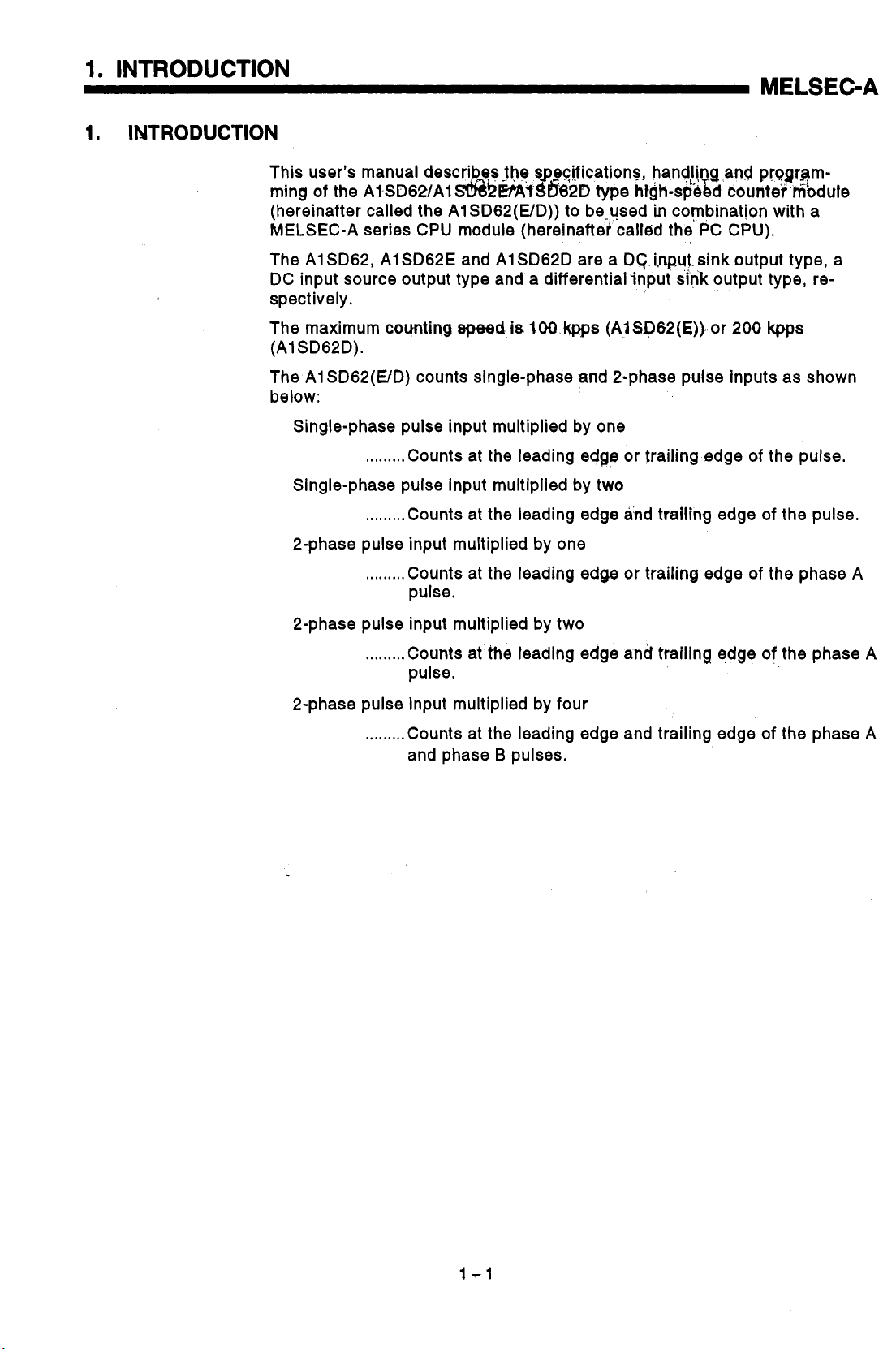
The following diagram outlines how the AlSD62(E/D) operates.
(4)
I/O
signal
bufbr memory
A1 SD62
A1 SD62E
Ai SD62D
(1
1
CHI
(2)
.
(3)
Coincidence
output
(2
points)
function selection
Pulse
generator
I
Encoder
8
I
Controller
(1) Input pulses to the
(2)
The preset or counter function can
(3)
The pulse
and a slgnat is Issued accordlngly.
(4)
The sequence pro ram helps confirm the
A1
preset the counter.
I
,
I
SD62IAlSD628AI SD620
Pulse
m
External control
signal
-
Pmset/Counter
function selection
A1 SD62/A1 SD62WA1 SD62D
is
compared as a coincidence output with the present count value,
rn
and
______.
(1
1
CH2
are counted.
be
selected with an external control signal.
I/O
the
buffer
signals
rhemory
of
status, and start, stop and
~
the
(3)
Coincidence
output
(2
points)
1-2
Page 11
1.1
Featuree
The following are the features of the AlSD62(E/D):
Pulses can be counted in a wide range from
The count value is stored in 24-bit binary.
The count value can be multiplied
Multiplication
inputs, or multiplication
The maximum counting speed can
4.3).
Since a maximum cogoting speed of either
selected with the
accurate pulse counting
ing edge.
Coincidence output .is available
ON/OFF signals are issued according
preset output status of a selected channel and the present counter value.
One
module can accept two inputs, and issues
which can
A
ring counter function
Counting repeats between the preset value and the ring counter value,
and this function
by
either one or two can
by
one, two
AlI8D62(E),
is
possible even with a slow leading edgehail-
serh
as upper and lower limit signals.
is
available
is
effective
(see
be
or
be
or
200 kpps or
(see
Section 6).
(see
in
contrdling fixed-pitch feed.
0
to
1677721
Section
selected for single-phase pulse
four for 2-phase pulse inputs.
switched (see Sections 3.2 and
,.
to
Section
5).
100
kpps or 10 kpps can be
10
kpps with the A1 SD62D,
the
comparison between the
two
outputs
8).
5.
to
one input,
Four counter functions are selectable
One of the following functions can be selected and used:
(a) Latch counter function
(b)
Sampling counter function
(c) Periodic pulse counter function
(d) Count disable function
The preset or counter function can
signal
By
external terminal, the preset or counter function, respectively, can be
executed.
These functions can be used
(see
Section 7.3 and Section
applying voltage to the PRESET (preset) or F.START (function start)
.....................
..............
.....................
to
(see
Section
Latches the present counter value
in response
Counts the incoming pulses within
the preset period of time from
signal input.
......
Stores the present and revious
counter values at prese P Intervals
during signal input.
Stops pulse counting with an input
signal while the count enabled
command is executed.
be
selected with an external control
9).
eliminate the influence of scan time.
9).
to
an input signal.
n
1-3
Page 12
2.
SYSTEM
..
'
,
2.
SYSTEM
CONFIGURATION
-
CONFIGURAVON
(1) Appilcable CPUs
*A1 SJCPU(S3) *A1 SCPU(S1) *A2SCPU(S1) *A2ASCPU(Sl/S30)
*A5GCPU(T21 B) *A1 SCPUC24-R2
(2) Number mountable
MELsEGA
Any number of modules can be used, provided the number of
of
the
appilcable CPU is not exceeded.
(3) Available
Any
slots
slot
in the base unit can be used, provided the following considera-
tion is not a problem.
When mounting modules in an extension base unit that does not have
power supply (A1 S52B(S1), A1 S55B(S1), A1 S58B(S1)),
the
power supply capacity may be insufficient.
When mounting an AlSD62(E/D)
to
an extension base unit, and exten-
sion base unit after carefully considering the following factors:
the
1) Current capacity of
power supply module on the main base
unit
2) Voltage drop at
3) Voltage drop
the
main base unit
at
the extension base unit
4) Voltage drop in the extension cable
(4)
Data link system
In a data link system, the module can be mounted at a master station,
local station, or remote
station program, refer
I/O
station. For an example of a remote
to
the MELSECNET, MELSECNET/B
System Reference Manual.
I/O
Data
points
a
I/O
Link
For Details on the ranges for the number of
to the following manuais:
A1 SJCPU (S3) User's Manual
AlS/AlSC24-FWMSCPU
APASCPU (Sl/SSO)
A52GCPU (T21
User's
8)
User's Manual
.........................................................
User's
Manual
Manual
................................................
....................................................
2-1
I/O
points, and on calculating voltage drops, refer
18-66446
.....................................
18-66320
18-66268
18-6641
9
Page 13
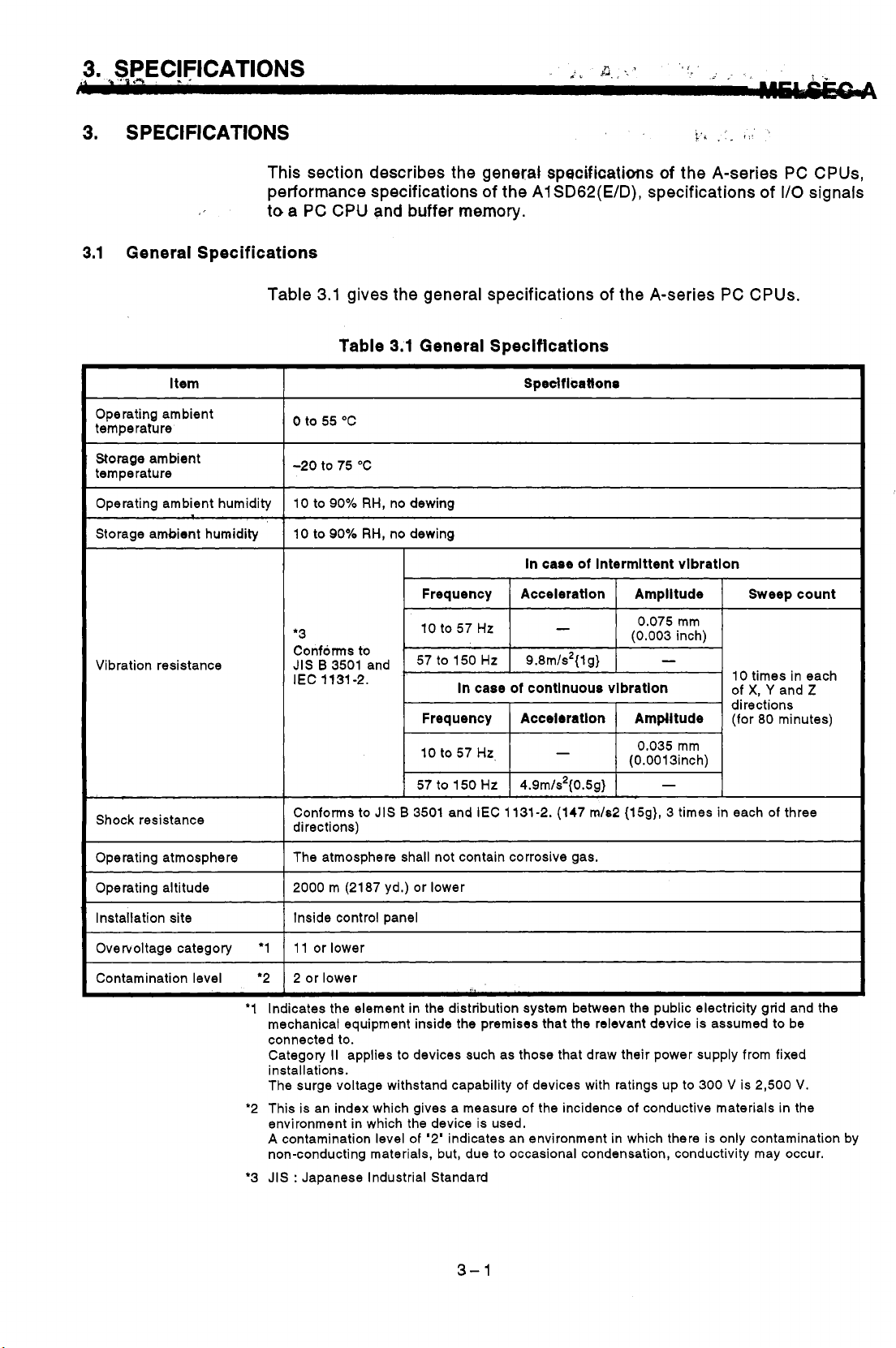
3.
SPECIFICATIONS
3.1
General Specifications
Item
Operating ambient
temperature
Storage
temperature
Operating ambient humidity
Storage ambient humidity
Vibration resistance
Shock resistance
ambient
This section describes the general specifications
the
performance specifications of
to
a
PC
Table
0
to
-20
10
-
10
'3
Conforms
JIs
IEC
Conforms
directions)
CPU and buffer
3.1
gives
the
Table
55
to
75 "C
to
90% RH, no dewing
to
90%
B
3501
1131-2.
3.1
"C
RH,
no dewing
to
and
to
JIS B 3501 and IEC 1131-2. (147
memory.
general specifications
General Specifications
Frequency
to
150
In case
to
57
to 150
HZ
Hz,
HZ
57
Frequency
10
57
AlSD62(E/D), specifications of
of
the
A-series PC CPUs.
Spedflcattone
In case
Acceleration
I
I
9.8m/s2{lg}
of
continuous vibration
Acceleration
4.9m/s2{0.5g)
of
lntermlttent vibratlon
Amplitude
1
Amplitude
-
0.035
(0.0013inch)
m/s2
{lsg}, 3 times in each of three
of
the A-series PC CPUs,
I/O
signals
Sweep count
-
10 times in each
of
X,
Y
and
directions
(for
80
mm
-
2
minutes)
Operating atmosphere
Operating altitude
Installation site
Overvoltage category '1
Contamination level '2
*l
'2
'3
The atmosphere shall not contain corrosive gas.
2000 m (2187 yd.) or lower
Inside control panel
11 or lower
2 or lower
~~
Indicates the element in the distribution system between the public electricity grid and the
mechanical equipment inside
connected
Category
installations.
The surge voltage withstand capability of devices with ratings up
This is an index which gives a measure of the incidence of conductive materials in the
environment in which the device is used.
A
contamination level of
non-conducting materials, but, due
JIS : Japanese Industrial Standard
to.
II
applies to devices such as those that draw their power supply from fixed
the
premises that the relevant device is assumed
to
300
'2'
indicates an environment in which there is only contamination by
to
occasional condensation, conductivity may occur.
V
is
2,500
to
be
V.
3-1
Page 14
3.
SPECIFICATIONS
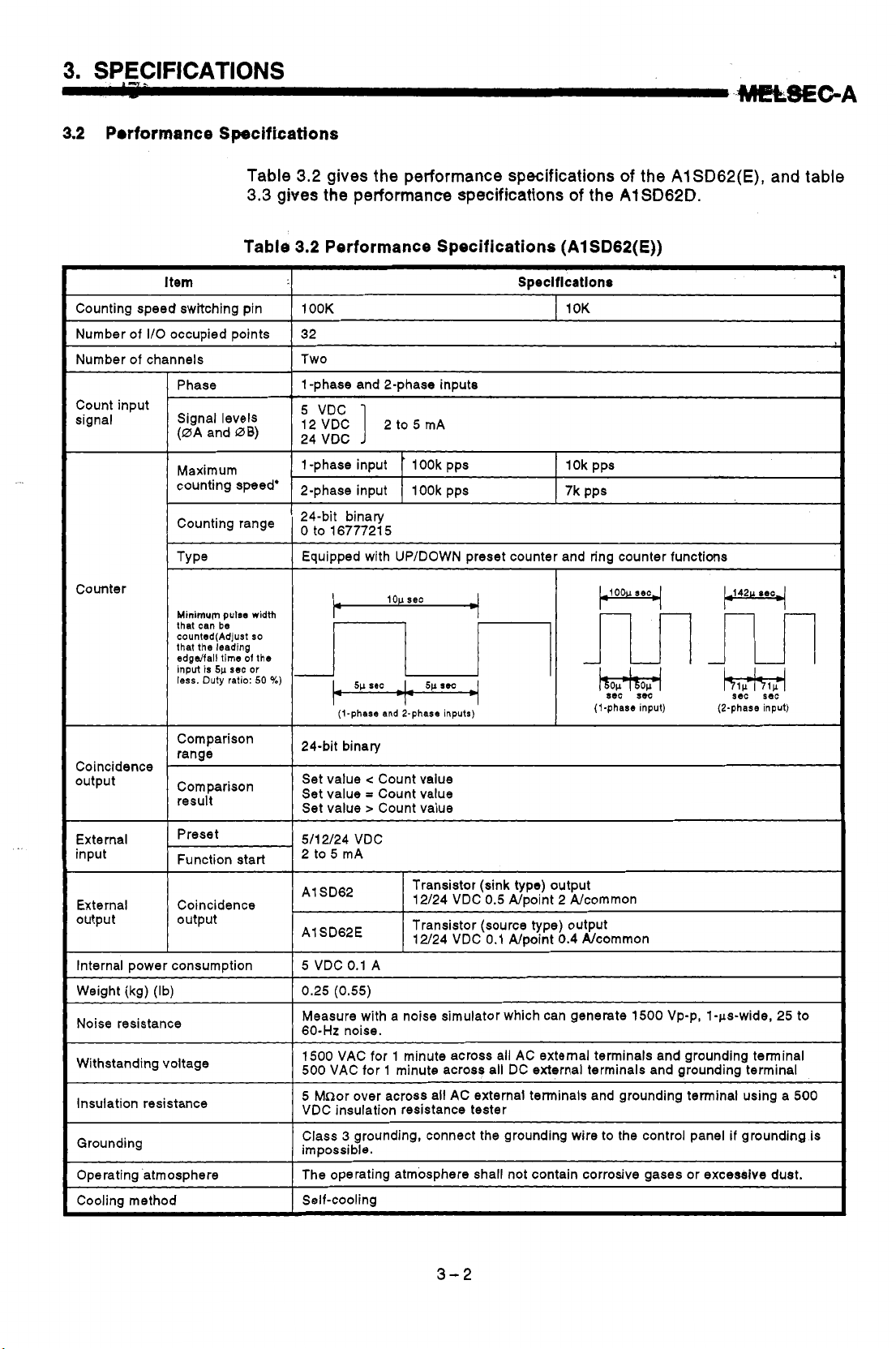
3.2
Porformance Specifications
...-----
c.
Table
3.3
Table
Item
Counting speed switching pin
I/O
occupied points
Number of channels
Phase 1 -phase and 2-phase inputs
Count input
signal
Maximum 1 -phase input 1 OOk pps
counting
I
TY
Counter
'ped'
Pe Equipped with UP/DOWN preset counter and ring counter functions
3.2
gives the performance specifications of the
gives
the performance specifications of the
3.2
Performance Specifications
1
OOK
32 Number of
I
Two
2-phase input
1 OOk pps 7k PPS
top
sec
(AlSD62(E))
Speclflcatlonr
1
OK
~ ~ ~~ ~~~
10k pps
AlSD62(E),
AlSD62D.
~ ~ ~ ~ ~~~~~~
and table
I
edgdfall
time
is
5p
input
less.
sec
Duty ratio:
I
Coincidence
output
External
input
External
output
Internal power consumption
Weight (kg) (Ib)
Noise resistance
Withstanding voltage
Insulation resistance
Grounding
Operating atmosphere
Cooling method
Comparison
result
Coincidence
t
output
L
of
the
or
50
%)
Set value
Set value
Set value
A1 SD62
A1 SD62E
5
0.25
Measure with a noise simulator which can generate 1500 Vp-p, 1-ps-wide, 25
60-Hz
1500 VAC for
500
5
VDC insulation resistance tester
Class 3 grounding, connect the grounding wire
impossible.
The operating atmosphere shall not contain corrosive gases or excesslve dust.
I
Self-cooling
5p
sec
(t-phase and 2-phase inputs)
<
Count value
=
Count value
>
Count value
Transistor (sink type) output
12/24 VDC
Transistor (source type) output
12/24 VDC 0.1 Npoint 0.4 Ncommon
VDC
0.1
A
(0.55)
noise.
1
VAC for 1 minute across all DC external terminals and grounding terminal
Mnor over across all AC external terminals and grounding terminal using a
minute across all AC external terminals and grounding terminal
0.5
Npoint 2 Ncommon
(I-phase input) (?-phase input)
~ ~ ~~~ ~~~ ~ ~
to
the control panel
if
grounding is
to
500
3-2
Page 15
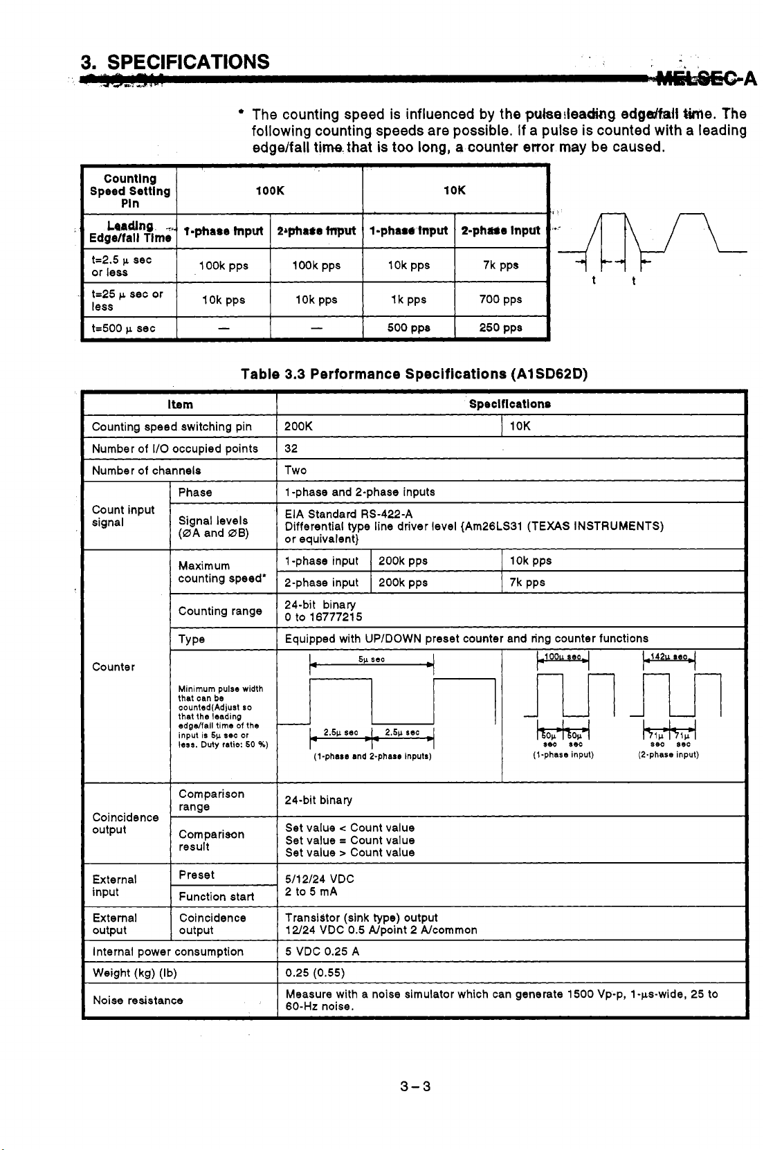
3.
SPECIFICATIONS
*A
,
.i.;
.
The
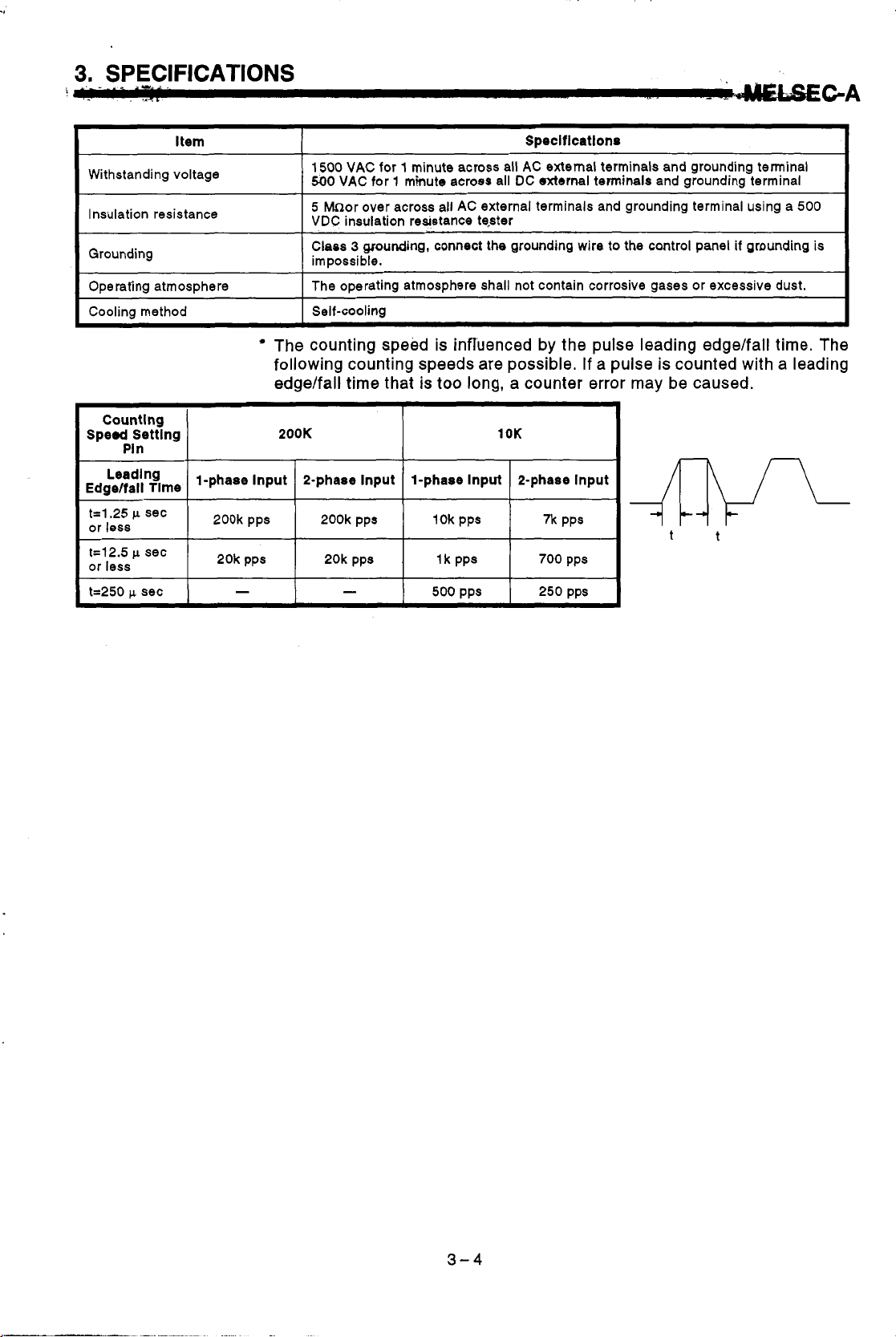
counting speed is influenced
by
the
puketleaag
following counting speeds are possible. If a pulse
edge/fall
timathat
is
too
long,
a
counter error may
I.
edgedfait
is
counted with a leading
be
caused.
me.
The
Countlng
Speed
Settlng
Pin
Edgelfall
k2.5 p sec
or less
t=25
less
t=500 p sec
Tlmo
sec or
f=phare
1
OOk pps
1
Ok pps
-
tnput
-'-
Table
Item
Counting speed switching pin
Number of
Number of channels
Count input
signal
Counter
I/O
occupied points
Phase
Signal levels
(0A and 0B)
Maximum
counting speed'
Counting range
TY
Pe
Minimum pulse width
that can
be
counted(Adjust
that the leading
edgdfall time
input is
5p
less.
Duty
sec
ratio:
of
or
so
the
50
1
%)
OOK
1
OK
Pq~ha$o
Input
1 OOk pps
1 Ok pps
-
3.3
Performance Specifications
1-pharr.tnput
1
k PPS
500
Pps
2-ph-e Input
7k PPS 1 Ok pps
700 pps
250
pps
(A1
t t
SD62D)
Speclflcatlons
OK
200K
32
Two
1 -phase and 2-phase inputs
EIA Standard RS-422-A
Differential type line driver level {Am26LS31 (TEXAS INSTRUMENTS)
or equivalent}
1 -phase input 200k pps
2-phase input 200k pps
24-bit binary
0
to 1677721
Equipped with UPIDOWN preset counter and ring counter functions
5
(I-phara and 2-phase inputs)
1
1 Ok pps
7k
PPS
(1-phase input)
(2-phase input)
b142u
s6c
aecd
sac
Comparison
Coincidence
output
External
input
External
output
Internal power consumption
Weight (kg) (Ib)
Noise resistance
range
Comparisan
result
Preset
Function start
Coincidence
output
~~ ~
24-bit binary
Set value
Set value
Set value
5/12/24 VDC
2to5mA
Transistor (sink type) output
12/24 VDC
5
VDC 0.25 A
0.25
Measure with a noise simulator which can generate 1500 Vp-p, 1-ps-wide, 25
60-Hz
(0.55)
noise.
<
Count value
=
Count value
>
Count value
0.5
Npoint 2 Ncommon
3-3
to
Page 16
3.
SPECIFICATIONS
!-
-GA
Withstanding voltage
I
Insulation resistance
I
Grounding
~~ ~~ ~~ ~~
Operating atmosphere
I
Coolina method
,
-.
.e
~
Item
I_
~
Speclficatlons
1500
VAC
500
5 Mor over across all
VDC
Class
impossible.
The operating atmosphere shall not contain corrosive gases or excessive dust.
I
Self-coolins
for 1 minute across all
VAC
for 1 minute acroas all
insulation resistance te-ster
3
grounding, connect
.~~
.
AC
AC
external terminals and grounding terminal
DC
sxternal
external terminals and grounding terminal using a 500
the
grounding wire to the control panel
terminals
~~ ~~ ~
and grounding terminal
1
if
grounding is
I
I
I
I
Counting
Sped Setting
n
PI
Edge,fal,
Leading
t=l.25 p sec
or less
k12.5
p
or less
t=250 p sec
t
sec
1-phase
200k
The counting speed is influenced
following counting speeds are possible.
edge/faII
200K
Input
pps
time
that
2-phase Input
200k pps
is
too
long, a counter error may be caused.
1-phase Input
1
Ok pps
1
k PPS 20k pps 20k pps
- -
by
1
OK
2-phase input
700
250
the pulse leading edge/fall time. The
If
PPS
7k
pps
pps 500 pps
a pulse
is
counted with a leading
t t
3-4
Page 17
$3.3
:.A
--
Functions
,1
.
',
Functtan
,.
FOincideQCe.,QUtpIJt function
Preset
Ring counter
Count disable'
Latch counter
Counter
function
selection
function
Periodic pulse
counter
counter
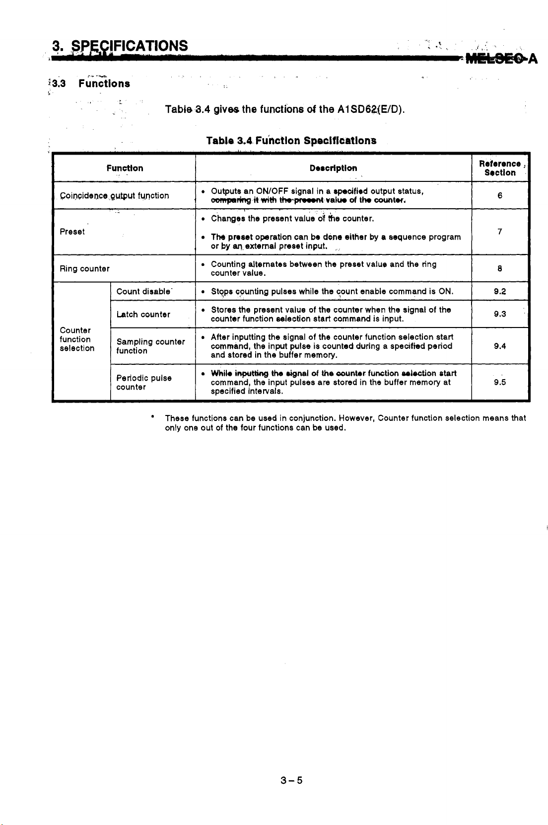
Table-3.4
Table
gives
the
functions
3.4.
functlon
of
the
AlSDGZ{E/D).
SpecUlcatlons
Descflptlon
Outputs an ON/OFF signal in a $pacified output status,
Changes the present value
The
pnset operation can be
or by
w.
external
Counting alternates between
counter value.
Stqps
counting pulses while the qount enable command is ON.
Stores
the
counter function selection start command is input.
After inputting the signal of the counter function selection start
command, the input pulse is counted during a specified period
stored
and
While
inputting
command, the input pulses are stored in the buffer memory at
specified intervals.
preset
present value of
in
the buffer memory.
the
signal
d
input.
the
of
done
the
he
counter.
either
,
the
counter when
aounter
by a sequence program
preset value and the ring
the
function
signal
of
eaJoction
the
start
Reference
Section
7
8
9.2
9.3
9.4
9.5
These functions can be used in conjunction. However, Counter function selection means that
only one out of the four functions can be used.
3-5
Page 18
3.
S.PECIFICATIONS
..
r
3.4
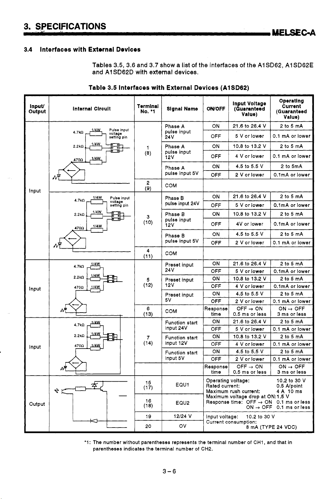
Interfaces with External
EIGA
Devices
Input/
output
Input
Input
Input
output
I
I
I
Tables 3.5, 3.6 and 3.7
and AlSD62D
Table
internal Clrcult
I
2.2k0
I
4.7kn
I
4.7k0
fi
show
a list
of
the
interfaces
with
external devices.
3.5
Interfaces with External Devices (AlSD62)
Input Voltage
Pulse input
voltage
setting pin
I
'yr\!'
19)
\-I
111)
(1 3) time 0.5
7
(1 4) input
15 EQU1 Operating voltage:
7)
(1
Signal
Name
Phase A
pulse input
I
*4v
Phase A
pulse input
12v OFF 4 V or lower 0.1 mA or lower
Phase A
pulse input
I
COM
,
Phase
B
pulse input
Phase
B
pulse input
12v OFF 4V or lower O.lmA or lower
Phase
B
pulse input
I
COM
1
COM
Function
input 24V
Function start
Function start
input 5V
start
12V
OWOFF
- -
ON
OFF 5
ON
ON
5v
24v
5v
OFF 2 V or lower O.lmA or lower
I
I
ON
OFF 5 V or lower 0.1 mA or lower
ON
ON
OFF 2 V or lower 0.1 mA or lower
ON
OFF
ON
OFF
ON
OFF
Response OFF
ON
OFF
ON
OFF
ON
OFF 2 V
Response OFF
time
Rated current: 0.5 Npoint
Maximum rush current: 4A 10ms
Maximum voltage drop
Response timer OFF'+
(Guaranteed (Guaranteed
~ ~ ~~~~
21.6
10.8
4.5
~~ ~~
21.6
10.8 to 13.2 V 2
4.5
I
21.6
I
5 V or lower
I
10.8
I
4 V or lower
I
4.5
I
2
21.6
5
10.8
4
4.5
0.5
I
Input voltage: 10.2 to
Current consumption:
of
the
Ai
SD62,
Value)
to
26.4
V
V
or lower 0.1 mA or lower
to
13.2 V 2
to
5.5
v
to
26.4
V
to
5.5
v
to
26.4 V
to
13.2 V
to
5.5 V
V or lower 10.1 mA
+
ON
ms
or
less
to
26.4 V 2 to 5 mA
V
or lower 0.1 mA or lower
to
13.2 V 2
V
or lower 0.1 mA or lower
to
5.5
v
or
lower 0.1 mA or lower
+
ON ON
ms
or
less
at
ON:
ON
8 mA
ON
+
OFF 0.1 ms or
30
(TYPE
A1
SD62E
Operating
Current
Value)
2
to
5 mA
to
5 mA
2
to
5mA
-
~~
2
to
5 mA
to
5 mA
2to5mA
1
2
to
5 mA
I
O.lmA or lower
1
2 to5 mA
I
O.lmA or lower
1
2
to
5 mA
or
ON
--f
OFF
3
ms or
less
to
5 mA
2 to5 mA
+
OFF
3
ms
or less
to
30 V
10.2
1.5
V
0.1
ms
or less
V
24 VDC)
-
lower
less
'1: The number without parentheses represents the terminal number
parentheses indicates the terminal number
of
CH2.
3-6
of
CH1, and that in
Page 19
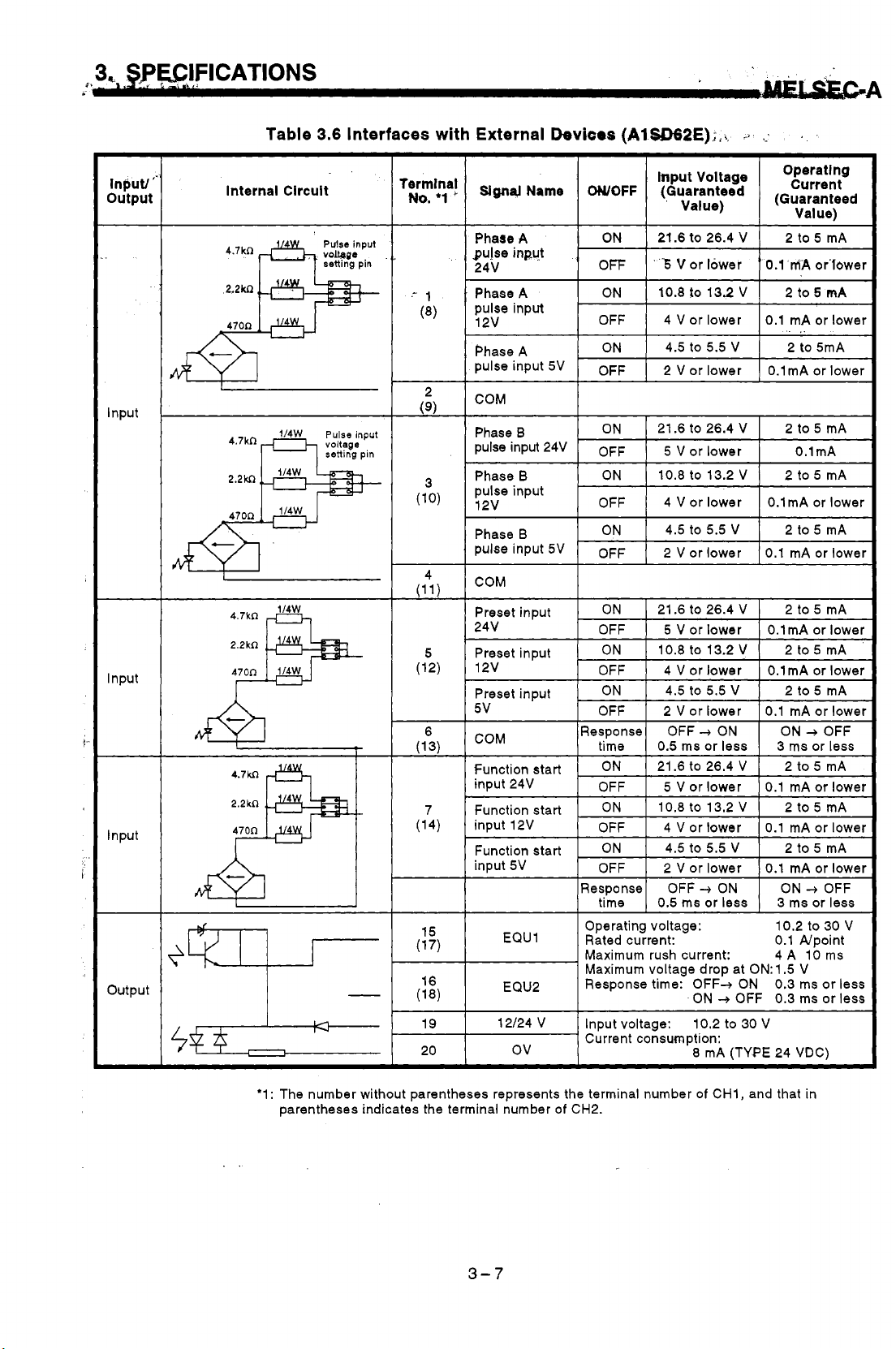
Table
3.6
Interfaces with External
Devicos
(AlSD62E);,i,
-,.
,:
.
input/
output
Input
Input
I-'
1
internal Circuit
4.7kn
4.7kR
2.2kR
fi
setting pin
put
setting pin
I
.-
1
(8) pulse input
(9)
I
11)
5
12) 12v
Signel
Name
Phase
A
puke input
24V
Phase A
12v OFF 4
Phase A
pulse input
COM
Phase
B
pulse input 24V
Phase
B
pulse input
12v OFF
B
Phase
pulse input
COM
Preset input
24V OFF 5
Preset input
Preset input
5v
5v
5v
WOFF
ON 21.6
OFF
ON
ON
OFF
ON
OFF
ON
ON
OFF 2 V or lower
ON
-
ON
OFF
ON
OFF 2
hput Voltage og:;;i:g
"'5
10.8
21.6 to 26.4 V 2
10.8 to 13.2
21.6 to 26.4 V 2 to 5 mA
10.8
(Guaranteed
Value) (Guaranteed
to
26.4 V 2 to 5 mA
V
or lower
to
13.2
V
V
or lower 0.1 mA or lower
4.5 to 5.5
2
V
5 v or lower O.lmA
4 V or lower O.lmA or lower
4.5 to 5.5
V
4
V
4.5
V
v
or lower O.lmA or lower
V
v
or lower O.lmA or lower
to
13.2
V 2
or lower
to
5.5
v
or lower 0.1 mA or lower
Value)
0.1
MA
or'iower
2 to
5
mA
-
..
2
to
5mA
to
5
mA
2 to 5 mA
2to5mA
0.1
mA or lower
to
5 mA
O.lmA or lower
2to5mA
i
output
1
f
Function start
Rated current: 0.1 Npoint
Maximum rush current: 4A 10ms
16
(18)
19 12/24
20
'1
:
The number without parentheses represents the terminal number
parentheses indicates the terminal number
EQU2 Response timer OFF4
ov
Maximum voltage drop at
V
Input voltage: 10.2
Current consumption:
of
CH2.
3-7
ON:
1.5 V
ON
OFF
30 V
0.3
0.3
ON
+
to
8
mA (TYPE 24 VDC)
of
CHI, and that in
ms
or less
ms or less
Page 20
3.
SPECIFICATIONS
I.
n
AgELSC-A
Input/
output
Input
Table
Internal Circuit
converter)
converter)
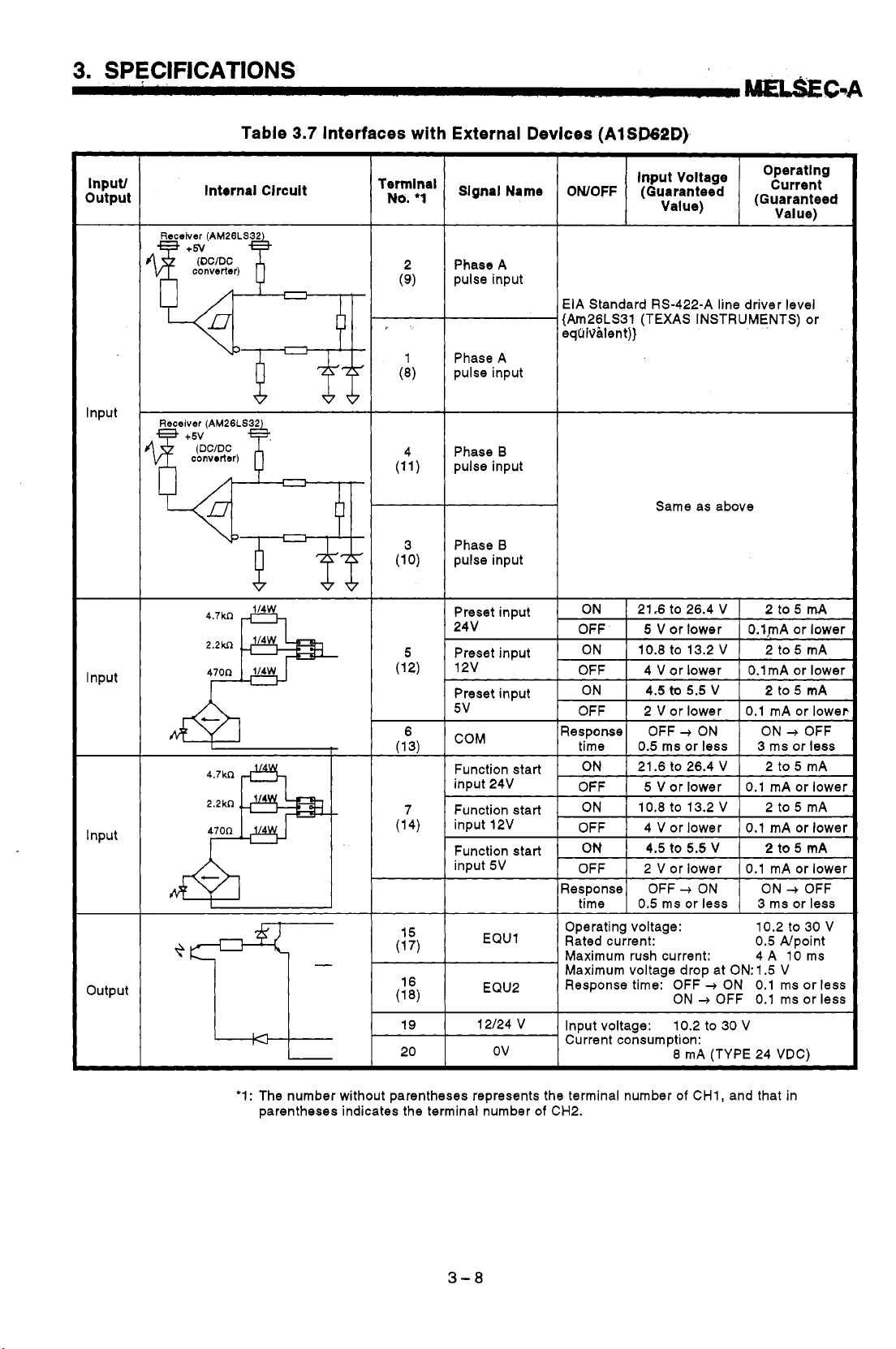
3.7
Interfaces with External
TiT!yl
2 Phase
(9)
1 Phase A
(8) pulse input
4 Phase
(11) pulse input
3 Phase
(10) pulse input
Signal
pulse input
Devices
Name
A
B
B
(AlSWPD)
Input Voltage Operating
OWOFF
EIA Standard RS-422-A line driver level
{Arn26LS31 (TEXAS
eqlriv$lent))
(Guaranteed Value)
INSTRUMENTS)
Same as above
,G~~~~~:efed
Value)
or
Input
Input
output
2.2kfl
I
w
Preset input
24V
Preset input
I
I
I
L
I
Preset input
I5v OFF
1
(1 3) time
7
(14) input 12V OFF 4 V or lower 0.1 mA or lowel
15 EQUl Operating voltage:
(1
16
(1
19
20
COM
Function start
input 24V OFF 5
Function start
Function start
input 5V OFF 2 V or lower 0.1 mA or lowel
7)
8)
ON
I
OFF
ON
OFF
ON
Response
ON
ON
,
ON
Response OFF
time
Rated current:
Maximum rush current: 4A 10ms
Maximum voltage drop at
EQU2 Response time: OFF
12/24
v
Input voltage: 10.2
ov
Current consumption:
21Sto26.4V
I
5
V
or lower I O.l,mA or lower
I
10.8
to
I
4 V or lower
I
4.5
to
I
2 V or lower 10.1 mA or lowel
OFF
+
0.5
ms
21.6
to
V
or lower 0.1
10.8
to
4.5
to
--t
0.5
ms
ON + OFF 0.1
8
I
2
to5
13.2
V
1
2
to5
I
O.lmA or lower
5.5
V
I
2
to
5
ON
or less 3
26.4
13.2
5.5
v
ON ON
or
less 3
+
to
mA (TYPE 24 VDC)
V
V
ON:
ON
30 V
ON
+
ms
or
2
to
5
mA
or lowel
2
to
5
2to5mA
--t
ms
or less
to
10.2
0.5
Npoint
1.5 V
0.1
ms
ms
rnA
mA
mA
OFF
less
mA
mA
OFF
30
V
or less
or less
'1: The number without parentheses represents the terminal number
parentheses indicates the terminal number
of
CH2.
3-8
of
CH1, and that in
Page 21
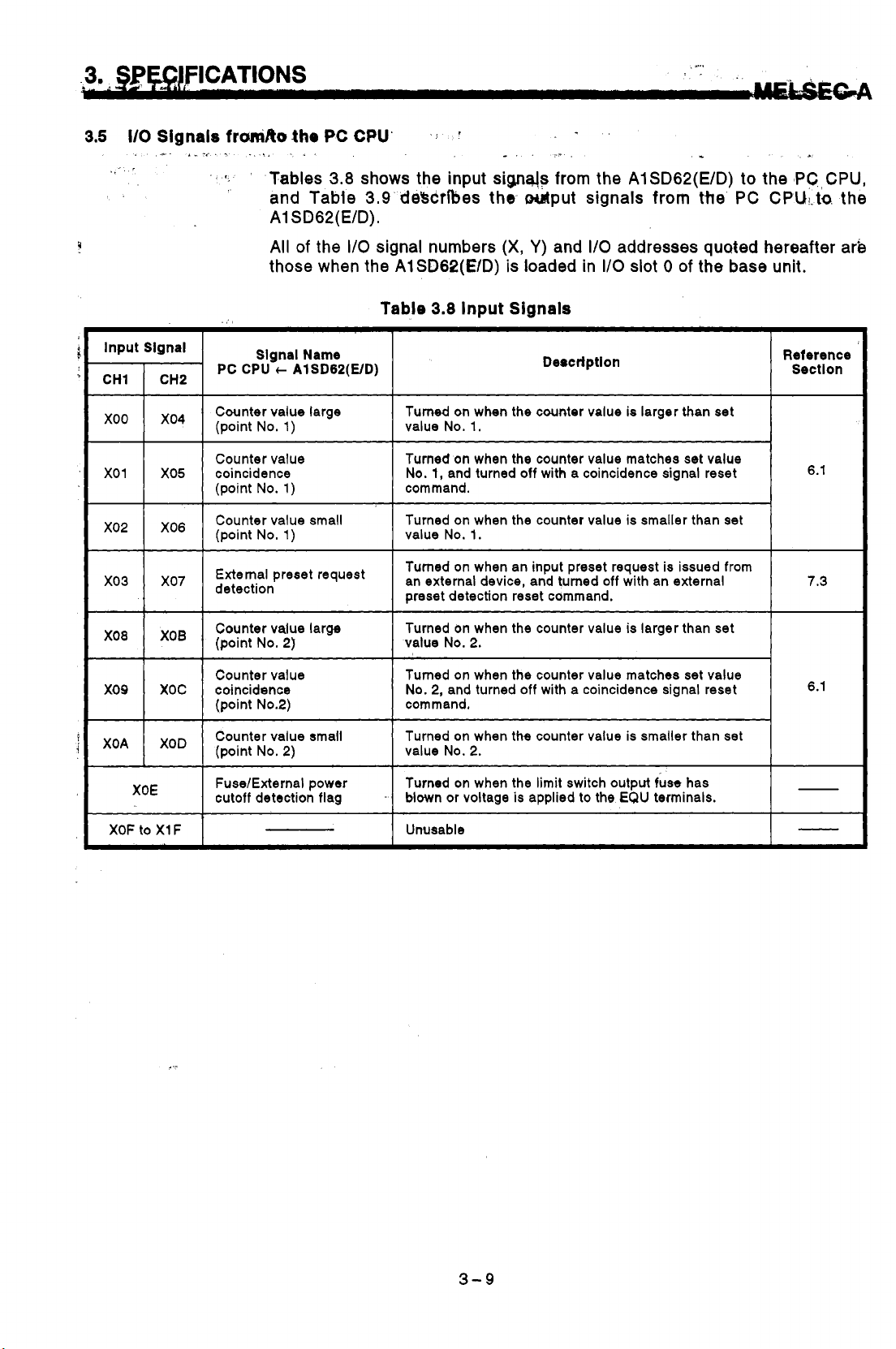
3.5
3
I/O
.
.I
Signals
.
P
'..<.
frumAo
,
'G
the
PC
.
.,,
. . .
'
Tables
and Table
CPU'
3.8
shows the input
3.9
deSCrlbes
AlSD62(E/D).
All
of
the
I/O
signal numbers
those when the AlSD62(E/D)
'
.
signals
..
.
.:
.
from the AlSD62(E/D)
the &put signals from
(X,
Y)
and
I/O
is
loaded
in
I/O
to
the
'PC, CPU,
We
PC CPL4i.h
the
addresses quated hereafter arb
slot
0
of the base unit.
Input Signal
-1
xoo
X01
xo2
X03
I
X08
XOA
1
xo4
xo6
1
X07
X0
B
XOD
Signal Name
PC CPU
(point
coincidence X05
(point
Counter value small
(point No.
I
detection
Counter value large
(point
Counter value
coincidence
(point
(point
c
AlSDIP(E/D)
No.
1)
No.
1)
1)
preset
No.
2)
No.2)
No.
2)
request
Table
3.8
Input
Signals
Dercrlptlon
Turned on when the counter value is larger than set Counter value large
value
No.
1.
Turned on when the counter value matches set value Counter value
No.
1, and turned off with a coincidence signal reset
command.
Turned on when the counter value is smaller than set
value
No.
1.
Turned on when an input preset request is issued from
an external device, and turned off with an external
preset detection reset command.
Turned
value
Turned on when the counter value matches
command,
Turned on when the counter value is smaller than set Counter value small
value
on
when the counter value is larger than set
No.
2.
No.
2,
and turned off with a coincidence signal reset
No.
2.
set
value
Reference
Section
6.1
1
6.1
XOE
XOF to
X1
FuseIExternal power
cutoff detection flag
F
Turned on when the limit switch output
blown or voltage is applied to the
-
Unusable
EQU
{use
has
terminals.
3-9
Page 22
3.
SPECIFICATIONS
-
_.
MWGA
Input Signal
YOOtoYOF
Y10
1
Y17
Y11
Y13
1
Y1A
Y14
I
Y1
B
1
Y15
Y16
Y1E
Y1F
Y1 C
1
Y1D
1
- -
I
-
Slgnal
PC CPU
t
AlSD62
Nuno
(EID)
I
Coincidence signal reset
1
command
Preset command Y18
Coincidence signal
enable command
1
Down count command
I
Count enable command
1
Count value read request memory at the leading edge
Table
3.9
Op.rcrMng
1
Timing
n
1
fl
Output
Signals
1
The signal
No.
output
device.
The signal
As soon as this signal is turned on, a
counter value coincidence signal is
issued to the external device.
Coqntdown is performed while this signal
remains
Counting is enabled when this signal is
1
ON.
The count value is written
Description
to
reset
1 signal to'the external
to
ON
tb
write a preset value.
in
single-phase mode.
~~
coincidence
to
~ ~~
the buffer
of
this
Reference
Section
I-
I
7.2.1
1-
l-
Counter function 9.2, 9.3,
1
selection start command 9.4, 9.5
I
I
1
n/n
I
I-
1
Executes counter function selection.
I
Unusable
1
Unusable
I
1
I
6.1
(1)
The operating timing shown in Table 3.9 is as follows:
n
J-l-
Valid while the signal is
Valid at the leading edge
3-
10
ON.
of
the signal.
Page 23
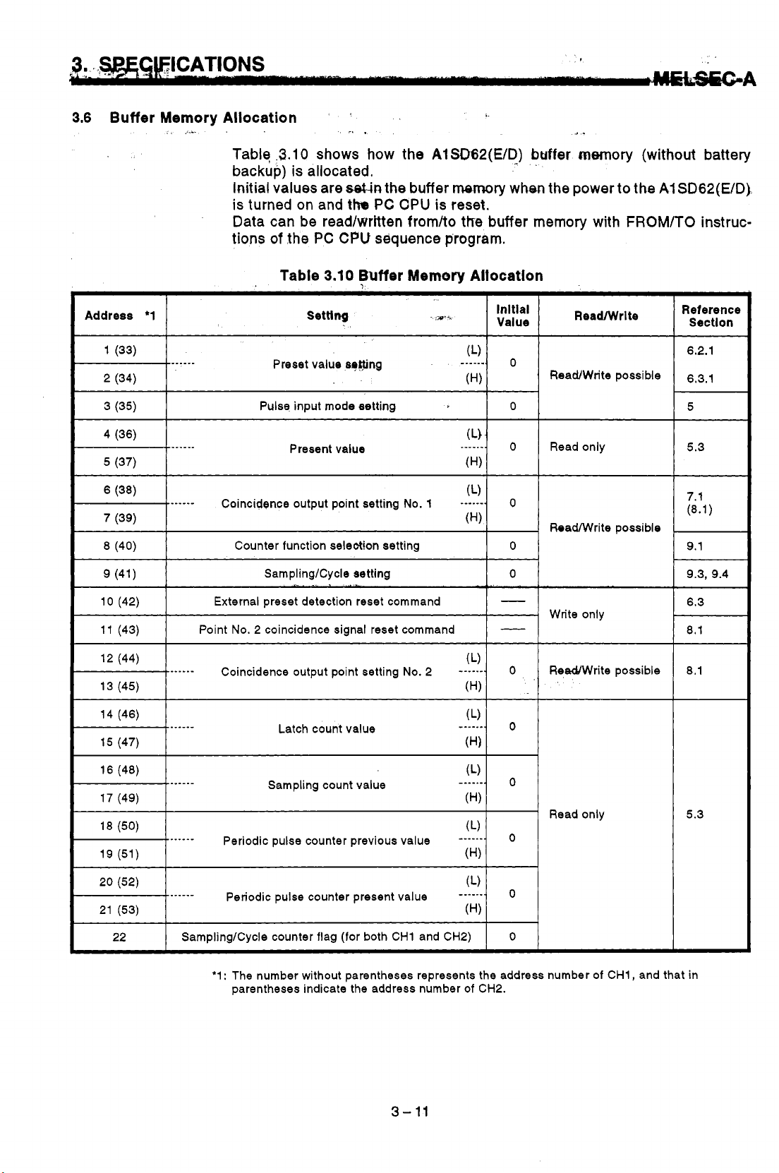
3.6
Buffer
Memory
,
,
Allocation
'
'
i.
.
+.
Address
~ ~~~~~~~ ~~
6 (38)
7
(39)
8
(40) Counter function seleotion setting
*1
- - - - - -
Table
3.10
shows how the
backup) is allocated.
Initial values are
is turned on and
setin
the
Data can be read/wrttten fromAo
tions
of
lhe
PC
CPW
Table
-
Coincidence output point setting
3.10
Setting
Buffer
.,
AlSD62(E/D)
the
buffer
m8mory
PC
CPU
is reset.
the
buffer memory with
sequence program.
Memorv
No.
1
Allocation
(
L)
------.
(HI
buffer
-.
whsn
the
~ ~~~~~~
0
ReaWrite possible
0
memory
(without battery
power to the
FROM/TO
AI
SD62(E/D).
instruc-
7.1
(8.1)
9.1
9 (41) Sampling/Cycle setting
10 (42) External preset detection reset command
No.
11 (43) Point
12 (44)
14 (46)
15 (47) (HI
16 (48)
17 (49)
18 (50)
19 (51)
20 (52)
21 (53) (HI
22
______
______-
._
- - - -
-
~-
-.
- -
- -
~-__----
Sampling/Cycle counter flag (for both CH1 and CH2)
~~
2 coincidence signal reset command
(
Coincidence output point setting No.
Latch count value
Sampling count value
2
L)
------.
(HI
(
L)
--_-_-.
(
L)
____._.
(HI
(
Periodic pulse counter previous value
L)
----.--
(H)
(L)
Periodic pulse counter present value
'1 : The number without parentheses represents the address number of CH1, and that in
parentheses indicate the address number
of
CH2.
-
-
0
Write
only
0
Read/Write possible 8.1
0
0
Read only
0
0
9.3, 9.4
6.3
8.1
5.3
3-
11
Page 24
3-.
SPECIFiCATlONS
VGA
3.7
Applicable
Encoders
.
.'
The encoders applicabte
(1)
Encoders connectable
(a) Open-collector type
(b) CMOS output type
(Make sure
A1
SD62(E) specifications.)
(2) Encoder connectable
(a) Line drive output type encoder
(Confirm whether the encoder output voltage meets the AiSD62D
specifications.)
I
POINT
7
I
The following types of encoders cannot be used with the AISD62(E/D):
TTL output type
to
the AlSD62(E/D) are shown below:
to
the AISD62(E)
that
the output voltage of the encoder complies with the
to
the
AlSD62
I
I
3-12
Page 25
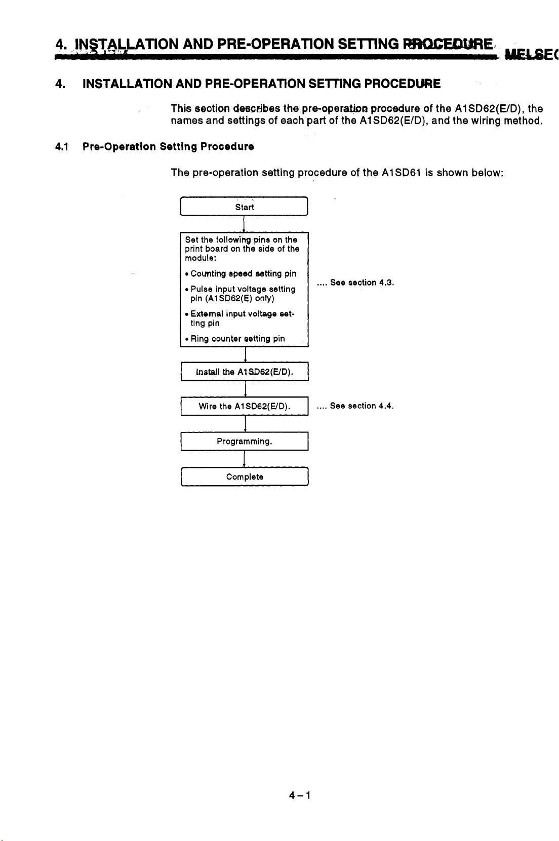
4.
.
.',
IN@TA.LAATION . AND PRE-OPERATION SEmNG
4.
INSTALLATION AND PRE-OPERATION SElllNG PROCEDURE
WC-A
This section
names and settings
4.1 Pre-Operation Setting Procedure
The pre-operation setting procedure
Set the
print board on the side
module:
e
Counting
Pulse input voltage setting
pin (A1 SD62(E) only)
External
ting pin
e
Ring counter setting pin
Install
deecdbes
,.
Start
followi'hg
aped
input
the
AlSD62(E/D).
I
pins on
setting pin
voltage
the pre-operation procedure
of
each part
of
the AlSD62(E/D), and the wiring method.
of
the AlSD61
3
the
of
the
....
See
section
4.3.
set-
of
the AlSD62(E/D), the
is
shown below:
Wire the AlSD62(E/D).
1
Programming.
1
Complete
1
1
..#.
See
section
4.4.
4-1
Page 26
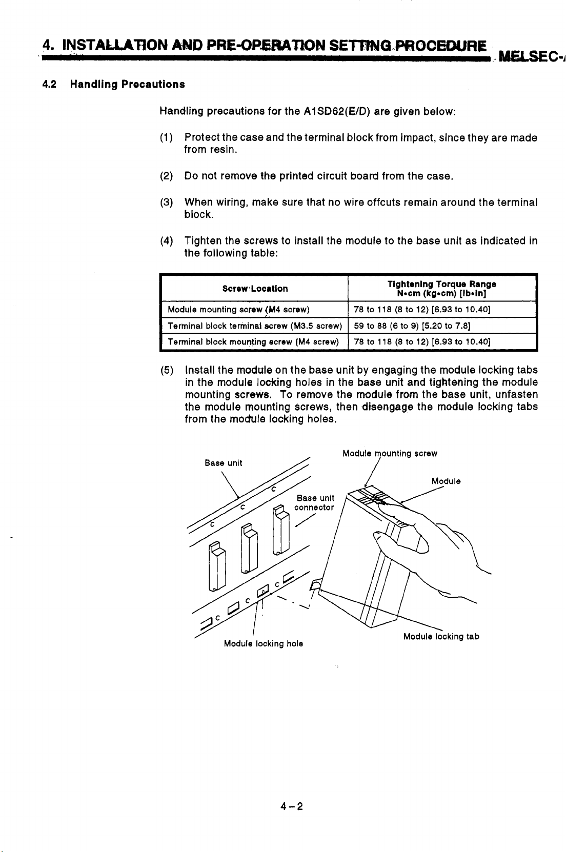
4.2
Handling Precautions
Handling precautions for the
(1)
Protect the case and the terminal block from impact, since they are made
from resin.
(2)
Do
not remove the printed circuit board from the case.
(3)
When wiring, make sure that no wire offcuts remain around the terminal
block.
(4)
Tighten the screws
the following table:
I
I
Module mounting screw
Terminal block terminal screw
I
I
Terminal block mounting screw
(5)
Install the module on the base unit by engaging the module locking tabs
in the module locking holes in the base unit and tightening the module
mounting screws.
the module mounting screws, then disengage the module locking tabs
from the module locking holes.
Screw, Looation
(M4
AISD62(E/D)
to
install the module
screw)
(M3.5
screw) I 59 to
(M4
screw)
To
remove the module from the base unit, unfasten
are given below:
to
the base unit as indicated in
I
I
78
I
78
Tlghtenlng
Nacm (kgocm) [Ibmln]
to
118
(8
88
(6
to
118
(8
to
to
to
12)
9)
12)
Torque
[6.93 to
[5.20
t6.93
to
7.81
to
Range
10.401
10.401
I
I
I
I
Base unit
Module locking hole
Module mounting screw
/
4-2
Page 27
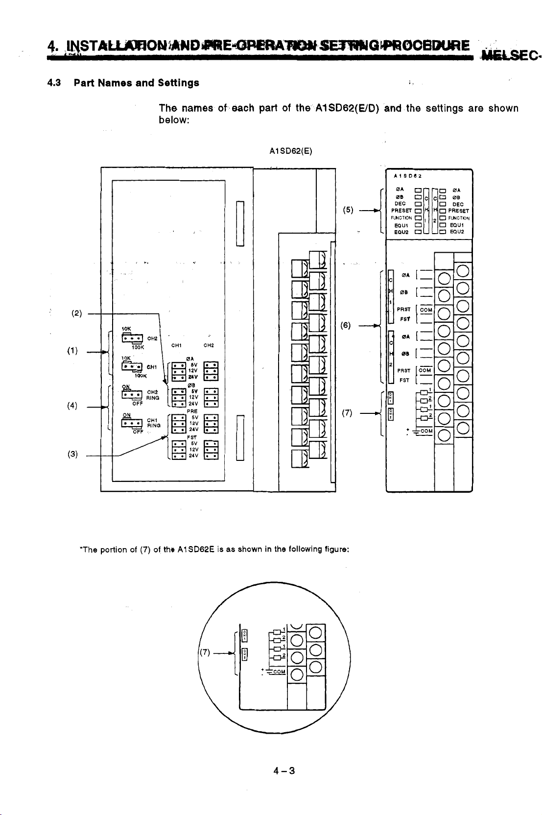
The
names
below:
of..each
part
of
A1 SD62(E)
the
AlSD62(E/O)
and
the settings are shown
r
1
I
,-
0A
C
H
08
1
..
PRST
$St
<-
CH2
CHl CH2
OK
1
lPOK
08
04
BB
PRST
FST
.I
(4)
-
'The portion
of
(7)
of
the
,
.
24v
AlSD62E
is
as
shown in
the
following figure:
+
4-3
Page 28
4.
INSTALLATION
-
No.
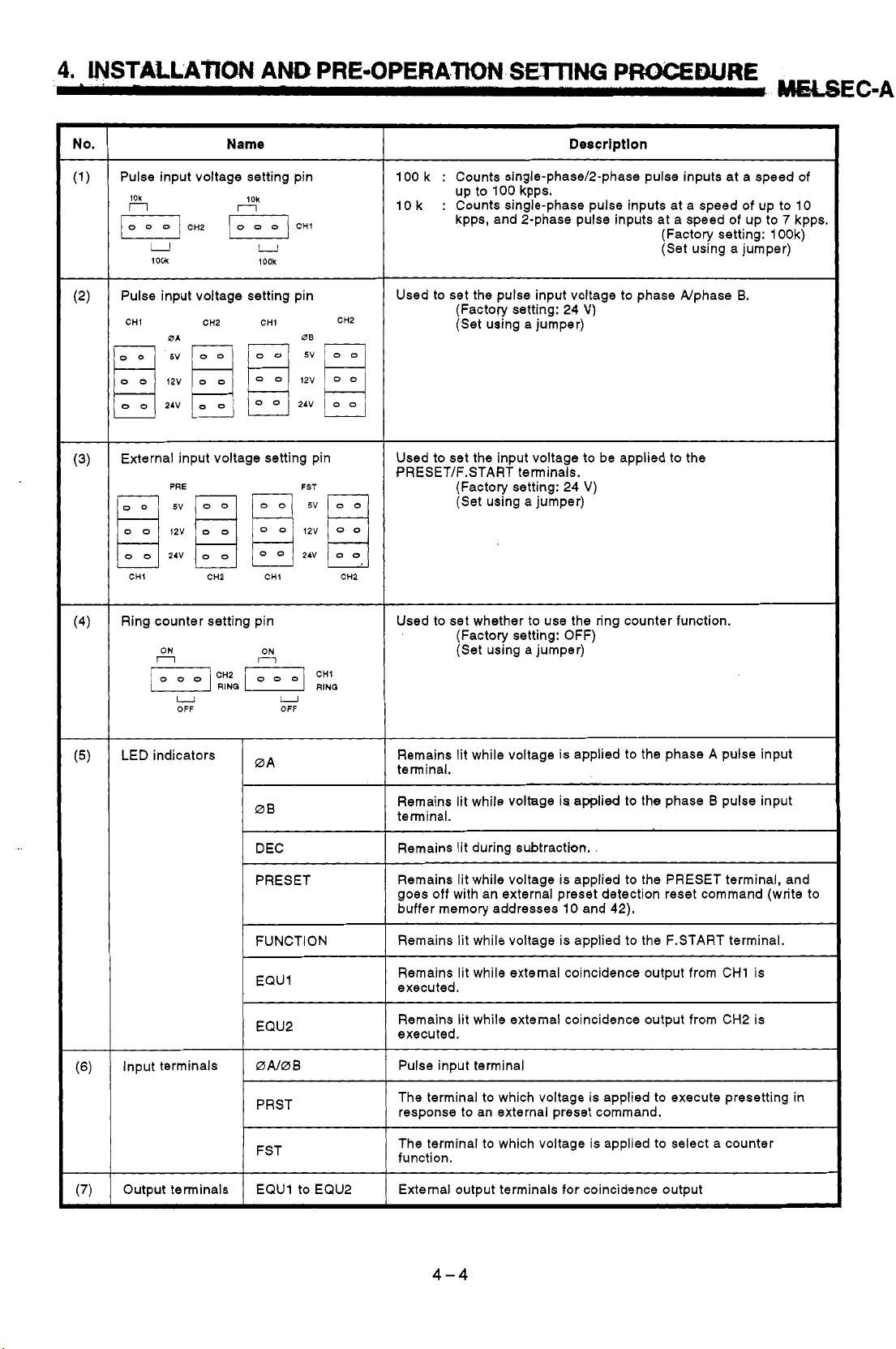
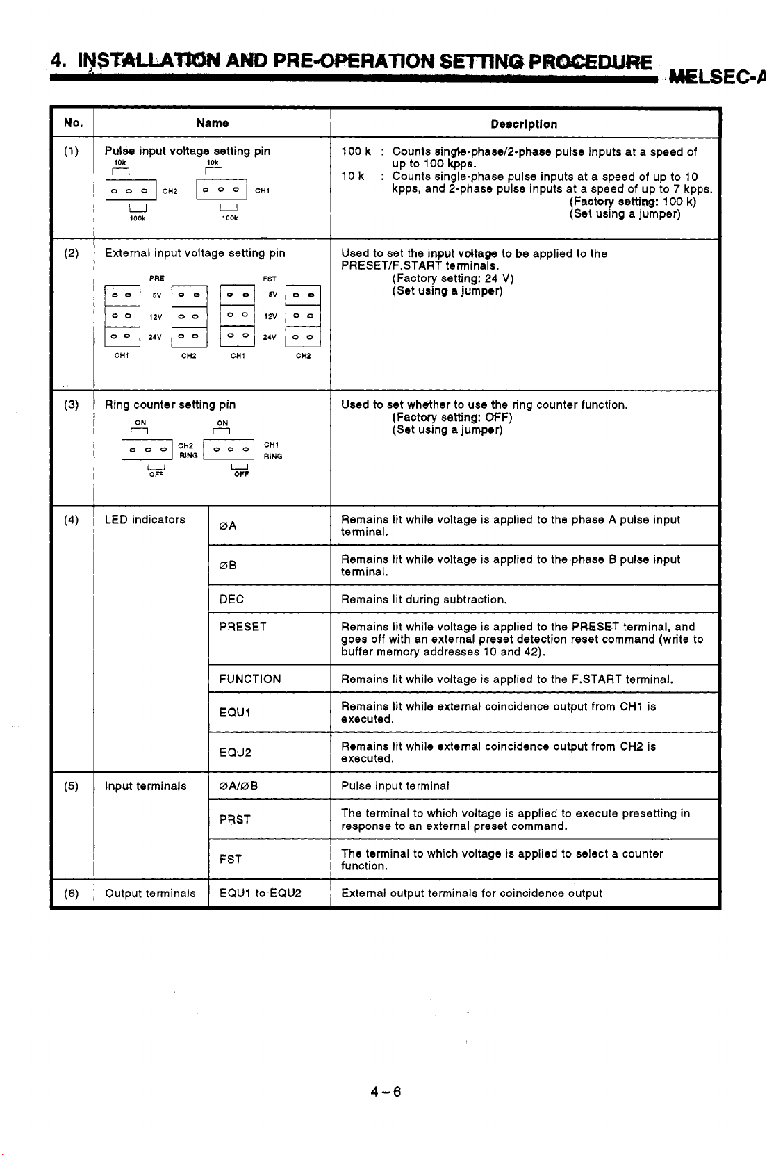
Pulse input voltage setting pin
1Ok
n
/ooo/
Pulse input voltage setting pin
CHl CH2 CH1 CH2
U
lorn
CH2
10k
n
F]
AND
-
CHI
U
100k
PRE-OPERAlnON
100
k : Counts single-phase/2-phase pulse inputs at a speed of
up
to
10
k
Used
:
to
100
Counts single-phase pulse inputs at a speed of up
kpps, and 2-phase pulse inputs at a speed of up
set
the pulse input voltage
(Factory setting:
(Set using a jumper)
SETTING
Description
kpps.
24
V)
PROCE
(Factory setting:
(Set using a jumper)
to
phase Nphase
WRE
~ ~ ~ ~~~~~~
B.
1
MELSEC-A
to
10
to
7
kpps.
1
OOk)
0A
0B
,tH
24V
U
OFF
g:R
0
0
24v
External input voltage setting pin
Fqqq
0
0
24v 24V
CH1 CH2 CHI CH2
Ring counter setting pin
U
OFF
LED
indicators
i-1
0
m::fl
Used
to
set
PRESET/F.START terminals.
0
0
Used
Remains lit while voltage is applied
terminal.
Remains lit while voltage ia applied
terminal.
the input voltage
(Factory setting: 24
(Set using a jumper)
to
set whether
(Factory setting: OFF)
(Set
to
using a jumper)
to
be applied
V)
use the ring counter function.
to
the
to
the phase A pulse input
to
the phase B pulse input
Input terminals
Output terminals
DEC
PRESET
FUNCTION
EQUl
EQU2
%N0B Pulse input terminal
PRST
FST
EQUl to EQU2
Remains lit during subtraction.
Remains lit while voltage is applied
goes off with an external preset detection reset command (write
buffer memory addresses 10 and 42).
Remains lit while voltage is applied
Remains lit while external coincidence output from
executed.
Remains lit while external coincidence output from CH2 is
executed.
The terminal
response
The terminal
function.
External output terminals for coincidence output
to
which voltage is applied
to
an external preset command.
to
which voltage is applied
4-4
to
the PRESET terminal, and
to
the F.START terminal.
CHI
is
to
execute presetting in
to
select a counter
to
Page 29
A1
SD62D
&I
200K
f2
'
200K
CH2
CHI
T
7
I
A'SD62D
PRST
F
PRST
F
I
0A
OB
ST
0A
00
ST
4-5
Page 30
No.
Name
~~
Description
Pulse input vottage setting pin
1Ok 1Ok
n
(beol
External input voltage setting pin
Ring counter setting pin
(4)
I
LED
CH2
U
look look
ON
n n
indicators
r-
Fl
CH1
U
CH1 cn2
ON
0A
100
k
:
Counts singte-phase/2-phase pulse inputs at a speed of
up
to
100
:
10 k
Used to set the input
PRESET/F.START terminals.
Used
Remains lit while voltage is applied to the phase A pulse input
terminal.
Counts single-phase pulse inputs at a speed of up to 10
kpps, and 2-phase pulse inputs at a speed of up to 7 kpps.
(Factory setting: 24
(Set using a jumper)
to
set
(Factory setting: OFF)
(Set
kpps.
voltage
whe4her
to
use
using a jumper)
(Factory
(Set using a jumper)
to
be
applied to the
V)
the ring counter function.
settiw:
100
k)
(6)
I
Input terminals
Output terminals
0B
DEC
PRESET
FUNCTION
EQU
1
EQU2
0N0B Pulse input terminal
PBST
FST
EQUl to
EQU2
Remains lit while voltage is applied to the phase
terminal.
Remains lit during subtraction.
Remains lit while voltage is applied to the PRESET terminal, and
goes off with an external preset detection reset command (write to
buffer memory addresses 10 and 42).
Remains lit while voltage is applied to the F.START terminal.
Remains lit while external coincidence output from CH1 is
executed.
Remains lit while external coincidence output from CH2 is
executed.
The terminal to which voltage is applied to execute presetting in
response to an external preset command.
The terminal to which voltage is applied to select a counter
function.
External output terminals for coincidence output
B
pulse input
4-6
Page 31

4.4
wring
4.4.1
..
Wing
Details
described below:
preconditions
The preconditions when a pulse generator device
are described
(1) For a high-speed pulse input, take the following counter measures against
(2) For 1-phase input, connect count input signal
(3)
(4)
on
how
-to
wire a pulse generator device
to
is
wired
the
AlSB62(UD)
to
the A1 SD62(E/D)
are
below:
noise:
(a) Be sure
grounded
Do
(b)
not run a twisted pair cable in parallel with power cables or other
I/O
lines which
(5.91
in.)
use shielded twisted pair cables.
to
Class 3 specifications.
may
generate noise. Run cables at least
away
from the above-mentioned lines and over the shortest
Also,
make sure it is
150
mm
to
distance possible.
to
phase A only.
If
the AlSD62(E/D) picks
up
pulse noise, it will count incorrectly.
The specific measures against noise are shown below:
A1
PC
arate
more
from
[Also
taka
thgn
equlp-
cere
It8
mrn
meni such as Invert-
ern.
of
wiring inside the
panel.)
Y
A
Ground twisted shielded wire on the encoder side (joint box). (This is a connection example for 24 V sink loading.)
I
I
/
SD62(E/D)
Metal piping. Never run solenoid or inductive wiring through the same conduit.
If
sufficient distance cannot be provided between the high current line and input
wiring, use shielded wire for the high current line.
Encoder
Joint
Distance between the encoder and the joint
box should be as short as ossible.
tance from
box
too long, anrxcessive voltage drop occurs.
Therefore, measure
tion and make sure that the voltages are
within the rated voltage
voltage drop is large, increase the size of wir-
ing
rent consumption.
the
A1
SD62(E/p) to the encoder
the
er
use
an encoder of 24 VDC with
voltage during opera-
of
the encoder.
If
the dis-
less
If
IS
the
cur-
to
Connect the encoder shield wire
shield wire of the encoder that is not grounded In the
encoder. Ground it inside the joint box as indicated by
dotted line.
I
I
the twisted pair
4-7
Page 32

4.
INSTALLATION
AND
PRE-OPERATIOH
SEmNG
.PROCEDm
.:
:
XISEC-A
4.4.2
Wiring
A1
SD62(E)
example
for
the connection with the open collector
(1)
Connection
of
a
24
VDC
pulse generator
output
pulse
generator
Pulse generator
The encoder signal and
A1
SD62(E) CORRECT:
?==)I
INCORRECT:
supply
lines should be
wired
as shown below:
Since the same twisted pair wire is
used for both the encoder signal and
the power supply, a reduction in the
canceling effect and electromagnetic
Induction may occur.
4-8
Page 33

A1
SD62(E)
1)
Set the pulse input voltage setting pin
(2)
Connection
of
a voltage
to
We
output
Twisted pair wire
wise generator
h
.'
position.
(5
EC-A
VDC)
Pulse generator
r
---.-.-
IREMARK]
1)
Set
the pulse input
voltage
setting pin
to
the
m
position.
,
4-9
Page 34

A1
SD62D
(3):
Wirlng exampie between the
driver (Am26LS31
or
equivalent)
AlSD62D
and a pulse
Pulse
generator
generator
for
line
....
J
4- 10
Page 35

EC-A
4.4.3
YU~~~mple
F.START)
A1 SD62(E/D)
This diagram assumes that
AlSD62(E/D)
for
the
mnnectkm
(1)
When a controller
External input voltage
setting pin
the
intemat circuit is set to PRESET.
(2)
When
of a
riaaWkr
(sink
acentroller (source load type)
SET
or
F.START
bexbmqtinput
load type) is supplied with
is
supplied
terminals
12
Controller
with 5 V:
Controller
.-.-.-.
(PRESET
V:
VDC
and
-I
1
This diagram assumes that the internal circuit is
IRE MARK^
(1) Set the pulse input voltage setting pin to the
set
to
PRESET.
m
1
position.
4-
11
Page 36

4.
INSTALLATION
,.
.
ANU,F4MXW€RATtON
SETTUW
pwacEouRE
.
I
MELEC-A
4.4.4
Wiring
examples
To
For this example, 10.2
methods are as follows:
(1)
at
external output
termids
use an external terminal,
to
AlSD62(D)
(Mus
30
1
to
2)
the
internal photocoupler should be activated.
VDC external power is necessary. Connection
-
+
10.2V
to
30V
(2) A1 SD62E
...
+
10.2V
to
30V
4-
32
Page 37

.
. .
This section describes the pulse
AISDM(E/D).
(1)
The pulse input mode is classified into single-phase pulse input and
'
'
2-phase pulse input. Single-phasepcllse input
plication by one and multiplication
input
8nd counting modes of the
I
is
subdivided into multi-
by
two, whereas 2-phase pulse input
covers multiplication by one, two and four.
Table
5.1
shows the pulse input modes and the count timing.
Puke Input
Single-phase,
multiplied by one
Single-phase,
multiplied by two
2-phase,
multiplied by one
Mode
Table
5.1
I
In up count
In down count
I
In
upcount
In down count
In
up count
In down count
Pulse
1
/0B
IDA
Input and Count
Count Timlng
.BA
JlJL
0B
Y13
(Y1 A)
@A
OB
Y13
J-L
(Y1A)
0A
0B
(Y1 A)
0A
_f-Lf-L
0A
TlTl
m
m
Timing
Counts a pulse at
0A.Yl3 (YlA)
Counts a pulse at 1 of
0A.Yl3 (YlA)
Counts a pulse at t and
1
of
0A.Yl3 (YlA)
OFF.
Counts a pulse at f and
1
of
0A.Yl3 (YlA)
ON.
Counts a pulse at
0A.
The pulse count
increases in response
to
the phase difference
between
Counts a puke at
0A.
The pulse count
decreases in response
to
the phase difference
between
OA
OA
are
are
and
and
0B.
0B.
t
of
OFF.
ON.
are
are
t
of
.1
of
2-phase,
multiplied by two
In up count
In down count
.5
-
I
0A
0B
m
m
Counts a pulse at 7 and
1
of
0A.
The pulse count
increases in response
to
the phase difference
0A
and
in
response
and
0B.
0B.
between
Counts a pulse at t and
1
of
0A.
The pulse count
decreases
to
the phase difference
between
0A
Page 38

Pulse Input
Mode
I
Count Timing
.
2-phase,
multiplied by four
(2)
Even
value at
up
count
In
In down count
if
the
pulse
the
time the.mode is changed.
input mode
is
changed, counting
Counts a pulse at
L
of
0A
The pulse count
increases in response
to
between
Counts a pulse at T and
5.
The pulse count
decreases in response
to
between
and
the phase difference
0A
of
0A
and
the phase difference
0A
will
start from the
0%.
and
OB.
and
T
and
0B.
0B.
5-2
Page 39

5.1
SingieWiase
Pufsi
Input
I'
,.
,.
.,
'!
In single-phase pulse input, multiplication by
counting.
(1)
The
,,
-
following figure
and a down count command.
Encoder
/
(2)
Counting mode setting
To
use this counting mode,
memory (address
shows
Down'count command
0
{or Y13 (YlA)
3
(35))
the relationship between phase A pulse input
Pulse
of
gram.
Counting Mode Set Value
one
oqtwo can be selected for
Ai SD62(
UD)
R
.
,
input
ON}
set
the
the
AlSD62(E/D) using the sequence pro-
>*,
0A
@B
pulse input mode setting buffer
Multiplication by one
Multiplication by two
[Sequence program]
Write
command
IREMARKS
(1) In
[
the A1 SD62(UD).
(2) Set 3 in
(3) In
S,
I[
1,
set the first
[ ]
set
KO
I
two
for CH1,
or
representing multiplication by one, or
digits
of
the hexadecimal three-digit first
35 for CH2.
110
number allocated to
K8
for multiplication by two.
5
-3
Page 40

5.2 Counting at 2-Phase Pulse Input
When the 2-phase:pufse
from multiplication
(1)
The relationship between the phase A pulse input and the phase B pulse
input
is
Encoder
(2)
Counter processing mode setting
To
use the above-mentioned mode (counting using the incremental
phase
A,lS@2(E/D)
to
A
any number from 2
by
given below:
pulse input and decrementat phase
pulse input mcde setting bdfer memory {address
inpld
one,
two,-and four.
Phase A
to
Counting
is
done,
4
using the sequence program.
hode
the counting mode can be selected
A1
SD62(E/D)
1
J
getting
B
pulse input),
Value
set
the
3(35))
I
I
[Sequence program]
Write
command
[
I[
1,
1) In
the A1
2)
3)
set the first two digits
SD62(UD).
Set
3
in [ ] for CH1, or
In
S,
set
K2
representing multiplication by one, K10 for multiplication by two, or K18
multiplication by four.
Multiplied by
Multiplied by
Multiplied by four
35
for CH2.
one
two
of
K2
I
'I
the hexadecimal three-digit first
K10
K18
I
I
I/O
number allocated to
for
5-4
Page 41

5.3
Reading the Present Value
L.
.
This
section givea.details
present value
to
read it.
(1)
The buffer memory
@torage
on,#hq?rrsant
buffer;memory
stores
the
value
(addrewes
cwnt
value
stored in the
4
to
5
(36
when the following are in
,
'*
AlSD62(E/D)'s
to
37)},
and how
effect: pulse input, presetting, ring counter function execution or count
disable (counter function selection).
However,
periodic pulse
count value when the latch counter, sampling counter
counter
function is executed
will
be stored in the counter
or
the
function selection count value storage buffer memory shown in Table
5.3.
Table
5.3
Counter Function Selection Count
Value Storage Buffer Memory
Perlodlc Periodlc
Previous
to
50
to
51
24-bit
Descrlptlon
Buffer
memory
bdctt'ess
I
(2)
The present value
CH1
CH2
14to15
46
(0
to
Latch
Count
Vdue
to
47
16777215)
Count
Value
to
48,to
is stored in
17
49
present value storage buffer memory.
(3)
In up count, the present value storage buffer memory returns
the count value reaches
1677721
In down count, the buffer memory returns to
value reaches
0.
5.
1677721 5
Pulse Count Pulse Count
Present
Value Value
19 16
20
52
binary in the
to 0 when
when the count
to
to
21 18
53
5-5
Page 42

5.
PULSE
INPUT
AND
(4)
Shown
in
cO.l,WTEU
below
the
present value
Is
Pt!SOCBS~M€~D
the
sequence
storage
program
to
read
buffer memory.
the
present value stored
(a) Reading using FROM/TO instructions (when
PC
selected as the
Read
,
command
Set
data
n
A1
SD62(VD)'s
Firot
*
D
1)
Set
2)
The present value
AlSD62(E/D)
.I
.*
1
device numbrr.to
a count value read request Y(n + 15).
CPU I/O control method)
DFRO
I
first
I/O
number
store
is
set
for n, and is stored in the device
fram.wh1d.l
I
.;..
*.=Pi..
the
repd
read from
the
-.
.
.
present
the
I/O
present value
value
number of the
In present value reading, data is read directly from
AlSD62(E/D)'s buffer
CH1)-or
No.
36 and
No.
rnerrhry
37 (for
addresses
CH2).
the
SET
n
I
K4(K36) 1 D
No.
direct method is
I
Y
(ntl5)
I
K1
will
be
read
set
for D.
4
and
No.
5
I
(for
3)
Reset
the count value read request Y(n + 15).
5-6
Page 43

..
'
14
(b)
Reading:
using.PRobdiT-0
sebcfed'asJW~PCaUPF%LP
Read
instructions
(when
t'Klcbnttwtmethod)
the refresh method is
Frn
RST
I
Y
(n+15)
t.
.
.-
Set
data
n
AiSb'62(Eh)'s
-.
Cd
First device number to store
D
first
I10
number from
whichthe
the
read present value
present value
will
be read
1)
Set a count vatue read request Y(n
2)
The
presant
AlSD62(E/D) set far
In
present
A1
SD62(E/D)'s buffer memory addresses
CH1)
or
3)
Designate partial refresh.
4)
Y(n + 10)
5)
Reset the count value read request Y(n
value
No.
to
value is
wad
n,
and
from the
is
stored in the device
reading, data is read directly from
36
and
No.
37
(for
CH2).
Y(n
+
ID)
are partially refreshed.
+
15).
I/O
number of the
No.
+
15).
4
set
and
for D.
No.
5
(for
5-7
Page 44

(c)
Read
Reading
using an
A2ASCPU(SI/S30)
dedicated
instruction
LEDA
...
Reading is
executed when
the command
ON.
...
LEDB
Reading is
executed at the
leading edge
the
is
of
command.
I
LEDR
r----,
Instruction symbol in
I
L----I
I
IPVRD1,PVRD21
Set
data
n D AlSD62(WD)'s
First device number to
1) The present value is read from the I/O number of the
AlSD62(E/D) set for n, and is stored
In present value reading, data is read directly from
AlSD62(E/D)'s buffer memory addresses
CH1) or
The channel for present value reading depends on the instruc-
to
tion
2) In present value reading using a PVRD1 or PVRD2 instruction,
ON/OFF
Y(n+l C) (count value read request) is automatically executed
internally, which means that the user does not have
it.
first
No.
36 and
be used.
control
I/O
number
store,~,the
PVRD1 instruction
PVRD2 instruction
of
the AlSD62(E/D) I/O signals Y(n+l5),
from
read present value.
No.
37 (for CH2).
which
........
........
the
present value will
to
the device
No.
For CHI
For CH2
4
set
and
be
No.
to
read
for D.
5
(for
execute
POINTI
To
perform communications with a special function module using an
APASCPU(Sl/S30) dedicated instruction, register AD61 as the module
type when setting parameters.
5-8
Page 45

6.
EXECUVINQ,THfi
-6.1
Coincidence Output Function
GOtNBIDENCE
This section describes the coincidence output function.
The coincidence output function issues a signal when a preset count value is
compared with and matches the present counter value.
Two coincidence output points can be set.
To use the coincidence output function,
command to
[Example of how to use the coincidence output function]
Manufacturing products by performing each machining operation in response
to a coincidence output in a machining line system.
ON.
BUTPUT~FUWFION
set
the coincidence signal enable
(1) The material is conveyed by a belt conveyor.
,.
.
(2)..~-T:ke.material
.is determined
13)
As
soonas
machining operation takes place in response to a coincidence output
(EQU1, EQU2) from the AlSD62(E/D).
positionambe identified as4he present count value which
by
a
pulse
sent
the
material
is
located at each specified position, the relevant
Part
cutting
to
/.
the
AlSD62(E/D).
Drilling
n'
67
!
0:
T
6-1
Page 46

6.1
.I
Coincidence output function operation
Count,embk command
{Y14
(YlB)}
OFF
Coincidence signal enable
command
Input
Coincidence
setting
{addresses
Counter value small
(point
Counter value coincidence
(point
Coincidence signal reset
command
{Y12 (YlQ)}
pulse
to counter
out
No.
1
buhr
to
6
No.
1) {X02 (X06)}
No.
1) {X01 (X05)}
{YlO (Y17)}
ut
7
point
memo
(38
to
38)
OFF
Present value storage
buffer
memory
4
to
5
...
(36
The
{addresses
(1)
the
6
to
(2)
...
When the counter value reaches the
value, the counter value small stpal is turned
value coincidence signal is turned on.
(3)
...
The coincidence signal reset command is turned on, and the counter
value coincidence signal is
The subsequent coincidence signal output does not take place as
long as the counter value coincidence signa4 remains on.
(4)
...
When the counter value is larger than the
point value, the counter value large signal is turned on.
',!Ill
'
0,
1, 2,
to
37))
set
coincidence output point value is written in 24-bit binary
coinckfence
7
(38
to
output
39))
point setting
of
the
AlSD62(E/D)
to,
98, 99:100:101:102~103~
No.
1
buffer memory {addresses
in advance.
set
coincidence output point
off,
and the counter
reset.
set
coincidence output
to
6-2
Page 47

6.1.2
Program
Examples
T~e
one mode using
[System configuration]
following
program
CH1,
and ,exebute
is
to
count pulses in
X00
to
XiF
YOOtoYIF
2-phase
the
limit switch,w'put function.
X20t0x3F
pulse input multiplied by
[Devices
(1)
(2)
DO
to
be used]
Execution commands
(a) Pulse input mode setting command
(b)
Counting start command
(c) Present value read command
(d) Coincidence output data setting command
(e)
Coincidence output command
(f) Coincidence signal reset command
(9) Counting stop command
Relationship between data registers
Buffer
Address Setting
'L,
3
Pulse input mode setting
............................................
...................................................................
...........................................................
....................................
..........................................................
.................................................
........................
(DO
memory
..
...........................................
to
D4)
and the buffer memory
M9038
X20
X21
X22
X23
X24
X25
6-3
Present value
---I
I->
Dl
to
D2
Page 48

(a)
Execution using
selected
as
the
PC CPU
FROM/TO
I/O
instructions (when the direct method
control method)
(Program]
Pulse input mode setting
PK
I
PH
TO
Counting start
r-------------------------------------------------------------
Present value read
0000
{
MCV
2
K K
3
DO
[SET
YOI~+/
is
Set
2-phase pulse
input multiplied by
1
one mode.
Start ulse counting
with
tle
count enable
command.
H
DFRO 0000
__________-_____________________________---------------------,
Coincidence output data setting
P
DMOV
PH K K
[
DTO 0000
Coincidence output command
b23
K
4
[SET
[
RST
K
2000
6
Dl
<
D5
YO12
YO15
Read the resent
value, anSstore it
to
Dl
to
D2.
I
I
,
Store the set coincidence
output point value in buff-
,
er memory addresses
6
to
No.
1
The coincidence signal
can be issued
7.
external device with the
coincidence signal enable
command ON.
to
No.
the
Counting stop
CIRCUIT
END
6-4
{
RST
YO14
Stop ulse counting
4
with t e count enable
command reset.
Page 49

..
(b)
EndofYublng
sB1.e;cfed
as
PW"O
PC
CPU
WO
ine#Wions
Control
method)
(when
the
refresh method is
The portions of the program example shown in
broken and dotted lines must be replaced with the following:
Present value read
t
c
I
Coincidence .signal reset command
/;,',{SET
{SEG
L
RST
K4
YOIO
YO15
YO1
K4
EOOI
Read
and
Reset
signal.
I--
(a)
enclosed by the
the
present value,
store
It
to
Dl
the
coincidence
to
D2.
Page 50

6.
EXECUTING
<.
THE COINCIDENCE OlJTPtlT
FUMCTlON
MwsEGA
Present value read
(c) Execution using MASCPU(Sl/S30)
As shown below, A2ASCPU(Sl/S30) dedicated instructions can be
used In place
enclosed by the broken line.
of
the portion
of
I
POIrdTl
To
perform communications with a special function module using an
A2ASCPU(Sl/S30) dedicated instruction, register AD61 as the module
type when setting parameters.
dedia?ed
the program example shown in (a)
r
LEDR
instructions
Read the present value,
and store
it
to
LI
Dl
and
D2.
6-6
Page 51

The preset function is used for converting the counter's present value
<
,-
different value.
This changed value
is
called the preset value.
to
a
The preset function can be used when a pulse count is started from the set
value.
The preset function consists of two modes: preset by the sequence program
and preset from the external control signal (applying the voltage
to
the
external terminal).
Preset function application example:
By using the preset function, the production count can be continued from the
previous day.
(1)
The production volume
to
the
AlSD62(E/D).
(2)
Products are carried
(3)
The
production volume is counted by inputting the pulse from the photo-
of
the previous
by
a conveyor.
day
ip
'preset" from the PC CPU
electric switch.
(4)
At
the end of the daily production, the counter value in the buffer memory
is stored
to
a word device
(D,
W,
etc.) in the PC CPU latch range.
I
7-1
I
I
I
I
Page 52

7.-
EXECUTING
~
L.
..
THE PRESET
FWmQN
7.2 Preset Using the Sequence Program
The following describes the preset function executed by the sequence program.
7.2.1 Executing the preset function using the sequence program
Turn
ON
the preset command
(Y11
(Y18))
in the sequence program
the preset.
.
..
MELSEGA
to
execute
Count enable command {Y14 (YlB))
Input pulse to be counted
Preset value setting buffer memory
{Addresses 1 to 2 (33 to 34))
Present value
{Addresses 4
storage
to
5
(36
buffer
memory
to
37))
1)
Writes a given value
(addresses
2) Turing
the
in
buffer memory
The preset function can be used whether the count enable com-
{Yl
mand
ON
Y5
OFF
I
I
I
I
to
1
to
2
(33
to
ON
the preset command
to
4(Y
1
B))
is
ON
IIIIIII
I,,,,
IIIIIII
IIIIIII
IIIIIII
the preset value setting buffer memory
34))
in
24-bit binary code.
(Y11
(Y18))
sets the preset value
the present value buffer memory.
or
OFF.
7-2
Page 53

7.2.2
Example program
\
~
,
I
-
';*?
.,
.,
Create
the preset function using the sequence program.
System configyation:
A1 S62P D62
a
prbgm'm-tailQunI
,.*.@ii
C"
X00
rYOObYlF
A1 SCPU
,
:.
to
A1
S
WD)
2-pheee
'
..
XlF
X20
:::
pukes. multipbd by one and
to
83F
L
Devices
(1) Execution commands
to
be used:
(a) Pulse input mode setting command
.I
(b) Count operation start command
(c) Present value read command
(d) Preset value write command
.
(e)
Preset reset command
.......................................................................
...........................................................
............................................................
............................................
.......................................................
.>
to
execute
M9038
X20
X21
X22
X23
(f)
(2)
Relationship
D3 to D4
.
Count operation
between
Address
l+l--
stop
command
data register
Buffer memory
Pulse input mode setting
--
.......................................................
(DO
to
D4)
and buffer memory
Contents
Present value
Present value
_-
(HI
X24
Dl to D2
7-3
Page 54

7.
EXECUTING
THE PRESET
(a)
Execution using
wkcted
[Program]
FUWXION
FROM/TO
as
the
PC
CPU
-
, . ,
-
.
,
instructions (when
1/0
control method)
_'
,
MEIA
the
direct method
is
,
.
.
Pulse input mode setting
:c
'
Preset command
I
I
PK
[
MOV
2
PH K
[
TO
__E
I
I-[
DFRO
0000
H K
0000
[
DMOV 100
DT;
!OOO
3
DO 1
[
SET
SET YO15
4 Dl
RST
PK
K
1 D3 1
SET
RST
yo14
1
YO15
D3
YO11
YO11
Set 2-phase pulse input
multiplied by one mode.
Start pulse counting
4
with the count enable
command set.
Read the present
value, and store it
to Dl to D2.
4
4)
Store the preset value
100
to buffer memory
addresses 1 to 2.
Execute the preset
function.
I
I
I
,
I
I
I
I
I
I
I
-.
Counting stop
F4
CIRCUIT
END
[
RST
YO14
Stop pulse counting
with the count enable
4
command reset.
7-4
Page 55

Page 56

7.
,
EXECU-TING
v
..
.
'
*I'
THE PRESET
FUNCTION
-a
-
..
.
-
.
Present value read
t
Preset command
-
(c) Execution using A2ASCPU(Sl/S30) dedicated
instructions
As shown below, A2ASCPU(Sl/S30) dedicated instructions can be
used in place
the portion
of
the program example shown in (a)
of
enclosed by the broken line.
LEDA PVRDI
SUB
[LE, Dl
PK
DMOV
100
..
.
LMA
HOOOO
Read
the
value, and store
to
Dl
to
4
store
the
100
at
,2, and execute the
present
D2.
preset
addresses 1 to
it
value
HOOOO
-
B
LEDC
D3
POINT(
To
perIqm cpmmunications w,ith a special function module using an
A2ASCPU(Si/S30) dedicated instruction, register AD61 as the module
type when setting parameters.
I
I
7-6
Page 57

7.3
Preaet
by
Exteracrl
Input
'/
7.3.1
Count enable command
{Y14(YlB)}
Input pulses to be counted
Preset value setting buffer
memory {Addresses 1 to 2
(33 to 34)}
Preset command
(PRST terminal)
External preset command
detection
External presat command
detection reset command
{Resetting is executed in
response
address 10
Present value storage
buffer memory {Addresses
4 to
When the preset
flag
to
writing to
(42))
5
(36 to 37))
{X03
:
(X07))
The following describes. the presef,by the external control signal.
is
executed
Execute the preset by applying the voltage
terminal.
by
external control signal
..
to
the external input PRST
.-
OFF
ON
OFF
ON
OFF
'POINT]
(1)
When the external preset detection flag {X03 (X07)) is
in the above-indicated diagram), even
PRST terminal, the preset function cannot be executed.
In this case, by turning
reset command (resetting is executed in response to writing to
address
detection flag (X03 (X07), the preset function can be executed.
1)
Writes a given value to the preset value of the setting buffer
memory {Addresses 1 to 2 (33 to 34)) in 24-bit binary code.
2) Executing the preset command (applying
terminal)
value buffer
3) The preset function can
mand
sets
the preset value in the buffer memory
memory.
{Yl4
(Y1
10
(42)) and turning
B)}
be
used whether the count enable com-
is
ON
or
Qpp.
if
the voltage is applied
ON
the external preset command detection
OFF
the external preset command
the
voltage
to
ON
to
the PRST
the present
(see
to
(4)
the
7-7
Page 58

7.
EXECUTING THE PRESET FUNCTION
7.3.2
Example
program
The following program is
one mode using CHI and execute the preset function in response
input.
System configuration:
Devices
(I)
to
count pu,lses in 2-phase pulse input multiplied by
X00
to
X1F
YO0
to
Y1F X20
I
to
be used:
Execution commands
(a) Pulse input mode setting command
(b)
Count operation start command
(c) Present value read command
to
X3F
.......................................................
...........................................................
to
external
PRST terminal
(voltage applied here)
I
I
............................................
M9038
X20
X21
(d) Preset value write command
(e)
External preset command detection flag reset command
(f)
Count operation stop command
(2) Relationship between data register (DO
Buffer
memory
Address Contents
1
D3 to D4
e
DO
e
2
3
4
5
-
-
-
Preset value setting
Pulse input mode setting
---
Present value
............................................................
............
.......................................................
to
D4)
and buffer memory
(
L)
-
-
-
(HI
"'_
e
(HI
Dl
to
X22
X03
X23
02
External preset command
detection reset command
7-8
Page 59

(a)
Execution using
selected
as
the
PC CPU
FROM/TO
I/O
instructions
control method)
(when
the
dicect>n&thed
is
Pulse input mode setting
Start the count operation.
Example
.program:
PH K
E
TO
0000
PK
3 DO
SET
Set the pulse mode consistent with the 2-phase pulse
1
input multiplied by one.
Start the pulse count with
the count enable command
4
(SET).
t
I
Count operation stop
CIRCUIT
END
I
PH
DTO
PH K K
C.
TO
0000
C
MOV
.
oooO-.
K K
10
D3
PK
0
10
D5
RST
YO14
1
D5
1
Store the preset value of
100
to address
buffer
E
1
l-
E
4
memory.
Reset the external preset
command detection flag.
Stop the pulse count by
the count enable command
(RST).
6
of
the
7-9
Page 60

7.
EXECUTING
THE PRESET
Present value read
.._
,
FUNCTION
(b)
Execution using
selected as the PC CPU
I.
FROM/TO
I/O
instructions (when the refresh method is
control method)
The portion of the program example shown in (a) enclosed
be
broken line must
replaced with the following:
"EWE@A
by
the
.*
-
-
,
I[
II[
DFRO
H
0000
SEG
[SET
K
4
L
K4
YO10
RST
yo15q
K
D1
BOO1
YO15
Read
the
and store it
present value,
to
Dl
to
D2.
7-10
Page 61

7.
EXECUTING
,:,I
,.
.x
THE
PRESET
(c)
Emution
FMW:;
using
&ASCPU(.Sl/S@)
'_
..
.
dedicated instructions
,
.,
used
in
me of
enclosmhby the
Asshown below,
Present value read
To
perform communications with a special function module using an
A2ASCPU(Sl/S30)
A2ASCPU(S1/S30)
the
portion
of the program example shown in (a)
broken line.
dedicated instruction, register
dedicated instructions can be
Read the
and store it to
AD61
as the module
present value,
Dl
to
D2.
type when setting parameters.
7-11
Page 62

8.
EXECUTING
8.
EXECUTING THE RING COUNTER FUNCTION
8.1
Ring
Counter
THE
RING.CWNTER
This section describes the ring counter function.
.
..
Function
FUNCTlON
-_
e
.'
-
MELSEC-A
The ring counter function automatically
that has been preset and executes counting operations.
The ring counter function can be used when executing controlled cycles such
as incremental feed.
Ring counter function application example:
to
Using a system
the ring counter value, and cut the sheet
1)
Set the preset and ring counter values
function.
2)
Turn on the motor
3)
Operate the rollers
cut a sheet
to
a specified size, adjust its rollers by setting
to
operate
so
sets
the present value
to
the specified size.
to
the
rollers.
that the sheet can
to
the value
execute the ring counter
be
cut
to
the specified
size.
4)
Cut the sheet.
5)
Repeat steps
2
to
4.
Roller Sheet
m
8-1
Page 63

8.1.1
Ring counter function operation
To
use
the,fdng
AlSD62(E/D)
counter function, set
PC
board
to
ON
the
in advance.
rhg
..counter setting pin on the
,
..
Set the preset value and the ring count value in'tbebuffer memory.
Gaunt enable command
(Y14 (YlB)}
Input
pulse
to
counter
OFF
ON
I
Coincidence output point
setting
No.
(addresses 6
,
Counter value coincidence
(point No. 1) (X01 (X05)}
Coincidence signal reset
command (YlO (Y17)}
Preset command
(Yll (Y18))
Present value storage buffer
memory
{addresses 4
1 buffer memory
to
to
(1)
....
The preset value is written in 24-bit binary
buffer memory (addresses
advance.
....
The ring counter value is written in 24-bit binary
(2)
output point setting
in advance.
7 (38
5
(36
to
to
39)}
37)}
ON
OFF
ON
OFF
IIIIIO
J,,,,,II,I,
I,,IIIIIII,
'I I
'6
I,,,
'It,,#
I,,,,,
I,,,,,,
1,
',,,,,lIIII
~IIIIIIIII,
:I:::::,
'
0
I
1
No.
1 buffer memory {addresses
1
I
I
' 2 '
to
I I
I
,//,
to
2
(33
,
I I,
'98'99'
to
'100:
to
the preset value setting
34))
of
I I
;
0
' 1 ' 2 ' 3 '
: :
the AlSD62(E/D) in
to
the coincidence
6
to
7
(38
to
39))
...
The preset value stored in the preset value setting buffer memory is
(3)
in
preset
of
the preset command [Y
the present value storage buffer memory at the leading edge
11
(Y 18)).
Presetting can be executed whether the count enable command (Y14
(Y1
B))
is
ON
or
OFF.
(4).
. .
When the counter value reaches the ring counter value, the counter
to
value coincidence signal is turned on
execute presetting.
reading the present value during presetting, the ring counter value or
preset value is read.
(5)
....
The coincidence signal reset command is turned on, and the counter
value coincidence signal is reset.
The subsequent coincidence signal output does not take place as long
as the counter value coincidence signal remains on.
8-2
By
Page 64

8.1.2
Count range
As
shown
ing on the relationship between
present value and the counting mode (up count/down count).
(1)
below,
When preset value s present value I ring counter value
If the ring counter function is executed when the preset value is
ring counter value is
events occur:
the count range of the
the
2000,
and the present value is
ring
preset
counter function differs depend-
value, the ring counter value, the
500,
0,
the
the following
(a) In up count, the present value becomes equivalent
(0)
value
(b)
In down count,
reached the preset value
counted down
to
the preset value
500
(2)
When preset value I ring counter value I present value
If
the ring counter function is executed when the preset value is
ring counter value is
events occur:
In
(a)
up count, the present value returns
it has reached the mdmum value
present value is counted up
becomes equivaient
as soon as
501
490
it
is counted up
to
1998 1999 20WO 1 2 3
the
present value returns
(0).
Then, when the present value is
to
the ring counter value
(0).
to
0
16777215
2000,
and the present value is
to
the preset value
to
to
to
the ring counter value
(2000),
2002 2001 200010 1677721
to
the minimum value
(16777215).
the ring counter value
(0).
to
the preset
(2000).
to
I6777215
it becomes equivalent
3000,
after
the following
(0)
Then, when the
(2000),
it
has
0,
the
after
5
it
I
POINT
(1)
I
3000 3001
(b)
In down count, the present value becomes equivalent
value when it is counted down
3000 2999
to
16777215
to
2001 200010 1677721 5 16777214 16777213 16777212
0
1999 200010 1 2
to
the ring counter value
I
Do
not write the preset and ring count values during execution
the ring counter function.
8-3
to
the preset
(2000).
of
I
Page 65

8.2
Example
Program
.
.*
IC
Createlaprogram
ring
the
System
Devices
(1)
counter
&figuration:
to
be used:
Execution commands
(a)
Pulse
(b) Count operation start command
(c) Present value read command
(d) Preset value write command
(e)
Ring counter write command
(f)
Count operation stop command
to
count
function.
.'
input mode
X00
YO0
toY1F
2-phaee
to
XlF
setting
pukes
X20
toX3F
command
multiplied by one and
,.
............................................
.......................................................
...........................................................
............................................................
............................................................
.......................................................
to
execute
M9038
X20
X21
X22
X23
X24
D3
D5
(9) Present counter value change command
(2)
Relationship between the data
to
D4
e
Do
to
D6
e
I
Address
.<
.
I
1
.-.
2
3
-
H
-.
H
register
Buffer memory
Contents
Present value
Pulse input mode setting
.
Preset value setting
~~
Coincidence output
point setting
(DO
No.
1
........................................
to
D6)
and the buffer memory
(
L)
-
(H)
(
L)
.
-
+
(HI
(
L)
.
-
'
(H)
Dl
X25
to
D2
8-4
Page 66

(a)
Execution using
selected
as
the
PC
FROM/TO
CPU
I/O
instructions (when the direct method is
control method)
Pulse input mode setting
Start the count operation.
I
Example program:
PH K
[
TO
DT:
0000
:OOO
PK
3
DO 1
C
SET YO14
___________________
K
1 D3
YO1 5
D3
Set the pirlse mode consistent with tho 2-phase pulse
input multiplied by one.
Start the pulse count with
4
the count enable command
(SET).
Read the present value
and store it to devices
Dl
to02.
4
I
Store the preset value 0 to
I
1
,
I
Change the present
counter value to the
preset value.
+l
,___________________------------------------------------------
Ring counter value setting
Coincidence signal reset
PH K value to buffer memory
[
DTO
0000
PK
DMOV 2000 D5
6
D5 1
Store the ring counter
addresses 6 to
7.
,
I
Page 67

Present value read
(b)
Execution using:FROM(TO indrudioos (when the refresh method is
selected
The portion
broken line must be replaced with the following:
as
the
PC
CPU
1/0
control
of
the program eqmple shown in
SET
DFRO
H
0000
K
4 Dl
method)
YO15
1
(a)
enclosed by the
Read the present value,
and store it to
Dl
to
D2.
SET
K4
SEG
YO10 BOO1
K
1 03 1
c
Preset value setting
,
x022
Present counter value change
I
L
PH
DTO
0000
Ey2y{
t
t
SEO
c
Ring counter value setting
rr
Coincidence signal reset
l~[
PH
DTO 0000
K
6
M9052
K4
RST
YO15
PK
SET
Yo11
SET
Me052
K4
YO10
RST
PK
D5
YO11
1
Store the preset value 0 to
memory
buffer
1
to2.
Execute presetting.
4
Store
the ring counter value
2000
to buffer
dresses 6 to
7.
addresses
memory
ad-
kToT{
-
8-6
SET
SET
YO10
M9052
Reset
the
coincidence signal.
Page 68

Present value read
(c) Execution using A2ASCPU(Sl/S30) dedicated instructions
As shown below, A2ASCPU(Sl/S30) dedicated instructions can be
of
used in place
enclosed by the broken line.
the portion
of
the'program example shown in (a)
Preset value setting
I?"'';[
Present counter value change
LEDA PVRD1
[
DMOV
[Sy:Dc
[
P
SUB
HOO:
LEDR
KO
HOOOO
Read the present value,
and store it
to
Dl to D2.
4
Store the preset value
buffer
DSd
1
to
2.
Execute presetting.
memory
addresses
0
to
LEDR
i
Ring counter value setting
PK
l-~*'~[
POINTI
To
perform communications with a special function module using an
A2ASCPU(Sl/S30) dedicated instruction, register AD61
type when setting parameters.
DMOV
2000
D5
Store the ring counter value
2000 at buffer
dresses
memory
6
to
7.
as
the module
ad-
8-7
Page 69

9.
SEEWING
".
.
.
9.1
1:
.':~ct&*cbu&or
AM0
EXECUTlW LnaECOUNTER
Function
.
.
MTION
Select one of the fou'r counter functions and execute it.
Signal
Signal
Execute the selected function by turning
dart command.
fYl6(Y1
D))
or applying voltage
terminal.
1)
Count disable function: See section
Inputs the signals when
the
ping the pulse count.
ON
IUI
OFF
2)
Latch counter function: See section 9.3.
Latches the present value of the counter when the signal is input.
ON
OFF
fl
fl fl
I
100
/
I
20
Counter
present
value
3) Sampling the counter function: See section
ON
the counter function selection
to
the external
9.2.
count enable command is
Latch count value storage buffer memory
(addresses
Latch count value storage buffer memory
{addresses
+
.,.
14
14
20
to
to
15
15 (46
(46
to
47)}
to
47)}
,
50
9.4.
F.START
ON,
stop-
100
Counts the input pulse times that are specified by the signal.
Signal Sampling count value storage buffer memory
OFF
value
4)
Periodic pulse counter function: See section
{addresses
16
to
17 (48
to
49)}
9.5.
During signal input, the present and previous counter values are
(T).
Periodic pulse count previous/present values
storage buffer memory (addresses
(50
to
51)),
(addresses
I
0
0.0
I
I1001
T,, T,
-
-.
100
T
20
to
,I
'
80
.-
T
I.
21 (52
'
18
to
to
Signal
ON
OFF
Counter
presmt
value
stored at preset intervals
.
TTTT
I
w
v
.,
I
160
-T\m
19
53)}
Present
value
Previous
value
9-1
Page 70

(1) Select a counter function
memory (address
8(40))
by
writing a value
as shown in the following table:
to
the countersetting buffer
However, when the counter function
counter start command (YlG(YlD), F.START terminal) is OFF.
I
Counter Function
Count disable function
Latch
counter function
Periodic pulse counter function
Sdecrtlon
I
Setting
0
1
3
is
changed, make sure that the
Value
I
1
(2)
The counter function can be selected-by using either the counter start
command (YlG(Y1D)) or the F.START terminal (external input).
When both of the signals are input during a certain period, priority is
given.to the7irst Qnal input.
(3)
Set the sampling counter function/periodic pulse counter function time
and
between 1
The time can be adjusted in
Example) Whe'n
65535.
420
is
memory
420 x 10 = 4200
set
to
.
10
ms
increments.
the
sampling/periodic time setting buffer
[ms]
9-2
Page 71

9.7kl
~'Fleisbi~thtscounfOr
.
I
function
#lostion
count
valw
1
The counter function selection counter value means the count value when the
counter
This
(1)
ftlhctbtvis selected.
section
'
The
shown
d&filks
*..,
CQY~~W
in
Tabte 9.1.
.
.
,
fun6,tiqp
how
to
selecjion
read the
wwt
counter function selection count value.
ya1ue:is stored in the buffer memory
Dssctlpttow
B0ffe-r
memory
addre?
I
(2)
Table
,
The counter function selection count value
911
Counter Function Selection Count Value
Storage
..
Latch
.
,46
Value
14
to
t?
Count
15
47
'I
I
1-
..
.
..
4.
.'
dr
,
Buffer
$atnRlipg
Count Value
16
to
48
to49 .
Memory
17
,
e
1.
Periodic
Pulse Count
Value
18
to
to51
(0
to
Present Value
19
16777215)
24-bit binary.
(3) In up count, the counterfunction se1ecS;ioncount value returns
it
,has
reached 16777215.
,.
In 'down count, the counter function selection count value returns
16777215 after it has reached
0.
Periodic
Pulse
20
to
52
to
is
stored in
to 0 after
Count
21
53 50
to
9-3
Page 72

(4)
,
Read command
-
Shown below is the sequence
program
to
read the counter function
selection'count value:
(a) Reading using FROM/TO instructions (when the direct method is
selected as the PC CPU
DFRO
1)
Set a count value read request
2)
The counter function selection count value is read from the
n a
number set for n of the
specified for a, and is stored in the device set for
I/O
control method)
SET
Y(n+15)
D
RST
K1
I
Y(n+l5)
Y(n + 15).
A1
SD62(E/D)'s
Set
data
AlSD62(VD)'s first
I/O
number from
which the count
value will be read
Buffer memory
address from which
a
the count value will
be read
Buffer memory
address
the read present
value will be stored
to
which
buffer memory address
D.
I/O
3)
Reset the count value read request
Y(n + 15).
9-4
Page 73

(b)
ngading
selected as the
umng
FROM/TO.itwtructions (when the refresh method is
PG.CPU
1/43
control method)
c
..
4
1
L
:
1)
Set a count value read request
2)
The
counter function selection count value is read from
number
set
for n
of
the AlSD62(E/D)’s buffer memory address
Y(n
+
specified for a, and is stored in the device
15).
Set data
A1
first
n
from which the
count value will
be read
Buffer memory
address from
a
which the count
value
Buffer memory
address to which
D
the read present
value
written
set
for D.
SD62(E/D)’s
I/O
number
will
be read
will
be
the
I/O
3)
Specify partial refresh.
4)
Y(n
+
10)
to
Y(n + 1 D) are partially refreshed.
5)
Reset
the
count value read request
Y(n
+
15).
9-5
Page 74

9.1.2
Count
errors
When the counter function.selectbn is executed
ing the voltage to the F.START terminal) or by the sequence program (turning
ON
the counter funcfion selection start command), there
counting.
(1)
The error range when the counter function is executed by
input is shown below:
Max.
count
1
[ms] x pulse input speed [pps] x multiplication number [count]
Min. count
0.1
[ms] x pulse input speed [pps] x multiplication number {count]
(2)
When the counter function
is an additional error for one scan of the
shown in
(3)
The internal clock error can be calculated as follows:
Set time
10000
error:
error:
(1).
x pulse input speed [pps] x multiplication number [count]
..
is
executed by the sequence program, there
by
the external input (apply-
is
an error in
the
PC
CPU
besides the error as
external
POINT^
Mitsubishi recommends that the counter function selection should be
I
executed by theexternal input.
I
9-6
Page 75

9.2
Count Disable Function
\
L.
.^
.Count
anable
{Y14
(Y1
a}
command
"
6topPhe count opwation,while; the count
enable
c-hmand is
ON.
Counter
statt comhand
(Yl6 (YlD),
F.STM?
Present value storage
buffer memory
{addresses 4 to
(36 to 37)}
f~,+,hn
terminal)
5
1
nl
I
I I
I I
I
I
J
I
'
Count opera-
'
tion stop
i'
I
I
I
;
)I
,
Actual input
I
1
I
Cibmter
I
to
I
buffer memorv
Count operation stop
I
the
value to
present value storage:
be
stored
*
I
'
1) Starts counting pulses when the count enable command (Y14
(YlB)) is turned
2)
Stops counting when the counter function start command (Yl6
(Y1 D), F.START terminal) is turned
ON.
ON.
3)
Resumes the counting when the counter function start command
(Y16 (YlD), F.START terminal) is turned OFF.
4) Stops the counting when the count enable command (Y14 (YlB))
is turned OFF.
5)
Stops counting independently of the counter function start command (Y16(YlD), F.START terminal), since the count enable
command (Y14(Y1 B)) is OFF.
to
6) Continues
command {Y14(Y1 B))
start command {Y16(Y1
7)
Resumes the counting when the counter function start command
stop the counting even when the count enable
is
turned
D),
ON,
since the counter function
F.START terminal)
is
OFF.
(Y16(YlD), F.START terminal).
9-7
Page 76

MELSEC-A
9.2.1
Example
program
The following program
one mode using
System configuration:
I
1
Devices
(1)
is
to
count pulses
CH1
and execute count disable.
X00
to
X1
to
Y1 F X20
pv";,
F
I
to
A1S
X41
YO0
A1
S
62P
Execution commands
(a) Pulse input mode setting command
(b) Count operation start command
(c) Present value read command
(d) Count disable function setting command
A1
1
CPU
to
be used:
S
1
in
X3F
I
.......................................................
...........................................................
2-phase
pulse input multiplied by
............................................
........................................
M9038
X20
X21
X22
(e) Count disable start command
(f) Count operation stop command
(2)
Relationship between the data register
Buffer memory
Address Contents
DO
r>
V
3
I
Pulse input mode setting
I
I
Present value
El-
D3
rl>
I
8
I
Counter function setting
...........................................................
.......................................................
(DO
to
D3)
and the buffer memory
I
r>
Dl
to
D2
-I
I
X23
X24
9-8
Page 77

(a)
Execution using FROMITO instructions
selected
.
r!
(,;,
Pulse input mode setting
M9038
Examptd
program:
r
Count operation start
F0
,----______---------------------------------------------------
I
Present value read
1
I
1
I
I
Count disable command
x022
[:23
as
c
the
PC CPU
PH
I
TO
0000 3
OFRO
0000
PH
TO
0000
I/O
control
P
rK
[
MOV
K
[
2
W
SET
1;
RST
PK
C
MOV
K
8
0
D3
(whw-ule
method)
1
yo14
.
;I5
YO15
D3
1
.%
YO16
-.method
'
Set the pulse mode consistent with the 2-phase pulse
input multiplied by one.
J1
)-I
Start the pulse count with
the count enable command (SET).
]
Read the present
value and store it to
devices
Set the count disable function.
Execute the count disable.
Dl
to
D2.
is
'
,
I
I
Count operation stop
CIRCUIT
END
[
RST
yo14
4
Stop the pulse count with
the count enable command
(RST).
9-9
Page 78

(b)
Execution using
selected
The pottion of the program example shown in
broken
Present value read
as
line
the
must
PC
FROM/TO
CPU
be
replaced with the following:
instructions (when the refresh method
I/O
control method)
DFRO
0000
4
(a)
enclosed by the
Read the present
value, and store it
Dl
to
to
is
D2.
t
’
SEG
SET
K4 K4
~9052
Boo’
9
-
10
Page 79

.. ..
.
(0)
Exmion using A2ASCPU(SI/S30) dedicated instructions
/.
Present value read
t
t
t
POINTI
To
A2ASCPU(SI/S30) dedicated instruction, register AD61 as
type
Ad'sfiown below, A2ASCPU(SI/S30) dedicated instructions can
used%
enctosed
ISUB
-LED+
perform communications with a special function module using an
when setting parameters.
ptaae'bf
by
file
broken
the
$orticin
line.
of
the
program example shown in (a)
LEDA PVRDl
[
HOOOO)-
LEDC
DI
l-
1
5
Read
value,
Dl
to
the
the
present
and
store
D2.
module
it
be
to
9-
11
Page 80

9.3
Latch Counter Function
Count enable
command
{Yl4(Y1
Counter present
value
B))
Latch the present value
of
the counter when a signal input is done.
The relationships between the counter present value and the counter start
command and between the present value and
the
latch count value storage
buffer memory are shown below:
ON
OFF
150
100
50
0
Counter function
start command
(Y16(YlD),
terminal}
Latch count value
storage buffer mem-
ory
15
(46
F.
START
{addresses 14
to
47)}
to
.,
ON
OFF
I
I
I
I
At the leading edge of the counter function start command (Y16(YlD),
to
1)
to
4) in
the
F.START terminal] (corresponding
counter present value is stored
{addresses 14
to
15 (46
to
to
47)}.
Latch count value storage buffer memory
above diagram), the
The latch counter function works whether the count enable command
(Y14(Y1
B))
is
ON
or OFF.
9-
12
Page 81

..
..
...
...
--
..........
9.3.1
Example
.I
program
The
one
System
...
Devices
1
(1)
following program
mode using
CH1
is
to
count pulses
and
execute
.,
latch
contiglration:
X00
to X1
to
Y 1 F
D62
WD)
F
X20
A1S
X4
to
1
X3F
A1
YO0
A1
S
S
CPU 62P
to
be
used:
E-xecution commands
(a) Pulse input mode setting command
(b) Count operation start command
(c) Present value read command
(d) Latch count value read command
in
2-pMise
pulse input multiplied by
count.
............................................
.......................................................
............
.I
..............................................
....................................................
M9038
X20
X21
X22
(e)
Latch counter function setting command
(f) Latch counter execution command
(9) Count operation stop command
(2)
Relationship between the data register
Buffer
memory
Address Contents
Do
D5
V
I
Pulse input
Present value
~~
8
Counter fundion value
I
I
........................................
..................................................
..................................................
(DO
to
D5)
and the buffer memory
mode
setting
Dl
e
I
to
D2
:
....
X23
X24
X25
>
Counter function setting
!
D3 to 04
9-13
Page 82

Pulse input mode setting
(a)
The
following program
multiplied
function.
Example program:
by
one mode using
PH K
TO
0000
is
to
count pulses in 2-phase pulse input
CH1
and execute the latch counter
PK
MOV
2
3
DO
1
Set the pulse mode
consistent with the
phase pulse input
multiplied by one.
2-
9-14
Page 83

Present value read
(b)
'Execution uslng:FROM/TeO irOstwctions (when the refresh method is
selected
The
broken and dotted lines must
as
the
PC
CPU
PO
&ntrol
portions of the program-4xample shown in (a) enclosed
be
method)
replaced with the following:
by
the
c
t
c
I
Sampling counter command
[I[
li[
L
I-?:';[
t
DFRO
SET M9052
SEG
L
H
0000
YO10
K4
RST
SET YO15
K
14
K4
YO10
K4
YO15
D3
BOOl
4
4
BOOl
Read the present
value, and store
to
Dl
to
D2.
ding Read count the sam-
it
RST YO15
9-f5
Page 84

Present value read
(c) Execution using A2ASCPU(SI/S30) dedicated instructions
As
shown below, A2ASCPU(Sl/S30) dedicated instructions can be
used in place of the portion of the program example shown in (a)
enclosed by the broken line.
y2l\
I[
POINT/
To
A2ASCPU(SI/S30) dedicated instruction, register AD61 as the module
type when setting parameters.
I;"
perform communications with a special function module using an
SUB
LEDC
PVRD1
4
HOOOO
Dl
value, Read the
to
Dl
and
to
present store
D2.
it
9-16
Page 85

9.4
1,
Sarnplhrg
,.
,e,
.
:
Counter
Count the
The relationship between each signal and the buffer memory is shown below:
Function
pulses
@hen
a sampling
time
is specified.
Count .enable
command {Y14(Y1
Counter present value
Counter start command
{YlS
(YlD), F.START
terminal}
Sampling/periodic time
setting buffer memory
(addrws 9(41)}
Sampling count value
storage buffer memory
{addresses 16
(48
to
49)}
to
B))
17
I
Sampling/Cycle counter
flag storage buffer mem- 1
ory (address
22)
/
I
0
Operating
Buffer memory
address
Status
1
3)
I
1)
Starts counting input pulses from
counter function command (YlS(Y1
2)
Stops counting after the specified sampling time.
3)
One of the following values is stored
4,
,I
1
0
D),
I
1
at the leading edge of the
F.START terminal).
to
the sampling/cycle
counter flag storage buffer memory during execution of the sampling counter function:
When
Both
When Only CH1 is
Executing Function
K1
When Only CH2
Executing Function
K2
Is
CH2
CH1 and
are
Function
K3
4) Retains the value stored in the sampling count value storage
buffer memory after completing the sampling counter function.
5)
The sampling counter function works whether the count enable
B))
is
ON
or
command (Y14(Y1
OFF.
L
9-17
Page 86

9.4.1
Example
program
The following program
is
to
count pulses
in
2-phase pulse input multiplied by
one mode using CH1 and execute the sampling counter function.
System configuration:
X00
to
X1 F
YO0
to
Y1
F
X20
to
X3F
A1
S
A1
CPU 62 P
S
AIS
D62
WD)
A1
X4
S
1
Devices to be used:
(1) Execution commands
(a) Pulse input mode setting command
(b) Count operation start command
(c) Present value read command
(d) Sampling count value read command
(e) Sampling counter function setting command
(f)
Sampling time setting command
............................................
.......................................................
...........................................................
.............................................
.................................
......................................................
M9038
X20
X21
X22
X23
X24
(9) Sampling counter execution command
(h) Count operation stop command:
(2) Relationship between the data register (DO
Buffer memory
Address Contents
'
DO
D6
'I,
3 Pulse input mode setting
4
Present value Dl
5
a
9
Counter function selection setting
Sampling/periodic time setting
...........................................
......................................................
to
D6) and the buffer memory
X25
X26
to
D2
16
17
I
D3
to
D4
9-18
Page 87

(a)
Execution using
selected
as
the
PC
FROM/TO
CPU
I/O
instructions
control
method)
(when,tRe
--GA
dirsct
method
is
Example
Pulse input mode setting
Count operation start.
3-
ic
progtam:
_.
:
3
PH
TO
0000
DFRO
H
oo00
PK
MOV
K
3
2
DO
[
SET yo14
K
4 Dl
RST
1
YO15
YO15
Set the pulse mode consistent with the 2-phase
pulse input multiplied by
Start the pulse count with
4
the count enable command
(SET).
4
Read the present
value and store it to
devices Dl to D2.
,
1
,
:
Sampling counter command
F5
I
C
TO
TO
H
PH
0000
PH
0000
K K
RST
PK
[
MOV
MOV
2
K
8
D5 1
PK
1000 D6
K K
9
06
[
PLS
'
YO15
D5
1
YO16
I
Read the sampling
count value, and
7
store it to
D3
4
Set the sampling counter
function.
Set the sampling time.
4
Execute the periodic
pulse counter.
to D4.
:
:
,
I
Count operation stop
CIRCUIT
END
9-19
-
C
RST YO14
Stop the pulse count with
the count enable com-
'
mand
(RST).
Page 88

Present value read
I-
ll[
(b)
Execuiion using
selected as
The portions
broken and
FROMmO
the
PC
CPU
of
the program example shown in (a) enclosed
dotted
lines
instructions (when the refresh method is
f/O
control method)
must
be
replaced with the following:
[
DFRO
H
0000
SET YO15
K K
4 Dl
E
1
f-
by
the
Read the present
value, and store
to Dl to D2.
it
SET M9052
K4 K4
YOlO BOO1
c
Sarnpkng
l-~~~[
1
-
-
'I[
wter
.
C0nuTlan.d
11[
Ii[
IF[
DFRO
RST YO15
SET YO15 pling Read count the sam-
H
0000
K
14 D3
SET M9052
K4 K4
SEG YOlO BOO1
RST YO15
&
E
value, and
'
store
4
D4.
E
it
to D3 to
t
9-20
Page 89

Pre$ent.yqlw read
(c),
6wcytion
s
As
shown
,us&' io
en~loaed~by
I
POINT
I
.To
perform communications with a special function module using an
A2ASCPU(Sl/S30) dedicated instruction, register AD61 as the module
type when setting parameters.
usiog.A2esCPU(S4/W)
below,
glace
A2ASCP,V(S$!&30)
of
the
pM/p~
the
broken
iine,dL
of
.the
dedicated instructions
dedicated instructions can
program example shown in (a)
PVRDl
SUB
LEDC
HOOOO
Dl
[
LEDR
l-
E
l-
]-
Read the present
value, and store
to Dl to D2.
be
it
I
9
-21
Page 90

9.5
Periodic Pulse Counter Function
The periodic pulse counter function stores
the
present and previous
counter values in the periodic pulse count present value and previous
value storage buffer memories at preset cycles.
The
I
Count enable command
{Y14 (Y1
{
Present counter value
Counter function setection
(Y1
B)}
startoommand
D),
F.START terminal)
(Y16
relationships between each signal and each buffer memory when the
is
periodic pulse counter function
OFF
A
100
00
4
-1
executed are shown below:
Sampling/Cycle time set-
ting storage buffer
ory
{address 9 (41)}
...
Periodic pulse count present value storage buffer
memory
21 (52 to
Periodic pulse count pre-
vious value storage buffer
memory{addresses
19
{addresses 20
53))
(50
to 51)}
mem-
to
18
to
"
300
200
100
0
Sampling/Cycle counter
flag storage buffer
ory
(address 22)Periodic
Pulse Counter Function
mem-
9-22
Page 91

'-;
(1)
....
The present counter value 0 isetared
present value storage buffer memory {addresses
I
:
(hereiw&9~~oaUed
(2)
....
The
present
memory.
The count value
membry,'ff'lsvrittin
buffer
vious value buffer memory).
(3)
...
;Thepreeenlcottf?#e~
memory.
The count value
memory, is written
....
The present counter value 100 is stored
(4)
memory.
The count value
memory, is written
(5)
....
The present counter value
memory.
The count value
memory,
(6)
....
The;pdodic pulse counter function
enable command {Y14 (YlB))
(7)
....
One of the following values is stored
flag storage buffer memory during execution of the periodic pulse counter
function:
county
memory
is
written
thepreaent ualue buffer memory).
value
200,
is
0,
which has been stored in the present value buffer
to
the
periodic
(addresses
200,
to
20,
which has been stored in the present value buffer
to
100,
to
t8'io
value
20
is
which has been stored in the present value buffer
the previous value buffer memory.
the previous value buffer memory.
50
is stored
which has been stored in
the previous value buffer memory.
is
to.abepariodic
stQfed
pulse
19
stored
ON
to
the present value buffer
'count. previous value storage
(50
to
51)) (hereafter called the pre
to
the present value buffer
to
the present value buffer
to
the present value buffer
is
executed whether the count
or
OFF.
to
the sampling/cycle counter
pulse
20
to
the
present value buffer
21
count
(52
to
53)]
,-
Operating Executing
I
Buffer
memory
address
I
(22)
When Only CH1 is When Only CH2 is
Function
Executing Function ancl
CH2
are
9.
-
23
Page 92

The following program is
by one mode using CH1 and execute
System configuration:
to
count pulses in 2-phase. pulse input multiplied
X00
to
YO0
to
the
periodic pulse counter function.
X1
F
Y1
F
X20
to
X3F
Devices
(1) Execution commands
(2)
to
be used:
(a) Pulse input mode setting command
(b) Count operation start command
(c) Present value read command
(d) Periodic pulse count value read command
(e) Periodic pulse counter function setting command
(f) Periodic time setting command
(9) Periodic pulse counter execution command
(h) Count operation stop command
Relationship between
Address Contents
the
data register (DO
Buffer
memorv
Pulse input
mode
............................................
.......................................................
...........................................................
........................................................
.......................................................
setting
.....................................
.........................
...................................
to
D8) and
the
buffer memory
M9038
X20
X21
X22
X23
X24
X25
X26
I
I++
Present value
I
Periodic pulse
count previous value
Periodic pulse
count present value
9
-24
I
>
[-=
->
Dl
03
D5
to
to
to
D2
04
D6
Page 93

(a)
Execution using
selected
as
the
PC CPU
FROM/TO
I/O
instructions
(when
control method)
-the
direct
method
is
Pulse input mode setting
Count operation start.
,
x021
i
"
.Example program:
.i
'
PK
Set the pulse mode con-
PH
C
TO
DFRO
0000
H
0000
K
3
K.
04
C
DO
SET
1
YO14
sistent with the 2-phase
pulse input multiplied by
Start the pulse count with
4
the count enable command
(SET).
Read the present
value and store it
devices
Dl
to
D2.
to
,
Count operation stop
F6
CIRCUIT
END
4
PH
PH
C
TO
0000
K
PK
MOV
500 OB
K
9
DB
E
RST
K
1
YO14
Read and store the
periodic pulse count
present value
to
D6, and the peri-
odic pulse count previous value
D4
Set the sampling counter
function.
Set the sampling time
Execute the periodic
pulse counter.
Stop the pulse count with
e count enable com-
4
th
mand
to
(RST).
to
D3
D5
to
8
'
9
-25
Page 94

Present value read
I
x021
+I
(b)
Execution using
selected as the
The portions of
broken and dotted lines must be replaced with the following:
FROMlTO
PC
CPU
the
program example shown in (a) enclosed by the
[
instructions (when the refresh method is
1/0
control method)
1
DFRO
H
0000
SET YO15
K K
4 Dl
f-
1
Read the present
value, and store it
to
Dl
to
02.
K4
RST
K
16
K
18
M9052
SET-
D3
03
[
SET
[
SEG YO10 BOO1
[
.-
t
Latch count command
DFRO
DFRO
H
0000
H
.
oo00
SET M9052
SEG YO10 BOO1
>
K4
YO15
E
YO15 Read and store
1 value toD5
K pulse count pre-
1
the periodic pulse
count present
and the periodic
vious value
to
D4.
to
to
D6,
D3
9-26
Page 95

Present value read
I
x021
I+
t
I
?ILEDA
I
1
PO'lNT1
Exeqution.using
As
show
W
indace
endosed
by
A2ASGPU(Sl/Wj Micated instructions
belapl,.MASCPU@1&.30) dedicated instructions can
of
the
broken
the
portion
line.
of
the
Droaram example shown in (a)
m1
r
PVRDl
HOOOO
Read
value, and store
to
Dl
the
to
be
present
it
D2.
I
To
perform communications with a special function module using an
A2ASCPU(Sl/S30) dedicated instruction, register
type when setting parameters.
AD61
as the module
9-27
Page 96

IO.
PROGRAMMING
WITH ..
I
A
REMOTE
-L
-.
10.
PWGRAWWG
Program
scan time
FOR
I/O
USING
THE
STATION
AI
SD62(ElD)
.MECsEM
FOR
USING
This section describes programming for using the AlSD62(E/D) with a remote
VO
station.
(1)
When the AlSO62(E/D) is used with a
I/O
signals
Communication with this link
instruction of the sequence program has been executed.
Thus, several scan times are required
between the AlSD62(E/D) and the PC CPU.
As an example, resetting
coincidence signal reset command(Y10) is described below, on the
assumption that the A1 SD62(E/D) is allocated
to
the first
point value is 10000.
THE AISD62(E/D)
are processed through a link unit.
I/O
numbers X100 and Y100 and the
SET
Y110
Y110
ON
WiTH
unit
a
counter coincidence signal(X01) with a
A
REMOTE
remote
takes place only once after the END
to
complete all handshake signals
VO
STATION
I/O
station, all data and
to
the
slot
corresponding
set
coincidence output
RSTY110
Y,llOOFF
Link scan
Counter value
x1
01
w
XlOi
ON
d
10000/0
1'
Since the time the counter requires
output point value(lOOO0) is longer than the handshake signal process-
ing time between the AlSD62(E/D) and the PC CPU, the module oper-
ates normally.
However, if the counting time is shorter than the handshake signal
processing time (the
10000, or the pulse frequency
performs incorrect operations, or counts a larger value than the
value. (In such a case, the A1 SD62(E/D) cannot be used with a remote
I/O
station. Mount
The above factors may make it difficult
local station. Consider the program scan time, link scan time and
count-up time carefully
To operate the AlSD62(E/D) through a link unit,
with the master station or a local station.
(When using the AlSD62(E/D) with a remote
above handshake sequence with extreme care.)
set
coincidence output point value is smaller than
to
it
at the master station or a local station.)
to
allow the A1 SD62(E/D)
w
~101'0~~
J
1
oooo/o
1'
to
count from
be counted is large), the AlSD62(E/D)
to
0
to
the set coincidence
use the AlSD62(E/D) for a
to
operate properly.
it
is advisable
I/O
station, examine the
to
use it
set
10-
1
Page 97

(2)
lncorprwste
as the read instruction from the module
1/0
station.
These instructions are executed in
however, the following points are different.
ik System Reference
Manual.)
RTQP
st
as
thelvrb
I/c)
.. ..
insifrdctianfo
in
tlwsarne
Of
th@
A1.~3~F/Dl
.
MlA#Sn,M(E/D)anti
the program for
way as TO and FROM,
IS
the
UAu
RFRP
remote
..
SDeclfled
<Example>
fWhen
toX1001Y100
the
first
I/O
number
to
XlIF/YllF
P
TO
HI0
K3
of
the
AlSD62(E/D) is allocated
W10
n
Specify in three digits.
All
data
is
processed through link registers,
the link registers when setting the
The following is an example when the AlSD62(E/D) is allocated
00
to
X1 OO/Y1
External preset detection reset
Preset detection
I
reset
X103
11
XI
X1 1 F/Y 1 1 F.
reset
X103
PC
W,
CPU
parameters.
RST
and it is necessary
I
Y116
4
to
to
set
the
Mode register setting
Mode
register settlng
I/[
M4
Y1OF XllF YIOE XllE
w-)f--)f-$f-[
I-['I_[
X1
IF
10-2
HI00
MOJK,
PLS
SET
HI2
W10
M5
W10
K1
Handshake signal
4
tiplication Select 2 phase,
Write
station
Handshake signal
to
remote
by
4
mul-
I/O
Page 98

,--
10.
PROGRAMMING
WITHiA REMOTE
FOR
I/O
USING THE
STATION
AI
SD62(E/D)
MLm
To
execute the
sponding number of points
loaded in the remote
of the link register.
Set the link register
not conflict with that for the system. (See the MELSECNET and
MELSECNET/B Data’Link System Reference Manual.)
RFRP/RTOP
to
I/O
station from the first device in the M
to
be used for the RTOP instruction
instructions, the system uses the corre-
the number
of
special function modules
@
R
so
that it will
area
10-3
Page 99

11.
TROUBLE
11.1
Error
Information
.-
I.
..
SHOOTING
This
section
troubleshosting
-,
Thg,
AlSD62(E/D)
when the coincidence output fuse has blown
EQU
terminals.
describes
for
error
count
information detected
emrs.
turns on the fusdexternal
by
the AlSD62(E/D) and
power
cqtoff detection flag
or
voltage is not applied to the
(XOE)
11
-1
Page 100

11.2
Counter Value
is
Incorrect
Check item
Is
the pulse input mode consistent with the
pulse input setting
Is
the sequence program data processed
as
24Mt
BtN
Is
a twisted pair wire used as the pulse
input wire?
Does noise come in through the ground of
the A1 SD62(E/D)?
Have adequate measures been taken
against noise in the panel or noise
resulting from the other equipment?
Is
sufficient distance provided between
heavy current equipment and counter
input line?
Is
the
count
CHP
after the same count value was
entered?
Do the pulses input waveform to the
specifications?
data?
value
in
the buffer memory?
the
Same
at
~~
and
.Corr,actlve
)I
Input pulses consistently with the setting.
(see
section
Correct the sequence program
1
data is
Use
a
~~
Disconnect the A1 SD62(E/D) from the
ground.
If
the AlSD62(OD) comes
with the ground, separate it from
ground.
Provide
switches, etc.
Wire the pulse input line independently,
and separate wire
in.) or more from power line.
If
the count value is different, the
hardware is faulty. Investigate the cause
of
the failure, and contact and return it to
our branch office or agent.
Monitor and confirm the input waveform
using a synchroscope.
not consistent with the specifications,
correct the waveform.
5)
prow&
twisted
pair
CR
surge suppression to magnetic
Action
c
~24-bit-BCN
wire,
in
in
panel 150 mm (5.91
If
the waveform
so
that the
data.
contact
the
is
11.3
Count Cannot
be
Made
Check item
Is
the external wiring of 0A and
correct?
When voltage is applied to the pulse input
terminals 0A and
and
OB
go
Is
the count enable command {Y14 (Y1
ON?
OB,
do the LEDs of 0A
OB
ON?
Does
the PC CPU signal that an error
occurred?
Is
the counter
command {Y16 (Y1
voltage applied to the F.START terminal?
function
D)}
selection
ON;
or is the
start
Corrective Action
Check the external wiring, and correct it.
When the
external wiring and the pulse generator,
and take appropriate measures.
When the LEDs did not go
hardware may
consult your nearest Mitsubishi
representative.
Turn
B))
(Y1
B)}
When the PC CPU contains an error,
the troubleshooting section in the PC CPU
manual, and verify the correct operation
functions.
When the count dieable function was
by the counter function selection, turn
{Yl6 (YlD)} or the F.START terminal.
LEDs
went
ON,
be
faulty. In this case,
ON
the count enable command {Y14
with the sequence program.
check the
ON,
the
see
eat
OFF
11
-2
 Loading...