

查询M38B40E1H-XXXXFP供应商查询M38B40E1H-XXXXFP供应商
DESCRIPTION
The 38B4 group is the 8-bit microcomputer based on the 740 family
core technology.
The 38B4 group has six 8-bit timers, a 16-bit timer, a fluorescent
display automatic display circuit, 12-channel 10-bit A-D converter, a
serial I/O with automatic transfer function, which are available for
controlling musical instruments and household appliances.
FEATURES
Basic machine-language instructions....................................... 71
•
Minimum instruction execution time ................................. 0.48 µs
•
(at 4.2 MHz oscillation frequency)
Memory size
•
ROM .............................................48K to 60K bytes
RAM ..........................................1024 to 2048 bytes
Programmable input/output ports ............................................. 51
•
High-breakdown-voltage output ports ...................................... 36
•
Software pull-up resistors
•
P9)
Interrupts .................................................. 21 sources, 16 vectors
•
Timers ........................................................... 8-bit ✕ 6, 16-bit ✕ 1
•
Serial I/O1 (Clock-synchronized) ................................... 8-bit ✕ 1
•
......................(max. 256-byte automatic transfer function)
Serial I/O2 (UART or Clock-synchronized) .................... 8-bit ✕ 1
•
PWM ............................................................................ 14-bit ✕ 1
•
A-D converter .............................................. 10-bit ✕ 12 channels
•
Fluorescent display function......................... Total 40 control pins
•
Interrupt interval determination function ..................................... 1
•
Watchdog timer ............................................................ 20-bit ✕ 1
•
(Ports P5, P61 to P65, P7, P84 to P87,
8-bit ✕ 1 (also functions as timer 6)
MITSUBISHI MICROCOMPUTERS
38B4 Group
SINGLE-CHIP 8-BIT CMOS MICROCOMPUTER
Buzzer output ............................................................................. 1
•
Clock generating circuit ...................................... Built-in 2 circuits
•
(connect to external ceramic resonator or quartz-crystal
oscillator)
Power source voltage
•
In high-speed mode ...................................................4.0 to 5.5 V
(at 4.2 MHz oscillation frequency)
2.7 to 5.5 V
(at 2.0 MHz oscillation frequency)
In middle-speed mode................................................ 2.7 to 5.5 V
(at 4.2 MHz oscillation frequency)
In low-speed mode .....................................................2.7 to 5.5 V
(at 32 kHz oscillation frequency)
Power dissipation
•
In high-speed mode ..........................................................35 mW
(at 4.2 MHz oscillation frequency)
In low-speed mode .............................................................60 µW
(at 32 kHz oscillation frequency, at 3 V power source voltage)
In stop mode .........................................................................1 µA
(at clock stop)
Operating temperature range ................................... –20 to 85 °C
•
APPLICATION
Musical instruments, VCR, household appliances, etc.
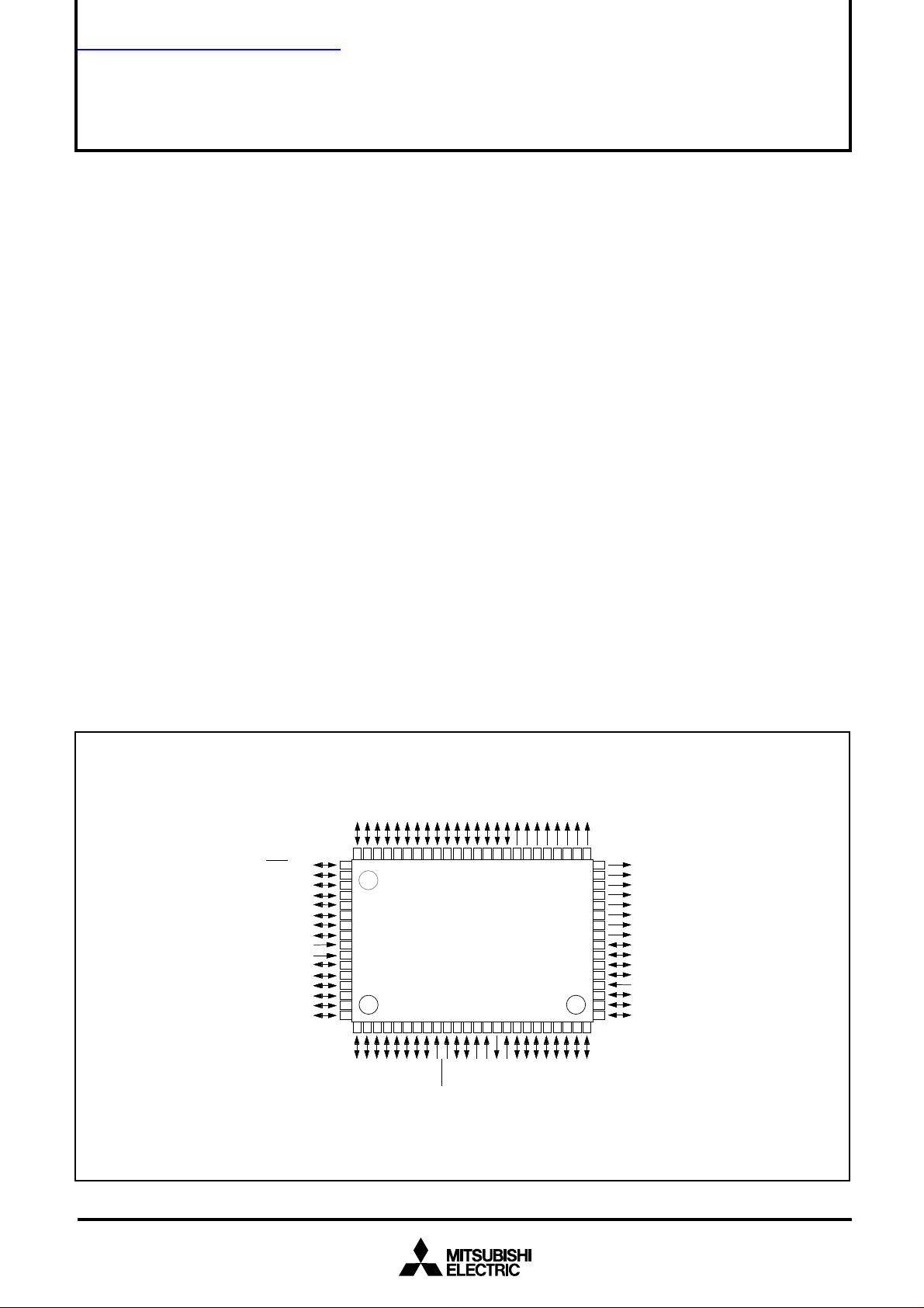
PIN CONFIGURATION (TOP VIEW)
O U T 1
R E F
/ A N
6 5
6 6
6 7
6 8
6 9
7 0
7 1
7 2
I N 1
7 3
S S
7 4
7 5
1 1
7 6
1 0
7 7
9
7 8
8
7 9
7
8 0
6
N o t e : I n t h e m a s k o p t i o n t y p e P , I N T3 a n d C N T R1 c a n n o t b e u s e d .
P 57/ S
R D Y 2 /SC L K 2 2
6
/ S
C L K 2 1
P 5
5
/ T x D
P 5
P 54/ R x D
P 53/ S
C L K 1 2
P 52/ S
C L K 1 1
P 51/ S
P 50/ S
A V
V
P 65/ S
S T B 1
P 62/ S
B U S Y 1
R D Y 1
/ A N
/ A N
P 63/ A N
P 77/ A N
P 76/ A N
P 64/ I N T4/ S
Fig. 1 Pin configuration of M38B4xMxH-XXXXFP
0
D
/
2
1
2
3
4
5
6
7
8
D
D
D
D
U
B
/
/
/
/
/
0
1
2
3
4
2
2
2
2
Z 0
F L
2
F L
P
P
F L
F L
F L
F L
P
P
P
4
96
06
16
26
36
9
D
D
D
D
D
/
/
/
/
/
5
6
7
0
1
2
2
2
0
0
F L
F L
F L
F L
F L
P
P
P
P
P
45
55
65
75
85
M 3 8 B 4 x M x H - X X X X F P
123456789
1
5
4
3
2
N
N
N
N
N
/
/
/
/
/
1
5
4
3
2
7
7
7
7
7
P
P
P
P
P
A
A
A
A
A
A
1
01
11
2
0
1
2
T
T
N
R
R
/
/
0
7
7
4
R
E S E
/
/
P
0
0
P
I N
6
R
O U
P
C N T
)
/
1
6
(
N o t e
C N T
P
C N T
Package type : 80P6N-A
80-pin plastic-molded QFP
0
1
D
/
2
0
F L
P
35
21
T
C
X
/
1
I
9
P
1
1
D
/
3
0
F L
P
25
31
N
C
X
/
0
9
P
2
1
D
/
4
0
F L
P
15
41
S
S
V
3
1
D
/
5
0
P
N
I
X
U
4
1
D
/
6
0
F L
P
05
51
T
O
X
F L
95
61
C
C
V
O U
5
1
D
/
7
0
F L
P
84
71
6
1
D
/
0
1
F L
P
74
81
T
3
T
/
6
4
P
U
T
7
1
D
/
1
1
F L
P
64
92
T
O
1
/
5
4
P
P W
8
1
D
/
2
1
F L
P
54
02
1
M
/
4
4
Z 0
P
9
1
D
/
3
1
F L
P
44
12
1
U
B
/
3
4
I N
P
N o t e
0
2
D
/
4
1
P
3
T
/
2
4
P
)
(
F L
34
22
I N
1
2
D
/
5
1
F L
P
24
32
1
T
/
1
4
P
I N
2
3
2
2
D
D
/
/
6
7
1
1
F L
P
P
4
14
4 0
P 30/ F L D
3 9
3 8
3 7
3 6
3 5
3 4
3 3
3 2
3 1
3 0
2 9
2 8
2 7
2 6
2 5
4
0
9
3
T
D
/
0
/
4
0
P
M
/
7
8
P
F L
P W
2 4
P 31/ F L D
2 5
P 32/ F L D
2 6
P 33/ F L D
2 7
P 34/ F L D
2 8
P 35/ F L D
2 9
P 36/ F L D
3 0
P 37/ F L D
3 1
P 80/ F L D
3 2
P 81/ F L D
3 3
P 82/ F L D
3 4
P 83/ F L D
3 5
V
E E
P 84/ F L D
3 6
P 85/ R T P0/ F L D
P 86/ R T P1/ F L D
3 7
3 8

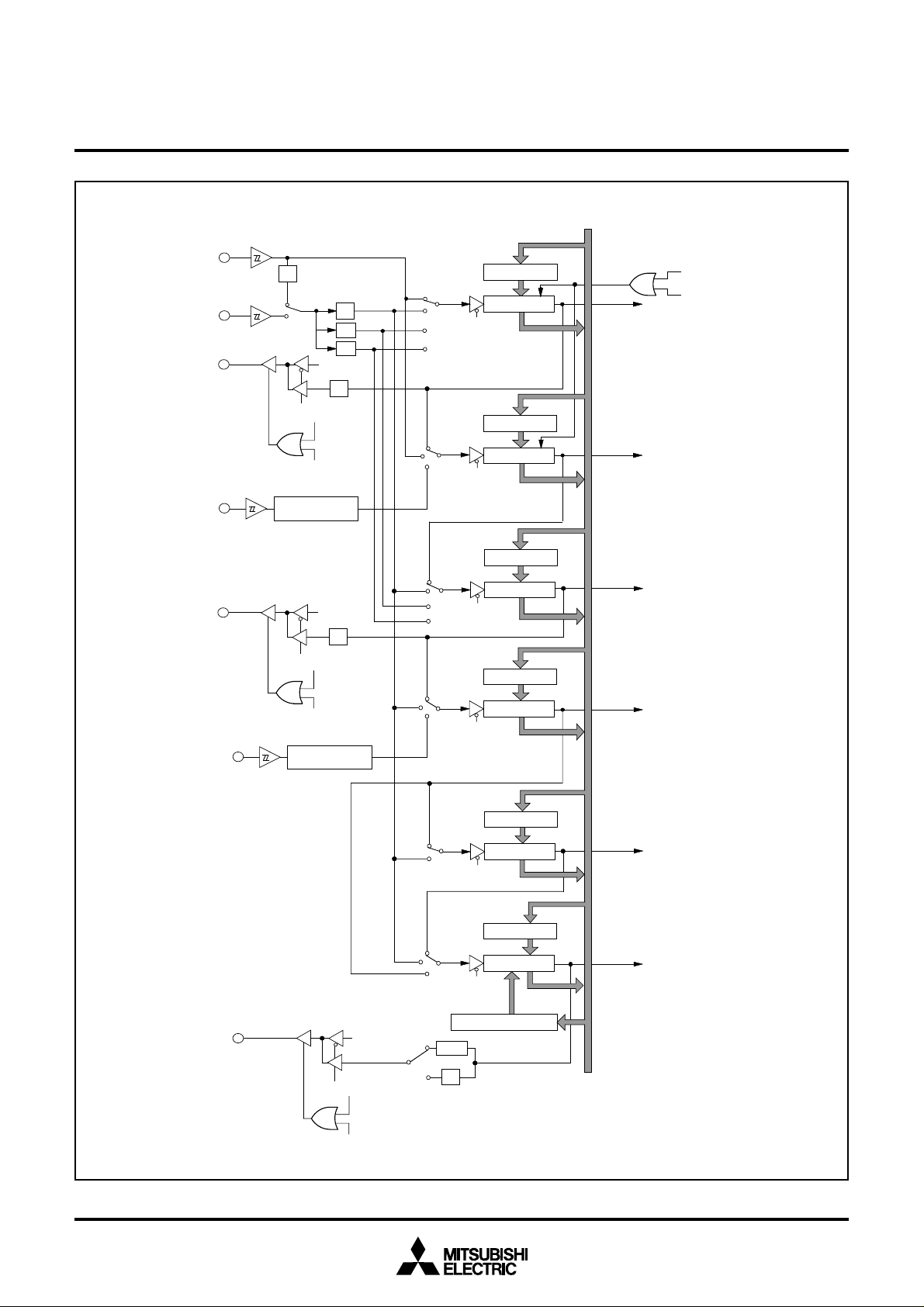
FUNCTIONAL BLOCK
P
o r t P 0 ( 8 )8P o r t P 1 ( 8 )8P o r t P 2 ( 8 )8P o r t P 3 ( 8 )8P o r t P 4 ( 8 )7P o r t P 5 ( 8 )8P o r t P 6 ( 6 )6P o r t P 7 ( 8 )8P o r t P 8 ( 8 )8P o r t P 9 ( 2 )2S y s t e m c l o c k g e n e r a t i o
n
XI
N-
XO
U
T
(
m a i n - c l o c k
)
X
C
I
N-
XC
O U
T
(
s u b - c l o c k
)
T
i m e r
s
T
i m e r X ( 1 6 - b i t
)
T
i m e r 1 ( 8 - b i t
)
T
i m e r 2 ( 8 - b i t
)
T
i m e r 3 ( 8 - b i t
)
T
i m e r 4 ( 8 - b i t
)
T
i m e r 5 ( 8 - b i t
)
T
i m e r 6 ( 8 - b i t
)
A
-
D
c
o
n
v
e
r
t
e
r
(
1
0
-
b
i
t
5
1
2
c
h
a
n
n
e
l
)
C
P U c o r
e
W
a t c h d o g t i m e rR
O MR
A
M
B
u i l d - i n p e r i p h e r a l f u n c t i o n sM
e m o r yI
/ O p o r t
s
P
W M 0 ( 1 4 - b i t
)
P
W
M
1
(
8
-
b
i
t
)
S
e r i a l I /
O
S
e r i a l I / O 1 ( C l o c k - s y n c h r o n i z e d
)
(
2 5 6 b y t e a u t o m a t i c t r a n s f e r
)
S
e
r
i
a
l
I
/
O
2
(
C
l
o
c
k
-
s
y
n
c
h
r
o
n
i
z
e
d
o
r
U
A
R
T
)
F
L D d i s p l a y f u n c t i o
n
4
0
c
o
n
t
r
o
l
p
i
n
s
(
3 6 h i g h - b r e a k d o w n
v
o l t a g e p o r t s
)
I
n t e r r u p t i n t e r v a l d
e t e r m i n a t i o n f u n c t i o n1B u z z e r o u t p u
t
MITSUBISHI MICROCOMPUTERS
38B4 Group
SINGLE-CHIP 8-BIT CMOS MICROCOMPUTER
FUNCTIONAL BLOCK DIAGRAM (Package : 80P6N-A)
Fig. 2 Functional block diagram
2
MITSUBISHI MICROCOMPUTERS
38B4 Group
SINGLE-CHIP 8-BIT CMOS MICROCOMPUTER
PIN DESCRIPTION
Table 1 Pin description (1)
Pin Name Function
VCC, VSS Power source • Apply voltage of 4.0–5.5 V to VCC, and 0 V to VSS.
VEE Pull-down • Apply voltage supplied to pull-down resistors of ports P0, P1, and P3.
power source
VREF Reference • Reference voltage input pin for A-D converter.
voltage
AVSS Analog power • Analog power source input pin for A-D converter.
source • Connect to VSS.
RESET Reset input • Reset input pin for active “L”.
XIN Clock input • Input and output pins for the main clock generating circuit.
• Feedback resistor is built in between XIN pin and XOUT pin.
XOUT Clock output
P00/FLD8– I/O port P0 • 8-bit I/O port. • FLD automatic display
P07/FLD15 • I/O direction register allows each pin to be individually programmed as either pins
P10/FLD16– Output port P1 • 8-bit output port. • FLD automatic display
P17/FLD23 • A pull-down resistor is built in between port P1 and the VEE pin. pins
P20/BUZ02/ I/O port P2 • 8-bit I/O port with the same function as port P0. • FLD automatic display
FLD0– • Low-voltage input level. pins
P27/FLD7 • High-breakdown-voltage P-channel open-drain output structure. • Buzzer output pin (P20)
P30/FLD24– Output port P3 • 8-bit output port. • FLD automatic display
P37/FLD31 • A pull-down resistor is built in between port P3 and the VEE pin. pins
P40/INT0, I/O port P4 • 7-bit I/O port with the same function as port P0. • Interrupt input pins
P41/INT1, • CMOS compatible input level In the mask option type P,
P42/INT3 • N-channel open-drain output structure. INT3 cannot be used.
P43/BUZ01 • Buzzer output pin
P44/PWM1 • PWM output pin
P45/T1OUT, • Timer output pin
P46/T3OUT
P47/INT2 Input port P4 • 1-bit input port. • Interrupt input pin
• Connect a ceramic resonator or quartz-crystal oscillator between the XIN and XOUT pins to set the
oscillation frequency.
• When an external clock is used, connect the clock source to the XIN pin and leave the XOUT pin open.
• The clock is used as the oscillating source of system clock.
input or output.
• At reset, this port is set to input mode.
• A pull-down resistor is built in between port P0 and the VEE pin.
• CMOS compatible input level.
• High-breakdown-voltage P-channel open-drain output structure.
• At reset, this port is set to VEE level.
• High-breakdown-voltage P-channel open-drain output structure.
• At reset, this port is set to VEE level.
• High-breakdown-voltage P-channel open-drain output structure.
• At reset, this port is set to VEE level.
• CMOS compatible input level.
Function except a port function
(Timer output pin)
3

MITSUBISHI MICROCOMPUTERS
38B4 Group
SINGLE-CHIP 8-BIT CMOS MICROCOMPUTER
Table 2 Pin description (2)
Pin Name Function
P50/SIN1, I/O port P5 • 8-bit CMOS I/O port with the same function as port P0. • Serial I/O1 function pins
P51/SOUT1, • CMOS compatible input level.
P52/SCLK11, • CMOS 3-state output structure.
P53/SCLK12
P54/RXD, • Serial I/O2 function pins
P55/TXD,
P56/SCLK21,
P57/SRDY2/
SCLK22
P60/CNTR1 I/O port P6 • 1-bit I/O port with the same function as port P0. • Timer input pin
• CMOS compatible input level. In the mask option type P,
• N-channel open-drain output structure. CNTR1 cannot be used.
P61/CNTR0/ • 5-bit CMOS I/O port with the same function as port P0. • Timer I/O pin
CNTR2 • CMOS compatible input level.
P62/SRDY1/ • CMOS 3-state output structure. • Serial I/O1 function pin
AN8 • A-D conversion input pin
P63/AN9 • A-D conversion input pin
P64/INT4/ • Serial I/O1 function pin
SBUSY1/AN10,
P65/SSTB1/ • Interrupt input pin (P64)
AN11
P70/AN0– I/O port P7 • 8-bit CMOS I/O port with the same function as port P0. •
P77/AN7 • CMOS compatible input level.
• CMOS 3-state output structure.
P80/FLD32– I/O port P8 • 4-bit I/O port with the same function as port P0.
P83/FLD35
P84/FLD36 • 4-bit CMOS I/O port with the same function as port P0.
P85/RTP0/ • Low-voltage input level.
FLD37, • CMOS 3-state output structure • Real time port output
P86/RTP1/
FLD38
P87/PWM0/
FLD39 • 14-bit PWM output
P90/XCIN, I/O port P9 • 2-bit CMOS I/O port with the same function as port P0. •
P91/XCOUT • CMOS compatible input level.
• Low-voltage input level.
• High-breakdown-voltage P-channel open-drain output structure.
• CMOS 3-state output structure.
Function except a port function
•
Dimmer signal output pin
• A-D conversion input pin
A-D conversion input pin
•
FLD automatic display pins
•
FLD automatic display pins
•
FLD automatic display pins
I/O pins for sub-clock generating
circuit (connect a ceramic resona-
tor or a quarts-crystal oscillator)
4

PART NUMBERING
g
y
MITSUBISHI MICROCOMPUTERS
38B4 Group
SINGLE-CHIP 8-BIT CMOS MICROCOMPUTER
P r o d u c t
M 3 8 B 4 9 M F H - X X X X F P
P a c k a g e t y p e
F P : 8 0 P 6 N - A p a c k a
R O M n u m b e r
H i g h - b r e a k d o w n v o l t a g e p u l l - d o w n o p t i o n
R e g a r d i n g o p t i o n c o n t e n t s , r e f e r t o s e c t i o n
“ M A S K O P T I O N O F P U L L - D O W N
R E S I S T O R ” .
R O M s i z e
t e
: 4 0 9 6 b y t e s
1
: 8 1 9 2 b y t e s
2
: 1 2 2 8 8 b y t e s
3
: 1 6 3 8 4 b y t e s
4
: 2 0 4 8 0 b y t e s
5
: 2 4 5 7 6 b y t e s
6
: 2 8 6 7 2 b y t e s
7
: 3 2 7 6 8 b y t e s
8
: 3 6 8 6 4 b y t e s
9
: 4 0 9 6 0 b y t e s
A
: 4 5 0 5 6 b y t e s
B
: 4 9 1 5 2 b y t e s
C
: 5 3 2 4 8 b y t e s
D
: 5 7 3 4 4 b y t e s
E
: 6 1 4 4 0 b
F
s
e
Fig. 3 Part numbering
T h e f i r s t 1 2 8 b y t e s a n d t h e l a s t 2 b y t e s o f R O M
a r e r e s e r v e d a r e a s ; t h e y c a n n o t b e u s e d f o r
u s e r s .
M e m o r y t y p e
: M a s k R O M v e r s i o n
M
: E P R O M o r O n e T i m e P R O M v e r s i o n
E
R A M s i z e
0
: 1 9 2 b y t e s
: 2 5 6 b y t e s
1
: 3 8 4 b y t e s
2
: 5 1 2 b y t e s
3
: 6 4 0 b y t e s
4
: 7 6 8 b y t e s
5
: 8 9 6 b y t e s
6
: 1 0 2 4 b y t e s
7
: 1 5 3 6 b y t e s
8
: 2 0 4 8 b y t e s
9
5
GROUP EXPANSION
Mitsubishi plans to expand the 38B4 group as follows:
Memory Type
Support for Mask ROM version.
Memory Size
Mask ROM size..................................................... 48K to 60K bytes
RAM size............................................................1024 to 2048 bytes
Package
80P6N-A ..................................... 0.8 mm-pitch plastic molded QFP
MITSUBISHI MICROCOMPUTERS
38B4 Group
SINGLE-CHIP 8-BIT CMOS MICROCOMPUTER
R O M s i z e ( b y t e s )
6 0 K
5 6 K
5 2 K
4 8 K
4 4 K
4 0 K
3 6 K
3 2 K
2 8 K
2 4 K
2 0 K
1 6 K
1 2 K
8 K
4 K
2 5 65
Note : Products under development or planning : the development schedule and specifications may be revised without notice.
1
27
U n d e r d e v e l o p m e n t
M 3 8 B 4 7 MC
6
81
, 0 2
R A M s i z e ( b y t e s )
41
, 5 3
62
U n d e r d e v e l o p m e n t
M 3 8 B 4 9 M F H
, 0 4
8
Fig. 4 Memory expansion plan
Currently supported products are listed below.
Table 3 List of supported products
Product
M38B49MFH-XXXXFP
M38B47MCH-XXXXFP
6
ROM size (bytes)
ROM size for User ( )
61440
(61310)
49152
(49022)
RAM size (bytes)
2048
1024
Package
80P6N-A
80P6N-A
As of Mar. 2000
Remarks
Mask ROM version
Mask ROM version

MITSUBISHI MICROCOMPUTERS
38B4 Group
SINGLE-CHIP 8-BIT CMOS MICROCOMPUTER
FUNCTIONAL DESCRIPTION
Central Processing Unit (CPU)
The 38B4 group uses the standard 740 Family instruction set. Refer to the table of 740 Family addressing modes and machine
instructions or the 740 Family Software Manual for details on the
instruction set.
Machine-resident 740 Family instructions are as follows:
The FST and SLW instructions cannot be used.
The STP, WIT, MUL, and DIV instr uctions can be used.
[Accumulator (A)]
The accumulator is an 8-bit register. Data operations such as data
transfer, etc., are executed mainly through the accum ulator.
[Index Register X (X)]
The index register X is an 8-bit register. In the index addressing
modes, the value of the OPERAND is added to the contents of
register X and specifies the real address.
[Index Register Y (Y)]
The index register Y is an 8-bit register. In partial instruction, the
value of the OPERAND is added to the contents of register Y and
specifies the real address.
[Stack Pointer (S)]
The stack pointer is an 8-bit register used during subroutine calls
and interrupts. This register indicates start address of stored area
(stack) for storing registers during subroutine calls and interrupts.
The low-order 8 bits of the stack address are determined by the
contents of the stack pointer. The high-order 8 bits of the stack address are determined by the stack page selection bit. If the stack
page selection bit is “0” , the high-order 8 bits becomes “0016”. If
the stack page selection bit is “1”, the high-order 8 bits becomes
“0116”.
The operations of pushing register contents onto the stack and
popping them from the stack are shown in Figure 6.
Store registers other than those described in Figure 6 with program when the user needs them during interrupts or subroutine
calls (see Table 4).
[Program Counter (PC)]
The program counter is a 16-bit counter consisting of two 8-bit
registers PCH and PCL. It is used to indicate the address of the
next instruction to be executed.
b7
b0
A Accumulator
b7
b0
X Index register X
b7
b0
Y Index register Y
b7 b0
S Stack pointer
b7b15 b0
PC
H
L
Program counterPC
b7 b0
N V T B D I Z C Processor status register (PS)
Carry flag
Zero flag
Interrupt disable flag
Decimal mode flag
Break flag
Index X mode flag
Overflow flag
Negative flag
Fig. 5 740 Family CPU register structure
7

e
O n - g o i n g R o u t i n
MITSUBISHI MICROCOMPUTERS
38B4 Group
SINGLE-CHIP 8-BIT CMOS MICROCOMPUTER
P u s h r e t u r n a d d r e s s
o n s t a c k
P O P re t u r n
a d d r e s s f r o m s t a c k
I n t e r r u p t r e q u e s t
M ( S )( P CH)
( S )
M ( S )( P CL)
( S )
S u b r o u t i n e
E x e c u t e R T S
( S )
( P CL)M ( S )
( S )
( P CH)M ( S )
( N o t e )
( S ) – 1
( S ) – 1
( S ) + 1
( S ) + 1
E x e c u t e J S R
M ( S )( P CH)
( S )
( S ) – 1
M ( S )( P CL)
( S )
( S ) – 1
M ( S )( P S )
( S )
( S ) – 1
I n t e r r u p t
S e r v i c e R o u t i n e
E x e c u t e R T I
( S )
( S ) + 1
( P S )M ( S )
( S )
( S ) + 1
( P CL)M ( S )
( S )
( S ) + 1
P u s h r e t u r n a d d r e s s
o n s t a c k
P u s h c o n t e n t s o f p r o c e s s o r
s t a t u s r e g i s t e r o n s t a c k
I F l a g i s s e t f r o m “ 0 ” t o “ 1 ”
F e t c h t h e j u m p v e c t o r
P O P c o n t e n t s o f
p r o c e s s o r s t a t u s
r e g i s t e r f r o m s t a c k
P O P r e t u r n
a d d r e s s
f r o m s t a c k
( P CH)M ( S )
N o t e: C o n d i t i o n f o r a c c e p t a n c e o f a n i n t e r r u p t I n t e r r u p t e n a b l e f l a g i s “ 1 ”
Fig. 6 Register push and pop at interrupt generation and subroutine call
Table 4 Push and pop instructions of accumulator or processor status register
Push instruction to stack
Accumulator
Processor status register
PHA
PHP
I n t e r r u p t d i s a b l e f l a g i s “ 0 ”
Pop instruction from stack
PLA
PLP
8

MITSUBISHI MICROCOMPUTERS
38B4 Group
SINGLE-CHIP 8-BIT CMOS MICROCOMPUTER
[Processor Status Register (PS)]
The processor status register is an 8-bit register consisting of 5
flags which indicate the status of the processor after an arithmetic
operation and 3 flags which decide MCU operation. Branch operations can be performed by testing the Carry (C) flag , Zero (Z) flag,
Overflow (V) flag, or the Negative (N) flag. In decimal mode, the Z,
V, N flags are not valid.
•Bit 0: Carry flag (C)
The C flag contains a carry or borrow generated by the arithmetic
logic unit (ALU) immediately after an arithmetic operation. It can
also be changed by a shift or rotate instruction.
•Bit 1: Zero flag (Z)
The Z flag is set if the result of an immediate arithmetic operation
or a data transfer is “0”, and cleared if the result is anything other
than “0”.
•Bit 2: Interrupt disable flag (I)
The I flag disables all interrupts except for the interrupt
generated by the BRK instruction.
Interrupts are disabled when the I flag is “1”.
•Bit 3: Decimal mode flag (D)
The D flag determines whether additions and subtractions are
executed in binary or decimal. Binary arithmetic is executed when
this flag is “0”; decimal arithmetic is executed when it is “1”.
Decimal correction is automatic in decimal mode. Only the ADC
and SBC instructions can be used for decimal arithmetic.
•Bit 4: Break flag (B)
The B flag is used to indicate that the current interrupt was
generated by the BRK instruction. The BRK flag in the processor
status register is always “0”. When the BRK instruction is used to
generate an interrupt, the processor status register is pushed
onto the stack with the break flag set to “1”.
•Bit 5: Index X mode flag (T)
When the T flag is “0”, arithmetic operations are performed
between accumulator and memory. When the T flag is “1”, direct
arithmetic operations and direct data transfers are enabled
between memory locations.
•Bit 6: Overflow flag (V)
The V flag is used during the addition or subtraction of one byte
of signed data. It is set if the result exceeds +127 to -128. When
the BIT instruction is executed, bit 6 of the memory location
operated on by the BIT instruction is stored in the overflow flag.
•Bit 7: Negative flag (N)
The N flag is set if the result of an arithmetic operation or data
transfer is negative. When the BIT instruction is executed, bit 7 of
the memory location operated on by the BIT instruction is stored
in the negative flag.
Table 5 Set and clear instructions of each bit of processor status register
C flag Z flag I flag D flag B flag T flag V flag N flag
Set instruction
Clear instruction
SEC
CLC
_
_
SEI
CLI
SED
CLD
_
_
SET
CLT CLV
_
_
_
9
[CPU Mode Register (CPUM)] 003B16
The CPU mode register contains the stack page selection bit and
the internal system clock selection bit etc.
The CPU mode register is allocated at address 003B16.
MITSUBISHI MICROCOMPUTERS
38B4 Group
SINGLE-CHIP 8-BIT CMOS MICROCOMPUTER
b 7
b 0
C P U m o d e r e g i s t e r
(
C P U M : a d d r e s s
P r o c e s s o r m o d e b i t s
b 1 b 0
0 0 : S i n g l e - c h i p m o d e
0 1 :
1 0 : N o t a v a i l a b l e
1 1 :
S t a c k p a g e s e l e c t i o n b i t
0 : P a g e 0
1 : P a g e 1
N o t a v a i l a b l e
P o r t X
C
0 : I / O p o r t f u n c t i o n
1 : X
C I N
M a i n c l o c k ( X
0 : O s c i l l a t i n g
1 : S t o p p e d
M a i n c l o c k d i v i s i o n r a t i o s e l e c t i o n b i t
0 : f ( X
1 : f ( X
I n t e r n a l s y s t e m c l o c k s e l e c t i o n b i t
0 : X
1 : X
Fig. 7 Structure of CPU mode register
0 0 3 B
1 6
)
s w i t c h b i t
– X
C O U T
o s c i l l a t i n g f u n c t i o n
I N
– X
O U T
) s t o p b i t
I N
) ( h i g h - s p e e d m o d e )
I N
) / 4 ( m i d d l e - s p e e d m o d e )
I N
- X
O U T
s e l e c t i o n ( m i d d l e - / h i g h - s p e e d m o d e )
C I N
- X
C O U T
s e l e c t i o n ( l o w - s p e e d m o d e )
10
MITSUBISHI MICROCOMPUTERS
6
6
6
6
a
38B4 Group
SINGLE-CHIP 8-BIT CMOS MICROCOMPUTER
MEMORY
Special Function Register (SFR) Area
The special function register (SFR) area in the zero page contains
control registers such as I/O ports and timers.
RAM
RAM is used for data storage and for stack area of subroutine calls
and interrupts.
ROM
The first 128 bytes and the last 2 bytes of ROM are reserved for
device testing, and the other areas are user areas for storing programs.
Interrupt Vector Area
The interrupt vector area contains reset and interrupt vectors.
R A M a r e a
R A M s i z e
( b y t e )
1 9 2
2 5 6
3 8 4
5 1 2
6 4 0
7 6 8
8 9 6
1 0 2 4
1 5 3 6
2 0 4 8
R O M a r e a
R O M s i z e
( b y t e )
4 0 9 6
8 1 9 2
1 2 2 8 8
1 6 3 8 4
2 0 4 8 0
2 4 5 7 6
2 8 6 7 2
3 2 7 6 8
3 6 8 6 4
4 0 9 6 0
4 5 0 5 6
4 9 1 5 2
5 3 2 4 8
5 7 3 4 4
6 1 4 4 0
A d d r e s s
X X X X
0 0 F F
0 1 3 F
0 1 B F
0 2 3 F
0 2 B F
0 3 3 F
0 3 B F
0 4 3 F
0 6 3 F
0 8 3 F
A d d r e s s
Y Y Y Y
F 0 0 0
E 0 0 0
D 0 0 0
C 0 0 0
B 0 0 0
A 0 0 0
9 0 0 0
1 6
8 0 0 0
1 6
7 0 0 0
1 6
6 0 0 0
1 6
5 0 0 0
1 6
4 0 0 0
1 6
3 0 0 0
1 6
2 0 0 0
1 6
1 0 0 0
1 6
1 6
1 6
1 6
1 6
1 6
1 6
1 6
1 6
1 6
1 6
1 6
A d d r e s s
1 6
1 6
1 6
1 6
1 6
1 6
1 6
Z Z Z Z
F 0 8 0
E 0 8 0
D 0 8 0
C 0 8 0
B 0 8 0
A 0 8 0
9 0 8 0
8 0 8 0
7 0 8 0
6 0 8 0
5 0 8 0
4 0 8 0
3 0 8 0
2 0 8 0
1 0 8 0
1 6
1 6
1 6
1 6
1 6
1 6
1 6
1 6
1 6
1 6
1 6
1 6
1 6
1 6
1 6
1 6
Zero Page
The 256 bytes from addresses 000016 to 00FF16 are called the zero
page area. The internal RAM and the special function registers (SFR)
are allocated to this area.
The zero page addressing mode can be used to specify memory and
register addresses in the zero page area. Access to this area with
only 2 bytes is possible in the zero page addressing mode.
Special Page
The 256 bytes from addresses FF0016 to FFFF16 are called the special page area. The special page addressing mode can be used to
specify memory addresses in the special page area. Access to this
area with only 2 bytes is possible in the special page addressing
mode.
0 0 0 0
R A M
R O M
0 0 4 0
0 1 0 0
X X X X
0 4 4 0
0 E F 0
0 E F F
0 F 0 0
0 F F F
Y Y Y Y
Z Z Z Z
F F 0 0
F F D C
F F F E
F F F F
1 6
1 6
1 6
1 6
1
1
1
1 6
1
1 6
1 6
1 6
1 6
1 6
1 6
S F R a r e a 1
R e s e r v e d a r e a
N o t u s e d ( N o t e )
S F R a r e a 2
R A M a r e a f o r S e r i a l I / O a u t o m a t i c
t r a n s f e r
R A M a r e a f o r F L D a u t o m a t i c d i s p l a y
R e s e r v e d R O M a r e a
( c o m m o n R O M a r e a , 1 2 8 b y t e )
I n t e r r u p t v e c t o r a r e a
R e s e r v e d R O M a r e
Z e r o p a g e
S p e c i a l p a g e
Fig. 8 Memory map diagram
N o t e: W h e n 1 0 2 4 b y t e s o r m o r e a r e u s e d a s R A M a r e a , t h i s a r e a c a n b e u s e d .
11
MITSUBISHI MICROCOMPUTERS
S
C O
38B4 Group
SINGLE-CHIP 8-BIT CMOS MICROCOMPUTER
0 0 0 0
0 0 0 1
0 0 0 2
0 0 0 3
0 0 0 4
0 0 0 5
0 0 0 6
0 0 0 7
0 0 0 8
0 0 0 9
0 0 0 A
0 0 0 B
0 0 0 C
0 0 0 D
0 0 0 E
0 0 0 F
0 0 1 0
0 0 1 1
0 0 1 2
0 0 1 3
0 0 1 4
0 0 1 5
0 0 1 6
0 0 1 7
0 0 1 8
0 0 1 9
0 0 1 A
0 0 1 B
0 0 1 C
0 0 1 D
0 0 1 E
0 0 1 F
1 6
P o r t P 0 ( P 0 )
P o r t P 0 d i r e c t i o n r e g i s t e r ( P 0 D )
1 6
P o r t P 1 ( P 1 )
1 6
1 6
P o r t P 2 ( P 2 )
1 6
P o r t P 2 d i r e c t i o n r e g i s t e r ( P 2 D )
1 6
P o r t P 3 ( P 3 )
1 6
1 6
P o r t P 4 ( P 4 )
1 6
P o r t P 4 d i r e c t i o n r e g i s t e r ( P 4 D )
1 6
P o r t P 5 ( P 5 )
1 6
P o r t P 5 d i r e c t i o n r e g i s t e r ( P 5 D )
1 6
P o r t P 6 ( P 6 )
1 6
P o r t P 6 d i r e c t i o n r e g i s t e r ( P 6 D )
1 6
P o r t P 7 ( P 7 )
1 6
P o r t P 7 d i r e c t i o n r e g i s t e r ( P 7 D )
1 6
P o r t P 8 ( P 8 )
1 6
P o r t P 8 d i r e c t i o n r e g i s t e r ( P 8 D )
1 6
P o r t P 9 ( P 9 )
1 6
P o r t P 9 d i r e c t i o n r e g i s t e r ( P 9 D )
1 6
P W M r e g i s t e r ( h i g h - o r d e r ) ( P W M H )
1 6
P W M r e g i s t e r ( l o w - o r d e r ) ( P W M L )
1 6
B a u d r a t e g e n e r a t o r ( B R G )
1 6
U A R T c o n t r o l r e g i s t e r ( U A R T C O N )
1 6
1 6
S e r i a l I / O 1 a u t o m a t i c t r a n s f e r d a t a p o i n t e r ( S I O 1 D P )
S e r i a l I / O 1 c o n t r o l r e g i s t e r 1 ( S I O 1 C O N 1 )
1 6
1 6
S e r i a l I / O 1 c o n t r o l r e g i s t e r 2 ( S I O 1 C O N 2 )
1 6
S e r i a l I / O 1 r e g i s t e r / T r a n s f e r c o u n t e r ( S I O 1 )
S e r i a l I / O 1 c o n t r o l r e g i s t e r 3 ( S I O 1 C O N 3 )
1 6
S e r i a l I / O 2 c o n t r o l r e g i s t e r ( S I O 2 C O N )
1 6
1 6
S e r i a l I / O 2 s t a t u s r e g i s t e r ( S I O 2 S T S )
e r i a l I / O 2 t r a n s m i t / r e c e i v e b u f f e r r e g i s t e r ( T B / R B
1 6
0 0 2 0
0 0 2 1
0 0 2 2
0 0 2 3
0 0 2 4
0 0 2 5
0 0 2 6
0 0 2 7
0 0 2 8
0 0 2 9
0 0 2 A
0 0 2 B
0 0 2 C
0 0 2 D
0 0 2 E
0 0 2 F
0 0 3 0
0 0 3 1
0 0 3 2
0 0 3 3
0 0 3 4
0 0 3 5
0 0 3 6
0 0 3 7
0 0 3 8
0 0 3 9
0 0 3 A
0 0 3 B
0 0 3 C
0 0 3 D
0 0 3 E
)
0 0 3 F
T i m e r 1 ( T 1 )
1 6
T i m e r 2 ( T 2 )
1 6
T i m e r 3 ( T 3 )
1 6
T i m e r 4 ( T 4 )
1 6
T i m e r 5 ( T 5 )
1 6
T i m e r 6 ( T 6 )
1 6
P W M c o n t r o l r e g i s t e r ( P W M C O N )
1 6
T i m e r 6 P W M r e g i s t e r ( T 6 P W M )
1 6
T i m e r 1 2 m o d e r e g i s t e r ( T 1 2 M )
1 6
T i m e r 3 4 m o d e r e g i s t e r ( T 3 4 M )
1 6
T i m e r 5 6 m o d e r e g i s t e r ( T 5 6 M )
1 6
W a t c h d o g t i m e r c o n t r o l r e g i s t e r ( W D T C O N )
1 6
T i m e r X ( l o w - o r d e r ) ( T X L )
1 6
T i m e r X ( h i g h - o r d e r ) ( T X H )
1 6
1 6
T i m e r X m o d e r e g i s t e r 1 ( T X M 1 )
T i m e r X m o d e r e g i s t e r 2 ( T X M 2 )
1 6
I n t e r r u p t i n t e r v a l d e t e r m i n a t i o n r e g i s t e r ( I I D )
1 6
I n t e r r u p t i n t e r v a l d e t e r m i n a t i o n c o n t r o l r e g i s t e r ( I I D C O N )
1 6
1 6
A - D c o n t r o l r e g i s t e r ( A D C O N )
1 6
A - D c o n v e r s i o n r e g i s t e r ( l o w - o r d e r ) ( A D L )
1 6
A - D c o n v e r s i o n r e g i s t e r ( h i g h - o r d e r ) ( A D H )
1 6
1 6
1 6
1 6
I n t e r r u p t s o u r c e s w i t c h r e g i s t e r ( I F R )
1 6
1 6
I n t e r r u p t e d g e s e l e c t i o n r e g i s t e r
1 6
C P U m o d e r e g i s t e r ( C P U M )
I n t e r r u p t r e q u e s t r e g i s t e r 1 ( I R E Q 1 )
1 6
I n t e r r u p t r e q u e s t r e g i s t e r 2 ( I R E Q 2 )
1 6
1 6
I n t e r r u p t c o n t r o l r e g i s t e r 1 ( I C O N 1 )
1 6
I n t e r r u p t c o n t r o l r e g i s t e r 2 ( I C O N 2 )
( I N T E D G E )
0 E F 0
0 E F 1
0 E F 2
0 E F 3
0 E F 4
0 E F 5
0 E F 6
0 E F 7
P u l l - u p c o n t r o l r e g i s t e r 1 ( P U L L 1 )
1 6
P u l l - u p c o n t r o l r e g i s t e r 2 ( P U L L 2 )
1 6
1 6
1 6
F L D C m o d e r e g i s t e r ( F L D M )
1 6
T d i s p t i m e s e t r e g i s t e r ( T D I S P )
1 6
T o f f 1 t i m e s e t r e g i s t e r ( T O F F 1 )
1 6
1 6
T o f f 2 t i m e s e t r e g i s t e r ( T O F F 2 )
0 E F 8
0 E F 9
0 E F A
0 E F B
0 E F C
0 E F D
0 E F E
0 E F F
F L D d a t a p o i n t e r ( F L D D P )
1 6
P o r t P 0 F L D / p o r t s w i t c h r e g i s t e r ( P 0 F P R )
1 6
1 6
P o r t P 2 F L D / p o r t s w i t c h r e g i s t e r ( P 2 F P R )
1 6
P o r t P 8 F L D / p o r t s w i t c h r e g i s t e r ( P 8 F P R )
N
P o r t P 8 F L D o u t p u t c o n t r o l r e g i s t e r ( P 8 F L D
1 6
1 6
B u z z e r o u t p u t c o n t r o l r e g i s t e r ( B U Z C O N )
1 6
1 6
)
Fig. 9 Memory map of special function register (SFR)
12
I/O PORTS
[Direction Registers] PiD
The 38B4 group has 51 programmable I/O pins arranged in eight
individual I/O ports (P0, P2, P40–P46, and P5–P9). The I/O ports
have direction registers which determine the input/output direction of
each individual pin. Each bit in a direction register corresponds to
one pin, and each pin can be set to be input port or output port. When
“0” is written to the bit corresponding to a pin, that pin becomes an
input pin. When “1” is written to that pin, that pin becomes an output
pin. If data is read from a pin set to output, the value of the port
output latch is read, not the value of the pin itself. Pins set to input
(the bit corresponding to that pin must be set to “0”) are floating and
the value of that pin can be read. If a pin set to input is written to, only
the port output latch is written to and the pin remains floating.
[High-Breakdown-Voltage Output Ports]
The 38B4 group has 5 ports with high-breakdown-voltage pins (ports
P0–P3 and P80–P83). The high-breakdown-voltage ports have Pchannel open-drain output with Vcc- 45 V of breakdown voltage. Each
pin in ports P0, P1, and P3 has an internal pull-down resistor connected to VEE. At reset, the P-channel output transistor of each port
latch is turned off, so that it goes to VEE level (“L”) by the pull-down
resistor.
Writing “1” (weak drivability) to bit 7 of the FLDC mode register (address 0EF416) shows the rising transition of the output transistors for
reducing transient noise. At reset, bit 7 of the FLDC mode register is
set to “0” (strong drivability).
[Pull-up Control Register] PULL
Ports P5, P61–P65, P7, P84–P87 and P9 have built-in programmable
pull-up resistors. The pull-up resistors are valid only in the case that
the each control bit is set to “1” and the corresponding port direction
registers are set to input mode.
MITSUBISHI MICROCOMPUTERS
38B4 Group
SINGLE-CHIP 8-BIT CMOS MICROCOMPUTER
b 7
b 7
Fig. 10 Structure of pull-up control registers
PULL2)
b 0
P u l l - u p c o n t r o l r e g i s t e r 1
( P U L L 1 : a d d r e s s 0 E F 0
P 50, P 51 p u l l - u p c o n t r o l b i t
P
2,
53 p u l l - u p c o n t r o l b i t
P 5
P
P 5
4,
55 p u l l - u p c o n t r o l b i t
P
6,
57 p u l l - u p c o n t r o l b i t
P 5
p u l l - u p c o n t r o l b i
1
P 6
P
P 6
2,
63 p u l l - u p c o n t r o l b i t
P
4,
65 p u l l - u p c o n t r o l b i t
P 6
N o t u s e d
( r e t u r n s “ 0 ” w h e n r e a d )
b 0
P u l l - u p c o n t r o l r e g i s t e r 2
( P U L L 2 : a d d r e s s 0 E F 1
P 70, P 71 p u l l - u p c o n t r o l b i t
P
P 7
2,
73 p u l l - u p c o n t r o l b i t
P
4,
75 p u l l - u p c o n t r o l b i t
P 7
P
P 7
6,
77 p u l l - u p c o n t r o l b i t
P
4,
85 p u l l - u p c o n t r o l b i t
P 8
P
6,
87 p u l l - u p c o n t r o l b i t
P 8
P
P 9
0,
91 p u l l - u p c o n t r o l b i t
N o t u s e d
( r e t u r n s “ 0 ” w h e n r e a d )
1
6)
t
1
6)
0 : N o p u l l - u p
1 : P u l l - u p
0 : N o p u l l - u p
1 : P u l l - u p
(PULL1 and
13
MITSUBISHI MICROCOMPUTERS
38B4 Group
SINGLE-CHIP 8-BIT CMOS MICROCOMPUTER
Table 6 List of I/O port functions (1)
zPin Name Input/Output I/O Format Non-Port Function Related SFRs Ref.No.
P00/FLD8– Port P0 Input/output, CMOS compatible input level FLD automatic display function FLDC mode register (1)
P07/FLD15 individual bits High-breakdown voltage P-
channel open-drain output
with pull-down resistor
P10/FLD16– Port P1 Output High-breakdown voltage P- FLDC mode register (2)
P17/FLD23 channel open-drain output
with pull-down resistor
P20/BUZ02/ Port P2 Input/output, Low-voltage input level Buzzer output (P20) FLDC mode register (3)
FLD0 individual bits High-breakdown voltage P- FLD automatic display function
P21/FLD1– channel open-drain output FLD automatic display function
P27/FLD7
P30/FLD24– Port P3 Output High-breakdown voltage P- FLDC mode register (2)
P37/FLD31 channel open-drain output
with pull-down resistor
P40/INT0, Port P4 Input/output, CMOS compatible input level External interrupt input
P41/INT1 individual bits N-channel open-drain output In the mask option type P, INT3
P42/INT3 cannot be used.
P43/BUZ01 Buzzer output
P44/PWM1 PWM output Timer 56 mode register (6)
P45/T1OUT Timer output Timer 12 mode register (8-1)
P46/T3OUT Timer output Timer 34 mode register (8-2)
P47/INT2 Input CMOS compatible input level External interrput input I
P50/SIN1 Port P5 Input/output, CMOS compatible input level Serial I/O1 function I/O
P51/SOUT1, individual bits CMOS 3-state output (11)
P52/SCLK11,
P53/SCLK12
P54/RXD Serial I/O2 function I/O Serial I/O2 control register (10)
P55/TXD, UART control register (11)
P56/SCLK21
P57/SRDY2/ (12)
SCLK22
P60/CNTR1 Port P6 CMOS compatible input level External count input
N-channel open-drain output In the mask option type P, (7-2)
P61/CNTR0/ CMOS compatible input level CNTR1 cannot be used. (13)
CNTR2 CMOS 3-state output
P62/SRDY1/ Serial I/O1 function I/O
AN8 A-D conversion input A-D control register
P63/AN9 A-D conversion input A-D control register (15)
Dimmer signal output P8FLD output control bit
P64/INT4/ Serial I/O1 function I/O
SBUSY1/
AN10
P65/SSTB1/ Serial I/O1 function I/O
AN11 A-D conversion input A-D control register
P70/AN0– Port P7 A-D conversion input A-D control register (15)
P77/AN7
A-D conversion input A-D control register
External interrupt input
Port P0FLD/port switch register
Port P2FLD/port switch register
Buzzer output control register
Interrupt edge selection register
(7-
1) (7-2)
Buzzer output control register
nterrupt edge selection register
Interrupt interval determination
control register
Serial I/O1 control register 1, 2
Interrupt edge selection register
Serial I/O1 control register 1, 2
Serial I/O1 control register 1, 2
Interrupt edge selection register
Serial I/O1 control register 1, 2
(1)
(5)
(4)
(9)
(10)
(7-1)
(14)
(16)
(17)
14
MITSUBISHI MICROCOMPUTERS
38B4 Group
SINGLE-CHIP 8-BIT CMOS MICROCOMPUTER
Table 7 List of I/O port functions (2)
Pin Name Input/Output I/O Format Non-Port Function Related SFRs Ref.No.
P80/FLD32– Port P8 Input/output, Low-voltage input level FLD automatic display function FLDC mode register (1)
P83/FLD35 individual bits High-breakdown voltage P-
channel open-drain output
P84/FLD36 Low-voltage input level (18)
P85/RTP0/ CMOS 3-state output FLD automatic display function FLDC mode register (19)
FLD37, Real time port output
P86/RTP1/ Timer X mode register 2
FLD38
P87/PWM0/ FLD automatic display function FLDC mode register (20)
FLD39 PWM output
P90/XCIN Port P9 CMOS compatible input level Sub-clock generating circuit I/O CPU mode register (21)
P91/XCOUT CMOS 3-state output (22)
Notes 1 : Make sure that the input level at each pin is either 0 V or Vcc during execution of the STP instruction.
When an input level is at an intermediate potential, a current will flow from Vcc to Vss through the input-stage gate.
2 : How to use double-function ports as function I/O ports, refer to the applicable sections.
Port P8FLD/port switch register
Port P8FLD/port switch register
Port P8FLD/port switch register
PWM control register
15
MITSUBISHI MICROCOMPUTERS
38B4 Group
SINGLE-CHIP 8-BIT CMOS MICROCOMPUTER
( 1 ) P o r t s P 0 , P 21– P 27, P 80– P 8
F L D / P o r t
s w i t c h r e g i s t e r
D i m m e r s i g n a l ( N o t e 1 )
L o c a l d a t a
b u s
D a t a b u s
( 3 ) P o r t P 2
L o c a l d a t a
b u s
D a t a b u s
( 5 ) P o r t s P 40, P 4
D i r e c t i o n r e g i s t e r
P o r t l a t c h
0
F L D / P o r t
s w i t c h r e g i s t e r
D i m m e r s i g n a l ( N o t e 1 )
D i r e c t i o n r e g i s t e r
P o r t l a t c h
1
3
B u z z e r c o n t r o l s i g n a l
B u z z e r s i g n a l o u t p u t
r e a d
r e a d
V
E E
*
( N o t e 2 )
V
E E
*
( N o t e 2 )
( 2 ) P o r t s P 1 , P 3
L o c a l d a t a
b u s
D a t a b u s
( 4 ) P o r t P 4
( 6 ) P o r t P 4
3
D a t a b u s
4
T i m e r 6 o u t p u t s e l e c t i o n b i t
D i m m e r s i g n a l ( N o t e 1 )
P o r t l a t c h
D i r e c t i o n r e g i s t e r
P o r t l a t c h
B u z z e r c o n t r o l s i g n a l
B u z z e r s i g n a l o u t p u t
r e a d
*
V
E E
#
D i r e c t i o n r e g i s t e r
D a t a b u s
I N T
0
,
I N T
P o r t l a t c h
1
i n t e r r u p t i n p u t
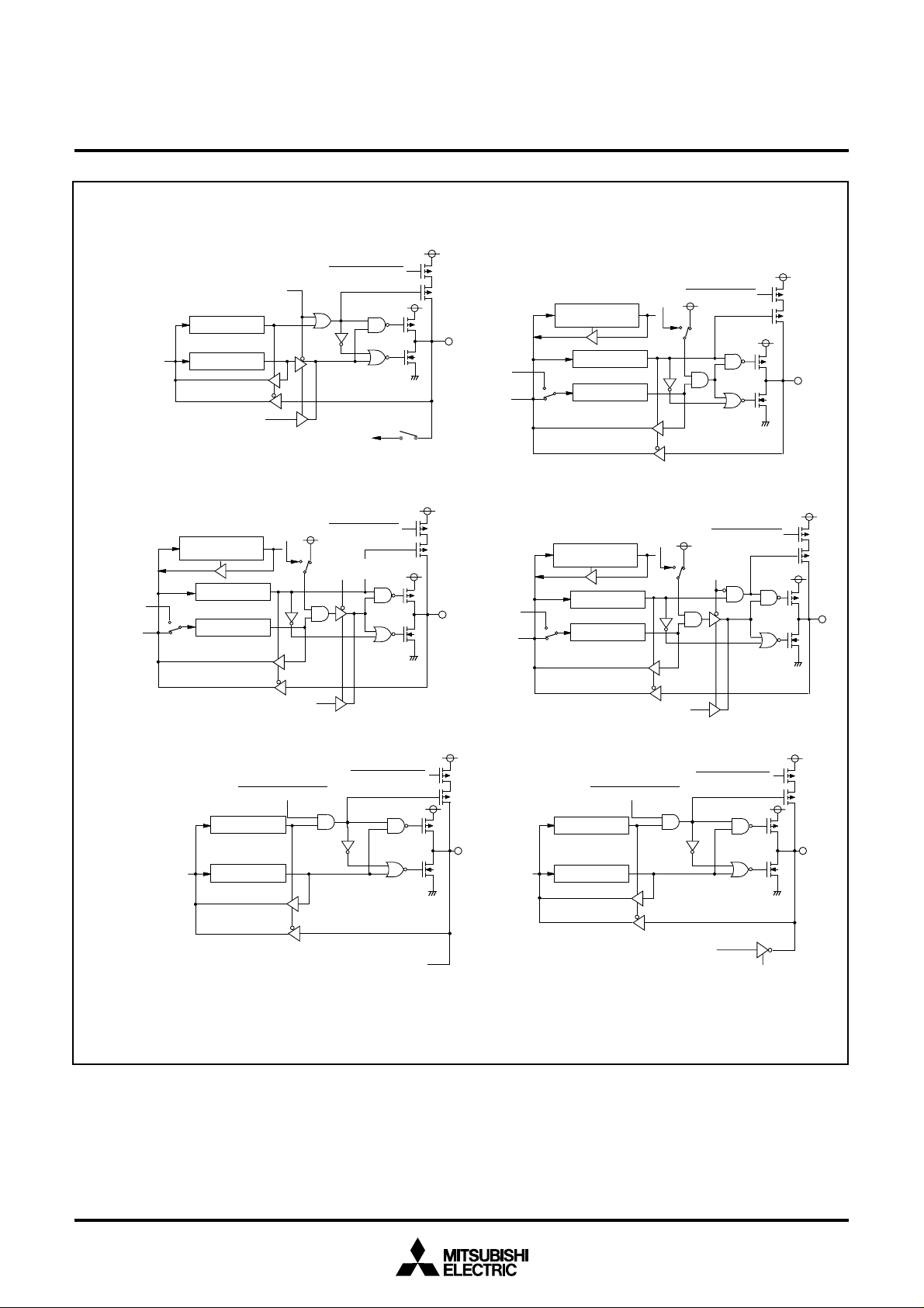
Fig. 11 Port block diagram (1)
D i r e c t i o n r e g i s t e r
D a t a b u s
* H i g h - b r e a k d o w n - v o l t a g e P - c h a n n e l t r a n s i s t o r
# M i d d l e - b r e a k d o w n - v o l t a g e N - c h a n n e l t r a n s i s t o r
N o t e s 1 : T h e d i m m e r s i g n a l s e t s t h e T o f f t i m i n g .
2 : A p u l l - d o w n r e s i s t o r i s n o t b u i l t i n t o p o r t s P 2 a n d P 8 .
P o r t l a t c h
T i m e r 6 o u t p u t
#
r e a d
16
MITSUBISHI MICROCOMPUTERS
38B4 Group
SINGLE-CHIP 8-BIT CMOS MICROCOMPUTER
( 7 - 1 ) P o r t s P 42, P 6
D i r e c t i o n r e g i s t e r
I N T
C N T R
P o r t l a t c h
3
i n t e r r u p t i n p u t
D a t a b u s
( 8 - 1 ) P o r t s P 45, P 4
T i m e r 1 o u t p u t b i t
T i m e r 3 o u t p u t b i t
D i r e c t i o n r e g i s t e r
D a t a b u s
T i m e r 1 o u t p u t
T i m e r 3 o u t p u t
( 9 ) P o r t P 4
7
0
1
i n p u t
6
P o r t l a t c h
( 7 - 2 ) P o r t s P 42, P 60 ( m a s k o p t i o n t y p e P )
D i r e c t i o n r e g i s t e r
#
D a t a b u s
P o r t l a t c h
r e a d
#
( 8 - 2 ) P o r t s P 45, P 46 ( m a s k o p t i o n t y p e P )
T i m e r 1 o u t p u t b i t
T i m e r 3 o u t p u t b i t
D i r e c t i o n r e g i s t e r
#
D a t a b u s
( 1 0 ) P o r t s P 50, P 5
P o r t l a t c h
T i m e r 1 o u t p u t
T i m e r 3 o u t p u t
4
#
r e a d
D a t a b u s
I N T2 i n t e r r u p t
i n p u t
Fig. 12 Port block diagram (2)
P u l l - u p c o n t r o l
D i r e c t i o n r e g i s t e r
D a t a b u s
# M i d d l e - b r e a k d o w n - v o l t a g e N - c h a n n e l t r a n s i s t o r
P o r t l a t c h
S e r i a l I / O i n p u t
17
MITSUBISHI MICROCOMPUTERS
K
38B4 Group
SINGLE-CHIP 8-BIT CMOS MICROCOMPUTER
( 1 1 ) P o r t s P 51– P 53, P 55, P 5
P - c h a n n e l o u t p u t d i s a b l e s i g n a l ( P 51, P 55)
S e r i a l I / O 2 m o d e s e l e c t i o n b i t
D a t a b u s
( 1 3 ) P o r t P 6
T i m e r X o p e r a t i n g m o d e b i t
O u t p u t O F F c o n t r o l s i g n a l
D i r e c t i o n r e g i s t e r
P o r t l a t c h
T
X
D , S
O U T
o r S
C L
S e r i a l c l o c k i n p u t
1
D i r e c t i o n r e g i s t e r
6
P 52, P 53, P 5
P u l l - u p c o n t r o l
6
P u l l - u p c o n t r o l
( 1 2 ) P o r t P 5
D a t a b u s
( 1 4 ) P o r t P 6
P 62/ S
p i n c o n t r o l b i t
7
S
R D Y 2
o u t p u t e n a b l e b i t
D i r e c t i o n r e g i s t e r
P o r t l a t c h
S e r i a l r e a d y o u t p u t
S e r i a l c l o c k i n p u t
2
R D Y 1 •
P 64/ S
B U S Y 1
D i r e c t i o n r e g i s t e r
P u l l - u p c o n t r o l
P u l l - u p c o n t r o l
D a t a b u s
P o r t l a t c h
T i m e r X o u t p u t
T i m e r 2 , T i m e r X e x t e r n a l c l o c k i n p u t
( 1 5 ) P o r t s P 63, P 7
D i m m e r o u t p u t c o n t r o l b i t ( P 6
D a t a b u s
D i m m e r s i g n a l o u t p u t ( P 63)
C N T R0, C N T R
D i r e c t i o n r e g i s t e r
P o r t l a t c h
A - D c o n v e r s i o n i n p u t
2
i n p u t
P u l l - u p c o n t r o l
3
)
A n a l o g i n p u t p i n s e l e c t i o n b i t
D a t a b u s
S e r i a l r e a d y o u t p u t
( 1 6 ) P o r t P 6
P 62/ S
p i n c o n t r o l b i t
D a t a b u s
I N T
4
i n t e r r u p t i n p u t , S
P o r t l a t c h
4
R D Y 1 •
P 64/ S
D i r e c t i o n r e g i s t e r
P o r t l a t c h
S
B U S Y 1
o u t p u t
S e r i a l r e a d y i n p u t
A - D c o n v e r s i o n i n p u t
A n a l o g i n p u t p i n s e l e c t i o n b i t
B U S Y 1
B U S Y 1
i n p u t
A - D c o n v e r s i o n i n p u t
P u l l - u p c o n t r o l
A n a l o g i n p u t
p i n s e l e c t i o n
b i t
Fig. 13 Port block diagram (3)
18
MITSUBISHI MICROCOMPUTERS
r
r
r
38B4 Group
SINGLE-CHIP 8-BIT CMOS MICROCOMPUTER
( 1 7 ) P o r t P 6
D a t a b u s
( 1 9 ) P o r t s P 8
L o c a l d a t a
b u s
D a t a b u s
P 65/ S
5
S T B 1
F L D / P o r t
s w i t c h r e g i s t e r
p i n c o n t r o l b i t
D i r e c t i o n r e g i s t e r
P o r t l a t c h
S
S T B 1
o u t p u t
5
,
P 8
6
D i m m e r s i g n a l
D i r e c t i o n r e g i s t e r
P o r t l a t c h
P u l l - u p c o n t r o l
A - D c o n v e r s i o n i n p u t
( N o t e )
P u l l - u p c o n t r o l
R e a l t i m e p o r t
c o n t r o l b i t
( 1 8 ) P o r t P 8
L o c a l d a t a
b u s
D a t a b u s
( 2 0 ) P o r t P 8
L o c a l d a t a
b u s
D a t a b u s
4
7
D i m m e r s i g n a l
F L D / P o r t
s w i t c h r e g i s t e r
D i r e c t i o n r e g i s t e r
P o r t l a t c h
D i m m e r s i g n a l
F L D / P o r t
s w i t c h r e g i s t e r
D i r e c t i o n r e g i s t e r
P o r t l a t c h
( N o t e )
( N o t e )
P u l l - u p c o n t r o l
P u l l - u p c o n t r o l
P 87/ P W M
o u t p u t e n a b l e
b i t
( 2 1 ) P o r t P 9
D a t a b u s
0
D i r e c t i o n r e g i s t e
P o r t l a t c h
Fig. 14 Port block diagram (4)
R T P o u t p u t
P u l l - u p c o n t r o l
P o r t X c s w i t c h b i t
S u b - c l o c k g e n e r a t i n g c i r c u i t i n p u t
( 2 2 ) P o r t P 9
D a t a b u s
* H i g h - b r e a k d o w n - v o l t a g e P - c h a n n e l t r a n s i s t o r
N o t e : T h e d i m m e r s i g n a l s e t s t h e T o f f t i m i n g .
1
D i r e c t i o n r e g i s t e
P o r t l a t c h
P W M
0
o u t p u t
P o r t X c s w i t c h b i t
P u l l - u p c o n t r o l
P o r t P 9
O s c i l l a t o
0
P o r t X c s w i t c h b i t
19

INTERRUPTS
Interrupts occur by twenty one sources: five external, fifteen internal,
and one software.
Interrupt Control
Each interrupt except the BRK instruction interrupt have both an
interrupt request bit and an interrupt enable bit, and is controlled by
the interrupt disable flag. An interrupt occurs if the corresponding
interrupt request and enable bits are “1” and the interrupt disable flag
is “0”. Interrupt enable bits can be set or cleared by software. Interrupt request bits can be cleared by software, but cannot be set by
software. The BRK instruction interrupt and reset cannot be disabled
with any flag or bit. The I flag disables all interrupts except the BRK
instruction interrupt and reset. If several interrupts requests occurs
at the same time the interrupt with highest priority is accepted first.
Interrupt Operation
Upon acceptance of an interrupt the following operations are automatically performed:
1. The contents of the program counter and processor status
register are automatically pushed onto the stack.
2. The interrupt disable flag is set and the corresponding
interrupt request bit is cleared.
3. The interrupt jump destination address is read from the vector
table into the program counter.
MITSUBISHI MICROCOMPUTERS
38B4 Group
SINGLE-CHIP 8-BIT CMOS MICROCOMPUTER
■Notes on Use
When the active edge of an external interrupt (INT0–INT4) is set or
when switching interrupt sources in the same vector address, the
corresponding interrupt request bit may also be set. Therefore, please
take following sequence:
(1) Disable the external interrupt which is selected.
(2) Change the active edge in interrupt edge selection register
(3) Clear the set interrupt request bit to “0”.
(4) Enable the external interrupt which is selected.
20
MITSUBISHI MICROCOMPUTERS
38B4 Group
SINGLE-CHIP 8-BIT CMOS MICROCOMPUTER
Table 8 Interrupt vector addresses and priority
Interrupt Source Priority Remarks
Reset (Note 2) 1 FFFD16 FFFC16 At reset Non-maskable
INT0 2 FFFB16 FFFA16 At detection of either rising or falling edge of External interrupt
INT1 3 FFF916 FFF816 At detection of either rising or falling edge of External interrupt
INT2 4 FFF716 FFF616 At detection of either rising or falling edge of External interrupt
Remote control/ At 8-bit counter overflow Valid when interrupt interval
counter overflow determination is operating
Serial I/O1 5 FFF516 FFF416 At completion of data transfer Valid when serial I/O ordinary
Serial I/O auto- At completion of the last data transfer Valid when serial I/O automatic
matic transfer transfer mode is selected
Timer X 6 FFF316 FFF216 At timer X underflow
Timer 1 7 FFF116 FFF016 At timer 1 underflow
Timer 2 8 FFEF16 FFEE16 At timer 2 underflow STP release timer underflow
Timer 3 9 FFED16 FFEC16 At timer 3 underflow
Timer 4 10 FFEB16 FFEA16 At timer 4 underflow (Note 3)
Timer 5 11 FFE916 FFE816 At timer 5 underflow
Timer 6 12 FFE716 FFE616 At timer 6 underflow
Serial I/O2 receive
INT3 14 FFE316 FFE216 At detection of either rising or falling edge of External interrupt (Note 4)
Serial I/O2 transmit
INT4 15 FFE116 FFE016 At detection of either rising or falling edge of External interrupt
A-D conversion At completion of A-D conversion
FLD blanking 16 FFDF16 FFDE16 At falling edge of the last timing immediately Valid when FLD blanking
FLD digit At rising edge of digit (each timing)
BRK instruction 17 FFDD16 FFDC16 At BRK instruction execution Non-maskable software interrupt
Notes 1 : Vector addresses contain interrupt jump destination addresses.
2 : Reset function in the same way as an interrupt with the highest priority.
3 : In the mask option type P, timer 4 interrupt whose count source is CNTR1 input cannot be used.
4 : In the mask option type P, INT3 interrupt cannot be used.
Vector Addresses (Note 1) Interrupt Request
High Low Generating Conditions
INT0 input (active edge selectable)
INT1 input (active edge selectable)
INT2 input (active edge selectable)
mode is selected
13 FFE516 FFE416 At completion of serial I/O2 data receive
INT3 input (active edge selectable)
At completion of serial I/O2 data transmit
INT4 input (active edge selectable)
Valid when INT4 interrupt is selected
Valid when A-D conversion is selected
before blanking period starts interrupt is selected
Valid when FLD digit interrupt is selected
21
I n t e r r u p t r e q u e s t b i t
I n t e r r u p t e n a b l e b i t
I n t e r r u p t d i s a b l e f l a g I
MITSUBISHI MICROCOMPUTERS
38B4 Group
SINGLE-CHIP 8-BIT CMOS MICROCOMPUTER
Fig. 15 Interrupt control
b 7 b 0
b 7 b 0
b 7 b 0
b 7 b 0
B R K i n s t r u c t i o n
R e s e t
I n t e r r u p t s o u r c e s w i t c h r e g i s t e r
( I F R : a d d r e s s 0 0 3 9
I N T3/ s e r i a l I / O 2 t r a n s m i t i n t e r r u p t s w i t c h b i t ( N o t e 1 )
0 : I N T
1 : S e r i a l I / O 2 t r a n s m i t
I N T
4
/ A D c o n v e r s i o n i n t e r r u p t s w i t c h b i t
0 : I N T
1 : A - D c o n v e r s i o n
N o t u s e d ( r e t u r n “ 0 ” w h e n r e a d )
( D o n o t w r i t e “ 1 ” t o t h e s e b i t s . )
I n t e r r u p t e d g e s e l e c t i o n r e g i s t e r
( I N T E D G E : a d d r e s s 0 0 3 A
I N T0 i n t e r r u p t e d g e s e l e c t i o n b i t
I N T
1
i n t e r r u p t e d g e s e l e c t i o n b i t
2
i n t e r r u p t e d g e s e l e c t i o n b i t
I N T
3
i n t e r r u p t e d g e s e l e c t i o n b i t ( N o t e 1 )
I N T
I N T
4
i n t e r r u p t e d g e s e l e c t i o n b i t
N o t u s e d ( r e t u r n “ 0 ” w h e n r e a d )
C N T R
C N T R
I n t e r r u p t r e q u e s t r e g i s t e r 1
( I R E Q 1 : a d d r e s s 0 0 3 C
I N T
0
i n t e r r u p t r e q u e s t b i t
1
i n t e r r u p t r e q u e s t b i t
I N T
I N T
2
i n t e r r u p t r e q u e s t b i t
R e m o t e c o n t r o l l e r / c o u n t e r o v e r f l o w i n t e r r u p t
r e q u e s t b i t
S e r i a l I / O 1 i n t e r r u p t r e q u e s t b i t
S e r i a l I / O a u t o m a t i c t r a n s f e r i n t e r r u p t r e q u e s t b i t
T i m e r X i n t e r r u p t r e q u e s t b i t
T i m e r 1 i n t e r r u p t r e q u e s t b i t
T i m e r 2 i n t e r r u p t r e q u e s t b i t
T i m e r 3 i n t e r r u p t r e q u e s t b i t
I n t e r r u p t c o n t r o l r e g i s t e r 1
( I C O N 1 : a d d r e s s 0 0 3 E
I N T0 i n t e r r u p t e n a b l e b i t
1
i n t e r r u p t e n a b l e b i t
I N T
I N T
2
i n t e r r u p t e n a b l e b i t
R e m o t e c o n t r o l l e r / c o u n t e r o v e r f l o w i n t e r r u p t
e n a b l e b i t
S e r i a l I / O 1 i n t e r r u p t e n a b l e b i t
S e r i a l I / O a u t o m a t i c t r a n s f e r i n t e r r u p t e n a b l e b i t
T i m e r X i n t e r r u p t e n a b l e b i t
T i m e r 1 i n t e r r u p t e n a b l e b i t
T i m e r 2 i n t e r r u p t e n a b l e b i t
T i m e r 3 i n t e r r u p t e n a b l e b i t
1 6
)
3
i n t e r r u p t
4
i n t e r r u p t
0
p i n e d g e s w i t c h b i t
1
p i n e d g e s w i t c h b i t ( N o t e 1 )
i n t e r r u p t
i n t e r r u p t
1 6
1 6
)
1 6
)
)
0 : R i s i n g e d g e c o u n t
1 : F a l l i n g e d g e c o u n t
0 : F a l l i n g e d g e a c t i v e
1 : R i s i n g e d g e a c t i v e
b 7 b 0
0 : N o i n t e r r u p t r e q u e s t i s s u e d
1 : I n t e r r u p t r e q u e s t i s s u e d
b 7 b 0
0 : I n t e r r u p t d i s a b l e d
1 : I n t e r r u p t e n a b l e d
I n t e r r u p t r e q u e s t
I n t e r r u p t r e q u e s t r e g i s t e r 2
( I R E Q 2 : a d d r e s s 0 0 3 D
T i m e r 4 i n t e r r u p t r e q u e s t b i t ( N o t e 2 )
T i m e r 5 i n t e r r u p t r e q u e s t b i t
T i m e r 6 i n t e r r u p t r e q u e s t b i t
S e r i a l I / O 2 r e c e i v e i n t e r r u p t r e q u e s t b i t
I N T
3
/ s e r i a l I / O 2 t r a n s m i t i n t e r r u p t r e q u e s t b i t ( N o t e 2 )
4
i n t e r r u p t r e q u e s t b i t
I N T
A D c o n v e r s i o n i n t e r r u p t r e q u e s t b i t
F L D b l a n k i n g i n t e r r u p t r e q u e s t b i t
F L D d i g i t i n t e r r u p t r e q u e s t b i t
N o t u s e d ( r e t u r n s “ 0 ” w h e n r e a d )
I n t e r r u p t c o n t r o l r e g i s t e r 2
( I C O N 2 : a d d r e s s 0 0 3 F
T i m e r 4 i n t e r r u p t e n a b l e b i t ( N o t e 3 )
T i m e r 5 i n t e r r u p t e n a b l e b i t
T i m e r 6 i n t e r r u p t e n a b l e b i t
S e r i a l I / O 2 r e c e i v e i n t e r r u p t e n a b l e b i t
I N T3/ s e r i a l I / O 2 t r a n s m i t i n t e r r u p t e n a b l e b i t ( N o t e 3 )
I N T
4
i n t e r r u p t e n a b l e b i t
A D c o n v e r s i o n i n t e r r u p t e n a b l e b i t
F L D b l a n k i n g i n t e r r u p t e n a b l e b i t
F L D d i g i t i n t e r r u p t e n a b l e b i t
N o t u s e d ( r e t u r n s “ 0 ” w h e n r e a d )
( D o n o t w r i t e “ 1 ” t o t h i s b i t . )
1 6
)
1 6
)
N o t e s 1 : I n t h e m a s k o p t i o n t y p e P , t h e s e b i t s a r e n o t a v a i l a b l e b e c a u s e C N T R
2 : I n t h e m a s k o p t i o n t y p e P , i f t i m e r 4 i n t e r r u p t w h o s e c o u n t s o u r c e i s C N T R
3 : I n t h e m a s k o p t i o n t y p e P , t i m e r 4 i n t e r r u p t w h o s e c o u n t s o u r c e i s C N T R
Fig. 16 Structure of interrupt related registers
22
1
f u n c t i o n a n d I N T3 f u n c t i o n c a n n o t b e u s e d .
1
i n p u t a n d I N T3 i n t e r r u p t a r e s e l e c t e d , t h e s e b i t s d o n o t b e c o m e “ 1 ” .
1
i n p u t a n d I N T3 i n t e r r u p t a r e n o t a v a i l a b l e .
TIMERS
8-Bit Timer
The 38B4 group has six built-in timers : Timer 1, Timer 2, Timer 3,
Timer 4, Timer 5, and Timer 6.
Each timer has the 8-bit timer latch. All timers are down-counters.
When the timer reaches “0016”, an underflow occurs with the next
count pulse. Then the contents of the timer latch is reloaded into the
timer and the timer continues down-counting. When a timer
underflows, the interrupt request bit corresponding to that timer is
set to “1”.
The count can be stopped by setting the stop bit of each timer to “1”.
The internal system clock can be set to either the high-speed mode
or low-speed mode with the CPU mode register. At the same time,
timer internal count source is switched to either f(XIN) or f(XCIN).
●Timer 1, Timer 2
The count sources of timer 1 and timer 2 can be selected by setting
the timer 12 mode register. A rectangular waveform of timer 1 underflow signal divided by 2 can be output from the P45/T1OUT pin. The
active edge of the external clock CNTR0 can be switched with the bit
6 of the interrupt edge selection register.
At reset or when executing the STP instruction, all bits of the timer 12
mode register are cleared to “0”, timer 1 is set to “FF16”, and timer 2
is set to “0116”.
●Timer 3, Timer 4
The count sources of timer 3 and timer 4 can be selected by setting
the timer 34 mode register. A rectangular waveform of timer 3 underflow signal divided by 2 can be output from the P46/T3OUT pin. The
active edge of the external clock CNTR1 (Note) can be switched with
the bit 7 of the interrupt edge selection register.
Note: In the mask option type P, CNTR1 function cannot be used.
●Timer 5, Timer 6
The count sources of timer 5 and timer 6 can be selected by setting
the timer 56 mode register. A rectangular waveform of timer 6 underflow signal divided by 2 can be output from the P44/PWM1 pin.
(1) Timer 6 PWM1 mode
Timer 6 can output a PWM rectangular waveform with “H” duty cycle
n/(n+m) from the P44/PWM1 pin by setting the timer 56 mode register (refer to Figure 19). The n is the value set in timer 6 latch (address
002516) and m is the value in the timer 6 PWM register (address
002716). If n is “0”, the PWM output is “L”, if m is “0”, the PWM output
is “H” (n = 0 is prior than m = 0). In the PWM mode, interrupts occur
at the rising edge of the PWM output.
MITSUBISHI MICROCOMPUTERS
38B4 Group
SINGLE-CHIP 8-BIT CMOS MICROCOMPUTER
b 7
b 7
b 7
N o t e : I n t h e m a s k o p t i o n t y p e P , C N T R1 f u n c t i o n c a n n o t b e u s e d .
b 0
T i m e r 1 2 m o d e r e g i s t e r
( T 1 2 M : a d d r e s s 0 0 2 8
/ 1 6 o r f (
/ 3
I
I
/ 6 4 o r f (
/ 1 2
/ 8 o r f (
/ 1
I
T i m e r 1 c o u n t s t o p b i t
0 : C o u n t o p e r a t i o n
1 : C o u n t s t o p
T i m e r 2 c o u n t s t o p b i t
0 : C o u n t o p e r a t i o n
1 : C o u n t s t o p
T i m e r 1 c o u n t s o u r c e s e l e c t i o n b i t s
0 0 : f ( X
I N)
0 1 : f ( X
C I N)
1 0 : f ( X
I N)
1 1 : f ( X
I N)
T i m e r 2 c o u n t s o u r c e s e l e c t i o n b i t s
0 0 : U n d e r f l o w o f T i m e r 1
0 1 : f ( X
C I N)
1 0 : E x t e r n a l c o u n t i n p u t C N T R
1 1 : N o t a v a i l a b l e
T i m e r 1 o u t p u t s e l e c t i o n b i t ( P 4
0 : I / O p o r t
1 : T i m e r 1 o u t p u t
N o t u s e d ( r e t u r n s “ 0 ” w h e n r e a d )
( D o n o t w r i t e “ 1 ” t o t h i s b i t . )
b 0
T i m e r 3 4 m o d e r e g i s t e r
( T 3 4 M : a d d r e s s 0 0 2 9
/ 8 o r f (
/ 1
/ 1 6 o r f (
/ 3
I
I
/ 6 4 o r f (
/ 1 2
/ 8 o r f (
/ 1
I
I
N o t e
T i m e r 3 c o u n t s t o p b i t
0 : C o u n t o p e r a t i o n
1 : C o u n t s t o p
T i m e r 4 c o u n t s t o p b i t
0 : C o u n t o p e r a t i o n
1 : C o u n t s t o p
T i m e r 3 c o u n t s o u r c e s e l e c t i o n b i t s
0 0 : f ( X
I N)
0 1 : U n d e r f l o w o f T i m e r 2
1 0 : f ( X
I N)
1 1 : f ( X
I N)
T i m e r 4 c o u n t s o u r c e s e l e c t i o n b i t s
0 0 : f ( X
I N)
0 1 : U n d e r f l o w o f T i m e r 3
1 0 : E x t e r n a l c o u n t i n p u t C N T R
1 1 : N o t a v a i l a b l e
T i m e r 3 o u t p u t s e l e c t i o n b i t ( P 4
0 : I / O p o r t
1 : T i m e r 3 o u t p u t
N o t u s e d ( r e t u r n s “ 0 ” w h e n r e a d )
( D o n o t w r i t e “ 1 ” t o t h i s b i t . )
b 0
T i m e r 5 6 m o d e r e g i s t e r
( T 5 6 M : a d d r e s s 0 0 2 A
/ 8 o r f (
/ 1
I
I
/ 8 o r f (
/ 1
T i m e r 5 c o u n t s t o p b i t
0 : C o u n t o p e r a t i o n
1 : C o u n t s t o p
T i m e r 6 c o u n t s t o p b i t
0 : C o u n t o p e r a t i o n
1 : C o u n t s t o p
T i m e r 5 c o u n t s o u r c e s e l e c t i o n b i t
0 : f ( X
I N)
1 : U n d e r f l o w o f T i m e r 4
T i m e r 6 o p e r a t i o n m o d e s e l e c t i o n b i t
0 : T i m e r m o d e
1 : P W M m o d e
T i m e r 6 c o u n t s o u r c e s e l e c t i o n b i t s
0 0 : f ( X
I N)
0 1 : U n d e r f l o w o f T i m e r 5
1 0 : U n d e r f l o w o f T i m e r 4
1 1 : N o t a v a i l a b l e
T i m e r 6 ( P W M ) o u t p u t s e l e c t i o n b i t ( P 4
0 : I / O p o r t
1 : T i m e r 6 o u t p u t
N o t u s e d ( r e t u r n s “ 0 ” w h e n r e a d )
( D o n o t w r i t e “ 1 ” t o t h i s b i t . )
1 6)
XC
N)
6
XC
N)
XC
N)
1 6)
XC
N)
XC
N)
XC
N)
XC
N)
1 6)
XC
N)
6
XC
N)
2
8
0
5)
6
2
8
6
1 (
6)
6
)
4)
Fig. 17 Structure of timer related register
23
I
T
XC
XI
O U
P 45/ T1
P 61/ C N T R0/ C N T R2
MITSUBISHI MICROCOMPUTERS
38B4 Group
SINGLE-CHIP 8-BIT CMOS MICROCOMPUTER
D a t a b u s
N
1 / 2
I n t e r n a l s y s t e m c l o c k
“ 1 ”
s e l e c t i o n b i t
N
“ 0 ”
1 / 8
1 / 1 6
1 / 6 4
l a t c
P 4
5
h
T i m e r 1 c o u n t s o u r c e
“ 0 1 ”
s e l e c t i o n b i t s
“ 0 0 ”
“ 1 0 ”
“ 1 1 ”
T i m e r 1 c o u n t
s t o p b i t
T i m e r 1 l a t c h ( 8 )
T i m e r 1 ( 8 )
F F
1 6
1 / 2
T i m e r 1 o u t p u t s e l e c t i o n b i t
d i r e c t i o n r e g i s t e
P 4
5
R i s i n g / F a l l i n g
a c t i v e e d g e s w i t c h
T i m e r 2 c o u n t s o u r c e
“ 0 0 ”
s e l e c t i o n b i t s
r
“ 0 1 ”
“ 1 0 ”
T i m e r 2 c o u n t
s t o p b i t
T i m e r 2 l a t c h ( 8 )
T i m e r 2 ( 8 )
0 1
1 6
R E S E T
S T P i n s t r u c t i o n
T i m e r 1 i n t e r r u p t r e q u e s t
T i m e r 2 i n t e r r u p t r e q u e s t
U
P 46/ T 3O
P 60/ C N T R1
( N o t e )
T i m e r 3 c o u n t
s t o p b i t
T i m e r 4 c o u n t
s t o p b i t
T i m e r 5 c o u n t
s t o p b i t
T i m e r 6 c o u n t
s t o p b i t
T i m e r 3 l a t c h ( 8 )
T i m e r 3 ( 8 )
T i m e r 4 l a t c h ( 8 )
T i m e r 4 ( 8 )
T i m e r 5 l a t c h ( 8 )
T i m e r 5 ( 8 )
T i m e r 6 l a t c h ( 8 )
T i m e r 6 ( 8 )
T i m e r 3 i n t e r r u p t r e q u e s t
T i m e r 4 i n t e r r u p t r e q u e s t
T i m e r 5 i n t e r r u p t r e q u e s t
T i m e r 6 i n t e r r u p t r e q u e s t
T i m e r 3 c o u n t s o u r c e
s e l e c t i o n b i t s
“ 0 1 ”
l a t c
P 4
6
T
h
1 / 2
T i m e r 3 o u t p u t s e l e c t i o n b i t
d i r e c t i o n r e g i s t e
P 4
6
r
“ 0 0 ”
“ 1 0 ”
“ 1 1 ”
“ 0 1 ”
“ 0 0 ”
T i m e r 4 c o u n t s o u r c e
s e l e c t i o n b i t s
“ 1 0 ”
R i s i n g / F a l l i n g
a c t i v e e d g e s w i t c h
T i m e r 5 c o u n t s o u r c e
“ 1 ”
s e l e c t i o n b i t
“ 0 ”
T i m e r 6 c o u n t s o u r c e
“ 0 1 ”
s e l e c t i o n b i t s
“ 0 0 ”
“ 1 0 ”
Fig. 18 Block diagram of timer
24
P 44/ P W M1
l a t c
P 4
4
h
T i m e r 6 o u t p u t s e l e c t i o n b i t
d i r e c t i o n r e g i s t e
P 4
4
r
“ 1 ”
“ 0 ”
T i m e r 6 o p e r a t i o n
m o d e s e l e c t i o n b i t
T i m e r 6 P W M r e g i s t e r ( 8 )
P W M
1 / 2
f u n c t i o n c a n n o t b e u s e d
N o t e : I n t h e m a s k o p t i o n t y p e P , C N T R
1
.

MITSUBISHI MICROCOMPUTERS
e
M
e
38B4 Group
SINGLE-CHIP 8-BIT CMOS MICROCOMPUTER
Fig. 19 Timing chart of timer 6 PWM1 mode
T i m e r 6
c o u n t s o u r c
T i m e r 6 P W
m o d
T i m e r 6 i n t e r r u p t r e q u e s t
t s
N o t e : P W M w a v e f o r m ( d u t y : n / ( n + m ) a n d p e r i o d : ( n + m )
n : s e t t i n g v a l u e o f T i m e r 6
m : s e t t i n g v a l u e o f T i m e r 6 P W M r e g i s t e r
t s : p e r i o d o f T i m e r 6 c o u n t s o u r c e
n
✕
t s
( n + m )
m
✕
t s
✕
t s
T i m e r 6 i n t e r r u p t r e q u e s t
✕
t s ) i s o u t p u t .
25

MITSUBISHI MICROCOMPUTERS
38B4 Group
SINGLE-CHIP 8-BIT CMOS MICROCOMPUTER
16-Bit Timer
Timer X is a 16-bit timer that can be selected in one of four modes by
the Timer X mode registers 1, 2 and can be controlled the timer X
write and the real time port by setting the timer X mode registers.
Read and write operation on 16-bit timer must be performed for both
high- and low-order bytes. When reading a 16-bit timer, read from
the high-order byte first. When writing to 16-bit timer, write to the loworder byte first. The 16-bit timer cannot perform the correct operation
when reading during write operation, or when writing during read
operation.
●Timer X
Timer X is a down-counter. When the timer reaches “000016”, an
underflow occurs with the next count pulse. Then the contents of the
timer latch is reloaded into the timer and the timer continues downcounting. When a timer underflows, the interrupt request bit corresponding to that timer is set to “1”.
(1) Timer mode
A count source can be selected by setting the Timer X count source
selection bits (bits 1 and 2) of the Timer X mode register 1.
(2) Pulse output mode
Each time the timer underflows, a signal output from the CNTR2 pin
is inverted. Except for this, the operation in pulse output mode is the
same as in timer mode. When using a timer in this mode, set the port
shared with the CNTR2 pin to output.
■ Note
•Timer X Write Control
If the timer X write control bit is “0”, when the value is written in the
address of timer X, the value is loaded in the timer X and the latch at
the same time.
If the timer X write control bit is “1”, when the value is written in the
address of timer X, the value is loaded only in the latch. The value in
the latch is loaded in timer X after timer X underflows.
When the value is written in latch only, unexpected value may be set
in the high-order counter if the writing in high-order latch and the
underflow of timer X are performed at the same timing.
•Real Time Port Control
While the real time port function is valid, data for the real time port
are output from ports P85 and P86 each time the timer X underflows.
(However, if the real time port control bit is changed from “0” to “1”,
data are output without the timer X.) When the data for the real time
port is changed while the real time port function is valid, the changed
data are output at the next underflow of timer X.
Before using this function, set the corresponding port direction registers to output mode.
(3) Event counter mode
The timer counts signals input through the CNTR2 pin. Except for
this, the operation in event counter mode is the same as in timer
mode. When using a timer in this mode, set the port shared with the
CNTR2 pin to input.
(4) Pulse width measurement mode
A count source can be selected by setting the Timer X count source
selection bits (bits 1 and 2) of the Timer X mode register 1. When
CNTR2 active edge switch bit is “0”, the timer counts while the input
signal of the CNTR2 pin is at “H”. When it is “1”, the timer counts
while the input signal of the CNTR2 pin is at “L”. When using a timer
in this mode, set the port shared with the CNTR2 pin to input.
26

MITSUBISHI MICROCOMPUTERS
g
g
38B4 Group
SINGLE-CHIP 8-BIT CMOS MICROCOMPUTER
P 8
P 8
X
C I N
1 / 2
“ 1 ”
X
I N
“ 0 ”
P 61/ C N T R0/ C N T R
R e a l t i m e p o r t
c o n t r o l b i t
5
P 8
5
d i r e c t i o n
r e g i s t e r
R e a l t i m e p o r t
c o n t r o l b i t
6
P 8
6
d i r e c t i o n
r e g i s t e r
I n t e r n a l s y s t e m c l o c k
s e l e c t i o n b i t
2
1 / 2
r
1 / 8
1 / 6 4
D
i v i d e
C N T R
2
a c t i v e
e d g e s w i t c h b i t
m e a s u r e m e n t m o d e
P 61 d i r e c t i o n
r e g i s t e r
“ 1 ”
Q D
“ 0 ”
L a t c h
P 8
5
l a t c h
“ 1 ”
Q D
“ 0 ”
L a t c h
P 8
6
l a t c h
C o u n t s o u r c e s e l e c t i o n b i t
T i m e r X o p e r a t i n g
m o d e b i t s
“ 0 0 ” , “ 0 1 ” , “ 1 1 ”
“ 0 ”
“ 1 0 ”
“ 1 ”
P u l s e w i d t h
C N T R2 a c t i v e
e d g e s w i t c h b i t
P 61 l a t c h
R e a l t i m e p o r t
c o n t r o l b i t ( P 8
R e a l t i m e p o r t
c o n t r o l b i t ( P 8
“ 0 ”
Q
“ 1 ”
Q
P 8
5
d a t a f o r r e a l t i m e p o r t
“ 0 ”
5
)
“ 1 ”
6
d a t a f o r r e a l t i m e p o r t
P 8
“ 0 ”
6
)
“ 1 ”
T i m e r X s t o p
c o n t r o l b i t
T i m e r X l a t c h ( l o w - o r d e r ) ( 8 )
T i m e r X ( l o w - o r d e r ) ( 8 )T i m e r X ( h i
T i m e r X m o d e r e g i s t e r
w r i t e s i g n a l
T i m e r X m o d e r e g i s t e r
w r i t e s i g n a l
P u l s e o u t p u t m o d e
S
T
h - o r d e r ) ( 8
T i m e r X l a t c h ( h i
h - o r d e r ) ( 8
T i m e r X w r i t e
c o n t r o l b i t
)
)
D a t a b u s
T i m e r X
i n t e r r u p t r e q u e s t
P u l s e o u t p u t m o d e
C N T R
Fig. 20 Block diagram of timer X
b 7b
0
T i m e r X m o d e r e g i s t e r 1
( T X M 1 : a d d r e s s 0 0 2 E
T i m e r X w r i t e c o n t r o l b i t
0 : W r i t e d a t a t o b o t h t i m e r l a t c h a n d t i m e r
1 : W r i t e d a t a t o t i m e r l a t c h o n l y
T i m e r X c o u n t s o u r c e s e l e c t i o n b i t s
b 2b 1
00 : f ( X
01 : f ( X
10 : f ( X
11 : N o t a v a i l a b l e
N o t u s e d ( r e t u r n s “ 0 ” w h e n r e a d )
T i m e r X o p e r a t i n g m o d e b i t s
b 5b 4
00 : T i m e r m o d e
01 : P u l s e o u t p u t m o d e
10 : E v e n t c o u n t e r m o d e
11 : P u l s e w i d
C N T R
2
a c t i v e e d g e s w i t c h b i t
0 : • E v e n t c o u n t e r m o d e ; c o u n t s r i s i n g e d g e s
• P u l s e o u t p u t m o d e ; o u t p u t s t a r t s w i t h “ H ” l e v e l
• P u l s e w i d t h m e a s u r e m e n t m o d e ; m e a s u r e s “ H ” p e r i o d s
1 : • E v e n t c o u n t e r m o d e ; c o u n t s f a l l i n g e d g e s
• P u l s e o u t p u t m o d e ; o u t p u t s t a r t s w i t h “ L ” l e v e l
• P u l s e w i d t h m e a s u r e m e n t m o d e ; m e a s u r e s “ L ” p e r i o d s
T i m e r X s t o p c o n t r o l b i t
0 : C o u n t o p e r a t i n g
1 : C o u n t s t o p
0
1 6
)
I N
) / 2 o r f ( X
C I N
I N
) / 8 o r f ( X
I N
) / 6 4 o r f ( X
C I N
C I N
) / 4
) / 1 6
t h m e a s u r e m e n t m o d e
) / 1 2 8
b 7b
0
T i m e r X m o d e r e g i s t e r 2
( T X M 2 : a d d r e s s 0 0 2 F
R e a l t i m e p o r t c o n t r o l b i t ( P 8
0 : R e a l t i m e p o r t f u n c t i o n i s i n v a l i d
1 : R e a l t i m e p o r t f u n c t i o n i s v a l i d
R e a l t i m e p o r t c o n t r o l b i t ( P 8
0 : R e a l t i m e p o r t f u n c t i o n i s i n v a l i d
1 : R e a l t i m e p o r t f u n c t i o n i s v a l i d
P 8
5
d a t a f o r r e a l t i m e p o r t
P 8
6
d a t a f o r r e a l t i m e p o r t
N o t u s e d ( r e t u r n s “ 0 ” w h e n r e a d )
1 6
)
5
)
6
)
Fig. 21 Structure of timer X related registers
27

MITSUBISHI MICROCOMPUTERS
38B4 Group
SINGLE-CHIP 8-BIT CMOS MICROCOMPUTER
SERIAL I/O
Serial I/O1
Serial I/O1 is used as the clock synchronous serial I/O and has an
ordinary mode and an automatic transfer mode. In the automatic
transfer mode, serial transfer is performed through the serial I/O
automatic transfer RAM which has up to 256 bytes (addresses
0F0016 to 0FFF16: addresses 0F6016 to 0FFF16 are also used as
T B
P 65/ SS
U S Y
P 64/ SB
D Y
P 62/ SR
L K 1
P 5
2/
SC
L K 1
P 53/ SC
U T
P 51/ SO
N
P 50/ SI
I
XC
N
XI
N
1
D Y
U S Y
P
P 62/ SR
1•
p i n c o n t r o l b i t
1
D Y
U S Y
P
P 6
2/
SR
1•
p i n c o n t r o l b i t
1
1
2
1
1
1 / 2
I n t e r n a l s y s t e m
c l o c k s e l e c t i o n b i t
“ 1 ”
“ 0 ”
64/ SB
64/ SB
M a i n a d d r e s s
b u s
a t c
P 65
l
h
T B 1
i n c o n t r o l b i t
“ 0 ”
( P 65/ SS
“ 1 ”
a t c
1
4 l
h
P 6
“ 0 ”
“ 1 ”
1
a t c
P 62
l
h
“ 0 ”
“ 1 ”
a t c
P 52
l
h
“ 0 ”
“ 1 ”
“ 1 ”
“ 0 ”
a t c
P 53
l
h
a t c
“ 0 ”
P 51
l
“ 1 ”
S e r i a l t r a n s f e r s e l e c t i o n b i t s
L o c a l a d d r e s s
b u s
A d d r e s s d e c o d e r
p
S y n c h r o n o u s
c i r c u i t
“ 0 ”
“ 1 ”
S e r i a l I / O 1 c l o c k
p i n s e l e c t i o n b i t s
h
S e r i a l I / O 1
s y n c h r o n o u s c l o c k
s e l e c t i o n b i t
1
L K
SC
S e r i a l I / O 1 r e g i s t e r ( 8 )
S e r i a l I / O a u t o m a t i c
t r a n s f e r R A M
0 F F
( 0 F 0 0
a u t o m a t i c t r a n s f e r
a u t o m a t i c t r a n s f e r
S e r i a l I / O 1
c o n t r o l r e g i s t e r 3
)
i v i d e
“ 0 ”
“ 1 ”
S e r i a l I / O 1 c l o c k
p i n s e l e c t i o n b i t
“ 1 ”
“ 0 ”
S e r i a l I / O 1 c o u n t e r
FLD automatic display RAM).
The P62/SRDY1/AN8, P64/INT4/SBUSY1/AN10, and P65/SSTB1/AN11
pins each have a handshake I/O signal function and can select
either “H” active or “L” active for active logic.
1 6—
M a i n
d a t a b u s
F1
6)
L o c a l
d a t a b u s
S e r i a l I / O 1
d a t a p o i n t e r
S e r i a l I / O 1
c o n t r o l l e r
1 / 4
1 / 8
1 / 1 6
r
1 / 3 2
1 / 6 4
D
1 / 1 2 8
1 / 2 5 6
I n t e r n a l s y n c h r o n o u s
c l o c k s e l e c t i o n b i t s
S e r i a l t r a n s f e r
s t a t u s f l a g
S e r i a l I / O 1
i n t e r r u p t r e q u e s t
Fig. 22 Block diagram of serial I/O1
28

MITSUBISHI MICROCOMPUTERS
38B4 Group
SINGLE-CHIP 8-BIT CMOS MICROCOMPUTER
b 7b
0
S e r i a l I / O 1 c o n t r o l r e g i s t e r 1
( S I O 1 C O N 1 ( S C 1 1 ): a d d r e s s 0 0 1 9
S e r i a l t r a n s f e r s e l e c t i o n b i t s
0 0 : S e r i a l I / O d i s a b l e d ( p i n s P 6
0 1 : 8 - b i t s e r i a l I / O
1 0 : N o t a v a i l a b l e
1 1 : A u t o m a t i c t r a n s f e r s e r i a l I / O ( 8 - b i t s )
S e r i a l I / O 1 s y n c h r o n o u s c l o c k s e l e c t i o n b i t s ( P 6
0 0 : I n t e r n a l s y n c h r o n o u s c l o c k ( P 6
0 1 : E x t e r n a l s y n c h r o n o u s c l o c k ( P 6
1 0 : I n t e r n a l s y n c h r o n o u s c l o c k ( P 6
1 1 : I n t e r n a l s y n c h r o n o u s c l o c k ( P 6
S e r i a l I / O i n i t i a l i z a t i o n b i t
0 : S e r i a l I / O i n i t i a l i z a t i o n
1 : S e r i a l I / O e n a b l e d
T r a n s f e r m o d e s e l e c t i o n b i t
0 : F u l l d u p l e x ( t r a n s m i t a n d r e c e i v e ) m o d e ( P 5
1 : T r a n s m i t - o n l y m o d e ( P 5
T r a n s f e r d i r e c t i o n s e l e c t i o n b i t
0 : L S B f i r s t
1 : M S B f i r s t
S e r i a l I / O 1 c l o c k p i n s e l e c t i o n b i t
C L K 1 1
( P 5
3 /SC L K 1 2
0 : S
1 : S
C L K 1 2
( P 5
2 /SC L K 1 1
p i n i s a n I / O p o r t . )
p i n i s a n I / O p o r t . )
1 6
)
2
, P 64, P 65, a n d P 5
5
p i n i s a n I / O p o r t . )
5
p i n i s a n I / O p o r t . )
5
p i n i s a n S
5
p i n i s a n S
0
p i n i s a n I / O p o r t . )
0 —
P 5
5
/ S
S T B 1
S T B 1
o u t p u t . )
S T B 1
o u t p u t . )
0
p i n i s a n S
3
a r e I / O p o r t s )
p i n c o n t r o l b i t s )
I N 1
i n p u t . )
b 7b
0
S e r i a l I / O 1 c o n t r o l r e g i s t e r 2
( S I O 1 C O N 2 ( S C 1 2 ) : a d d r e s s 0 0 1 A
P 62/ S
R D Y 1 •
P 64/ S
B U S Y 1
2
a n d P 6
0 0 0 0 : P i n s P 6
0 0 0 1 : N o t u s e d
2
0 0 1 0 : P 6
0 0 1 1 : P 6
0 1 0 0 : P 6
0 1 0 1 : P 6
0 1 1 0 : P 6
0 1 1 1 : P 6
1 0 0 0 : P 6
1 0 0 1 : P 6
1 0 1 0 : P 6
1 0 1 1 : P 6
1 1 0 0 : P 6
1 1 0 1 : P 6
1 1 1 0 : P 6
1 1 1 1 : P 6
S
B U S Y 1
( V a l i d i n a u t o m a t i c t r a n s f e r m o d e )
0 : F u n c t i o n s a s e a c h 1 - b y t e s i g n a l
1 : F u n c t i o n s a s s i g n a l f o r a l l t r a n s f e r d a t a
S e r i a l t r a n s f e r s t a t u s f l a g
0 : S e r i a l t r a n s f e r c o m p l e t i o n
1 : S e r i a l t r a n s f e r r i n g
S
O U T 1
0 : O u t p u t a c t i v e
1 : O u t p u t h i g h - i m p e d a n c e
p i n i s a n S
2
p i n i s a n S
2
p i n i s a n I / O p o r t , P 6
2
p i n i s a n I / O p o r t , P 6
2
p i n i s a n I / O p o r t , P 6
2
p i n i s a n I / O p o r t , P 6
2
p i n i s a n S
2
p i n i s a n S
2
p i n i s a n S
2
p i n i s a n S
2
p i n i s a n S
2
p i n i s a n S
2
p i n i s a n S
2
p i n i s a n S
o u t p u t • S
p i n c o n t r o l b i t ( a t n o - t r a n s f e r s e r i a l d a t a )
4
R D Y 1
R D Y 1
R D Y 1
R D Y 1
R D Y 1
R D Y 1
R D Y 1
R D Y 1
R D Y 1
R D Y 1
S T B 1
o u t p u t f u n c t i o n s e l e c t i o n b i t
1 6
)
p i n c o n t r o l b i t s
a r e I / O p o r t s
o u t p u t , P 64 p i n i s a n I / O p o r t .
o u t p u t , P 64 p i n i s a n I / O p o r t .
4
p i n i s a n S
4
p i n i s a n S
4
p i n i s a n S
4
p i n i s a n S
i n p u t , P 64 p i n i s a n S
i n p u t , P 64 p i n i s a n S
i n p u t , P 64 p i n i s a n S
i n p u t , P 64 p i n i s a n S
o u t p u t , P 64 p i n i s a n S
o u t p u t , P 64 p i n i s a n S
o u t p u t , P 64 p i n i s a n S
o u t p u t , P 64 p i n i s a n S
B U S Y 1
B U S Y 1
B U S Y 1
B U S Y 1
B U S Y 1
B U S Y 1
B U S Y 1
B U S Y 1
B U S Y 1
B U S Y 1
B U S Y 1
B U S Y 1
i n p u t .
i n p u t .
o u t p u t .
o u t p u t .
o u t p u t .
o u t p u t .
o u t p u t .
o u t p u t .
i n p u t .
i n p u t .
i n p u t .
i n p u t .
Fig. 23 Structure of serial I/O1 control registers 1, 2
1 /SO U T 1
P 5
0 : C M O S 3 - s t a t e ( P - c h a n n e l o u t p u t i s v a l i d . )
1 : N - c h a n n e l o p e n - d r a i n ( P - c h a n n e l o u t p u t i s i n v a l i d . )
P - c h a n n e l o u t p u t d i s a b l e b i t
29

MITSUBISHI MICROCOMPUTERS
38B4 Group
SINGLE-CHIP 8-BIT CMOS MICROCOMPUTER
●Serial I/O1 operation
Either the internal synchronous clock or external synchronous clock
can be selected by the serial I/O1 synchronous clock selection bits
(b2 and b3 of address 001916) of serial I/O1 control register 1 as
synchronous clock for serial transfer.
The internal synchronous clock has a built-in dedicated divider where
7 different clocks are selected by the internal synchronous clock
selection bits (b5, b6 and b7 of address 001C16) of serial I/O1
control register 3.
The P62/SRDY1/AN8, P64/INT4/SBUSY1/AN10, and P65/SSTB1/AN11
pins each select either I/O port or handshake I/O signal by the
serial I/O1 synchronous clock selection bits (b2 and b3 of address
001916) of serial I/O1 control register 1 as well as the P62/SRDY1 •
P64/SBUSY1 pin control bits (b0 to b3 of address 001A16) of serial
I/O1 control register 2.
For the SOUT1 being used as an output pin, either CMOS output or
N-channel open-drain output is selected by the P51/SOUT1
P-channel output disable bit (b7 of address 001A16) of serial I/O1
control register 2.
Either output active or high-impedance can be selected as a SOUT1
pin state at serial non-transfer by the SOUT1 pin control bit (b6 of
address 001A16) of serial I/O1 control register 2. However, when
the external synchronous clock is selected, perform the following
setup to put the SOUT1 pin into a high-impedance state.
When the SCLK1 input is “H” after completion of transfer, set the
SOUT1 pin control bit to “1”.
When the SCLK1 input goes to “L” after the start of the next serial
transfer, the SOUT1 pin control bit is automatically reset to “0” and
put into an output active state.
Regardless of whether the internal synchronous clock or external
synchronous clock is selected, the full duplex mode and the transmit-only mode are available for serial transfer, one of which is selected by the transfer mode selection bit (b5 of address 001916) of
serial I/O1 control register 1.
Either LSB first or MSB first is selected for the I/O sequence of the
serial transfer bit strings by the transfer direction selection bit (b6 of
address 001916) of serial I/O1 control register 1.
When using serial I/O1, first select either 8-bit serial I/O or automatic transfer serial I/O by the serial transfer selection bits (b0 and
b1 of address 001916) of serial I/O1 control register 1, after completion of the above bit setup. Next, set the serial I/O initialization bit
(b4 of address 001916) of serial I/O1 control register 1 to “1” (Serial
I/O enable) .
When stopping serial transfer while data is being transferred, regardless of whether the internal or external synchronous clock is
selected, reset the serial I/O initialization bit (b4) to “0”.
b 7
Fig. 24 Structure of serial I/O1 control register 3
b 0
S e r i a l I / O 1 c o n t r o l r e g i s t e r 3
( S I O 1 C O N 3 ( S C 1 3 ) : a d d r e s s 0 0 1 C
1 6
)
A u t o m a t i c t r a n s f e r i n t e r v a l s e t b i t s
0 0 0 0 0 : 2 c y c l e s o f t r a n s f e r c l o c k s
0 0 0 0 1 : 3 c y c l e s o f t r a n s f e r c l o c k s
:
1 1 1 1 0 : 3 2 c y c l e s o f t r a n s f e r c l o c k s
1 1 1 1 1 : 3 3 c y c l e s o f t r a n s f e r c l o c k s
D a t a i s w r i t t e n t o a l a t c h a n d r e a d f r o m a d e c r e m e n t c o u n t e r .
I n t e r n a l s y n c h r o n o u s c l o c k s e l e c t i o n b i t s
0 0 0 : f ( X
0 0 1 : f ( X
0 1 0 : f ( X
0 1 1 : f ( X
1 0 0 : f ( X
1 0 1 : f ( X
1 1 0 : f ( X
I N
) / 4 o r f ( X
I N
) / 8 o r f ( X
I N
) / 1 6 o r f ( X
I N
) / 3 2 o r f ( X
I N
) / 6 4 o r f ( X
I N
) / 1 2 8 o r f ( X
I N
) / 2 5 6 o r f ( X
C I N
C I N
C I N
C I N
C I N
) / 8
) / 1 6
C I N
C I N
) / 3 2
) / 6 4
) / 1 2 8
) / 2 5 6
) / 5 1 2
30

MITSUBISHI MICROCOMPUTERS
38B4 Group
SINGLE-CHIP 8-BIT CMOS MICROCOMPUTER
(1) 8-bit serial I/O mode
Address 001B16 is assigned to the serial I/O1 register.
When the internal synchronous clock is selected, a serial transfer
of the 8-bit serial I/O is started by a write signal to the serial I/O1
register (address 001B16).
The serial transfer status flag (b5 of address 001A16) of serial I/O1
control register 2 indicates the shift register status of serial I/O1,
and is set to “1” by writing into the serial I/O1 register, which becomes a transfer start trigger and reset to “0” after completion of 8bit transfer. At the same time, a serial I/O1 interrupt request occurs.
When the external synchronous clock is selected, the contents of
the serial I/O1 register are continuously shifted while transfer clocks
are input to SCLK1. Therefore, the clock needs to be controlled externally.
(2) Automatic transfer serial I/O mode
The serial I/O1 automatic transfer controller controls the write and
read operations of the serial I/O1 register, so the function of address 001B16 is used as a transfer counter (1-byte units).
When performing serial transfer through the serial I/O automatic
transfer RAM (addresses 0F0016 to 0FFF16), it is necessary to set
the serial I/O1 automatic transfer data pointer (address 001816)
beforehand.
Input the low-order 8 bits of the first data store address to be serially transferred to the automatic transfer data pointer set bits.
When the internal synchronous clock is selected, the transfer interval for each 1-byte data can be set by the automatic transfer interval set bits (b0 to b4 of address 001C16) of serial I/O1 control register 3 in the following cases:
1. When using no handshake signal
2. When using the SRDY1 output, SBUSY1 output, and SSTB1 output
of the handshake signal independently
3. When using a combination of SRDY1 output and SSTB1 output or a
combination of SBUSY1 output and SSTB1 output of the handshake
signal
It is possible to select one of 32 different values, namely 2 to 33
cycles of the transfer clock, as a setting value.
When using the SBUSY1 output and selecting the SBUSY1 output •
SSTB1 output function selection bit (b4 of address 001A16) of serial
I/O1 control register 2 as the signal for all transfer data, provided
that the automatic transfer interval setting is valid, a transfer interval is placed before the start of transmission/reception of the first
data and after the end of transmission/reception of the last data.
For SSTB1 output, regardless of the contents of the SBUSY1 output •
SSTB1 output function selection bit (b4), the transfer interval for each
1-byte data is longer than the set value by 2 cycles.
Furthermore, when using a combination of SBUSY1 output and SSTB1
output as a signal for all transfer data, the transfer interval after the
end of transmission/reception of the last data is longer than the set
value by 2 cycles.
When the external synchronous clock is selected, automatic transfer interval setting is disabled.
After completion of the above bit setup, if the internal synchronous
clock is selected, automatic serial transfer is started by writing the
value of “number of transfer bytes - 1” into the transfer counter
(address 001B16).
When the external synchronous clock is selected, write the value of
“number of transfer bytes - 1” into the transfer counter and input an
internal system clock interval of 5 cycles or more. After that, input
transfer clock to SCLK1.
As a transfer interval for each 1-byte data transfer, input an internal
system clock interval of 5 cycles or more from the clock rise time of
the last bit.
Regardless of whether the internal or external synchronous clock
is selected, the automatic transfer data pointer and the transfer
counter are decremented after each 1-byte data is received and
then written into the automatic transfer RAM. The serial transfer
status flag (b5 of address 001A16) is set to “1” by writing data into
the transfer counter. Writing data becomes a transfer start trigger,
and the serial transfer status flag is reset to “0” after the last data is
written into the automatic transfer RAM. At the same time, a serial
I/O1 interrupt request occurs.
The values written in the automatic transfer data pointer set bits
(b0 to b7 of address 001816) and the automatic transfer interval set
bits (b0 to b4 of address 001C16) are held in the latch.
When data is written into the transfer counter, the values latched in
the automatic transfer data pointer set bits (b0 to b7) and the automatic transfer interval set bits (b0 to b4) are transferred to the
decrement counter.
b 7b
Fig. 25 Structure of serial I/O1 automatic transfer data pointer
0
S e r i a l I / O 1 a u t o m a t i c t r a n s f e r d a t a p o i n t e r
( S I O 1 D P : a d d r e s s 0 0 1 8
A u t o m a t i c t r a n s f e r d a t a p o i n t e r s e t b i t s
S p e c i f y t h e l o w - o r d e r 8 b i t s o f t h e f i r s t d a t a s t o r e a d d r e s s o n t h e s e r i a l I / O a u t o m a t i c
t r a n s f e r R A M . D a t a i s w r i t t e n i n t o t h e l a t c h a n d r e a d f r o m t h e d e c r e m e n t c o u n t e r .
1 6
)
31

r
A u t o m a t i c t r a n s f e r
r
d a t a p o i n t e r
5 21
6
A u t o m a t i c t r a n s f e r R A M
F F F1
6
F 5 21
6
F 5 11
6
F 5 01
6
F 4 F1
6
F 4 E1
6
MITSUBISHI MICROCOMPUTERS
38B4 Group
SINGLE-CHIP 8-BIT CMOS MICROCOMPUTER
T r a n s f e r c o u n t e
0 41
6
N
SI
Fig. 26 Automatic transfer serial I/O operation
F 0 01
6
1 SO
S e r i a l I / O 1 r e g i s t e
U T
1
32

●Handshake signal
1. SSTB1 output signal
The SSTB1 output is a signal to inform an end of transmission/reception to the serial transfer destination. The SSTB1 output signal
can be used only when the internal synchronous clock is selected.
In the initial status, namely, in the status in which the serial I/O
initialization bit (b4) is reset to “0”, the SSTB1 output goes to “L”, or
the SSTB1 output goes to “H”.
At the end of transmit/receive operation, when the data of the serial
I/O1 register is all output from SOUT1, pulses are output in the period of 1 cycle of the transfer clock so as to cause the SSTB1 output
to go “H” or the SSTB1 output to go “L.” After that, each pulse is
returned to the initial status in which SSTB1 output goes to “L” or the
SSTB1 output goes to “H”.
Furthermore, after 1 cycle, the serial transfer status flag (b5) is reset to “0”.
In the automatic transfer serial I/O mode, whether the SSTB1 output
is to be active at an end of each 1-byte data or after completion of
transfer of all data can be selected by the SBUSY1 output • SSTB1
output function selection bit (b4 of address 001A16) of serial I/O1
control register 2.
T B
SS
1
S e r i a l t r a n s f e r
s t a t u s f l a g
L K
SC
1
MITSUBISHI MICROCOMPUTERS
38B4 Group
SINGLE-CHIP 8-BIT CMOS MICROCOMPUTER
U S Y
SB
1
L K
SC
1
U T
SO
1
Fig. 28 SBUSY1 input operation (internal synchronous clock)
When the external synchronous clock is selected, input an “H” level
signal into the SBUSY1 input and an “L” level signal into the SBUSY1
input in the initial status in which transfer is stopped. At this time,
the transfer clocks to be input in SCLK1 become invalid.
During serial transfer, the transfer clocks to be input in SCLK1 become valid, enabling a transmit/receive operation, while an “L” level
signal is input into the SBUSY1 input and an “H” level signal is input
into the SBUSY1 input.
When changing the input values in the SBUSY1 input and the SBUSY1
input at these operations, change them when the SCLK1 input is in a
high state.
When the high impedance of the SOUT1 output is selected by the
SOUT1 pin control bit (b6), the SOUT1 output becomes active, enabling serial transfer by inputting a transfer clock to SCLK1, while an
“L” level signal is input into the SBUSY1 input and an “H” level signal
is input into the SBUSY1 input.
U T
SO
1
Fig. 27 SSTB1 output operation
2. SBUSY1 input signal
The SBUSY1 input is a signal which receives a request for a stop of
transmission/reception from the serial transfer destination.
When the internal synchronous clock is selected, input an “H” level
signal into the SBUSY1 input and an “L” level signal into the SBUSY1
input in the initial status in which transfer is stopped.
When starting a transmit/receive operation, input an “L” level signal
into the SBUSY1 input and an “H” level signal into the SBUSY1 input in
the period of 1.5 cycles or more of the transfer clock. Then, transfer
clocks are output from the SCLK1 output.
When an “H” level signal is input into the SBUSY1 input and an “L”
level signal into the SBUSY1 input after a transmit/receive operation
is started, this transmit/receive operation are not stopped immediately and the transfer clocks from the SCLK1 output is not stopped
until the specified number of bits are transmitted and received.
The handshake unit of the 8-bit serial I/O is 8 bits and that of the
automatic transfer serial I/O is 8 bits.
U S Y
SB
1
L K
SC
1
U T
SO
( O u t p u t h i g h - i m p e d a n c e )
Fig. 29 SBUSY1 input operation (external synchronous clock)
3. SBUSY1 output signal
The SBUSY1 output is a signal which requests a stop of transmission/reception to the serial transfer destination. In the automatic
transfer serial I/O mode, regardless of the internal or external synchronous clock, whether the SBUSY1 output is to be active at transfer of each 1-byte data or during transfer of all data can be selected
by the SBUSY1 output • SSTB1 output function selection bit (b4).
In the initial status, the status in which the serial I/O initialization bit
(b4) is reset to “0”, the SBUSY1 output goes to “H” and the SBUSY1
output goes to “L”.
I n v a l i d
1
33

MITSUBISHI MICROCOMPUTERS
S
S
S
f
S
f
M
r
S
r
M
38B4 Group
SINGLE-CHIP 8-BIT CMOS MICROCOMPUTER
When the internal synchronous clock is selected, in the 8-bit serial
I/O mode and the automatic transfer serial I/O mode (SBUSY1 output function outputs in 1-byte units), the SBUSY1 output goes to “L”
and the SBUSY1 output goes to “H” before 0.5 cycle (transfer clock)
of the timing at which the transfer clock from the SCLK1 output goes
to “L” at a start of transmit/receive operation.
In the automatic transfer serial I/O mode (the SBUSY1 output function outputs all transfer data), the SBUSY1 output goes to “L” and the
SBUSY1 output goes to “H” when the first transmit data is written into
the serial I/O1 register (address 001B16).
When the external synchronous clock is selected, the SBUSY1 output goes to “L” and the SBUSY1 output goes to “H” when transmit
U S Y
SB
1
S e r i a l t r a n s f e r
s t a t u s f l a g
L K
SC
1
U T
SO
1
data is written into the serial I/O1 register to start a transmit operation, regardless of the serial I/O transfer mode.
At termination of transmit/receive operation, the SBUSY1 output returns to “H” and the SBUSY1 output returns to “L”, the initial status,
when the serial transfer status flag is set to “0”, regardless of whether
the internal or external synchronous clock is selected.
Furthermore, in the automatic transfer serial I/O mode (SBUSY1 output function outputs in 1-byte units), the SBUSY1 output goes to “H”
and the SBUSY1 output goes to “L” each time 1-byte of receive data
is written into the automatic transfer RAM.
U S Y
SB
1
S e r i a l t r a n s f e r
s t a t u s f l a g
L K
SC
1
W r i t e t o S e r i a l
I / O 1 r e g i s t e r
Fig. 30 SBUSY1 output operation
(internal synchronous clock, 8-bits serial I/O)
C L K 1
e r i a l I / O 1 r e g i s t e
→A u t o m a t i c t r a n s f e r R A
e r R A
A u t o m a t i c t r a n s
→S e r i a l I / O 1 r e g i s t e
B U S Y 1
e r i a l t r a n s f e r
s t a t u s f l a g
O U T 1
Fig. 31 SBUSY1 output operation
(external synchronous clock, 8-bits serial I/O)
e
A u t o m a t i c t r a n s
i n t e r v a l
r
Fig. 32 SBUSY1 output operation in automatic transfer serial I/O mode
(internal synchronous clock, SBUSY1 output function outputs each 1-byte)
34

4. SRDY1 output signal
The SRDY1 output is a transmit/receive enable signal which informs
the serial transfer destination that transmit/receive is ready. In the
initial status, when the serial I/O initialization bit (b4) is reset to “0”,
the SRDY1 output goes to “L” and the SRDY1 output goes to “H”. After
transmitted data is stored in the serial I/O1 register (address 001B16)
and a transmit/receive operation becomes ready, the SRDY1 output
goes to “H” and the SRDY1 output goes to “L”. When a transmit/
receive operation is started and the transfer clock goes to “L”, the
SRDY1 output goes to “L” and the SRDY1 output goes to “H”.
5. SRDY1 input signal
The SRDY1 input signal becomes valid only when the SRDY1 input
and the SBUSY1 output are used. The SRDY1 input is a signal for
receiving a transmit/receive ready completion signal from the serial
transfer destination.
When the internal synchronous clock is selected, input a low level
signal into the SRDY1 input and a high level signal into the SRDY1
input in the initial status in which the transfer is stopped.
When an “H” level signal is input into the SRDY1 input and an “L”
level signal is input into the SRDY1 input for a period of 1.5 cycles or
more of transfer clock, transfer clocks are output from the SCLK1
output and a transmit/receive operation is started.
After the transmit/receive operation is started and an “L” level signal is input into the SRDY1 input and an “H” level signal into the
SRDY1 input, this operation cannot be immediately stopped.
After the specified number of bits are transmitted and received, the
transfer clocks from the SCLK1 output is stopped. The handshake
unit of the 8-bit serial I/O and that of the automatic transfer serial
I/O are of 8 bits.
When the external synchronous clock is selected, the SRDY1 input
becomes one of the triggers to output the SBUSY1 signal.
To start a transmit/receive operation (SBUSY1 output: “L”, SBUSY1
output: “H”), input an “H” level signal into the SRDY1 input and an “L”
level signal into the SRDY1 input, and also write transmit data into
the serial I/O1 register.
MITSUBISHI MICROCOMPUTERS
38B4 Group
SINGLE-CHIP 8-BIT CMOS MICROCOMPUTER
D Y
SR
1
L K
SC
1
W r i t e t o s e r i a l
I / O 1 r e g i s t e r
Fig. 33 SRDY1 output operation
D Y
SR
1
L K
SC
1
U T
SO
1
Fig. 34 SRDY1 input operation (internal synchronous clock)
35

L K
SC
MITSUBISHI MICROCOMPUTERS
38B4 Group
SINGLE-CHIP 8-BIT CMOS MICROCOMPUTER
W r i t e t o s e r i a l
1
L K
SC
1
A :
I / O 1 r e g i s t e r
D Y
SR
1
U S Y
SB
1
A :
I n t e r n a l s y n c h r o n o u s
c l o c k s e l e c t i o n
Fig. 35 Handshake operation at serial I/O1 mutual connecting (1)
L K
SC
1
D Y
SR
1
U S Y
SB
1
D Y
SR
1
U S Y
SB
1
B :
E x t e r n a l s y n c h r o n o u s
c l o c k s e l e c t i o n
L K
SC
1
D Y
SR
1
U S Y
SB
1
B :
A :
D Y
SR
U S Y
SB
L K
SC
W r i t e t o s e r i a l
I / O 1 r e g i s t e r
W r i t e t o s e r i a l
I / O 1 r e g i s t e r
D Y
SR
1
U S Y
SB
1
1
1
1
A :
I n t e r n a l s y n c h r o n o u s
c l o c k s e l e c t i o n
Fig. 36 Handshake operation at serial I/O1 mutual connecting (2)
B :
E x t e r n a l s y n c h r o n o u s
c l o c k s e l e c t i o n
B :
L K
SC
1
W r i t e t o s e r i a l
I / O 1 r e g i s t e r
36

MITSUBISHI MICROCOMPUTERS
t
k
e
38B4 Group
SINGLE-CHIP 8-BIT CMOS MICROCOMPUTER
Serial I/O2
Serial I/O2 can be used as either clock synchronous or asynchronous (UART) serial I/O. A dedicated timer (baud rate generator) is
also provided for baud rate generation during serial I/O2 operation.
(1) Clock synchronous serial I/O mode
The clock synchronous serial I/O mode can be selected by setting
the serial I/O2 mode selection bit (b6) of the serial I/O2 control reg-
D a t a b u s
R e c e i v e b u f f e r r e g i s t e r
R e c e i v e s h i f t r e g i s t e r
S e r i a l I / O 2 s y n c h r o n o u s c l o c k s e l e c t i o n b i
B R G c o u n t s o u r c e s e l e c t i o n b i t
B R G c l o c k
s w i t c h b i t
1 / 4
T r a n s m i t s h i f t r e g i s t e r
T r a n s m i t b u f f e r r e g i s t e r
P 5
7
P 57/ S
/ S
P 54/ RXD
P 56/ S
R D Y 2
R D Y 2
P 5
/
/
S
S
C L K 2 1
C L K 2 2
X
C L K 2 2
5
/ TXD
X
I N
C I N
“ 0 ”
S e r i a l I / O 2 c l o c k I / O p i n s e l e c t i o n b i t
“ 1 ”
“ 0 ”
I n t e r n a l s y s t e m c l o c k s e l e c t i o n b i t
“ 1 ”
1 / 2
S e r i a l I / O 2
c l o c k I / O p i n
s e l e c t i o n b i t
“ 0 ”
“ 1 ”
F / F
A d d r e s s 0 0 1 F
S h i f t c l o c k
S h i f t c l o c k
A d d r e s s 0 0 1 F
D a t a b u s
ister (address 001D16) to “1”. For clock synchronous serial I/O, the
transmitter and the receiver must use the same clock for serial I/O2
operation. If an internal clock is used, transmit/receive is started by
a write signal to the serial I/O2 transmit/receive buffer register (TB/
RB) (address 001F16).
When P57 (SCLK22) is selected as a clock I/O pin, SRDY2 output
function is invalid, and P56 (SCLK21) is used as an I/O port.
S e r i a l I / O 2 c o n t r o l r e g i s t e r
1 6
D i v i s i o n r a t i o 1 / ( n + 1 )
B a u d r a t e g e n e r a t o r
R e c e i v e b u f f e r f u l l f l a g ( R B F )
C l o c k c o n t r o l c i r c u i t
A d d r e s s 0 0 1 6
C l o c k c o n t r o l c i r c u i tF a l l i n g e d g e d e t e c t o r
T r a n s m i t i n t e r r u p t s o u r c e s e l e c t i o n b i t
S e r i a l I / O 2 s t a t u s r e g i s t e r
1 6
A d d r e s s 0 0 1 D
R e c e i v e i n t e r r u p t r e q u e s t ( R I )
1 / 4
1 6
T r a n s m i t s h i f t r e g i s t e r s h i f t
c o m p l e t i o n f l a g ( T S C )
T r a n s m i t i n t e r r u p t r e q u e s t ( T I )
T r a n s m i t b u f f e r e m p t y f l a g ( T B E )
A d d r e s s 0 0 1 E
1 6
1 6
Fig. 37 Block diagram of clock synchronous serial I/O2
T r a n s m i t / R e c e i v e s h i f t c l o c
( 1 / 2—1 / 2 0 4 8 o f i n t e r n a l
c l o c k o r e x t e r n a l c l o c k )
S e r i a l I / O 2 o u t p u t T x D
S e r i a l I / O 2 i n p u t R x D
D Y
R e c e i v e e n a b l e s i g n a l SR
W r i t e - i n s i g n a l t o s e r i a l I / O 2 t r a n s m i t / r e c e i v
b u f f e r r e g i s t e r ( a d d r e s s 0 0 1 F1
N o t e s
1 : T h e t r a n s m i t i n t e r r u p t ( T I ) c a n b e s e l e c t e d t o o c c u r e i t h e r w h e n t h e t r a n s m i t b u f f e r h a s e m p t i e d ( T B E = 1 ) o r a f t e r t h e
t r a n s m i t s h i f t o p e r a t i o n h a s e n d e d ( T S C = 1 ) , b y s e t t i n g t r a n s m i t i n t e r r u p t s o u r c e s e l e c t i o n b i t ( T I C ) o f t h e s e r i a l I / O 2
c o n t r o l r e g i s t e r .
2 : I f d a t a i s w r i t t e n t o t h e t r a n s m i t b u f f e r r e g i s t e r w h e n T S C = 0 , t h e t r a n s m i t c l o c k i s g e n e r a t e d c o n t i n u o u s l y a n d s e r i a l
d a t a i s o u t p u t c o n t i n u o u s l y f r o m t h e T x D p i n .
3 : T h e r e c e i v e i n t e r r u p t ( R I ) i s s e t w h e n t h e r e c e i v e b u f f e r f u l l f l a g ( R B F ) b e c o m e s “ 1 ” .
2
6)
T B E = 0
D0 D1 D2 D3 D4 D5 D6
D0 D1 D2 D3 D4 D5 D6
T B E = 1
T S C = 0
Fig. 38 Operation of clock synchronous serial I/O2 function
D7
D7
R B F = 1
T S C = 1
O v e r r u n e r r o r ( O E )
d e t e c t i o n
37

MITSUBISHI MICROCOMPUTERS
r
38B4 Group
SINGLE-CHIP 8-BIT CMOS MICROCOMPUTER
(2) Asynchronous serial I/O (UART) mode
The asynchronous serial I/O (UART) mode can be selected by clearing the serial I/O2 mode selection bit (b6) of the serial I/O2 control
register (address 001D16) to “0”. Eight serial data transfer formats
can be selected and the transfer formats used by the transmitter
and receiver must be identical.
D a t a b u s
P 57/ S
X
I N
X
C I N
P 56/ S
R D Y 2
P 54/ RXD
C L K 2 1
/ S
C L K 2 2
1 / 2
P 5
5
/ TXD
S T d e t e c t o r
“ 0 ”
S e r i a l I / O 2 c l o c k I / O p i n
s e l e c t i o n b i t
“ 1 ”
I n t e r n a l s y s t e m c l o c k s e l e c t i o n b i t
C h a r a c t e r l e n g t h s e l e c t i o n b i t
“ 1 ”
“ 0 ”
“ 1 ”
B R G c l o c k
s w i t c h b i t
C h a r a c t e r l e n g t h s e l e c t i o n b i t
A d d r e s s 0 0 1 F
O E
7 b i t
8 b i t
B R G c o u n t s o u r c e
s e l e c t i o n b i t
1 / 4
1 6
R e c e i v e b u f f e r r e g i s t e r
R e c e i v e s h i f t r e g i s t e r
P EF E
S P d e t e c t o r
S e r i a l I / O 2 s y n c h r o n o u s
c l o c k s e l e c t i o n b i t
D i v i s i o n r a t i o 1 / ( n + 1 )
B a u d r a t e g e n e r a t o r
S T / S P / P A g e n e r a t o r
T r a n s m i t s h i f t r e g i s t e r
T r a n s m i t b u f f e r r e g i s t e r
0 0 1 F
A d d r e s s
The transmit and receive shift registers each have a buffer (the two
buffers have the same address in memory). Since the shift register
cannot be written to or read from directly, transmit data is written to
the transmit buffer, and receive data is read from the receive buffer.
The transmit buffer can also hold the next data to be transmitted,
and the receive buffer can receive 2-byte data continuously.
S e r i a l I / O 2 c o n t r o l r e g i s t e r
A d d r e s s 0 0 1 6
1 / 1 6
1 6
D a t a b u s
R e c e i v e b u f f e r f u l l f l a g ( R B F )
R e c e i v e i n t e r r u p t r e q u e s t ( R I )
C l o c k c o n t r o l c i r c u i t
1 6
T r a n s m i t i n t e r r u p t s o u r c e s e l e c t i o n b i t
S e r i a l I / O 2 s t a t u s r e g i s t e r
A d d r e s s 0 0 1 D
1 6
1 / 1 6
U A R T c o n t r o l r e g i s t e r
A d d r e s s 0 0 1 7
T r a n s m i t s h i f t r e g i s t e r s h i f t
c o m p l e t i o n f l a g ( T S C )
T r a n s m i t i n t e r r u p t r e q u e s t ( T I )
T r a n s m i t b u f f e r e m p t y f l a g ( T B E )
A d d r e s s
0 0 1 E
1 6
1 6
Fig. 39 Block diagram of UART serial I/O2
T r a n s m i t o r r e c e i v e c l o c k
W r i t e - i n s i g n a l t o
t r a n s m i t b u f f e r r e g i s t e r
T B E = 0
T S C = 0
T B E = 1
X
S e r i a l I / O 2 o u t p u t T
R e a d - o u t s i g n a l f r o m r e c e i v e
D
S T S P
b u f f e r r e g i s t e
S e r i a l I / O 2 i n p u t R
X
D
S T
Fig. 40 Operation of UART serial I/O2 function
D
0
D0D
T B E = 0
D
1
1 s t a r t b i t
7 o r 8 d a t a b i t
1 o r 0 p a r i t y b i t
1 o r 2 s t o p b i t
1
T B E = 1
S P
R B F = 1
S P
T S C = 1 *
D
1
D
0
S T
* G e n e r a t e d a t 2 n d b i t i n 2 - s t o p
b i t m o d e
S T
R B F = 0
D
1
D
0
R B F = 1
S P
38

MITSUBISHI MICROCOMPUTERS
38B4 Group
SINGLE-CHIP 8-BIT CMOS MICROCOMPUTER
[Serial I/O2 Control Register] SIO2CON (001D16)
The serial I/O2 control register contains eight control bits for serial
I/O2 functions.
[UART Control Register] UARTCON (001716)
This is a 7 bit register containing four control bits, which are valid
when UART is selected, two control bits, which are valid when using
serial I/O2, and one control bit, which is always valid.
Data format of serial data receive/transfer and the output structure of
the P55/TxD pin, etc. are set by this register.
[Serial I/O2 Status Register] SIO2STS (001E16)
The read-only serial I/O2 status register consists of seven flags (b0
to b6) which indicate the operating status of the serial I/O2 function
and various errors. Three of the flags (b4 to b6) are only valid in the
UART mode. The receive buffer full flag (b1) is cleared to “0” when
the receive buffer is read.
The error detection is performed at the same time data is transferred
from the receive shift register to the receive buffer register, and the
receive buffer full flag is set. A writing to the serial I/O2 status regis-
b 7
b 7
Fig. 41 Structure of serial I/O2 related register
b 0
S e r i a l I / O 2 s t a t u s r e g i s t e r
( S I O 2 S T S : a d d r e s s 0 0 1 E
T r a n s m i t b u f f e r e m p t y f l a g ( T B E )
0 : B u f f e r f u l l
1 : B u f f e r e m p t y
R e c e i v e b u f f e r f u l l f l a g ( R B F )
0 : B u f f e r e m p t y
1 : B u f f e r f u l l
T r a n s m i t s h i f t r e g i s t e r s h i f t c o m p l e t i o n f l a g ( T S C )
0 : T r a n s m i t s h i f t i n p r o g r e s s
1 : T r a n s m i t s h i f t c o m p l e t e d
O v e r r u n e r r o r f l a g ( O E )
0 : N o e r r o r
1 : O v e r r u n e r r o r
P a r i t y e r r o r f l a g ( P E )
0 : N o e r r o r
1 : P a r i t y e r r o r
F r a m i n g e r r o r f l a g ( F E )
0 : N o e r r o r
1 : F r a m i n g e r r o r
S u m m i n g e r r o r f l a g ( S E )
0 : ( O E ) U ( P E ) U ( F E ) = 0
1 : ( O E ) U ( P E ) U ( F E ) = 1
N o t u s e d ( r e t u r n s “ 1 ” w h e n r e a d )
b 0
U A R T c o n t r o l r e g i s t e r
( U A R T C O N : a d d r e s s 0 0 1 7
C h a r a c t e r l e n g t h s e l e c t i o n b i t ( C H A S )
0 : 8 b i t s
1 : 7 b i t s
P a r i t y e n a b l e b i t ( P A R E )
0 : P a r i t y c h e c k i n g d i s a b l e d
1 : P a r i t y c h e c k i n g e n a b l e d
P a r i t y s e l e c t i o n b i t ( P A R S )
0 : E v e n p a r i t y
1 : O d d p a r i t y
S t o p b i t l e n g t h s e l e c t i o n b i t ( S T P S )
0 : 1 s t o p b i t
1 : 2 s t o p b i t s
P 5
5
/ TXD P - c h a n n e l o u t p u t d i s a b l e b i t ( P O F F )
0 : C M O S o u t p u t ( i n o u t p u t m o d e )
1 : N - c h a n n e l o p e n - d r a i n o u t p u t ( i n o u t p u t m o d e )
B R G c l o c k s w i t c h b i t
I N
o r X
0 : X
C I N
1 : X
S e r i a l I / O 2 c l o c k I / O p i n s e l e c t i o n b i t
C L K 2 1
( P 57/ S
0 : S
C L K 2 2
( P 56/ S
1 : S
N o t u s e d ( r e t u r n “ 1 ” w h e n r e a d )
1 6
)
1 6
)
C I N
/ 2 ( d e p e n d s o n i n t e r n a l s y s t e m c l o c k )
C L K 2 2
p i n i s u s e d a s I / O p o r t o r S
C L K 2 1
p i n i s u s e d a s I / O p o r t . )
ter clears error flags OE, PE, FE, and SE (b3 to b6, respectively).
Writing “0” to the serial I/O2 enable bit (SIOE : b7 of the serial I/O2
control register) also clears all the status flags, including the error
flags.
All bits of the serial I/O2 status register are initialized to “0” at reset,
but if the transmit enable bit (b4) of the serial I/O2 control register
has been set to “1”, the transmit shift register shift completion flag
(b2) and the transmit buffer empty flag (b0) become “1”.
[Serial I/O2 Transmit Buffer Register/Receive
Buffer Register] TB/RB (001F
The transmit buffer and the receive buffer are located in the same
address. The transmit buffer is write-only and the receive buffer is
read-only. If a character bit length is 7 bits, the MSB of data stored in
the receive buffer is “0”.
16)
[Baud Rate Generator] BRG (001616)
The baud rate generator determines the baud rate for serial transfer.
With the 8-bit counter having a reload register, the baud rate generator divides the frequency of the count source by 1/(n+1), where n is
the value written to the baud rate generator.
R D Y 2
b 7
o u t p u t p i n . )
b 0
S e r i a l I / O 2 c o n t r o l r e g i s t e r
( S I O 2 C O N : a d d r e s s 0 0 1 D
B R G c o u n t s o u r c e s e l e c t i o n b i t ( C S S )
I N
) o r f ( X
0 : f ( X
I N
) / 4 o r f ( X
1 : f ( X
S e r i a l I / O 2 s y n c h r o n o u s c l o c k s e l e c t i o n b i t ( S C S )
0 : B R G / 4
( w h e n c l o c k s y n c h r o n o u s s e r i a l I / O i s s e l e c t e d )
B R G / 1 6 ( U A R T i s s e l e c t e d )
1 : E x t e r n a l c l o c k i n p u t
( w h e n c l o c k s y n c h r o n o u s s e r i a l I / O i s s e l e c t e d )
E x t e r n a l c l o c k i n p u t / 1 6 ( U A R T i s s e l e c t e d )
R D Y 2
o u t p u t e n a b l e b i t ( S R D Y )
S
7
p i n o p e r a t e s a s o r d i n a r y I / O p i n
0 : P 5
7
p i n o p e r a t e s a s S
1 : P 5
T r a n s m i t i n t e r r u p t s o u r c e s e l e c t i o n b i t ( T I C )
0 : I n t e r r u p t w h e n t r a n s m i t b u f f e r h a s e m p t i e d
1 : I n t e r r u p t w h e n t r a n s m i t s h i f t o p e r a t i o n i s c o m p l e t e d
T r a n s m i t e n a b l e b i t ( T E )
0 : T r a n s m i t d i s a b l e d
1 : T r a n s m i t e n a b l e d
R e c e i v e e n a b l e b i t ( R E )
0 : R e c e i v e d i s a b l e d
1 : R e c e i v e e n a b l e d
S e r i a l I / O 2 m o d e s e l e c t i o n b i t ( S I O M )
0 : A s y n c h r o n o u s s e r i a l I / O ( U A R T )
1 : C l o c k s y n c h r o n o u s s e r i a l I / O
S e r i a l I / O 2 e n a b l e b i t ( S I O E )
0 : S e r i a l I / O 2 d i s a b l e d
4
( p i n s P 5
1 : S e r i a l I / O 2 e n a b l e d
4
( p i n s P 5
1 6
)
C I N
) / 2 o r f ( X
C I N
)
C I N
) / 8 o r f ( X
C I N
) / 4
R D Y 2
o u t p u t p i n
t o P 57 o p e r a t e a s o r d i n a r y I / O p i n s )
t o P 57 o p e r a t e a s s e r i a l I / O p i n s )
39

MITSUBISHI MICROCOMPUTERS
38B4 Group
SINGLE-CHIP 8-BIT CMOS MICROCOMPUTER
FLD CONTROLLER
The 38B4 group has fluorescent display (FLD) drive and control circuits.
The FLD controller consists of the following components:
•40 pins for FLD control pins
•FLDC mode register
•FLD data pointer
•FLD data pointer reload register
•Tdisp time set register
M a i n a d d r e s s b u s
0 F 6 0
1 6
M
L o c a l a d d r e s s b u s
F
L D a u t o m a t i c d i s p l a y R A
0 F F F
1 6
A d d r e s s
d e c o d e r
F L D C m o d e r e g i s t e r
F L D d a t a p o i n t e r
r e l o a d r e g i s t e r
F L D d a t a p o i n t e r
T i m i n g g e n e r a t o r
( 0 E F 4
( 0 E F 8
( 0 E F 8
1 6
)
1 6
)
1 6
)
•Toff1 time set register
•Toff2 time set register
•Port P0FLD/port switch register
•Port P2FLD/port switch register
•Port P8FLD/port switch register
•Port P8 FLD output control register
•FLD automatic display RAM (max. 160 bytes)
A gradation display mode can be used for bright/dark display as a
display function.
M a i n
d a t a b u s
L o c a l
d a t a b u s
F L D / P
F L D / P
F L D / P
F L D / P
F L D / P
F L D / P
F L D / P
F L D / P
0 E F A
F L D / P
F L D / P
F L D / P
F L D / P
F L D / P
F L D / P
F L D / P
F L D / P
0 E F 9
F L D / P
F L D / P
F L D / P
F L D / P
F L D / P
F L D / P
F L D / P
F L D / P
0 E F B
P 20/ F L D
P 21/ F L D
P 22/ F L D
P 23/ F L D
P 24/ F L D
P 25/ F L D
P 26/ F L D
P 27/ F L D
1 6
P 0
P 01/ F L D
P 02/ F L D
P 03/ F L D
P 04/ F L D
P 05/ F L D
P 06/ F L D
P 07/ F L D
1 6
P 1
P 11/ F L D
P 12/ F L D
P 13/ F L D
P 14/ F L D
P 15/ F L D
P 16/ F L D
P 17/ F L D
P 3
P 31/ F L D
P 32/ F L D
P 33/ F L D
P 34/ F L D
P 35/ F L D
P 36/ F L D
P 37/ F L D
P 8
P 81/ F L D
P 82/ F L D
P 83/ F L D
P 84/ F L D
P 85/ F L D
P 86/ F L D
P 87/ F L D
1 6
0 0 0 4
0
/ F L D
0 0 0 0
0
/ F L D
0 0 0 2
0
/ F L D
0 0 0 6
0
/ F L D
0 0 1 0
0
1
2
8
3
4
5
6
7
1 6
8
9
1 0
8
1 1
1 2
1 3
1 4
1 5
1 6
1 6
1 7
1 8
8
1 9
2 0
2 1
2 2
2 3
1 6
2 4
2 5
2 6
8
2 7
2 8
2 9
3 0
3 1
1 6
3 2
3 3
3 4
8
3 5
3 6
3 7
3 8
3 9
1 6
F L D b l a n k i n g i n t e r r u p t
F L D d i g i t i n t e r r u p t
Fig. 42 Block diagram for FLD control circuit
40

[FLDC Mode Register] FLDM
The FLDC mode register is a 8-bit register respectively which is used
to control the FLD automatic display and to set the blanking time
Tscan for key-scan.
MITSUBISHI MICROCOMPUTERS
38B4 Group
SINGLE-CHIP 8-BIT CMOS MICROCOMPUTER
b 7
b 0
F L D C m o d e r e g i s t e r
( F L D M : a d d r e s s 0 E F 4
I
/ 6 4 o r f (
I
/ 1 2
/ 1 6 o r f (
/ 3
A u t o m a t i c d i s p l a y c o n t r o l b i t ( P 0 , P 1 , P 2 , P 3 , P 8 )
1 6)
0 : G e n e r a l - p u r p o s e m o d e
1 : A u t o m a t i c d i s p l a y m o d e
D i s p l a y s t a r t b i t
0 : S t o p d i s p l a y
1 : D i s p l a y
( s t a r t t o d i s p l a y b y s w i t c h i n g “ 0 ” t o “ 1 ” )
T s c a n c o n t r o l b i t s
0 0 : F L D d i g i t i n t e r r u p t ( a t r i s i n g e d g e o f e a c h d i g i t )
0 1 : 1 ✕ T d i s p
1 0 : 2 ✕ T d i s p
1 1 : 3 ✕ T d i s p
F L D b l a n k i n g i n t e r r u p t
( a t f a l l i n g e d g e o f t h e l a s t d i g i t )
T i m i n g n u m b e r c o n t r o l b i t
0 : 1 6 t i m i n g m o d e
1 : 3 2 t i m i n g m o d e
G r a d a t i o n d i s p l a y m o d e s e l e c t i o n c o n t r o l b i t
0 : N o t s e l e c t i n g
1 : S e l e c t i n g (N o t e 1)
T d i s p c o u n t e r c o u n t s o u r c e s e l e c t i o n b i t
0 : f ( X
1 : f ( X
I N)
I N)
XC
XC
N)
N)
2
8
H i g h - b r e a k d o w n v o l t a g e p o r t d r i v a b i l i t y s e l e c t i o n b i t
0 : D r i v a b i l i t y s t r o n g
1 : D r i v a b i l i t y w e a k
N o t e s 1 : W h e n a g r a d a t i o n d i s p l a y m o d e i s s e l e c t e d , a n u m b e r o f t i m i n g i s m a x . 1 6
t i m i n g . ( S e t t h e t i m i n g n u m b e r c o n t r o l b i t t o “ 0 ” . )
2 : W h e n c h a n g i n g b i t 4 ( t i m i n g n u m b e r c o n t r o l b i t ) o r b i t 5 ( g r a d a t i o n d i s p l a y
m o d e s e l e c t i o n c o n t r o l b i t ) , s e t “ 0 ” t o b i t 1 ( d i s p l a y s t a r t b i t ) t o p e r f o r m a t
d i s p l a y s t o p s t a t e .
Fig. 43 Structure of FLDC mode register
41

MITSUBISHI MICROCOMPUTERS
38B4 Group
SINGLE-CHIP 8-BIT CMOS MICROCOMPUTER
FLD Automatic Display Pins
When the automatic display control bits of the FLDC mode register
(address 0EF416) are set to “1,” the ports of P0, P1, P2, P3 and P8
are used as FLD automatic display pins.
When using the FLD automatic display mode, set each port to the
FLD pin or the general-purpose port using the respective switch reg-
This setting is performed by writing a value into the FLD/port switch
register (addresses 0EF916 to 0EFB16) of each port.
This setting can be performed in units of bit. When “0” is set, the port
is set to the general-purpose port. When “1” is set, the port is set to
the FLD pin. There is no restriction on whether the FLD pin is to be
used as a segment pin or a digit pin.
ister in accordance with the number of segments and the number of
digits.
Table 9 Pins in FLD automatic display mode
Port Name Automatic Display Pins Setting Method
P0, P2, FLD0–FLD15 The individual bits of the FLD/port switch register (addresses 0EF916–0EFB16) can be set each pin
P80–P83 FLD32–FLD35 either FLD port (“1”) or general-purpose port (“0”).
P1, P3 FLD16–FLD31 None (FLD only)
P84–P87 FLD36–FLD39 The individual bits of the FLD/port switch register (address 0EFB16) can be set each pin to either
FLD port (“1”) or general-purpose port (“0”).
The output can be reversed by the port P8 FLD output control register (address 0EFC16).
The port output format is the CMOS output format. When using the port as a display pin, a driver
must be installed externally.
N u m b e r o f s e g m e n t s
N u m b e r o f d i g i t s
P o r t P 2
P o r t P 0
P o r t P 1
P o r t P 3
P o r t P 8
S e t t i n g e x a m p l e 1
1 5
8
0
P 2
0
0
P 2
1
0
P 2
2
0
P 2
3
0
P 2
4
0
P 2
5
0
P 2
6
0
P 2
7
F L D8( S E G1)
1
P 0
1
0
0
P 0
2
0
P 0
3
0
P 0
4
0
P 0
5
1
F L D
1 4
( S E G2)
1
F L D
1 5
( S E G3)
1 6
( D I G1)
1 7
( D I G2)
1 8
( D I G3)
1 9
( D I G4)
2 0
( S E G4)
2 1
( S E G5)
2 2
( S E G6)
2 3
( S E G7)
2 4
( S E G8)
2 5
( S E G9)
2 6
( S E G
2 7
( S E G
2 8
( D I G5)
2 9
( D I G6)
3 0
( D I G7)
3 1
( D I G8)
3 2
( S E G
3 3
( S E G
3 4
( S E G
3 5
( S E G
1
1
1
1
0
0
0
0
0
0
1 0
)
0
1 1
)
0
1
1
1
1
1 2
)
1 3
)
1 4
)
1 5
)
F L D
F L D
F L D
F L D
F L D
F L D
F L D
F L D
F L D
F L D
F L D
F L D
F L D
F L D
F L D
F L D
1
F L D
1
F L D
1
F L D
1
F L D
0
P 8
4
0
P 8
5
0
P 8
6
P 8
7
0
V a l u e o f F L D / p o r t s w i t c h r e g i s t e r
S e t t i n g e x a m p l e 2S
2 5
1 5
1
F L D0( S E G1)
1
F L D1( S E G2)
F L D2( S E G3)
1
F L D3( S E G4)
1
F L D4( S E G5)
1
1
F L D5( S E G6)
1
F L D6( S E G7)
1
F L D7( S E G8)
F L D8( S E G9)
1
F L D9( S E G
1 0
1 0
1 1
1 2
1 3
1 4
1 5
1 6
1 7
1 8
1 9
2 0
2 1
2 2
2 3
2 4
2 5
2 6
2 7
2 8
2 9
3 0
3 1
3 2
3 3
3 4
3 5
3 6
3 7
3 8
3 9
( S E G
( S E G
( S E G
( S E G
( S E G
( S E G
( D I G1)
( D I G2)
( D I G3)
( D I G4)
( D I G5)
( D I G6)
( D I G7)
( D I G8)
( D I G9)
( D I G
( D I G
( D I G
( D I G
( D I G
( D I G
( S E G
( S E G
( S E G
( S E G
( S E G
( S E G
( S E G
( S E G
( S E G
)
1 1
)
1 2
)
1 3
)
1 4
)
1 5
)
1 6
)
1
1
1
1
1
1
1
1
1
1 0
)
1
1 1
)
1
1 2
)
1
1 3
)
1
1 4
)
1
1 5
)
1
1 7
)
0
1 8
)
1 9
)
2 0
)
2 1
)
2 2
)
2 3
)
2 4
)
2 5
)
1
F L D
1
F L D
1
1
F L D
1
F L D
1
F L D
1
F L D
F L D
F L D
F L D
F L D
F L D
F L D
F L D
F L D
F L D
F L D
F L D
F L D
F L D
F L D
F L D
F L D
F L D
1
F L D
1
F L D
1
F L D
1
F L D
1
F L D
1
F L D
1
F L D
1
e t t i n g e x a m p l e
0
P 2
0
P 2
F L D2( S E G1)
1
F L D3( S E G2)
1
F L D4( S E G3)
1
F L D5( S E G4)
1
1
F L D6( S E G5)
1
F L D7( S E G6)
F L D8( D I G1)
1
F L D9( D I G2)
1
F L D
1
F L D
1
1
F L D
1
F L D
1
F L D
1
F L D
F L D
F L D
F L D
F L D
F L D
F L D
F L D
F L D
F L D
F L D
F L D
F L D
F L D
F L D
F L D
1
F L D
1
F L D
1
F L D
1
F L D
1
F L D
1
F L D
1
F L D
1
3S
1 8
2 0
0
1
1 0
( D I G3)
1 1
( D I G4)
1 2
( D I G5)
1 3
( D I G6)
1 4
( D I G7)
1 5
( D I G8)
1 6
( D I G9)
1 7
( D I G
1 0
1 8
( D I G
1 1
1 9
( D I G
1 2
2 0
( D I G
1 3
2 1
( D I G
1 4
2 2
( D I G
1 5
2 3
( D I G
1 6
2 4
( D I G
1 7
2 5
( D I G
1 8
2 6
( D I G
1 9
2 7
( D I G
2 0
2 8
( S E G7)
2 9
( S E G8)
F L D
3 0
( S E G9)
F L D
3 1
( S E G
1 0
3 2
( S E G
1 1
3 3
( S E G
1 2
3 4
( S E G
1 3
3 5
( S E G
1 4
3 6
( S E G
1 5
3 7
( S E G
1 6
3 8
( S E G
1 7
3 9
( S E G
1 8
1
)
1
)
1
)
1
1
)
)
1
)
1
)
1
)
1
)
1
)
1
)
1
0
0
0
)
0
)
)
)
)
)
)
)
)
e t t i n g e x a m p l e
0
0
0
0
0
0
1
1
1
1
1
F L D8( S E G5)
1
F L D9( S E G6)
1
F L D
1
F L D
1
F L D
1
F L D
F L D
F L D
F L D
F L D
F L D
F L D
F L D
F L D
F L D
F L D
P 8
0
P 8
0
0
P 8
0
P 8
0
P 8
0
P 8
0
P 8
0
P 8
1 6
1 0
P 2
0
P 2
1
P 2
2
P 2
3
P 2
4
P 2
5
F L D4( S E G1)
F L D5( S E G2)
F L D6( S E G3)
F L D7( S E G4)
1 0
( S E G7)
1 1
( S E G8)
1 2
( S E G9)
1 3
( S E G
1 6
( D I G1)
1 7
( D I G2)
1 8
( D I G3)
1 9
( D I G4)
2 0
( D I G5)
2 1
( D I G6)
2 2
( D I G7)
2 3
( D I G8)
F L D
2 4
( D I G9)
F L D
2 5
( D I G
1 4
( S E G
1 5
( S E G
F L D
2 6
( S E G
F L D
2 7
( S E G
F L D
2 8
( S E G
F L D
2 9
( S E G
0
1
2
3
4
5
6
7
4
1 0
)
1
1
1
1
1
1
1
1
1
1
1 0
)
0
1 1
)
0
1 2
)
1 3
)
0
1 4
)
0
1 5
)
0
1 6
)
0
V a l u e o f F L D R A M w r i t e d i s a b l e r e g i s t e r
I f d a t a i s s e t t o “ 1 ” , d a t a i s p r o t e c t e d .
T h i s s e t t i n g d o e s n o t d e c i d e t h e F L D
p o r t f u n c t i o n ( S E G / D I G ) .
Fig. 44 Segment/Digit setting example
42

MITSUBISHI MICROCOMPUTERS
G
38B4 Group
SINGLE-CHIP 8-BIT CMOS MICROCOMPUTER
FLD Automatic Display RAM
The FLD automatic display RAM uses the 160 bytes of addresses
0F6016 to 0FFF16. For FLD, the 3 modes of 16-timing ordinary mode,
16-timing•gradation display mode and 32-timing mode are available
depending on the number of timings and the presence/absence of
gradation display.
The automatic display RAM in each mode is as follows:
(1) 16-timing•ordinary mode
The 80 bytes of addresses 0FB016 to 0FFF16 are used as a FLD
display data store area. Because addresses 0F6016 to 0FAF16
are not used as the automatic display RAM, they can be the ordinary RAM or serial I/O automatic transfer RAM.
(2) 16-timing•gradation display mode
The 160 bytes of addresses 0F6016 to 0FFF16 are used. The 80
bytes of addresses 0FB016 to 0FFF16 are used as an FLD display data store area, while the 80 bytes of addresses 0F6016 to
0FAF16 are used as a gradation display control data store area.
(3) 32-timing mode
The 160 bytes of addresses 0F6016 to 0FFF16 are used as an
FLD display data store area.
1 6 - t i m i n g • g r a d a t i o n d i s p l a y m o d e
0 F 6 01
6
r a d a t i o n d i s p l a y
c o n t r o l d a t a s t o r e d
a r e a
0 F B 01
6
0 F 6 01
0 F B 01
1 6 - t i m i n g • o r d i n a r y m o d e
6
N o t u s e d
6
[FLD Data Pointer and FLD Data Pointer Reload Register]
FLDDP (0EF816)
Both the FLD data pointer and FLD data pointer reload register are
8-bit registers assigned at address 0EF816. When writing data to this
address, the data is written to the FLD data pointer reload register;
when reading data from this address, the value in the FLD data pointer
is read.
3 2 - t i m i n g m o d e
0 F 6 01
6
1 t o 3 2 t i m i n g d i s p l a y
d a t a s t o r e d a r e a
1 t o 1 6 t i m i n g d i s p l a y
d a t a s t o r e d a r e a
0 F F F1
6
Fig. 45 FLD automatic display RAM assignment
0 F F F1
1 t o 1 6 t i m i n g d i s p l a y
d a t a s t o r e d a r e a
6
0 F F F1
6
43

Data Setup
(1) 16-timing•ordinary mode
The area of addresses 0FB016 to 0FFF16 are used as a
FLD automatic display RAM.
When data is stored in the FLD automatic display RAM,
the last data of FLD port P2 is stored at address 0FB016,
the last data of FLD port P0 is stored at address 0FC016,
the last data of FLD port P1 is stored at address 0FD016,
the last data of FLD port P3 is stored at address 0FE016,
and the last data of FLD port P8 is stored at address 0FF016,
to assign in sequence from the last data respectively.
The first data of the FLD port P2, P0, P1, P3, and P8 is stored at
an address which adds the value of (the timing number – 1) to the
corresponding address 0FB016, 0FC016, 0FD016, 0FE016, and
0FF016.
Set the FLD data pointer reload register to the value given by the
timing number – 1. “1” is always written to bits 7, 6, and 5. Note
that “0” is always read from bits 7, 6, and 5 when reading. “1” is
always set to bit 4, but this bit become written value when reading.
(2) 16-timing•gradation display mode
Display data setting is performed in the same way as that of the
16-timing•ordinary mode. Gradation display control data is arranged at an address resulting from subtracting 005016 from
the display data store address of each timing and pin. Bright display is performed by setting “0”, and dark display is performed by
setting “1”.
Set the FLD data pointer reload register to the value given by the
timing number – 1. “1” is always written to bits 7, 6, and 5. Note
that “0” is always read from bits 7, 6, and 5 when reading. “1” is
always set to bit 4, but this bit become written value when reading.
(3) 32-timing mode
The area of addresses 0F6016 to 0FFF16 are used as a FLD automatic display RAM. When data is stored in the FLD automatic
display RAM, the last data of FLD port P2 is stored at address
0F6016, the last data of FLD port P0 is stored at address 0F8016,
the last data of FLD port P1 is stored at address 0FA016,
the last data of FLD port P3 is stored at address 0FC016,
and the last data of FLD port P8 is stored at address 0FE016,
to assign in sequence from the last data respectively.
The first data of the FLD port P2, P0, P1, P3, and P8 is stored
at an address which adds the value of (the timing number – 1)
to the corresponding address 0F6016, 0F8016, 0FA016, 0FC016,
and 0FE016.
Set the FLD data pointer reload register to the value given by
the timing number –1. “1” is always written to bits 7, 6, and 5.
Note that “0” is always read from bits 7, 6, and 5 when reading.
MITSUBISHI MICROCOMPUTERS
38B4 Group
SINGLE-CHIP 8-BIT CMOS MICROCOMPUTER
N u m b e r o f F L D s e g m e n t s : 1 5
N u m b e r o f t i m i n g : 8
( F L D d a t a p o i n t e r r e l o a d r e g i s t e r = 7 )
B i t
76543210
A d d r e s s
0 F B 0
1 6
0 F B 1
1 6
0 F B 2
1 6
0 F B 3
1 6
0 F B 4
1 6
0 F B 5
1 6
0 F B 6
1 6
0 F B 7
1 6
0 F B 8
1 6
0 F B 9
1 6
0 F B A
1 6
0 F B B
1 6
0 F B C
1 6
0 F B D
1 6
0 F B E
1 6
0 F B F
1 6
0 F C 0
1 6
0 F C 1
1 6
0 F C 2
1 6
0 F C 3
1 6
0 F C 4
1 6
0 F C 5
1 6
0 F C 6
1 6
0 F C 7
1 6
0 F C 8
1 6
0 F C 9
1 6
0 F C A
1 6
0 F C B
1 6
0 F C C
1 6
0 F C D
1 6
0 F C E
1 6
0 F C F
1 6
0 F D 0
1 6
0 F D 1
1 6
0 F D 2
1 6
0 F D 3
1 6
0 F D 4
1 6
0 F D 5
1 6
0 F D 6
1 6
0 F D 7
1 6
0 F D 8
1 6
0 F D 9
1 6
0 F D A
1 6
0 F D B
1 6
0 F D C
1 6
0 F D D
1 6
0 F D E
1 6
0 F D F
1 6
0 F E 0
1 6
0 F E 1
1 6
0 F E 2
1 6
0 F E 3
1 6
0 F E 4
1 6
0 F E 5
1 6
0 F E 6
1 6
0 F E 7
1 6
0 F E 8
1 6
0 F E 9
1 6
0 F E A
1 6
0 F E B
1 6
0 F E C
1 6
0 F E D
1 6
0 F E E
1 6
0 F E F
1 6
0 F F 0
1 6
0 F F 1
1 6
0 F F 2
1 6
0 F F 3
1 6
0 F F 4
1 6
0 F F 5
1 6
0 F F 6
1 6
0 F F 7
1 6
0 F F 8
1 6
0 F F 9
1 6
0 F F A
1 6
0 F F B
1 6
0 F F C
1 6
0 F F D
1 6
0 F F E
1 6
0 F F F
1 6
N o t e : s h a d e d a r e a i s u s e d f o r s e g m e n t .
s h a d e d a r e a i s u s e d f o r d i g i t .
Fig. 46 Example of using FLD automatic display RAM in
16-timing•ordinary mode
T h e l a s t t i m i n g
( T h e l a s t d a t a o f F L D P 2 )
T i m i n g f o r s t a r t
( T h e f i r s t d a t a o f F L D P 2 )
F L D P 2 d a t a a r e a
T h e l a s t t i m i n g
( T h e l a s t d a t a o f F L D P 0 )
T i m i n g f o r s t a r t
( T h e f i r s t d a t a o f F L D P 0 )
F L D P 0 d a t a a r e a
T h e l a s t t i m i n g
( T h e l a s t d a t a o f F L D P 1 )
T i m i n g f o r s t a r t
( T h e f i r s t d a t a o f F L D P 1 )
F L D P 1 d a t a a r e a
T h e l a s t t i m i n g
( T h e l a s t d a t a o f F L D P 3 )
T i m i n g f o r s t a r t
( T h e f i r s t d a t a o f F L D P 3 )
F L D P 3 d a t a a r e a
T h e l a s t t i m i n g
( T h e l a s t d a t a o f F L D P 8 )
T i m i n g f o r s t a r t
( T h e f i r s t d a t a o f F L D P 8 )
F L D P 8 d a t a a r e a
44

SINGLE-CHIP 8-BIT CMOS MICROCOMPUTER
N u m b e r o f F L D s e g m e n t s : 2 5
N u m b e r o f t i m i n g : 1 5
( F L D d a t a p o i n t e r r e l o a d r e g i s t e r = 1 4 )
B i t
76543210
A d d r e s s
0 F B 0
1 6
0 F B 1
1 6
0 F B 2
1 6
0 F B 3
1 6
0 F B 4
1 6
0 F B 5
1 6
0 F B 6
1 6
0 F B 7
1 6
0 F B 8
1 6
0 F B 9
1 6
0 F B A
1 6
0 F B B
1 6
0 F B C
1 6
0 F B D
1 6
0 F B E
1 6
0 F B F
1 6
0 F C 0
1 6
0 F C 1
1 6
0 F C 2
1 6
0 F C 3
1 6
0 F C 4
1 6
0 F C 5
1 6
0 F C 6
1 6
0 F C 7
1 6
0 F C 8
1 6
0 F C 9
1 6
0 F C A
1 6
0 F C B
1 6
0 F C C
1 6
0 F C D
1 6
0 F C E
1 6
0 F C F
1 6
0 F D 0
1 6
0 F D 1
1 6
0 F D 2
1 6
0 F D 3
1 6
0 F D 4
1 6
0 F D 5
1 6
0 F D 6
1 6
0 F D 7
1 6
0 F D 8
1 6
0 F D 9
1 6
0 F D A
1 6
0 F D B
1 6
0 F D C
1 6
0 F D D
1 6
0 F D E
1 6
0 F D F
1 6
0 F E 0
1 6
0 F E 1
1 6
0 F E 2
1 6
0 F E 3
1 6
0 F E 4
1 6
0 F E 5
1 6
0 F E 6
1 6
0 F E 7
1 6
0 F E 8
1 6
0 F E 9
1 6
0 F E A
1 6
0 F E B
1 6
0 F E C
1 6
0 F E D
1 6
0 F E E
1 6
0 F E F
1 6
0 F F 0
1 6
0 F F 1
1 6
0 F F 2
1 6
0 F F 3
1 6
0 F F 4
1 6
0 F F 5
1 6
0 F F 6
1 6
0 F F 7
1 6
0 F F 8
1 6
0 F F 9
1 6
0 F F A
1 6
0 F F B
1 6
0 F F C
1 6
0 F F D
1 6
0 F F E
1 6
0 F F F
1 6
N o t e : s h a d e d a r e a i s u s e d f o r s e g m e n t .
s h a d e d a r e a i s u s e d f o r d i g i t .
T h e l a s t t i m i n g
( T h e l a s t d a t a o f F L D P 2 )
F L D P 2 d a t a a r e a
T i m i n g f o r s t a r t
( T h e f i r s t d a t a o f F L D P 2 )
T h e l a s t t i m i n g
( T h e l a s t d a t a o f F L D P 0 )
F L D P 0 d a t a a r e a
T i m i n g f o r s t a r t
( T h e f i r s t d a t a o f F L D P 0 )
T h e l a s t t i m i n g
( T h e l a s t d a t a o f F L D P 1 )
F L D P 1 d a t a a r e a
T i m i n g f o r s t a r t
( T h e f i r s t d a t a o f F L D P 1 )
T h e l a s t t i m i n g
( T h e l a s t d a t a o f F L D P 3 )
F L D P 3 d a t a a r e a
T i m i n g f o r s t a r t
( T h e f i r s t d a t a o f F L D P 3 )
T h e l a s t t i m i n g
( T h e l a s t d a t a o f F L D P 8 )
F L D P 8 d a t a a r e a
T i m i n g f o r s t a r t
( T h e f i r s t d a t a o f F L D P 8 )
Fig. 47 Example of using FLD automatic display RAM in 16-timing•gradation display mode
B i t
7654 210
A d d r e s s
0 F 6 0
1 6
0 F 6 1
1 6
0 F 6 2
1 6
0 F 6 3
1 6
0 F 6 4
1 6
0 F 6 5
1 6
0 F 6 6
1 6
0 F 6 7
1 6
0 F 6 8
1 6
0 F 6 9
1 6
0 F 6 A
1 6
0 F 6 B
1 6
0 F 6 C
1 6
0 F 6 D
1 6
0 F 6 E
1 6
0 F 6 F
1 6
0 F 7 0
1 6
0 F 7 1
1 6
0 F 7 2
1 6
0 F 7 3
1 6
0 F 7 4
1 6
0 F 7 5
1 6
0 F 7 6
1 6
0 F 7 7
1 6
0 F 7 8
1 6
0 F 7 9
1 6
0 F 7 A
1 6
0 F 7 B
1 6
0 F 7 C
1 6
0 F 7 D
1 6
0 F 7 E
1 6
0 F 7 F
1 6
0 F 8 0
1 6
0 F 8 1
1 6
0 F 8 2
1 6
0 F 8 3
1 6
0 F 8 4
1 6
0 F 8 5
1 6
0 F 8 6
1 6
0 F 8 7
1 6
0 F 8 8
1 6
0 F 8 9
1 6
0 F 8 A
1 6
0 F 8 B
1 6
0 F 8 C
1 6
0 F 8 D
1 6
0 F 8 E
1 6
0 F 8 F
1 6
0 F 9 0
1 6
0 F 9 1
1 6
0 F 9 2
1 6
0 F 9 3
1 6
0 F 9 4
1 6
0 F 9 5
1 6
0 F 9 6
1 6
0 F 9 7
1 6
0 F 9 8
1 6
0 F 9 9
1 6
0 F 9 A
1 6
0 F 9 B
1 6
0 F 9 C
1 6
0 F 9 D
1 6
0 F 9 E
1 6
0 F 9 F
1 6
0 F A 0
1 6
0 F A 1
1 6
0 F A 2
1 6
0 F A 3
1 6
0 F A 4
1 6
0 F A 5
1 6
0 F A 6
1 6
0 F A 7
1 6
0 F A 8
1 6
0 F A 9
1 6
0 F A A
1 6
0 F A B
1 6
0 F A C
1 6
0 F A D
1 6
0 F A E
1 6
0 F A F
1 6
N o t e : s h a d e d a r e a i s u s e d f o r g r a d a t i o n d i s p l a y d a t a .
3
MITSUBISHI MICROCOMPUTERS
38B4 Group
T h e l a s t t i m i n g
( T h e l a s t d a t a o f F L D P 2 )
F L D P 2 g r a d a t i o n
d i s p l a y d a t a a r e a
T i m i n g f o r s t a r t
( T h e f i r s t d a t a o f F L D P 2 )
T h e l a s t t i m i n g
( T h e l a s t d a t a o f F L D P 0 )
F L D P 0 g r a d a t i o n
d i s p l a y d a t a a r e a
T i m i n g f o r s t a r t
( T h e f i r s t d a t a o f F L D P 0 )
T h e l a s t t i m i n g
( T h e l a s t d a t a o f F L D P 1 )
F L D P 1 g r a d a t i o n
d i s p l a y d a t a a r e a
T i m i n g f o r s t a r t
( T h e f i r s t d a t a o f F L D P 1 )
T h e l a s t t i m i n g
( T h e l a s t d a t a o f F L D P 3 )
F L D P 3 g r a d a t i o n
d i s p l a y d a t a a r e a
T i m i n g f o r s t a r t
( T h e f i r s t d a t a o f F L D P 3 )
T h e l a s t t i m i n g
( T h e l a s t d a t a o f F L D P 8 )
F L D P 8 g r a d a t i o n
d i s p l a y d a t a a r e a
T i m i n g f o r s t a r t
( T h e f i r s t d a t a o f F L D P 8 )
45

(
F L D d a t a p o i n t e r r e l o a d r e g i s t e r = 1 9
)
(
)
g
(
)
(
)
(
)
(
)
(
)
(
)
(
)
(
)
(
)
N u m b e r o f F L D s e g m e n t s : 1 8
N u m b e r o f t i m i n g : 2 0
B i t
76543210
A d d r e s s
0 F B 0
1 6
0 F B 1
1 6
0 F B 2
1 6
0 F B 3
1 6
0 F B 4
1 6
0 F B 5
1 6
0 F B 6
1 6
0 F B 7
1 6
0 F B 8
1 6
0 F B 9
1 6
0 F B A
1 6
0 F B B
1 6
0 F B C
1 6
0 F B D
1 6
0 F B E
1 6
0 F B F
1 6
0 F C 0
1 6
0 F C 1
1 6
0 F C 2
1 6
0 F C 3
1 6
0 F C 4
1 6
0 F C 5
1 6
0 F C 6
1 6
0 F C 7
1 6
0 F C 8
1 6
0 F C 9
1 6
0 F C A
1 6
0 F C B
1 6
0 F C C
1 6
0 F C D
1 6
0 F C E
1 6
0 F C F
1 6
0 F D 0
1 6
0 F D 1
1 6
0 F D 2
1 6
0 F D 3
1 6
0 F D 4
1 6
0 F D 5
1 6
0 F D 6
1 6
0 F D 7
1 6
0 F D 8
1 6
0 F D 9
1 6
0 F D A
1 6
0 F D B
1 6
0 F D C
1 6
0 F D D
1 6
0 F D E
1 6
0 F D F
1 6
0 F E 0
1 6
0 F E 1
1 6
0 F E 2
1 6
0 F E 3
1 6
0 F E 4
1 6
0 F E 5
1 6
0 F E 6
1 6
0 F E 7
1 6
0 F E 8
1 6
0 F E 9
1 6
0 F E A
1 6
0 F E B
1 6
0 F E C
1 6
0 F E D
1 6
0 F E E
1 6
0 F E F
1 6
0 F F 0
1 6
0 F F 1
1 6
0 F F 2
1 6
0 F F 3
1 6
0 F F 4
1 6
0 F F 5
1 6
0 F F 6
1 6
0 F F 7
1 6
0 F F 8
1 6
0 F F 9
1 6
0 F F A
1 6
0 F F B
1 6
0 F F C
1 6
0 F F D
1 6
0 F F E
1 6
0 F F F
1 6
i t
N o t e : s h a d e d a r e a i s u s e d f o r s e g m e n t .
s h a d e d a r e a i s u s e d f o r d i
.
T h e f i r s t d a t a o f F L D P 1
T i m i n g f o r s t a r t
T h e l a s t d a t a o f F L D P 3
T h e l a s t t i m i n g
F L D P 3 d a t a a r e a
T h e f i r s t d a t a o f F L D P 3
T i m i n g f o r s t a r t
T h e l a s t d a t a o f F L D P 8
T h e l a s t t i m i n g
F L D P 8 d a t a a r e a
T h e f i r s t d a t a o f F L D P 8
T i m i n g f o r s t a r t
A d d r e s s
Fig. 48 Example of using FLD automatic display RAM in 32-timing mode
SINGLE-CHIP 8-BIT CMOS MICROCOMPUTER
B i t
7654 21
0 F 6 0
1 6
0 F 6 1
1 6
0 F 6 2
1 6
0 F 6 3
1 6
0 F 6 4
1 6
0 F 6 5
1 6
0 F 6 6
1 6
0 F 6 7
1 6
0 F 6 8
1 6
0 F 6 9
1 6
0 F 6 A
1 6
0 F 6 B
1 6
0 F 6 C
1 6
0 F 6 D
1 6
0 F 6 E
1 6
0 F 6 F
1 6
0 F 7 0
1 6
0 F 7 1
1 6
0 F 7 2
1 6
0 F 7 3
1 6
0 F 7 4
1 6
0 F 7 5
1 6
0 F 7 6
1 6
0 F 7 7
1 6
0 F 7 8
1 6
0 F 7 9
1 6
0 F 7 A
1 6
0 F 7 B
1 6
0 F 7 C
1 6
0 F 7 D
1 6
0 F 7 E
1 6
0 F 7 F
1 6
0 F 8 0
1 6
0 F 8 1
1 6
0 F 8 2
1 6
0 F 8 3
1 6
0 F 8 4
1 6
0 F 8 5
1 6
0 F 8 6
1 6
0 F 8 7
1 6
0 F 8 8
1 6
0 F 8 9
1 6
0 F 8 A
1 6
0 F 8 B
1 6
0 F 8 C
1 6
0 F 8 D
1 6
0 F 8 E
1 6
0 F 8 F
1 6
0 F 9 0
1 6
0 F 9 1
1 6
0 F 9 2
1 6
0 F 9 3
1 6
0 F 9 4
1 6
0 F 9 5
1 6
0 F 9 6
1 6
0 F 9 7
1 6
0 F 9 8
1 6
0 F 9 9
1 6
0 F 9 A
1 6
0 F 9 B
1 6
0 F 9 C
1 6
0 F 9 D
1 6
0 F 9 E
1 6
0 F 9 F
1 6
0 F A 0
1 6
0 F A 1
1 6
0 F A 2
1 6
0 F A 3
1 6
0 F A 4
1 6
0 F A 5
1 6
0 F A 6
1 6
0 F A 7
1 6
0 F A 8
1 6
0 F A 9
1 6
0 F A A
1 6
0 F A B
1 6
0 F A C
1 6
0 F A D
1 6
0 F A E
1 6
0 F A F
1 6
MITSUBISHI MICROCOMPUTERS
38B4 Group
3 0
T h e l a s t d a t a o f F L D P 2
T h e l a s t t i m i n g
F L D P 2 d a t a a r e a
T h e f i r s t d a t a o f F L D P 2
T i m i n g f o r s t a r t
T h e l a s t d a t a o f F L D P 0
T h e l a s t t i m i n g
F L D P 0 d a t a a r e a
T h e f i r s t d a t a o f F L D P 0
T i m i n g f o r s t a r t
T h e l a s t d a t a o f F L D P 1
T h e l a s t t i m i n g
F L D P 1 d a t a a r e a
46

Setting Method When Using Grid Scan Type FLD
When using the grid scan type FLD, set “1” in the RAM area corresponding to the digit ports that output “1” at each timing. Set “0” in
the RAM area corresponding to the other digit ports.
N u m b e r o f t i m i n g : 1 0
T h e f i r s t s e c o n d t h i r d . . . . . . . . . . . . . . . . . . . . . . . 9 t h 1 0 t h
D I G 1 0 ( P 31)
0
D I G 9 ( P 3
D I G 8 ( P 1
D I G 2 ( P 1
D I G 1 ( P 1
S e g m e n t o u t p u t
Fig. 49 Example of digit timing using grid scan type
)
7
)
1
)
0
)
MITSUBISHI MICROCOMPUTERS
38B4 Group
SINGLE-CHIP 8-BIT CMOS MICROCOMPUTER
N u m b e r o f F L D s e g m e n t s : 1 6
N u m b e r o f t i m i n g : 1 0
( F L D d a t a p o i n t e r r e l o a d r e g i s t e r = 9 )
B i t
7654 210
A d d r e s s
0 F B 01
6
0 F B 11
6
0 F B 21
6
0 F B 31
6
0 F B 41
6
0 F B 51
6
0 F B 61
6
0 F B 71
6
0 F B 81
6
0 F B 91
6
0 F B A1
6
0 F B B1
6
0 F B C1
6
0 F B D1
6
0 F B E1
6
0 F B F1
6
0 F C 01
6
0 F C 11
6
0 F C 21
6
0 F C 31
6
0 F C 41
6
0 F C 51
6
0 F C 61
6
0 F C 71
6
0 F C 81
6
0 F C 91
6
0 F C A1
6
0 F C B1
6
0 F C C1
6
0 F C D1
6
0 F C E1
6
0 F C F1
6
0 F D 01
6
0000000
0 F D 11
6
000000
0 F D 21
6
00000
0 F D 31
6
0000
0 F D 41
6
000
0 F D 51
6
00
0 F D 61
0 F D 71
0 F D 81
0 F D 91
0 F D A1
0 F D B1
0 F D C1
0 F D D1
0 F D E1
0 F D F1
0 F E 01
0 F E 11
0 F E 21
0 F E 31
0 F E 41
0 F E 51
0 F E 61
0 F E 71
0 F E 81
0 F E 91
0 F E A1
0 F E B1
0 F E C1
0 F E D1
0 F E E1
0 F E F1
0 F F 01
0 F F 11
0 F F 21
0 F F 31
0 F F 41
0 F F 51
0 F F 61
0 F F 71
0 F F 81
0 F F 91
0 F F A1
0 F F B1
0 F F C1
0 F F D1
0 F F E1
0 F F F1
N o t e : s h a d e d a r e a i s u s e d f o r s e g m e n t .
s h a d e d a r e a i s u s e d f o r d i g i t .
1
0
6
6
1
0000000
6
0000000
6
0000000
6
6
6
6
6
6
6
6
6
6
6
6
6
6
6
6
6
6
6
6
6
6
6
6
6
6
6
6
6
6
6
6
6
6
6
6
6
6
3
1
1
0
1
00
1
000
1
0000
1
00000
000000
0
0
0
0
0
0
0
0
0
0
00
0
0
0
0
0
0
0
1
1
0
T h e l a s t t i m i n g
( T h e l a s t d a t a o f F L D P 2 )
F L D P 2 d a t a a r e a
T i m i n g f o r s t a r t
( T h e f i r s t d a t a o f F L D P 2 )
T h e l a s t t i m i n g
( T h e l a s t d a t a o f F L D P 0 )
F L D P 0 d a t a a r e a
T i m i n g f o r s t a r t
( T h e f i r s t d a t a o f F L D P 0 )
T h e l a s t t i m i n g
( T h e l a s t d a t a o f F L D P 1 )
F L D P 1 d a t a a r e a
T i m i n g f o r s t a r t
( T h e f i r s t d a t a o f F L D P 1 )
T h e l a s t t i m i n g
( T h e l a s t d a t a o f F L D P 3 )
F L D P 3 d a t a a r e a
T i m i n g f o r s t a r t
( T h e f i r s t d a t a o f F L D P 3 )
T h e l a s t t i m i n g
( T h e l a s t d a t a o f F L D P 8 )
F L D P 8 d a t a a r e a
T i m i n g f o r s t a r t
( T h e f i r s t d a t a o f F L D P 8 )
Fig. 50 Example of using FLD automatic display RAM
using grid scan type
47

MITSUBISHI MICROCOMPUTERS
38B4 Group
SINGLE-CHIP 8-BIT CMOS MICROCOMPUTER
Timing Setting
Each timing is set by the FLDC mode register, Tdisp time set register, Toff1 time set register, and Toff2 time set register.
●Tdisp time setting
Set the Tdisp time by the Tdisp counter count source selection bit of
the FLDC mode register and the Tdisp time set register.
Supposing that the value of the Tdisp time set register is n, the
Tdisp time is represented as Tdisp = (n+1) ✕ t (t: count source
synchronization).
When the Tdisp counter count source selection bit of the FLDC mode
register is “0” and the value of the Tdisp time set register is 200
(C816), the Tdisp time is: Tdisp = (200+1) ✕ 4 (at XIN= 4 MHz) = 804
µs. When reading the Tdisp time set register, the value in the
counter is read out.
●Toff1 time setting
Set the Toff1 time by the Toff1 time set register.
Supposing that the value of the Toff1 time set register is n1, the
Toff1 time is represented as Toff1 = n1 ✕ t.
When the Tdisp counter count source selection bit of the FLDC mode
register is “0” and the value of the Toff1 time set register is 30
(1E16), Toff1 = 30 ✕ 4 (at XIN = 4 MHz) = 120 µs.
Set a value of 0316 or more to the Toff1 time set register (address
0EF616).
●Toff2 time setting
Set the Toff2 time by the Toff2 time set register.
Supposing that the value of the Toff2 time set register is n2, the
Toff2 time is represented as Toff2 = n2 ✕ t.
When the Tdisp counter count source selection bit of the FLDC mode
register is “0” and the value of the Toff2 time set register is 180
(B416), Toff2 = 180 ✕ 4 (at XIN = 4 MHz) = 720 µs.
This Toff2 time setting is valid only for FLD ports which are in the
gradation display mode and whose gradation display control RAM
value is “1”.
When setting “1” to bit 7 of the P8FLD output control register (address 0EFC16), set a value of 0316 or more to the Toff2 time set
register (address 0EF716).
Key-scan
When a key-scan is performed with the segment during key-scan
blanking period Tscan, take the following sequence:
1. Write “0” to bit 0 of the FLDC mode register (address 0EF416).
2. Set the port corresponding to the segment for key-scan to the
output port.
3. Perform the key-scan.
4. After the key-scan is performed, write “1” to bit 0 of FLDC mode
register (address 0EF416).
■ Note
When performing a key-scan according to the above step 1 to 4, take
the following points into consideration.
1. Do not set “0” in bit 1 of the FLDC mode register (address 0EF416).
2. Do not set “1” in the ports corresponding to digits.
FLD Automatic Display Start
To perform FLD automatic display, set the following registers.
•Port P0FLD/port switch register
•Port P2FLD/port switch register
•Port P8FLD/port switch register
•FLDC mode register
•Tdisp time set register
•Toff1 time set register
•Toff2 time set register
•FLD data pointer
FLD automatic display mode is selected by writing “1” to the bit 0 of
the FLDC mode register (address 0EF416), and the automatic display is started by writing “1” to bit 1. During FLD automatic display,
bit 1 of the FLDC mode register (address 0EF416) always keeps “1”,
and FLD automatic display can be interrupted by writing “0” to bit 1.
48

S e g m e n t
D i g i t o u t p u t
R e p e a t s y n c h r o n o u s
T d i s p
T nT n - 1T n - 2T
F L D d i g i t i n t e r r u p t r e q u e s t o c c u r s a t t h e r i s i n g
e d g e o f d i g i t ( e a c h t i m i n g ) .
S e g m e n t
D i g i t
T o f f 1
4T 3T 2T 1
T d i s p
MITSUBISHI MICROCOMPUTERS
38B4 Group
SINGLE-CHIP 8-BIT CMOS MICROCOMPUTER
T s c a n
S e g m e n t s e t t i n g b y s o f t w a r e
F L D b l a n k i n g i n t e r r u p t r e q u e s t o c c u r s
a t t h e f a l l i n g e d g e o f t h e l a s t t i m i n g .
Fig. 51 FLDC timing
S e g m e n t
D i g i t
T o f f 1
T o f f 2
n : N u m b e r o f t i m i n g
T d i s p
W h e n a g r a d a t i o n d i s p l a y m o d e i s s e l e c t e d
P i n u n d e r t h e c o n d i t i o n t h a t b i t 5 o f t h e
F L D C m o d e r e g i s t e r i s “ 1 ” , a n d t h e
c o r r e s p o n d i n g g r a d a t i o n d i s p l a y c o n t r o l
d a t a v a l u e i s “ 1 ” .
49

P84 to P87 FLD Output Reverse Function
P84 to P87 are provided with a function to reverse the polarity of the
FLD output. This function is useful in adjusting the polarity when
using an externally installed driver.
The output polarity can be reversed by setting “1” to bit 0 of the port
P8 FLD output control register.
P84 to P87 Toff Invalid Function
P84 to P87 can output waveform in which Toff is invalid, when P84 to
P87 is selected FLD ports (See Figure 52).
The function is useful when using a 4 bits →16 bits decoder. The Toff
can be invalid by setting “1” to bit 2 of the port P8FLD output control
register (address 0EFC16).
P84 to P87 Output Delay Function
P84 to P87 can output waveform in which is delayed for 16 µs, when
selecting FLD port and selecting Toff invalid function (See Figure
52). When using a 4 bits →16 bits decoder, the function can be useful for prevention of leak radiation caused by phase discrepancy between segment output waveform and digit output waveform. This function can be set by setting “1” to bit 3 of the port P8FLD output control
register (address 0EFC16).
Dimmer Signal Output Function
P63 can output the dimmer signal. When using a 4 bits →16 bits
decoder, the dimmer signal can be used as a control signal for a 4
bits →16 bits decoder. When using M35501FP, the dimmer signal
can be used as the CLK signal. The dimmer signal can be output by
setting “1” to bit 4 of the port P8FLD output control register (address
0EFC16).
MITSUBISHI MICROCOMPUTERS
38B4 Group
SINGLE-CHIP 8-BIT CMOS MICROCOMPUTER
S e g m e n t
D i g i t
A t T o f f 2 c o n t r o l b i t = “ 0 ” i n
g r a d a t i o n d i s p l a y m o d e
( a t g r a d a t i o n d i s p l a y
c o n t r o l d a t a = “ 1 ” )
A t T o f f 2 c o n t r o l b i t = “ 1 ” i n
g r a d a t i o n d i s p l a y m o d e
( a t g r a d a t i o n d i s p l a y
c o n t r o l d a t a = “ 1 ” )
D i m m e r s i g n a l
4
– P 8
P 8
T o f f i n v a l i d
4
– P 8
P 8
T o f f i n v a l i d
D e l a y
Fig. 52 P84 to P87 FLD output waveform
Toff2 Control Bit
The value of the Toff2 time set register is valid when gradation display mode is selected. The FLD ports output (set) the data of display
RAM at the end of the Toff1 time and output “0” (reset) at the end of
the Toff2 time, when bit 7 of the port P8FLD output control register is
“0”.
The FLD ports output (set) the data of display RAM at the end of the
Toff2 time and output “0” (reset) at the end of Tdisp time, when bit 7
of the port P8FLD output control register is “1”.
T o f f 1
T o f f 2
T d i s p
7
7
1 6 µs
b 7
N o t e : V a l i d o n l y w h e n s e l e c t i n g F L D p o r t a n d P 84– P 87 T o f f i n v a l i d f u n c t i o n
Fig. 53 Structure of port P8 FLD output control register
b 0
P o r t P 8 F L D o u t p u t c o n t r o l r e g i s t e r
( P 8 F L D C O N : a d d r e s s 0 E F C
P
P
P
A
P 8
4–
87 F L D o u t p u t r e v e r s e b i t
0 : O u t p u t n o r m a l l y
1 : R e v e r s e o u t p u t
N o t u s e d ( “ 0 ” a t r e a d i n g )
4–
87 T o f f i n v a l i d b i t
P 8
0 : O p e r a t i n g n o r m a l l y
1 : T o f f i n v a l i d
P 8
4–
87 d e l a y c o n t r o l b i t ( N o t e )
0 : N o d e l a y
1 : D e l a y
P 6
3/
N9 d i m m e r o u t p u t c o n t r o l b i t
0 : O r d i n a r y p o r t
1 : D i m m e r o u t p u t
N o t u s e d ( “ 0 ” a t r e a d i n g )
T o f f 2 c o n t r o l b i t
0 : G r a d a t i o n d i s p l a y d a t a i s r e s e t a t T o f f 2
( s e t a t T o f f 1 )
1 : G r a d a t i o n d i s p l a y d a t a i s s e t a t T o f f 2
( r e s e t a t T d i s p )
1 6)
50

MITSUBISHI MICROCOMPUTERS
8
0
38B4 Group
SINGLE-CHIP 8-BIT CMOS MICROCOMPUTER
A-D CONVERTER
The 38B4 group has a 10-bit A-D converter. The A-D converter performs successive approximation conversion.
[A-D Conversion Register] AD
One of these registers is a high-order register, and the other is a loworder register. The high-order 8 bits of a conversion result is stored
in the A-D conversion register (high-order) (address 003416), and
the low-order 2 bits of the same result are stored in bit 7 and bit 6 of
the A-D conversion register (low-order) (address 003316).
During A-D conversion, do not read these registers.
[A-D Control Register] ADCON
This register controls A-D converter. Bits 3 to 0 are analog input pin
selection bits. Bit 4 is an AD conversion completion bit and “0” during
A-D conversion. This bit is set to “1” upon completion of A-D conversion.
A-D conversion is started by setting “0” in this bit.
[Comparison Voltage Generator]
The comparison voltage generator divides the voltage between AVSS
and VREF, and outputs the divided voltages.
[Channel Selector]
The channel selector selects one of the input ports P77/AN7–P70/
AN0, and P65/SSTB1/AN11–P62/SRDY1/AN8 and inputs it to the comparator.
When port P64 is selected as an analog input pin, an external interrupt function (INT4) is invalid.
[Comparator and Control Circuit]
The comparator and control circuit compares an analog input
voltage with the comparison voltage and stores the result in the A-D
conversion register. When an A-D conversion is completed, the
control circuit sets the AD conversion completion bit and the AD
conversion interrupt request bit to “1”.
Note that the comparator is constructed linked to a capacitor, so set
f(XIN) to at least 250 kHz during A-D conversion. Use a CPU system
clock dividing the main clock XIN as the internal system clock.
b 7b
b 7
b 7
0
A - D c o n t r o l r e g i s t e r
( A D C O N : a d d r e s s 0 0 3 2
A n a l o g i n p u t p i n s e l e c t i o n b i t s
0 0 0 0 : P 7
0
/ A N
0 0 0 1 : P 71/ A N
0 0 1 0 : P 72/ A N
0 0 1 1 : P 73/ A N
0 1 0 0 : P 74/ A N
0 1 0 1 : P 75/ A N
0 1 1 0 : P 76/ A N
0 1 1 1 : P 77/ A N
1 0 0 0 : P 62/ S
1 0 0 1 : P 63/ A N
1 0 1 0 : P 64/ I N T4/ S
1 0 1 1 : P 65/ S
A D c o n v e r s i o n c o m p l e t i o n b i t
0 : C o n v e r s i o n i n p r o g r e s s
1 : C o n v e r s i o n c o m p l e t e d
N o t u s e d ( r e t u r n s “ 0 ” w h e n r e a d )
b 0
A - D c o n v e r s i o n r e g i s t e r ( h i g h - o r d e r )
( A D H : a d d r e s s 0 0 3 4
A D c o n v e r s i o n r e s u l t s t o r e d b i t s
b 0
A - D c o n v e r s i o n r e g i s t e r ( l o w - o r d e r )
( A D L : a d d r e s s 0 0 3 3
N o t u s e d ( r e t u r n s “ 0 ” w h e n r e a d )
A D c o n v e r s i o n r e s u l t s t o r e d b i t s
0
1
2
3
4
5
6
7
R D Y 1
9
S T B 1
/ A N
B U S Y 1
/ A N
1 6
1 6
8
1 1
)
)
1 6
/ A N
)
1 0
Fig. 54 Structure of A-D control register
D a t a b u s
A - D c o n t r o l r e g i s t e r
0
/ A N
0
P 7
P 71/ A N
1
P 72/ A N
2
P 73/ A N
3
P 74/ A N
4
P 75/ A N
5
P 76/ A N
6
P 77/ A N
7
P 62/ S
R D Y 1
/ A N
P 63/ A N
P 64/ I N T4/ S
P 65/ S
B U S Y 1
S T B 1
Fig. 55 Block diagram of A-D converter
/ A N
/ A N
9
1
1 1
b 7b
0
4
A - D c o n t r o l c i r c u i t
r
C o m p a r a t o r
A - D c o n v e r s i o n r e g i s t e r ( H )
( A d d r e s s 0 0 3 4
1 6
)
A - D c o n v e r s i o n r e g i s t e r ( L )
R e s i s t o r l a d d e r
C
h a n n e l s e l e c t o
A V
S S
R E F
V
( A d d r e s s 0 0 3 3
A - D i n t e r r u p t r e q u e s t
1 6
)
51

PULSE WIDTH MODULATION (PWM)
(
)
(
)
(
)
The 38B4 group has a PWM function with a 14-bit resolution. When
the oscillation frequency XIN is 4 MHz, the minimum resolution bit
width is 250 ns and the cycle period is 4096 µs. The PWM timing
generator supplies a PWM control signal based on a signal that is
the frequency of the XIN clock.
The explanation in the rest assumes XIN = 4 MHz.
D a t a b u s
I t i s s e t t o “ 1 ”
w h e n w r i t e .
b i t 7
b i t 5
MITSUBISHI MICROCOMPUTERS
38B4 Group
SINGLE-CHIP 8-BIT CMOS MICROCOMPUTER
a d d r e s s 0 0 1
P W M r e g i s t e r ( l o w - o r d e r )
5
1 6
b i t 0
b i t 7
1 4 - b i t
P W M l a t c h
M S B L S B
X
C I N
X
( 4 M H z )
Fig. 56 PWM block diagram
1 / 2
“ 1 ”
I N
“ 0 ”
a d d r e s s 0 0 1
P W M r e g i s t e r ( h i g h - o r d e r )
W h e n a n i n t e r n a l
s y s t e m c l o c k
s e l e c t i o n b i t i s s e t
t o “ 0 ”
b i t 0
4
1 6
1 4
1 4 - b i t P W M c i r c u i t
T i m i n g
g e n e r a t i n g
u n i t f o r P W M
( 6 4 µ s c y c l e )
( 4 0 9 6 µ s c y c l e )
P W M
7
/ P W M o u t p u t
P 8
s e l e c t i o n b i t
7
d i r e c t i o n
P 8
r e g i s t e r
P 8
7
7
/ P W M o u t p u t
P 8
s e l e c t i o n b i t
l a t c h
P 8
7
/ P W M
0
52

MITSUBISHI MICROCOMPUTERS
38B4 Group
SINGLE-CHIP 8-BIT CMOS MICROCOMPUTER
Data Setup
The PWM output pin also function as port P87. Set port P87 to be the
PWM output pin by setting bit 0 of the PWM control register (address
002616) to “1”. The high-order 8 bits of output data are set in the
high-order PWM register PWMH (address 001416) and the low-order
6 bits are set in the low-order PWM register PWML (address 001516).
PWM Operation
The timing of the 14-bit PWM function is shown in Figure 57.
The 14-bit PWM data is divided into the low-order 6 bits and the
high-order 8 bits in the PWM latch.
The high-order 8 bits of data determine how long an “H” level signal
is output during each sub-period. There are 64 sub-periods in each
period, and each sub-period t is 256 ✕ τ (= 64 µs) long. The signal’s
“H” has a length equal to N times τ, and its minimum resolution = 250
ns.
The last bit of the sub-period becomes the ADD bit which is specified
either “H” or “L”, by the contents of PWML. As shown in Table 10, the
ADD bit is decided either “H” or “L”.
That is, only in the sub-period tm shown in Table 10 in the PWM
cycle period T = 64t, the “H” duration is lengthened during the minimum resolution width τ period in comparison with the other period.
For example, if the high-order eight bits of the 14-bit data are “0316”
and the low-order six bits are “0516”, the length of the “H” level output
in sub-periods t8, t24, t32, t40 and t56 is 4 τ, and its length 3 τ in all
other sub-periods.
Time at the “H” level of each sub-period almost becomes equal because the time becomes length set in the high-order 8 bits or becomes the value plus τ, and this sub-period t (= 64 µs, approximate
15.6 kHz) becomes cycle period approximately.
Transfer From Register To Latch
Data written to the PWML register is transferred to the PWM latch
once in each PWM period (every 4096 µs), and data written to the
PWMH register is transferred to the PWM latch once in each subperiod (every 64 µs). When the PWML register is read, the contents
of the latch are read. However, bit 7 of the PWML register indicates
whether the transfer to the PWM latch is completed; the transfer is
completed when bit 7 is “0”.
Table 10 Relationship between low-order 6-bit data and setting
period of ADD bit
Low-order
6-bit data
0 0 0 0 0 0 None
0 0 0 0 0 1 m = 32
0 0 0 0 1 0 m = 16, 48
0 0 0 1 0 0 m = 8, 24, 40, 56
0 0 1 0 0 0 m = 4, 12, 20, 28, 36, 44, 52, 60
0 1 0 0 0 0 m = 2, 6, 10, 14, 18, 22, 26, 30, 34, 38, 42, 46, 50, 54, 58, 62
1 0 0 0 0 0 m = 1, 3, 5, 7, .................................................., 57, 59, 61, 63
LSB
Sub-periods tm lengthened (m = 0 to 63)
m = 0m
1 5 . 7 5 µ s
P u l s e w i d t h m o d u l a t i o n r e g i s t e r H : 0 0 1 1 1 1 1 1
P u l s e w i d t h m o d u l a t i o n r e g i s t e r L : 0 0 0 1 0 1
S u b - p e r i o d s w h e r e “ H ” p u l s e w i d t h i s 1 6 . 0 µ s : m = 8 , 2 4 , 3 2 , 4 0 , 5 6
S u b - p e r i o d s w h e r e “ H ” p u l s e w i d t h i s 1 5 . 7 5 µ s : m = a l l o t h e r v a l u e s
Fig. 57 PWM timing
4 0 9 6 µ s
6 4 µ s6 4 µ s6
=
7m
5 . 7 5 µ
s1
=
8m
1 6 . 0 µ s1 5 . 7 5 µ s1
4 µ
s6
=
9m
5 . 7 5 µ
5 . 7 5 µ
s1
s1
4 µ
s6 4 µ s
= 6
3
5 . 7 5 µ
s
53

MITSUBISHI MICROCOMPUTERS
g
g
6
38B4 Group
SINGLE-CHIP 8-BIT CMOS MICROCOMPUTER
b 7
Fig. 58 Structure of PWM control register
D a t a 6 A
1 6
h - o r d e r
P W M r e g i s t e r
( h i
P W M r e g i s t e r
( l o w - o r d e r )
P W M l a t c h
( 1 4 - b i t )
)
5 9
1 6
D a t a 2 4
1 3
1 6
1 6 5 3
s t o r e d a t a d d r e s s 0 0 1 4
1 6
s t o r e d a t a d d r e s s 0 0 1 5
1 6
1 A 9 3
b 0
P W M c o n t r o l r e g i s t e r
1 6
( P W M C O N : a d d r e s s 0 0 2 6
)
P 87/ P W M o u t p u t s e l e c t i o n b i t
0 : I / O p o r t
1 : P W M o u t p u t
N o t u s e d ( r e t u r n “ 0 ” w h e n r e a d )
1 E E 4
B 5
1 6
D a t a 7 B
D a t a 3 5
1 6
1 6
s t o r e d a t a d d r e s s 0 0 1 4
7 B
1 6
1 6
s t o r e d a t a d d r e s s 0 0 1 5
3 5
1 6
T r a n s f e r f r o m r e g i s t e r t o l a t c h
1 E F 5
1 6
.
1 6
1 6
1 6
6 A
1 6
1 6
A 4
1 6
T r a n s f e r f r o m r e g i s t e r t o l a t c h
1 6
B i t 7 c l e a r e d a f t e r t r a n s f e r
2 4
1 6
1 A A 4
1 6
T = 4 0 9 6 µ s
✕
( 6 4 6 4 µ s )
t = 6 4 µ s
1 A A 4
1 6
i s t e r t o l a t c h i s d i s a b l e d
W h e n b i t 7 o f P W M L i s “ 0 ” , t r a n s f e r
f r o m r e
( E x a m p l e 1 )
P W M o u t p u t
1
L o w - o r d e r 6 - b i t s
o u t p u t
1 6
H = 6 A
L = 2 4
1 6
( E x a m p l e 2 )
P W M o u t p u t
L o w - o r d e r 6 b i t s
o u t p u t
1 6
H = 6 A
L = 1 8
1 6
M i n i m u m b i t w i d t h
P W M o u t p u t
2
8 - b i t c o u n t e r
T h e A D D p o r t i o n s w i t h
τ
a r e d e t e r m i n e d
a d d i t i o n a l
e i t h e r “ H ” o r “ L ” b y l o w - o r d e r
6 A6 A6 A6 A6 A6 B6 A6 A6 A6 A6
2
5 5 5 5
6 B
1 6
. . . . . . . . . . . . 3 6 t i m e s
( 1 0 7 )
6 A 6 A 6 B 6 B 6 B 6 A 6 B 6 B 6 B 6 A 6 B 6 B 6 B 6 A6 A 6 A 6 A 6 A 6 A 6 A 6 A 6 A 6 A 6 A 6 A 6 A 6 A
4 3 4 4 3 4 4 3 4
6 B
1 6
. . . . . . . . . . . . 2 4 t i m e s6
τ
= 0 . 2 5 µ s
6 B 6 A 6 9 6 8 6 7 0 2 0 1 6 A 6 9 6 8 6 7 0 2 0 1
A D D A D D
0 2 0 1 0 0 F F F E F D 9 7 9 6 9 5 0 2 0 1 0 0F C F F F E F D 9 7 9 6 9 5F C
6 - b i t d a t a .
“ H ” p e r i o d l e n g t h s p e c i f i e d b y P W M H
5
6 A
1 6
. . . . . . . . . . . . 2 8 t i m e s
( 1 0 6 )
A
1 6
. . . . . . . . . . . . 4 0 t i m e s
. . . . . . . . .
. . . . . . . . .
2 5 6 ( 6 4 µ s ) , f i x e d
τ
5 5 5 5 5 5 5 5 5
B6 B6 B6
1 0 6 ✕ 6 4 3
1 0 6 ✕ 6 4 2 4
t = 6 4 µ s
✕
( 2 5 6 0 . 2 5 µ s )
. . . . . . . . .
A6 A6 A6 A6 B6 B6 B6 B6 B6 B6
B6 B6 B6 B
. . . . . . . . .
. . . . . . . . .
. . . . . . . . .
Fig. 59 14-bit PWM timing
54

MITSUBISHI MICROCOMPUTERS
38B4 Group
SINGLE-CHIP 8-BIT CMOS MICROCOMPUTER
INTERRUPT INTERVAL DETERMINATION
FUNCTION
The 38B4 group has an interrupt interval determination circuit.
This interrupt interval determination circuit has an 8-bit binary up
counter. Using this counter, it determines a duration of time from the
rising edge (falling edge) of an input signal pulse on the P47/INT2 pin
to the rising edge (falling edge) of the signal pulse that is input next.
How to determine the interrupt interval is described below.
1. Enable the INT2 interrupt by setting bit 2 of the interrupt control
register 1 (address 003E16). Select the rising interval or falling
interval by setting bit 2 of the interrupt edge selection register
(address 003A16).
2. Set bit 0 of the interrupt interval determination control register
(address 003116) to “1” (interrupt interval determination operating).
3. Select the sampling clock of 8-bit binary up counter by setting bit
1 of the interrupt interval determination control register. When
writing “0”, f(XIN)/128 is selected (the sampling interval: 32 µs at
f(XIN) = 4.19 MHz); when “1”, f(XIN)/256 is selected (the sampling
interval: 64 µs at f(XIN) = 4.19 MHz).
4. When the signal of polarity which is set on the INT2 pin (rising or
falling edge) is input, the 8-bit binary up counter starts counting up
of the selected counter sampling clock.
5. When the signal of polarity above 4 is input again, the value of the
8-bit binary up counter is transferred to the interrupt interval
determination register (address 003016), and the remote control
interrupt request occurs. Immediately after that, the 8-bit binary
up counter continues to count up again from “0016”.
6. When count value reaches “FF16”, the 8-bit binary up counter stops
counting up. Then, simultaneously when the next counter sampling clock is input, the counter sets value “FF16” to the interrupt
interval determination register to generate the counter overflow
interrupt request.
Noise Filter
The P47/INT2 pin builds in the noise filter.
The noise filter operation is described below.
1. Select the sampling clock of the input signal with bits 2 and 3 of
the interrupt interval determination control register. When not
using the noise filter, set “00”.
2. The P47/INT2 input signal is sampled in synchronization with the
selected clock. When sampling the same level signal in a series
of three sampling, the signal is recognized as the interrupt signal,
and the interrupt request occurs.
When setting bit 4 of interrupt interval determination control
register to “1”, the interrupt request can occur at both rising and
falling edges.
When using the noise filter, set the minimum pulse width of the
INT2 input signal to 3 cycles or more of the sample clock.
Note: In the low-speed mode (CM7 = 1), the interrupt interval deter-
mination function cannot operate.
f ( X
I N
f ( X
I N
) / 1 2 8
) / 2 5 6
i n t e r r u p t i n p u
I N T
C o u n t e r s a m p l i n g
c l o c k s e l e c t i o n b i t
2
t
N o i s e f i l t e r
O n e - s i d e d / b o t h - s i d e d
N o i s e f i l t e r s a m p l i n g
c l o c k s e l e c t i o n b i t
1 / 3 2
d e t e c t i o n s e l e c t i o n b i t
1 / 1 2 8
1 / 6 4
D i v i d e r
f ( X
I N
)
Fig. 60 Interrupt interval determination circuit block diagram
8 - b i t b i n a r y u p
c o u n t e r
I n t e r r u p t i n t e r v a l
d e t e r m i n a t i o n r e g i s t e r
a d d r e s s 0 0 3 01
D a t a b u s
C o u n t e r o v e r f l o w
i n t e r r u p t r e q u e s t
o r r e m o t e c o n t r o l
i n t e r r u p t r e q u e s t
6
55

MITSUBISHI MICROCOMPUTERS
g
g
38B4 Group
SINGLE-CHIP 8-BIT CMOS MICROCOMPUTER
b 7
b 0
I n t e r r u p t i n t e r v a l d e t e r m i n a t i o n c o n t r o l r e g i s t e r
( I I D C O N : a d d r e s s 0 0 3 1
/ 1 2
/ 1 2
/ 2 5
/ 3
/ 6
I n t e r r u p t i n t e r v a l d e t e r m i n a t i o n c i r c u i t o p e r a t i n g s e l e c t i o n b i t
0 : S t o p p e d
1 : O p e r a t i n g
C o u n t e r s a m p l i n g c l o c k s e l e c t i o n b i t
0 : f ( X
I N)
1 : f ( X
I N)
N o i s e f i l t e r s a m p l i n g c l o c k s e l e c t i o n b i t s ( I N T
0 0 : F i l t e r s t o p
0 1 : f ( X
I N)
1 0 : f ( X
I N)
1 1 : f ( X
I N)
O n e - s i d e d / b o t h - s i d e d e d g e d e t e c t i o n s e l e c t i o n b i t
0 : O n e - s i d e d e d g e d e t e c t i o n
1 : B o t h - s i d e d e d g e d e t e c t i o n ( c a n b e u s e d w h e n u s i n g a n o i s e f i l t e r )
N o t u s e d ( r e t u r n “ 0 ” w h e n r e a d )
1 6)
8
6
2
4
8
Fig. 61 Structure of interrupt interval determination control register
4
2
= “ 0 ” )
k
p i n
( W h e n I I D C O N
c l o c
N o i s e f i l t e r
s a m p l i n
I N T
A c c e p t a n c e o f
i n t e r r u p t
C o u n t e r s a m p l i n g
c l o c k
2)
8 - b i t b i n a r y u p
c o u n t e r v a l u e
i s t e r v a l u
I n t e r r u p t i n t e r v a l
d e t e r m i n a t i o n
r e
e
N
0
N
R e m o t e c o n t r o l
i n t e r r u p t r e q u e s t
4
3
2
1
N
6
5
0
6
R e m o t e c o n t r o l
i n t e r r u p t r e q u e s t
3
2
1
6
Fig. 62 Interrupt interval determination operation example (at rising edge active)
( W h e n I I D C O N
N o i s e f i l t e r
s a m p l i n g c l o c k
I N T
A c c e p t a n c e o f
i n t e r r u p t
C o u n t e r s a m p l i n g
c l o c k
8 - b i t b i n a r y u p
c o u n t e r v a l u e
I n t e r r u p t i n t e r v a l
d e t e r m i n a t i o n
r e g i s t e r v a l u e
2
p i n
4
= “ 1 ” )
N
0
N
R e m o t e c o n t r o l
i n t e r r u p t r e q u e s t
2
1
0
2
N
R e m o t e c o n t r o l
i n t e r r u p t r e q u e s t
3
2
1
0
3
2 F F
R e m o t e c o n t r o l
i n t e r r u p t r e q u e s t
2
1
2
3
R e m o t e c o n t r o l
i n t e r r u p t r e q u e s t
Fig. 63 Interrupt interval determination operation example (at both-sided edge active)
F F
F E
C o u n t e r o v e r f l o w
i n t e r r u p t r e q u e s t
1
0
F F
F E
2
2
C o u n t e r o v e r f l o w
i n t e r r u p t r e q u e s t
F F
F F
F F
1
0
1
0
56

MITSUBISHI MICROCOMPUTERS
38B4 Group
SINGLE-CHIP 8-BIT CMOS MICROCOMPUTER
WATCHDOG TIMER
The watchdog timer gives a mean of returning to the reset status
when a program cannot run on a normal loop (for example, because
of a software runaway). The watchdog timer consists of an 8-bit watchdog timer L and a 12-bit watchdog timer H.
Standard Operation Of Watchdog Timer
When any data is not written into the watchdog timer control register
(address 002B16) after resetting, the watchdog timer is in the stop
state. The watchdog timer starts to count down by writing an optional
value into the watchdog timer control register (address 002B16) and
an internal reset occurs at an underflow of the watchdog timer H.
Accordingly, programming is usually performed so that writing to the
watchdog timer control register (address 002B16) may be started
before an underflow. When the watchdog timer control register
(address 002B16) is read, the values of the high-order 6 bits of the
watchdog timer H, STP instruction disable bit, and watchdog timer H
count source selection bit are read.
●Initial value of watchdog timer
At reset or writing to the watchdog timer control register (address
002B16), a watchdog timer H is set to “FFF16” and a watchdog timer
L to “FF16”.
●Watchdog timer H count source selection bit operation
Bit 7 of the watchdog timer control register (address 002B16) permits
selecting a watchdog timer H count source. When this bit is set to
“0”, the underflow signal of watchdog timer L becomes the count
source. The detection time is set then to f(XIN) = 2.1 s at 4 MHz
frequency and f(XCIN) = 512 s at 32 kHz frequency.
When this bit is set to “1”, the count source becomes the signal
divided by 8 for f(XIN) (or divided by 16 for f(XCIN)). The detection
time in this case is set to f(XIN) = 8.2 ms at 4 MHz frequency and
f(XCIN) = 2 s at 32 KHz frequency. This bit is cleared to “0” after
resetting.
●Operation of STP instruction disable bit
Bit 6 of the watchdog timer control register (address 002B16) permits
disabling the STP instruction when the watchdog timer is in operation.
When this bit is “0”, the STP instruction is enabled.
When this bit is “1”, the STP instruction is disabled.
Once the STP instruction is executed, an internal resetting occurs.
When this bit is set to “1”, it cannot be rewritten to “0” by program.
This bit is cleared to “0” after resetting.
■ Note
When releasing the stop mode, the watchdog timer performs its count
operation even in the stop release waiting time. Be careful not to
cause the watchdog timer H to underflow in the stop release waiting
time, for example, by writing data in the watchdog timer control register (address 002B16) before executing the STP instruction.
i s s e t w h e n
“ F F
I
XC
N
I n t e r n a l s y s t e m c l o c k
s e l e c t i o n b i t
( N o t e )
XI
N
R E S E T
N o t e : E i t h e r h i g h - s p e e d , m i d d l e - s p e e d o r l o w - s p e e d m o d e i s s e l e c t e d b y b i t 7 o f C P U m o d e r e g i s t e r .
1 / 2
S T P i n s t r u c t i o n d i s a b l e b i t
w a t c h d o g t i m e r
c o n t r o l r e g i s t e r i s
w r i t t e n t o .
“ 1 ”
“ 0 ”
S T P i n s t r u c t i o n
Fig. 64 Block diagram of watchdog timer
b 7
1 / 8
1 6”
W a t c h d o g t i m e r L ( 8 )
“ 0 ”
“ 1 ”
W a t c h d o g t i m e r H c o u n t
s o u r c e s e l e c t i o n b i t
W a t c h d o g t i m e r H ( 1 2 )
R e s e t
c i r c u i t
D a t a b u s
i s s e t
“ F F F
w h e n w a t c h d o g
t i m e r c o n t r o l
r e g i s t e r i s w r i t t e n
t o .
I n t e r n a l r e s e t
1 6”
b 0
W a t c h d o g t i m e r c o n t r o l r e g i s t e r
( W D T C O N : a d d r e s s 0 0 2 B
W a t c h d o g t i m e r H ( f o r r e a d - o u t o f h i g h - o r d e r 6 b i t )
S T P i n s t r u c t i o n d i s a b l e b i t
0 : S T P i n s t r u c t i o n e n a b l e d
1 : S T P i n s t r u c t i o n d i s a b l e d
1 6
)
Fig. 65 Structure of watchdog timer control register
W a t c h d o g t i m e r H c o u n t s o u r c e s e l e c t i o n b i t
0 : W a t c h d o g t i m e r L u n d e r f l o w
1 : f ( X
I N
) / 8 o r f ( X
C I N
) / 1 6
57

BUZZER OUTPUT CIRCUIT
l
r
r
The 38B4 group has a buzzer output circuit. One of 1 kHz, 2 kHz and
4 kHz (at XIN = 4.19 MHz) frequencies can be selected by the buzzer
output control register (address 0EFD16). Either P43/BUZ01 or P20/
BUZ02/FLD0 can be selected as a buzzer output port by the output
port selection bits (b2 and b3 of address 0EFD16).
The buzzer output is controlled by the buzzer output ON/OFF bit
(b4).
MITSUBISHI MICROCOMPUTERS
38B4 Group
SINGLE-CHIP 8-BIT CMOS MICROCOMPUTER
P o r t l a t c h
1 / 1 0 2 4
1 / 2 0 4 8
1 / 4 0 9 6
f ( X
I N
)
D i v i d e
B u z z e r o u t p u t O N / O F F b i t
O u t p u t p o r t c o n t r o l s i g n a
Fig. 66 Block diagram of buzzer output circuit
b 7
P o r t d i r e c t i o n r e g i s t e
b 0
B u z z e r o u t p u t c o n t r o l r e g i s t e r
( B U Z C O N : a d d r e s s 0 E F D
O u t p u t f r e q u e n c y s e l e c t i o n b i t s ( X
0 0 : 1 k H z ( f ( X
0 1 : 2 k H z ( f ( X
1 0 : 4 k H z ( f ( X
1 1 : N o t a v a i l a b l e
O u t p u t p o r t s e l e c t i o n b i t s
0 0 : P 2
0 1 : P 4
1 0 : P 2
1 1 : N o t a v a i l a b l e
0
a n d P 43 f u n c t i o n a s o r d i n a r y p o r t s .
3
/ B
U Z 0 1
0
/ B
U Z 0 2
B u z z e r o u t p u t
1 6
)
I N
= 4 . 1 9 M H z )
I N
) / 4 0 9 6 )
I N
) / 2 0 4 8 )
I N
) / 1 0 2 4 )
f u n c t i o n s a s a b u z z e r o u t p u t .
/ F L D0 f u n c t i o n s a s a b u z z e r o u t p u t .
Fig. 67 Structure of buzzer output control register
58
B u z z e r o u t p u t O N / O F F b i t
0 : B u z z e r o u t p u t O F F ( “ 0 ” o u t p u t )
1 : B u z z e r o u t p u t O N
N o t u s e d ( r e t u r n “ 0 ” w h e n r e a d )

MITSUBISHI MICROCOMPUTERS
φ
38B4 Group
SINGLE-CHIP 8-BIT CMOS MICROCOMPUTER
RESET CIRCUIT
To reset the microcomputer, RESET pin should be held at an “L”
______
______
level for 2 µs or more. Then the RESET pin is returned to an “H” level
(the power source voltage should be between 2.7 V and 5.5 V, and
the oscillation should be stable), reset is released. After the reset is
completed, the program starts from the address contained in address
FFFD16 (high-order byte) and address FFFC16 (low-order byte). Make
sure that the reset input voltage is less than 0.5 V for VCC of 2.7 V
(switching to the high-speed mode, a power source voltage must be
between 4.0 V and 5.5 V).
P o w e r s o u r c e
E S E
T
R E S E T
VC
VC
v o l t a g e
CR
R e s e t i n p u t
v o l t a g e
C
0 V
0 V
Fig. 68 Reset circuit example
P o w e r o n
( N o t e )
0 . 2 V
C C
N o t e : R e s e t r e l e a s e v o l t a g e ; V c c = 2 . 7 V
P o w e r s o u r c e
v o l t a g e d e t e c t i o n
c i r c u i t
X
I N
R E S E T
I n t e r n a l
r e s e t
A d d r e s s
D a t a
S Y N C
X
I N
: a b o u t 4 0 0 0 c y c l e s
A DH, A D
?
?
N o t e s
??
1 : T h e f r e q u e n c y r e l a t i o n o f f ( X
2 : T h e q u e s t i o n m a r k s ( ? ) i n d i c a t e a n u n d e f i n e d s t a t e t h a t d e p e n d s o n t h e p r e v i o u s s t a t e .
?
F F F CF F F D
A D
L
I N
) a n d f (φ) i s f ( X
A D
I N
) = 4 • f (φ) .
L
H
Fig. 69 Reset sequence
59

MITSUBISHI MICROCOMPUTERS
r
r
r
r
r
r
r
r
r
r
r
r
r
r
38B4 Group
SINGLE-CHIP 8-BIT CMOS MICROCOMPUTER
( 1 )
P o r t P 0
( 2 )
P o r t P 0 d i r e c t i o n r e g i s t e
( 3 )
P o r t P 1
P o r t P 2
( 4 )
P o r t P 2 d i r e c t i o n r e g i s t e
( 5 )
P o r t P 3
( 6 )
( 7 )
P o r t P 4
( 8 )
P o r t P 4 d i r e c t i o n r e g i s t e
( 9 )
P o r t P 5
( 1 0 )
P o r t P 5 d i r e c t i o n r e g i s t e
( 1 1 )
P o r t P 6
( 1 2 )
P o r t P 6 d i r e c t i o n r e g i s t e
( 1 3 )
P o r t P 7
( 1 4 )
P o r t P 7 d i r e c t i o n r e g i s t e
( 1 5 )
P o r t P 8
( 1 6 )
P o r t P 8 d i r e c t i o n r e g i s t e
( 1 7 )
P o r t P 9
( 1 8 )
P o r t P 9 d i r e c t i o n r e g i s t e
( 1 9 )
U A R T c o n t r o l r e g i s t e
( 2 0 )
S e r i a l I / O 1 c o n t r o l r e g i s t e r 1
( 2 1 )
S e r i a l I / O 1 c o n t r o l r e g i s t e r 2
( 2 2 )
S e r i a l I / O 1 c o n t r o l r e g i s t e r 3
( 2 3 )
S e r i a l I / O 2 c o n t r o l r e g i s t e r
( 2 4 )
S e r i a l I / O 2 s t a t u s r e g i s t e r
( 2 5 )
T i m e r 1
( 2 6 )
T i m e r 2
( 2 7 )
T i m e r 3
( 2 8 )
T i m e r 4
( 2 9 )
T i m e r 5
( 3 0 )
T i m e r 6
( 3 1 )
P W M c o n t r o l r e g i s t e r
( 3 2 )
T i m e r 1 2 m o d e r e g i s t e r
A d d r e s s R e g i s t e r c o n t e n t s
6
0 0 0 01
6
0 0 0 11
6
0 0 0 21
6
0 0 0 41
6
0 0 0 51
6
0 0 0 61
6
0 0 0 81
6
0 0 0 91
6
0 0 0 A1
6
0 0 0 B1
6
0 0 0 C1
6
0 0 0 D1
6
0 0 0 E1
6
0 0 0 F1
6
0 0 1 01
6
0 0 1 11
6
0 0 1 21
6
0 0 1 31
6
0 0 1 71
6
0 0 1 91
6
0 0 1 A1
6
0 0 1 C1
6
0 0 1 D1
6
0 0 1 E1
6
0 0 2 01
6
0 0 2 11
6
0 0 2 21
6
0 0 2 31
6
0 0 2 41
6
0 0 2 51
6
0 0 2 61
6
0 0 2 81
0 01
6
0 01
6
0 01
6
0 01
6
0 01
6
0 01
6
0 01
6
0 01
6
0 01
6
0 01
6
0 01
6
0 01
6
0 01
6
0 01
6
0 01
6
0 01
6
0 01
6
0 01
6
8 01
6
0 01
6
0 01
6
0 01
6
0 01
6
8 01
6
F F1
6
0 11
6
F F1
6
F F1
6
F F1
6
F F1
6
0 01
6
0 01
6
( 3 3 )
T i m e r 3 4 m o d e r e g i s t e r
( 3 4 )
T i m e r 5 6 m o d e r e g i s t e r
( 3 5 )
W a t c h d o g t i m e r c o n t r o l r e g i s t e r
( 3 6 )
T i m e r X ( l o w - o r d e r )
( 3 7 )
T i m e r X ( h i g h - o r d e r )
( 3 8 )
T i m e r X m o d e r e g i s t e r 1
( 3 9 )
T i m e r X m o d e r e g i s t e r 2
I n t e r r u p t i n t e r v a l d e t e r m i n a t i o n
( 4 0 )
c o n t r o l r e g i s t e r
( 4 1 )
A - D c o n t r o l r e g i s t e
( 4 2 )
I n t e r r u p t s o u r c e s w i t c h r e g i s t e r
( 4 3 )
I n t e r r u p t e d g e s e l e c t i o n r e g i s t e r
( 4 4 )
C P U m o d e r e g i s t e
( 4 5 )
I n t e r r u p t r e q u e s t r e g i s t e r 1
( 4 6 )
I n t e r r u p t r e q u e s t r e g i s t e r 2
( 4 7 )
I n t e r r u p t c o n t r o l r e g i s t e r 1
( 4 8 )
I n t e r r u p t c o n t r o l r e g i s t e r 2
( 4 9 )
P u l l - u p c o n t r o l r e g i s t e r 1
( 5 0 )
P u l l - u p c o n t r o l r e g i s t e r 2
( 5 1 )
F L D C m o d e r e g i s t e
( 5 2 )
T d i s p t i m e s e t r e g i s t e r
( 5 3 )
T o f f 1 t i m e s e t r e g i s t e r
( 5 4 )
T o f f 2 t i m e s e t r e g i s t e r
( 5 5 )
P o r t P 0 F L D / p o r t s w i t c h r e g i s t e r
( 5 6 )
P o r t P 2 F L D / p o r t s w i t c h r e g i s t e r
( 5 7 )
P o r t P 8 F L D / p o r t s w i t c h r e g i s t e r
P o r t P 8 F L D o u t p u t c o n t r o l r e g i s t e r
( 5 8 )
( 5 9 )
B u z z e r o u t p u t c o n t r o l r e g i s t e
( 6 0 )
P r o c e s s o r s t a t u s r e g i s t e
( 6 1 )
P r o g r a m c o u n t e r
A d d r e s s R e g i s t e r c o n t e n t s
6
0 0 2 91
6
0 0 2 A1
6
0 0 2 B1
6
0 0 2 C1
6
0 0 2 D1
6
0 0 2 E1
6
0 0 2 F1
6
0 0 3 11
6
0 0 3 21
6
0 0 3 91
6
0 0 3 A1
6
0 0 3 B1
6
0 0 3 C1
6
0 0 3 D1
6
0 0 3 E1
6
0 0 3 F1
6
0 E F 01
6
0 E F 11
6
0 E F 41
6
0 E F 51
6
0 E F 61
6
0 E F 71
6
0 E F 91
6
0 E F A1
6
0 E F B1
6
0 E F C1
6
0 E F D1
( P S )
( P CH)
( P CL)
0 01
6
0 01
6
3 F1
6
F F1
6
F F1
6
0 01
6
0 01
6
0 01
6
1 01
6
0 01
6
0 01
6
010010 00
0 01
6
0 01
6
0 01
6
0 01
6
0 01
6
0 01
6
0 01
6
0 01
6
F F1
6
F F1
6
0 01
6
0 01
6
0 01
6
0 01
6
0 01
6
✕
✕✕✕✕✕✕
c o n t e n t
F F F D1
6
c o n t e n t
F F F C1
6
1
s
s
✕: N o t f i x e d
S i n c e t h e i n i t i a l v a l u e s f o r o t h e r t h a n a b o v e m e n t i o n e d r e g i s t e r s a n d R A M c o n t e n t s a r e i n d e f i n i t e a t r e s e t , t h e y m u s t b e s e t .
Fig. 70 Internal status at reset
60

MITSUBISHI MICROCOMPUTERS
38B4 Group
SINGLE-CHIP 8-BIT CMOS MICROCOMPUTER
CLOCK GENERATING CIRCUIT
The 38B4 group has two built-in oscillation circuits. An oscillation
circuit can be formed by connecting a resonator between XIN and
XOUT (XCIN and XCOUT). Use the circuit constants in accordance with
the resonator manufacturer’s recommended values. No
external resistor is needed between XIN and XOUT since a feedback
resistor exists on-chip. However, an external feedback resistor is
needed between XCIN and XCOUT.
Immediately after power on, only the XIN oscillation circuit starts
oscillating, and XCIN and XCOUT pins function as I/O ports.
Frequency Control
(1) Middle-speed mode
The internal system clock is the frequency of XIN divided by 4. After
reset, this mode is selected.
(2) High-speed mode
The internal system clock is the frequency of XIN.
(3) Low-speed mode
The internal system clock is the frequency of XCIN divided by 2.
■Note
If you switch the mode between middle/high-speed and low-speed,
stabilize both XIN and XCIN oscillations. The sufficient time is required
for the sub clock to stabilize, especially immediately after power on
and at returning from stop mode. When switching the mode between
middle/high-speed and low-speed, set the frequency on condition
that f(XIN) > 3f(XCIN).
Oscillation Control
(1) Stop mode
If the STP instruction is executed, the internal system clock stops at
an “H” level, and XIN and XCIN oscillators stop. Timer 1 is set to “FF16”
and timer 2 is set to “0116”.
Either XIN divided by 8 or XCIN divided by 16 is input to timer 1 as
count source, and the output of timer 1 is connected to timer 2. The
bits of the timer 12 mode register are cleared to “0”. Set the interrupt
enable bits of the timer 1 and timer 2 to disabled (“0”) before executing the STP instruction. Oscillator restarts when an external interrupt
is received or reset, but the internal system clock is not supplied to
the CPU until timer 1 underflows. This allows time for the clock circuit oscillation to stabilize.
(2) Wait mode
If the WIT instruction is executed, the internal system clock stops at
an “H” level. The states of XIN and XCIN are the same as the state
before executing the WIT instruction. The internal system clock restarts at reset or when an interrupt is received. Since the oscillator
does not stop, normal operation can be started immediately after the
clock is restarted.
X
C I N
X
C O U T XI N XO U T
(4) Low power consumption mode
The low power consumption operation can be realized by stopping
the main clock XIN in low-speed mode. To stop the main clock, set bit
5 of the CPU mode register to “1”. When the main clock XIN is restarted (by setting the main clock stop bit to “0”), set enough time for
oscillation to stabilize.
By clearing furthermore the XCOUT drivability selection bit (b3) of CPU
mode register to “0”, low power consumption operation of less than
200 µA (f(XCIN) = 32 kHz) can be realized by reducing the drivability
between XCIN and XCOUT. At reset or during STP instruction execution this bit is set to “1” and a strong drivability that has an easy
oscillation start is set.
R f
C
Fig. 71 Ceramic resonator circuit
E x t e r n a l o s c i l l a t i o n c i r c u i t
o r e x t e r n a l p u l s e
V
C C
V
S S
C I N
X
C I N XC O U T
o p e n
R d
C
C O U T
E x t e r n a l o s c i l l a t i o n c i r c u i t
X
I N XO U T
C C
V
V
S S
C
o p e n
I N
C
O U T
Fig. 72 External clock input circuit
61

MITSUBISHI MICROCOMPUTERS
38B4 Group
SINGLE-CHIP 8-BIT CMOS MICROCOMPUTER
X
X
C I N
C O U T
“ 0 ”
“ 1 ”
P o r t X
s w i t c h b i t (N o t e 3)
C
X
I N
Q
S
R
I n t e r r u p t d i s a b l e f l a g l
I n t e r r u p t r e q u e s t
R e s e t
1 / 2
I n t e r n a l s y s t e m c l o c k
X
O U T
s e l e c t i o n b i t (N o t e s 1 , 3)
L o w - s p e e d m o d e
“ 1 ”
“ 0 ”
H i g h - s p e e d o r
m i d d l e - s p e e d
m o d e
M a i n c l o c k s t o p b i t
(N o t e 3)
S T P i n s t r u c t i o n
l o w - s p e e d m o d e
W I T i n s t r u c t i o n
1 / 4
H i g h - s p e e d o r
1 / 2
M a i n c l o c k d i v i s i o n r a t i o
s e l e c t i o n b i t (N o t e 3)
M i d d l e - s p e e d m o d e
“ 1 ”
“ 0 ”
SRQ
T i m e r 1 c o u n t s o u r c e
s e l e c t i o n b i t (N o t e 2)
“ 1 ”
T i m e r 1
“ 0 ”
SRQ
S T P i n s t r u c t i o n
T i m e r 2 c o u n t s o u r c e
s e l e c t i o n b i t (N o t e 2)
“ 0 ”
T i m e r 2
“ 1 ”
T i m i n g φ ( i n t e r n a l c l o c k )
N o t e s 1 : W h e n l o w - s p e e d m o d e i s s e l e c t e d , s e t t h e p o r t X c s w i t c h b i t ( b 4 ) t o “ 1 ” .
2 : R e f e r t o t h e s t r u c t u r e o f t h e t i m e r 1 2 m o d e r e g i s t e r .
3 : R e f e r t o t h e s t r u c t u r e o f t h e C P U m o d e r e g i s t e r .
Fig. 73 Clock generating circuit block diagram
62

R e s e t
MITSUBISHI MICROCOMPUTERS
38B4 Group
SINGLE-CHIP 8-BIT CMOS MICROCOMPUTER
M i d d l e - s p e e d m o d e
φ
= 1 M H z )
(
0 ( 3 2 k H z s t o p p e d
0 (
o s c i l l a t i n g
1 ( m i d d l e - s p e e d
C M7= 0 ( 4 M H z s e l e c t e d )
6=
C M
5=
XI
N
C M
4=
C M
”“
“
0
M4
C
”
1
M i d d l e - s p e e d m o d e
φ
= 1 M H z )
(
1 ( 3 2 k H z o s c i l l a t i n g
0 (
o s c i l l a t i n g
1 ( m i d d l e - s p e e d
0 ( 4 M H z s e l e c t e d
C M
7=
6=
C M
5=
XI
N
C M
4=
C M
”“
“
0
M7
C
”“
1
L o w - s p e e d m o d e
(
φ
= 1 6 k H z )
1 ( 3 2 k H z o s c i l l a t i n g
0 (
o s c i l l a t i n g
1 ( m i d d l e - s p e e d
1 ( 3 2 k H z s e l e c t e d
7=
C M
6=
C M
5=
XI
N
C M
4=
C M
H i g h - s p e e d m o d e
(
φ
C M6
)
)
)
”“
0
4
“
M
C
0
6
“
”
1
M
C
”
1
“ 0 ”“ 1 ”
0
C
”
M
1
4
C
”“
”
1
M
“
6
”“
0
“
”“
C M6
)
)
)
)
“ 0 ”“ 1 ”
C M6
)
)
)
)
“ 0 ”“ 1 ”
= 4 M H z )
0 ( 3 2 k H z s t o p p e d
0 (
o s c i l l a t i n g
0 ( h i g h - s p e e d
0 ( 4 M H z s e l e c t e d
C M
7=
6=
C M
5=
XI
N
C M
4=
C M
”“
“
0
M4
C
”
1
H i g h - s p e e d m o d e
(
φ
= 4 M H z )
1 ( 3 2 k H z o s c i l l a t i n g
0 (
o s c i l l a t i n g
0 ( h i g h - s p e e d
0 ( 4 M H z s e l e c t e d
7=
C M
6=
C M
5=
XI
N
C M
4=
C M
”“
“
0
M7
C
”“
1
L o w - s p e e d m o d e
(
φ
= 1 6 k H z )
1 ( 3 2 k H z o s c i l l a t i n g
0 (
o s c i l l a t i n g
0 ( h i g h - s p e e d
1 ( 3 2 k H z s e l e c t e d
7=
C M
6=
C M
5=
XI
N
C M
4=
C M
)
)
)
)
)
)
)
)
)
)
b 7b 4
)
)
C P U m o d e r e g i s t e r
( C P U M : a d d r e s s 0 0 3 B
1 6)
”“
0
M5
C
”
1
L o w - p o w e r d i s s i p a t i o n m o d e
φ
= 1 6 k H z )
(
1 ( 3
1 (
s t o p p e d
1 ( m i d d l e - s p e e d
1 ( 3 2 k H z s e l e c t e d
7=
C M
6=
C M
5=
XI
N
C M
4=
2 k H z o s c i l l a t i n g )
C M
I
p i n a n d 3 2 k H z t o t h e
p i n .
1 : S w i t c h t h e m o d e b y t h e a l l o w s s h o w n b e t w e e n t h e m o d e b l o c k s . ( D o n o t s w i t c h b e t w e e n t h e m o d e d i r e c t l y w i t h o u t a n a l l o w . )
N o t e s
2 : T h e a l l m o d e s c a n b e s w i t c h e d t o t h e s t o p m o d e o r t h e w a i t m o d e a n d r e t u r n t o t h e s o u r c e m o d e w h e n t h e s t o p m o d e o r t h e w a i t
m o d e i s e n d e d .
3 : T i m e r o p e r a t e s i n t h e w a i t m o d e .
4 : W h e n t h e s t o p m o d e i s e n d e d , a d e l a y o f a p p r o x i m a t e l y 1 m s o c c u r s b y T i m e r 1 i n m i d d l e - / h i g h - s p e e d m o d e .
5 : W h e n t h e s t o p m o d e i s e n d e d , a d e l a y o f a p p r o x i m a t e l y 0 . 2 5 s o c c u r s b y T i m e r 1 i n l o w - s p e e d m o d e .
6 : T h e e x a m p l e a s s u m e s t h a t 4 M H z i s b e i n g a p p l i e d t o t h e X
)
)
)
”“
0
5
“
M
C
”
1
1
”“
0
6
“
M
C
”
C M6
Fig. 74 State transitions of system clock
O U T
U T
U
O U T
e l e c t e d ( L o w - s p e e d m o d e
e l e c t e d ( M i d d l e - / H i g h - s p e e d m o d e
I n t e r n a l s y s t e m c l o c k s e l e c t i o n b i
/ 4 ( M i d d l e - s p e e d m o d e
( H i g h - s p e e d m o d e
M a i n c l o c k d i v i s i o n r a t i o s e l e c t i o n b i
: M a i n c l o c k (
s t o p b i
0
C
”
M
1
5
C
”
1
M
“
6
”“
0
“
”“
“ 0 ”“ 1 ”
”“
0
M5
C
”
1
L o w - p o w e r d i s s i p a t i o n m o d e
φ
= 1 6 k H z )
(
1 ( 3 2 k H z o s c i l l a t i n g
1 (
s t o p p e d
0 ( h i g h - s p e e d
1 ( 3 2 k H z s e l e c t e d
7=
C M
C M
C M
C M
6=
5=
4=
)
XI
N
)
I N
)
)
s c i l l a t i n g f u n c t i o
C M4 : P o r t X c s w i t c h b i t
0 : I / O p o r t f u n c t i o n
C I N-
XC
I N–
C I N–
o
XI
N-
I N)
I N)
XO
s
XC
s
1 : X
5
C M
0 : O s c i l l a t i n g
1 : S t o p p e d
6:
C M
0 : f ( X
1 : f ( X
7:
C M
0 : X
1 : X
XC
N
φ i n d i c a t e s t h e i n t e r n a l s y s t e m c l o c k .
XO
n
T)
t
)
t
)
t
)
)
63

MITSUBISHI MICROCOMPUTERS
38B4 Group
SINGLE-CHIP 8-BIT CMOS MICROCOMPUTER
NOTES ON PROGRAMMING
Processor Status Register
The contents of the processor status register (PS) after a reset are
undefined, except for the interrupt disable flag (I) which is “1”. After a
reset, initialize flags which affect program execution. In particular, it
is essential to initialize the index X mode (T) and the decimal mode
(D) flags because of their effect on calculations.
Interrupts
The contents of the interrupt request bits do not change immediately
after they have been written. After writing to an interrupt request register, execute at least one instruction before performing a BBC or
BBS instruction.
Decimal Calculations
•To calculate in decimal notation, set the decimal mode flag (D) to
“1”, then execute an ADC or SBC instruction. Only the ADC and
SBC instructions yield proper decimal results. After executing an
ADC or SBC instruction, execute at least one instruction before executing a SEC, CLC, or CLD instruction.
•In decimal mode, the values of the negative (N), overflow (V), and
zero (Z) flags are invalid.
Timers
If a value n (between 0 and 255) is written to a timer latch, the frequency division ratio is 1/(n+1).
Automatic Transfer Serial I/O
When using the automatic transfer serial I/O mode of the serial I/O1,
set an automatic transfer interval as the following.
Otherwise the serial data might be incorrectly transmitted/received.
•Set an automatic transfer interval for each 1-byte data transfer as
the following:
(1) Not using FLD controller
Keep the interval for 5 cycles or more of internal system clock
from clock rising of the last bit of 1-byte data.
(2) Using FLD controller
(a) Not using gradation display
Keep the interval for 12 cycles or more of internal system clock
from clock rising of the last bit of 1-byte data.
(b) Using gradation display
Keep the interval for 18 cycles or more of internal system clock
from clock rising of the last bit of 1-byte data.
A-D Converter
The comparator uses internal capacitors whose charge will be lost if
the clock frequency is too low.
Therefore, make sure that f(XIN) is at least on 250 kHz during an A-D
conversion.
Do not execute the STP or WIT instruction during an A-D conversion.
Multiplication and Division Instructions
•The index X mode (T) and the decimal mode (D) flags do not affect
the MUL and DIV instruction.
•The execution of these instructions does not change the contents of
the processor status register.
Ports
The contents of the port direction registers cannot be read. The
following cannot be used:
•The data transfer instruction (LDA, etc.)
•The operation instruction when the index X mode flag (T) is “1”
•The addressing mode which uses the value of a direction register
as an index
•The bit-test instruction (BBC or BBS, etc.) to a direction register
•The read-modify-write instructions (ROR, CLB, or SEB, etc.) to a
direction register.
Use instructions such as LDM and STA, etc., to set the port direction
registers.
Serial I/O
•Using an external clock
When using an external clock, input “H” to the external clock input
pin and clear the serial I/O interrupt request bit before executing
serial I/O transfer and serial I/O automatic transfer.
•Using an internal clock
When using an internal clock, set the synchronous clock to the internal clock, then clear the serial I/O interrupt request bit before executing a serial I/O transfer and serial I/O automatic transfer.
Instruction Execution Time
The instruction execution time is obtained by multiplying the frequency
of the internal system clock by the number of cycles needed to execute an instruction.
The number of cycles required to execute an instruction is shown in
the list of machine instructions.
The frequency of the internal system clock is the same of the XIN
frequency in high-speed mode.
At STP Instruction Release
At the STP instruction release, all bits of the timer 12 mode register
are cleared.
The XCOUT drivability selection bit (the CPU mode register) is set to
“1” (high drive) in order to start oscillating.
DATA REQUIRED FOR MASK ORDERS
The following are necessary when ordering a mask ROM production:
(1) Mask ROM Order Confirmation Form
(2) Mark Specification Form
(3) Data to be written to ROM, in EPROM form (three identical cop-
ies)
64

MITSUBISHI MICROCOMPUTERS
38B4 Group
SINGLE-CHIP 8-BIT CMOS MICROCOMPUTER
MASK OPTION OF PULL-DOWN RESISTOR
(object product: M38B4XMXH-XXXXFP)
Whether built-in pull-down resistors are connected or not to highbreakdown voltage ports P20 to P27 and P80 to P83 can be specified
in ordering mask ROM. The option type can be specified from among
8 types; A to G, P as shown Table 11.
Table 11 Mask option type of pull-down resistor
Option
type
A ($41)
B ($42)
C ($43)
D ($44)
E ($45)
F ($46)
G ($47)
P ($50)
Notes 1: The electrical characteristics of high-breakdown voltage ports
2: The absolute maximum ratings of power dissipation may be
3: One time PROM version and EPROM version cannot be
4: INT3 function and CNTR1 function cannot be used in the option
Connective port of pull-down resistor
P2
0 P21 P22 P23 P24 P25 P26 P27
1
11
11
1
0 to P27 and P80 to P83’s built-in pull-down resistors are the
P2
same as that of high-breakdown voltage ports P0
exceed owing to the number of built-in pull-down resistor. After
calculating the power dissipation, specify the option type.
specified whether built-in pull-down resistors are connected or not
likewise option type A.
type P.
(connected at “1” writing)
11
1
1
11
1
1
1
1
1
1
1
1
11
1
111
P80 P8 1 P82
1
111
1
1
1
1
1
1
1
1
1
1
11 (Note 4)
1
1
1
1
111
1
Restriction
P83
0 to P07.
Power Dissipation Calculating Method
●Fixed number depending on microcomputer’s standard
• VOH output fall voltage of high-breakdown port
2 V (max.); | Current value | = at 18 mA
• Resistor value 43 V / 900 µA = 48 kΩ (min.)
• Power dissipation of internal circuit (CPU, ROM, RAM etc.) = 5 V ✕
15 mA = 75 mW
●Fixed number depending on use condition
• Apply voltage to VEE pin: Vcc – 45 V
• Timing number a; digit number b; segment number c
• Ratio of Toff time corresponding Tdisp time: 1/16
• Turn ON segment number during repeat cycle: d
• All segment number during repeat cycle: e (= a ✕ c)
• Total number of built-in resistor: for digit; f, for segment; g
• Digit pin current value h (mA)
• Segment pin current value i (mA)
(1) Digit pin power dissipation
{h ✕ b ✕ (1–Toff/Tdisp) ✕ voltage} / a
(2) Segment pin power dissipation
{i ✕ d ✕ (1–Toff/Tdisp) ✕ voltage} / a
(3) Pull-down resistor power dissipation (digit)
{power dissipation per 1 digit ✕ (b ✕ f / b) ✕ (1–Toff/Tdisp) } / a
(4) Pull-down resistor power dissipation (segment)
{
power dissipation per 1 segment ✕ (d ✕ g / c) ✕ (1–Toff/Tdisp) } / a
(5)
Internal circuit power dissipation (CPU, ROM, RAM etc.) = 75 mW
Power Dissipation Calculating Example 1
●Fixed number depending on microcomputer’s standard
• VOH output fall voltage of high-breakdown port
2 V (max.); | Current value | = at 18 mA
• Resistor value 43 V / 900 µA = 48 kΩ (min.)
• Power dissipation of internal circuit (CPU, ROM, RAM etc.) = 5 V ✕
15 mA = 75 mW
●Fixed number depending on use condition
• Apply voltage to VEE pin: Vcc – 45 V
• Timing number 17; digit number 16; segment number 20
• Ratio of Toff time corresponding Tdisp time: 1/16
• Turn ON segment number during repeat cycle: 31
• All segment number during repeat cycle: 340 (= 17 ✕ 20)
• Total number of built-in resistor: for digit; 16, for segment; 20
• Digit pin current value: 18 (mA)
• Segment pin current value: 3 (mA)
(1) Digit pin power dissipation
{18 ✕ 16 ✕ (1–1/16) ✕ 2} / 17 = 31.77 mW
(2) Segment pin power dissipation
{3 ✕ 31 ✕ (1–1/16) ✕ 2} / 17 = 10.26 mW
(3) Pull-down resistor power dissipation (digit)
(45 – 2)2 /48 ✕ (16 ✕ 16/16) ✕ (1 – 1/16) / 17 = 33.99 mW
(4) Pull-down resistor power dissipation (segment)
(45 – 2)2 /48 ✕ (31 ✕ 20/20) ✕ (1 – 1/16) / 17 = 65.86 mW
(5)
Internal circuit power dissipation (CPU, ROM, RAM etc.) = 75 mW
(1) + (2)+ (3) + (4) + (5) = 217 mW
D I G 0
D I G 1
D I G 2
D I G 3
D I G 1 4
D I G 1 5
D I G 1 6
T i m i n g n u m b e r
Fig. 75 Digit timing waveform (1)
123 1 61 71 51 4
R e p e a t c y c l e
T s c a n
(1) + (2)+ (3) + (4) + (5) = X mW
65

Power Dissipation Calculating Example 2
(when 2 or more digit is turned ON at same
time)
●Fixed number depending on microcomputer’s standard
• VOH output fall voltage of high-breakdown port
2 V (max.); | Current value | = at 18 mA
• Resistor value 43 V / 900 µA = 48 kΩ (min.)
• Power dissipation of internal circuit (CPU, ROM, RAM etc.) = 5 V ✕
15 mA = 75 mW
●Fixed number depending on use condition
• Apply voltage to VEE pin: Vcc – 45 V
• Timing number 11; digit number 12; segment number 24
• Ratio of Toff time corresponding Tdisp time: 1/16
• Turn ON segment number during repeat cycle: 114
• All segment number during repeat cycle: 264 (= 11 ✕ 24)
• Total number of built-in resistor: for digit; 10, for segment; 22
• Digit pin current value: 18 (mA)
• Segment pin current value: 3 (mA)
MITSUBISHI MICROCOMPUTERS
38B4 Group
SINGLE-CHIP 8-BIT CMOS MICROCOMPUTER
(1) Digit pin power dissipation
{18 ✕ 12 ✕ (1–1/16) ✕ 2} / 11 = 36.82 mW
(2) Segment pin power dissipation
{3 ✕ 114 ✕ (1–1/16) ✕ 2} / 11 = 58.30 mW
(3) Pull-down resistor power dissipation (digit)
(45 – 2)2 /48 ✕ (12 ✕ 10/12) ✕ (1 – 1/16) / 11 = 32.84 mW
(4) Pull-down resistor power dissipation (segment)
(45 – 2)2 /48 ✕ (114 ✕ 22/24) ✕ (1 – 1/16) / 11 = 343.08 mW
(5)
Internal circuit power dissipation (CPU, ROM, RAM etc.) = 75 mW
(1) + (2)+ (3) + (4) + (5) = 547 mW
D I G 0
D I G 1
D I G 2
D I G 3
D I G 4
D I G 5
D I G 6
D I G 7
D I G 8
D I G 9
T i m i n g n u m b e r
12 34567891 01 1
R e p e a t c y c l e
T s c a n
Fig. 76 Digit timing waveform (2)
66

ABSOLUTE MAXIMUM RATINGS
Table 12 Absolute maximum ratings
VCC
VEE
VI
VI
VI
VI
VI
VO
VO
VO
Pd
Topr
Tstg
Notes 1: When Vcc is 4.0 to 5.5 V.
2: When Vcc is 2.7 to 4.0 V.
Power source voltage
Pull-down power source voltage
Input voltage P47, P50–P57, P61–P65, P70–
P77, P84–P87, P90, P91
Input voltage P40–P46, P60
Input voltage P00–P07, P20–P27, P80–P83
Input voltage RESET, XIN
Input voltage XCIN
Output voltage P00–P07, P10–P17, P20–P27,
P30–P37, P80–P83
Output voltage P50–P57, P61–P65, P70–P77,
P84–P87, P90, P91, XOUT,
XCOUT
Output voltage P40–P46, P60
Power dissipation
Operating temperature
Storage temperature
MITSUBISHI MICROCOMPUTERS
SINGLE-CHIP 8-BIT CMOS MICROCOMPUTER
ConditionsSymbol Ratings
VCC – 45 to VCC +0.3 (Note 1)
VCC – 42 to VCC +0.3 (Note 2)
All voltages are
based on VSS.
Output transistors
are cut off.
Ta = –20 to 65 °C
Ta = 65 to 85 °C
VCC – 45 to VCC +0.3 (Note 1)
VCC – 42 to VCC +0.3 (Note 2)
VCC – 45 to VCC +0.3 (Note 1)
VCC – 42 to VCC +0.3 (Note 2)
800 – 12.5 ✕ (Ta – 65)
38B4 Group
–0.3 to 6.5
–0.3 to VCC +0.3
–0.3 to 13
–0.3 to VCC +0.3
–0.3 to VCC +0.3
–0.3 to VCC +0.3
–0.3 to 13
800
–20 to 85
–40 to 125
UnitParameter
V
V
V
V
V
V
V
V
V
V
V
V
V
mW
mW
°C
°C
67

RECOMMENDED OPERATING CONDITIONS
Table 13 Recommended operating conditions (1)
(Vcc = 2.7 to 5.5 V, Ta = –20 to 85 °C, unless otherwise noted)
Symbol
VCC
VSS
VEE
VREF
AVSS
VIA
VIH
VIH
VIH
VIH
VIH
VIH
VIL
VIL
VIL
VIL
VIL
Power source voltage
Power source voltage
Pull-down power source voltage
Analog reference voltage (when A-D converter is used)
Analog power source voltage
Analog input voltage AN0–AN11
“H” input voltage P40–P47, P50–P57, P60–P65,
“H” input voltage P84–P87
“H” input voltage P00–P07
“H” input voltage P20–P27, P80–P83
“H” input voltage RESET
“H” input voltage XIN, XCIN
“L” input voltage P40–P47, P50–P57, P60–P65,
“L” input voltage P84–P87
“L” input voltage P00–P07, P20–P27, P80–P83
“L” input voltage RESET
“L” input voltage XIN, XCIN
In high-speed mode
In middle-/low-speed mode, 2 MHz or less in high-speed mode
Parameter
VCC = 4.0 to 5.5 V
VCC = 2.7 to 4.0 V
P70–P77, P90, P91
P70–P77, P90, P91
SINGLE-CHIP 8-BIT CMOS MICROCOMPUTER
VCC = 4.0 to 5.5 V
VCC = 2.7 to 4.0 V
VCC = 4.0 to 5.5 V
VCC = 2.7 to 4.0 V
VCC = 4.0 to 5.5 V
VCC = 2.7 to 4.0 V
VCC = 4.0 to 5.5 V
VCC = 2.7 to 4.0 V
MITSUBISHI MICROCOMPUTERS
38B4 Group
Limits
Min. Typ. Max.
4.0
2.7
VCC–43
VCC–40
2.0
0
0.75VCC
0.8VCC
0.4VCC
0.5Vcc
0.8VCC
0.52VCC
0.75VCC
0.8VCC
0.8VCC
0
0
0
0
0
0
5.0
5.0
0
0
5.5
5.5
VCC
VCC
VCC
VCC
VCC
VCC
VCC
Vcc
VCC
VCC
VCC
VCC
VCC
0.25VCC
0.2VCC
0.16VCC
0.2VCC
0.2VCC
0.2VCC
Unit
V
V
V
V
V
V
V
V
V
V
V
V
V
V
V
V
V
V
V
V
V
V
V
68

MITSUBISHI MICROCOMPUTERS
38B4 Group
SINGLE-CHIP 8-BIT CMOS MICROCOMPUTER
Table 14 Recommended operating conditions (2)
(Vcc = 2.7 to 5.5 V, Ta = –20 to 85 °C, unless otherwise noted)
Symbol
ΣIOH(peak)
ΣIOH(peak)
ΣIOL(peak)
ΣIOL(peak)
ΣIOH(avg)
ΣIOH(avg)
ΣIOL(avg)
ΣIOL(avg)
IOH(peak)
IOH(peak)
IOL(peak)
IOL(peak)
IOH(avg)
IOH(avg)
IOL(avg)
IOL(avg)
f(CNTR0)
f(CNTR1)
f(XIN)
f(XCIN)
Notes 1: The total output current is the sum of all the currents flowing through all the applicable ports. The total average current is an
2: The peak output current is the peak current flowing in each port.
3: The average output current IOL (avg), IOH(avg) in an average value measured over 100 ms.
4: When the oscillation frequency has a duty cycle of 50%.
5: When using the microcomputer in low-speed mode, set the sub-clock input oscillation frequency on condition that f(XCIN) < f(XIN)/3.
H” total peak output current (Note 1)
P00–P07, P10–P17, P2 0–P27, P30–P37, P80–P83
“H” total peak output current (Note 1)
P50–P57, P61–P65, P7 0–P77, P90, P91
“L” total peak output current (Note 1)
P50–P57, P60–P65, P7 0–P77, P90, P91
“L” total peak output current (Note 1)
P40–P46, P84–P87
“H” total average output current (Note 1)
P00–P07, P10–P17, P2 0–P27, P30–P37, P80–P87
“H” total average output current (Note 1)
P50–P57, P61–P65, P7 0–P77, P90, P91
“L” total average output current (Note 1)
P50–P57, P60–P65, P7 0–P77, P90, P91
“L” total average output current (Note 1)
P40–P46, P84–P87
“H” peak output current (Note 2)
P00–P07, P10–P17, P2 0–P27, P30–P37, P80–P83
“H” peak output current (Note 2)
P50–P57, P61–P65, P7 0–P77, P84–P87, P90, P91
“L” peak output current (Note 2)
P50–P57, P61–P65, P7 0–P77, P84–P87, P90, P91
“L” peak output current (Note 2)
P40–P46, P60
“H” average output current (Note 3)
P00–P07, P10–P17, P2 0–P27, P30–P37, P80–P83
“H” average output current (Note 3)
P50–P57, P60–P65, P7 0–P77, P84–P87, P90, P91
“L” average output current (Note 3)
P50–P57, P61–P65, P7 0–P77, P84–P87, P90, P91
“L” average output current (Note 3)
P40–P46, P60
Clock input frequency for timers 2, 4, and X
(duty cycle 50 %)
Main clock input oscillation frequency (Note 4)
Sub-clock input oscillation frequency (Notes 4, 5)
average value measured over 100 ms. The total peak current is the peak value of all the currents.
Parameter
Min. Typ. Max.
VCC = 4.0 to 5.5 V
VCC = 2.7 to 4.0 V
VCC = 4.0 to 5.5 V
VCC = 2.7 to 4.0 V
Limits
32.768
–240
–60
100
60
–120
–30
50
30
–40
–10
10
30
–18
–5
5
15
250
100
4.2
2
50
Unit
mA
mA
mA
mA
mA
mA
mA
mA
mA
mA
mA
mA
mA
mA
mA
mA
kHz
kHz
MHz
MHz
kHz
69

SINGLE-CHIP 8-BIT CMOS MICROCOMPUTER
ELECTRICAL CHARACTERISTICS
Table 15 Electrical characteristics (1)
(VCC = 2.7 to 5.5 V, Ta = –20 to 85 °C, unless otherwise noted)
Symbol
VOH
VOH
VOL
VOL
VT+–VT–
VT+–VT–
VT+–VT–
IIH
IIH
IIH
IIH
IIH
IIL
IIL
IIL
IIL
IIL
RPULLD
ILEAK
IREADH
VRAM
Notes 1: P42, P45, P46, and P60 of the mask option type P do not have hysteresis characteristics.
“H” output voltage P00–P07, P10–P17, P20–
“H” output voltage P50–P57, P60–P65, P70–
“L” output voltage P50–P57, P61–P65, P84–
“L” output voltage P40–P46, P60
Hysteresis P40–P42, P45–P47, P5, P60, P61,P6 4 (Note 1)
Hysteresis RESET, XIN
Hysteresis XCIN
“H” input current P47, P50–P57, P61–P65, P70–P77, P84–P87
“H” input current P40–P46, P60
“H” input current P00–P07, P20–P27, P80–P83
“H” input current RESET, XCIN
“H” input current XIN
“L” input current P40–P47, P6 0
“L” input current P50–P57, P61–P65, P70–P77, P84–P87, P90,
“L” input current P00–P07, P20–P27, P80–P83
“L” input current RESET, XCIN
“L” input current XIN
Pull-down resistor P00–P07, P10–P17, P30–P37
Output leak current P00–P07, P10–P17, P20–P27, P30–P37,
“H” read current P00–P07, P20–P27, P80–P83
RAM hold voltage
2: Except when reading ports P0, P2, or P8.
Parameter
VCC = 4.0 to 5.5 V
P27, P30–P37, P80–P83
P77, P84–P87, P90, P91
P87, P90, P91
P91
(P20–P27, P80–P83 at option)
P80–P83
VCC = 2.7 to 4.0 V
VCC = 4.0 to 5.5 V
VCC = 2.7 to 4.0 V
VCC = 4.0 to 5.5 V
VCC = 2.7 to 4.0 V
VCC = 4.0 to 5.5 V
VCC = 2.7 to 4.0 V
(Note 2)
(Note 2)
Test conditions
IOH = –18 mA
IOH = –10 mA
IOH = –10 mA
IOH = –10 mA
IOL = 10 mA
IOL = 1.6 mA
IOL = 15 mA
IOL = 5 mA
VI = VCC
VI = 12 V
VI = VCC
VI = VCC
VI = VCC
VI = VSS
VI = VSS
Pull-up “off”
VCC = 5 V, VI = VSS
Pull-up “on”
VCC = 3 V, VI = VSS
Pull-up “on”
VI = VSS
VI = VSS
VI = VSS
VEE = VCC–43 V,
VOL =VCC
Output transistors “off”
VEE = VCC–43 V,
VOL =VCC–43 V
Output transistors “off”
VI = 5 V
When clock is stopped
MITSUBISHI MICROCOMPUTERS
38B4 Group
Min.
VCC–2.0
VCC–1.5
VCC–2.0
VCC–1.0
143
2
Limits
Typ.
0.6
0.3
0.4
0.5
0.5
4.0
–70
–25
–4.0
72
1
Max.
2.0
0.4
2.0
1.0
5.0
10.0
5.0
5.0
–5.0
–5.0
–5.0
–5.0
47
–10
Vcc
Unit
V
V
V
V
V
V
V
V
V
V
µA
µA
µA
µA
µA
µA
µA
µA
µA
µA
µA
µA
µA
kΩ
µA
µA
V
70

Table 16 Electrical characteristics (2)
(VCC =2.7 to 5.5 V, Ta = –20 to 85 °C, unless otherwise noted)
Symbol Parameter
ICC
Power source current 7.5
High-speed mode
f(XIN) = 4.2 MHz
f(XCIN) = 32 kHz
Output transistors “off”
High-speed mode
f(XIN) = 4.2 MHz (in WIT state)
f(XCIN) = 32 kHz
Output transistors “off”
Middle-speed mode
f(XIN) = 4.2 MHz
f(XCIN) = stopped
Output transistors “off”
Middle-speed mode
f(XIN) = 4.2 MHz (in WIT state)
f(XCIN) = stopped
Output transistors “off”
Low-speed mode
f(XIN) = stopped
f(XCIN) = 32 kHz
Low-power dissipation mode (CM3 = 0)
Output transistors “off”
Low-speed mode
f(XIN) = stopped
f(XCIN) = 32 kHz (in WIT state)
Low-power dissipation mode (CM3 = 0)
Output transistors “off”
Increment when A-D conversion is executed
All oscillation stopped (in STP state)
Output transistors “off”
MITSUBISHI MICROCOMPUTERS
38B4 Group
SINGLE-CHIP 8-BIT CMOS MICROCOMPUTER
Limits
Min. Typ. Max.
1
3
1
60
20
0.6
Ta = 25 °C
Ta = 85 °C
0.1 1
10
UnitTest conditions
mA
mA
mA
mA
µA
µA
mA
µA
µA
A-D converter characteristics
Table 17 A-D converter characteristics (1)
(VCC = 4.0 to 5.5 V, VSS = 0 V, Ta = –20 to 85 °C, f(XIN) = 250 kHz to 4.2 MHz in high-speed mode, unless otherwise noted)
Symbol Parameter
—
—
TCONV
IVREF
IIA
RLADDER
Table 18 A-D converter characteristics (2)
(VCC = 2.7 to 4.0 V, VSS = 0 V, Ta = –20 to 85 °C, f(XIN) = 250 kHz to 2 MHz in high-speed mode, unless otherwise noted)
Symbol Parameter
—
—
TCONV
IVREF
IIA
RLADDER
Resolution
Absolute accuracy (excluding quantization error)
Conversion time
Reference input current
Analog port input current
Ladder resistor
Resolution
Absolute accuracy (excluding quantization error)
Conversion time
Reference input current
Analog port input current
Ladder resistor
Test conditions
VCC = VREF = 5.12 V
VREF = 5.0 V
VCC = VREF = 3.3 V
VREF = 3.3 V
Min. Typ. Max.
61
50
Min. Typ. Max.
61
30
Limits
±1
150
0.5
35
Limits
±3
95
0.5
35
10
±2.5
62
200
5.0
10
±6
62
120
5.0
Unit
Bits
LSB
tc(φ)
µA
µA
kΩ
UnitTest conditions
Bits
LSB
tc(φ)
µA
µA
kΩ
71

TIMING REQUIREMENTS
Table 19 Timing requirements (1)
(VCC = 4.0 to 5.5 V, VSS = 0 V, Ta = –20 to 85 °C, unless otherwise noted)
Symbol Parameter
____________
tW(RESET)
tC(XIN)
tWH(XIN)
tWL(XIN)
tC(XCIN)
tWH(XCIN)
tWL(XCIN)
tC(CNTR)
tWH(CNTR)
tWL(CNTR)
tWH(INT)
tWL(INT)
tC(SCLK)
tWH(SCLK)
tWL(SCLK)
tsu(SCLK–SIN)
th(SCLK–SIN)
Reset input “L” pulse width
Main clock input cycle time (XIN input)
Main clock input “H” pulse width
Main clock input “L” pulse width
Sub-clock input cycle time (XCIN input)
Sub-clock input “H” pulse width
Sub-clock input “L” pulse width
CNTR0, CNTR1 input cycle time
CNTR0, CNTR1 input “H” pulse width
CNTR0, CNTR1 input “L” pulse width
INT0 to INT4 input “H” pulse width
INT0 to INT4 input “L” pulse width
Serial I/O clock input cycle time
Serial I/O clock input “H” pulse width
Serial I/O clock input “L” pulse width
Serial I/O input set up time
Serial I/O input hold time
MITSUBISHI MICROCOMPUTERS
38B4 Group
SINGLE-CHIP 8-BIT CMOS MICROCOMPUTER
Limits
Min. Typ. Max.
2.0
238
60
60
20
5.0
5.0
4.0
1.6
1.6
80
80
0.95
400
400
200
200
Unit
µs
ns
ns
ns
µs
µs
µs
µs
µs
µs
ns
ns
µs
ns
ns
ns
ns
Table 20 Timing requirements (2)
(VCC = 2.7 to 5.5 V, VSS = 0 V, Ta = –20 to 85 °C, unless otherwise noted)
Symbol Parameter
____________
tW(RESET)
tC(XIN)
tWH(XIN)
tWL(XIN)
tC(XCIN)
tWH(XCIN)
tWL(XCIN)
tC(CNTR)
tWH(CNTR)
tWL(CNTR)
tWH(INT)
tWL(INT)
tC(SCLK)
tWH(SCLK)
tWL(SCLK)
tsu(SCLK–SIN)
th(SCLK–SIN)
Reset input “L” pulse width
Main clock input cycle time (XIN input)
Main clock input “H” pulse width
Main clock input “L” pulse width
Sub-clock input cycle time (XCIN input)
Sub-clock input “H” pulse width
Sub-clock input “L” pulse width
CNTR0, CNTR1 input cycle time
CNTR0, CNTR1 input “H” pulse width
CNTR0, CNTR1 input “L” pulse width
INT0 to INT4 input “H” pulse width
INT0 to INT4 input “L” pulse width
Serial I/O clock input cycle time
Serial I/O clock input “H” pulse width
Serial I/O clock input “L” pulse width
Serial I/O input set up time
Serial I/O input hold time
Limits
Min. Typ. Max.
2.0
500
120
120
20
5.0
5.0
10
4.0
4.0
230
230
2.0
950
950
400
300
Unit
µs
ns
ns
ns
µs
µs
µs
µs
µs
µs
ns
ns
µs
ns
ns
ns
ns
72

SWITCHING CHARACTERISTICS
Table 21 Switching characteristics (1)
(VCC = 4.0 to 5.5 V, VSS = 0 V, Ta = –20 to 85 °C, unless otherwise noted)
Symbol Parameter
tWH(SCLK)
tWL(SCLK)
td(SCLK–SOUT)
tv(SCLK–SOUT)
tr(SCLK)
tf(SCLK)
tr(Pch–strg)
tr(Pch–weak)
Notes 1: When bit 7 of the FLDC mode register (address 0EF416) is at “0”.
2: When bit 7 of the FLDC mode register (address 0EF416) is at “1”.
Serial I/O clock output “H” pulse width
Serial I/O clock output “L” pulse width
Serial I/O output delay time
Serial I/O output valid time
Serial I/O clock output rising time
Serial I/O clock output falling time
P-channel high-breakdown voltage
output rising time (Note 1)
P-channel high-breakdown voltage
output rising time (Note 2)
Test conditions
CL = 100 pF
CL = 100 pF
CL = 100 pF
CL = 100 pF
CL = 100 pF
VEE = VCC–43 V
CL = 100 pF
VEE = VCC–43 V
MITSUBISHI MICROCOMPUTERS
38B4 Group
SINGLE-CHIP 8-BIT CMOS MICROCOMPUTER
Limits
Min. Typ. Max.
tC(SCLK)/2–160
tC(SCLK)/2–160
0.2 tc
0
40
40
55
1.8
Unit
ns
ns
ns
ns
ns
ns
ns
µs
Table 22 Switching characteristics (2)
(VCC = 2.7 to 4.0 V, VSS = 0 V, Ta = –20 to 85 °C, unless otherwise noted)
Symbol Parameter
tWH(SCLK)
tWL(SCLK)
td(SCLK–SOUT)
tv(SCLK–SOUT)
tr(SCLK)
tf(SCLK)
tr(Pch–strg)
tr(Pch–weak)
Notes 1: When bit 7 of the FLDC mode register (address 0EF416) is at “0”.
2: When bit 7 of the FLDC mode register (address 0EF416) is at “1”.
Serial I/O clock output “H” pulse width
Serial I/O clock output “L” pulse width
Serial I/O output delay time
Serial I/O output valid time
Serial I/O clock output rising time
Serial I/O clock output falling time
P-channel high-breakdown voltage
output rising time (Note 1)
P-channel high-breakdown voltage
output rising time (Note 2)
Test conditions
CL = 100 pF
CL = 100 pF
CL = 100 pF
CL = 100 pF
CL = 100 pF
VEE = VCC–40 V
CL = 100 pF
VEE = VCC–40 V
Limits
Min. Typ. Max.
tC(SCLK)/2–240
tC(SCLK)/2–240
0
140
3.6
0.4 tc
60
60
Unit
ns
ns
ns
ns
ns
ns
ns
µs
73

MITSUBISHI MICROCOMPUTERS
38B4 Group
SINGLE-CHIP 8-BIT CMOS MICROCOMPUTER
P 52/ S
C L K 1 1
,
3
/ S
C L K 1 2
S e r i a l I / O c l o c k
o u t p u t p o r t
P 5
P 5
P 5
,
6
/ S
C L K 2 1
,
7
/ S
C L K 2 2
C
L
Fig. 77 Circuit for measuring output switching characteristics
H i g h - b r e a k d o w n
P - c h a n n e l o p e n d r a i n o u t p u t p o r t
N o t e : P o r t s P 2 a n d P 8 n e e d e x t e r n a l r e s i s t o r s .
( N o t e )
P 0 , P 1 , P 2 ,
0 –
P 8
P 3 , P 8
3
C
L
V
E E
74

T i m i n g D i a g r a m
C N T R0, C N T R
I N T
0 –
I N T
1
4
0 . 8 V
0 . 8 V
t
W H ( C N T R )
C C
t
W H ( I N T )
C C
t
C ( C N T R )
MITSUBISHI MICROCOMPUTERS
38B4 Group
SINGLE-CHIP 8-BIT CMOS MICROCOMPUTER
t
W L ( C N T R )
0 . 2 V
C C
t
W L ( I N T )
0 . 2 V
C C
R E S E T
X
I N
X
C I N
S
C L K
t
W ( R E S E T )
0 . 8 V
W H ( S
I N
C I N
)
C L K
C C
)
)
0 . 2 V
C C
t
C ( X
I N
)
t
C C
C C
C C
W L ( X
t
W L ( X
t
t
W H ( X
I N
)
0 . 8 V
C C
t
C ( X
t
W H ( X
C I N
)
0 . 8 V
C C
t
C ( S
C L K
t
f ( S
C L K
)
0 . 2 V
C C
t
W L ( S
C L K
)
C I N
0 . 2 V
)
0 . 2 V
)
t
r
0 . 8 V
S
I N
S
O U T
Fig. 78 Timing diagram
t
s u ( S
I N
- S
C L K
)
0 . 8 V
C C
0 . 2 V
C C
t
d ( S
C L K
- S
O U T
)
t
h ( S
C L K
- S
I N
)
t
v ( S
C L K
- S
O U T
)
75

PACKAGE OUTLINE
MITSUBISHI MICROCOMPUTERS
38B4 Group
SINGLE-CHIP 8-BIT CMOS MICROCOMPUTER
80P6N-A
EIAJ Package Code
QFP80-P-1420-0.80 1.58
80 65
1
24
25
H
D
D
e
y
JEDEC Code
–
40
b
64
E
41
F
x
M
Weight(g)
E
H
Lead Material
Alloy 42
A
2
A
1
A
Detail F
Plastic 80pin 14✕20mm body QFP
M
D
e
E
2
b
I
2
Recommended Mount Pad
Symbol
Dimension in Millimeters
Min Nom Max
–
A
0
A
1
A
––
2
–
0.1
2.8
b
c
D
E
e
D
L
1
H
E
H
0.8
–
L
1
L
c
x – – 0.2
y
1.4
––
–
–
–
L
2
b
I
2
1.3
M
D
M
E
0.5
14.6
20.6
M
3.05
0.2
0.450.350.3
0.20.150.13
14.214.013.8
20.220.019.8
–
17.116.816.5
23.122.822.5
0.80.60.4
0.1
10°0°
––
––
––
––
76

HEAD OFFICE: 2-2-3, MARUNOUCHI, CHIYODA-KU, TOKYO 100-8310, JAPAN
Keep safety first in your circuit designs!
• Mitsubishi Electric Corporation puts the maximum effort into making semiconductor products better and more reliable, but there is always the possibility that trouble may occur with them. Trouble with semiconductors may lead to
personal injury, fire or property damage. Remember to give due consideration to safety when making your circuit designs, with appropriate measures such as (i) placement of substitutive, auxiliary circuits, (ii) use of non-flammable
material or (iii) prevention against any malfunction or mishap.
Notes regarding these materials
• These materials are intended as a reference to assist our customers in the selection of the Mitsubishi semiconductor product best suited to the customer’s application; they do not convey any license under any intellectual property
rights, or any other rights, belonging to Mitsubishi Electric Corporation or a third party.
• Mitsubishi Electric Corporation assumes no responsibility for any damage, or infringement of any third-party’s rights, originating in the use of any product data, diagrams, charts, programs, algorithms, or circuit application examples
contained in these materials.
• All information contained in these materials, including product data, diagrams, charts, programs and algorithms represents information on products at the time of publication of these materials, and are subject to change by
Mitsubishi Electric Corporation without notice due to product improvements or other reasons. It is therefore recommended that customers contact Mitsubishi Electric Corporation or an authorized Mitsubishi Semiconductor product
distributor for the latest product information before purchasing a product listed herein.
The information described here may contain technical inaccuracies or typographical errors. Mitsubishi Electric Corporation assumes no responsibility for any damage, liability, or other loss rising from these inaccuracies or errors.
Please also pay attention to information published by Mitsubishi Electric Corporation by various means, including the Mitsubishi Semiconductor home page (http://www.mitsubishichips.com).
• When using any or all of the information contained in these materials, including product data, diagrams, charts, programs, and algorithms, please be sure to evaluate all information as a total system before making a final decision
on the applicability of the information and products. Mitsubishi Electric Corporation assumes no responsibility for any damage, liability or other loss resulting from the information contained herein.
• Mitsubishi Electric Corporation semiconductors are not designed or manufactured for use in a device or system that is used under circumstances in which human life is potentially at stake. Please contact Mitsubishi Electric
Corporation or an authorized Mitsubishi Semiconductor product distributor when considering the use of a product contained herein for any specific purposes, such as apparatus or systems for transportation, vehicular, medical,
aerospace, nuclear, or undersea repeater use.
• The prior written approval of Mitsubishi Electric Corporation is necessary to reprint or reproduce in whole or in part these materials.
• If these products or technologies are subject to the Japanese export control restrictions, they must be exported under a license from the Japanese government and cannot be imported into a country other than the approved
destination.
Any diversion or reexport contrary to the export control laws and regulations of Japan and/or the country of destination is prohibited.
• Please contact Mitsubishi Electric Corporation or an authorized Mitsubishi Semiconductor product distributor for further details on these materials or the products contained therein.
© 2000 MITSUBISHI ELECTRIC CORP.
New publication, effective MAY 2000.
Specifications subject to change without notice.

REVISION DESCRIPTION LIST 38B4 GROUP DATA SHEET
Rev. Rev.
No. date
1.0 First Edition 000510
Revision Description
(1/1)
 Loading...