

MITSMI PST7019, PST7019M, PST7020, PST7020M, PST7021 Datasheet
...
MITSUMI
System Reset PST70XX
System Reset
Monolithic IC PST70XX Series
Outline
These low reset type ICs function in a variety of CPU systems and other logic systems, to detect power
supply voltage and reset the system accurately when power is turned on or interrupted.
They are ideal for use in battery check circuits for products using batteries, as they have ultra-low current
consumption and a high precision voltage detection function.
Features
1. High precision voltage detection Vs±2% max.
2. Ultra-low current consumption I
CCH=2µA typ. ICCL=3µA typ.
3. Low operating limit voltage 0.65V typ.
4. Hysteresis voltage provided in detection voltage 50mV typ.
5. Output current high for ON 30mA typ.
6. Detection voltage can be selected as desired within a range of 1.9V~4.6V
in 0.1V steps, as indicated below.
PST70XX
Detection voltage value
(Example: for 4.6V ....... PST7046)
Package
MMP-3A (PST70 M)
TO-92A (PST70 )
Applications
1. Reset circuits in microcomputers, CPUs and MPUs.
2. Logic circuit reset circuits.
3. Battery voltage check circuits.
4. Back-up power supply switching circuits.
5. Level detection circuits.
Pin Assignment
123
TO-92A
31
2
MMP-3A
1 VCC
2 GND
3 V
OUT
1 VCC
2 GND
3 V
OUT
MITSUMI
System Reset PST70XX
Absolute Maximum Ratings
(Ta=25°C)
Electrical Characteristics
(Ta=25°C)
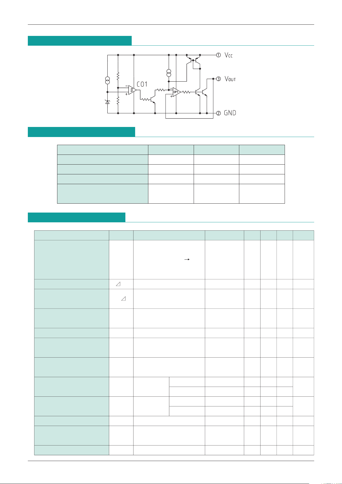
Equivalent Circuit Diagram
Item Symbol Rating Units
Storage temperature T
STG
-
40~+125
°
C
Operating temperature T
OPR
-
20~+75
°
C
Power supply voltage V
CC max.
-
0.3~10 V
Allowable loss Pd
200 (MMP-3A)
mW
300 (TO-92A)
Item Symbol Measurement conditions
Measurement circuit
Min. Typ. Max. Units
4.6~
Detection voltage V
S RL=470Ω VCC=H L 1
VStyp.
1.9
VStyp.
V
-
2% (0.1V +2%
Step
)
Hysteresis voltage V
S RL=470Ω 1 30 50 100 mV
Detection voltage
V
S/ T RL=470Ω 1 ±0.01 %/
°
C
temperature coefficient
Low-level output voltage V
OL
VCC=VS min. -0.05V
1 0.2 0.4 V
R
L=470Ω
Output leakage current I
OH VCC=10.0V 1 0.1 µA
Circuit current while on I
CCL
VCC=VS min. -0.05V
1 3.0 6.0 µA
R
L=∞
Circuit current while off I
CCH
VCC=VS typ. /0.85V
1 2.0 4.0 µA
R
L=∞
"H"transport delay time t
PLH
RL=4.7kΩ 7046~24 2 5 30
µS
C
L=100P 7023~19 2 10 30
"L"transport delay time t
PHL
RL=4.7kΩ 7046~24 2 30 70
µS
C
L=100P 7023~19 2 70 150
Operation limit voltage V
OPL RL=4.7kΩ VOL
<
=
0.4V 1 0.65 0.85 V
Output current while on 1 I
OL1
V
CC=VS min.
-
0.05V
1 8 30 mA
R
L=0Ω
Output current while on 2 I
OL2 Ta=
-
20°C~+75°C15 mA
 Loading...