

MITSMI PST623XS, PST623XW Datasheet
MITSUMI
System Reset PST623
System Reset
Monolithic IC PST623
Outline
This low reset type IC functions in CPU and other logic systems to detect input voltage and reset the system
accurately when power is turned on or interruped.
Features
1. Detection voltage can be set easily (2 external resistors)
2. High percision voltage detection Internal reference voltage 1.25±2%
3. Enables high voltage check (at stage before Reg)
4. Low operating limit voltage 0.65V typ.
5. High output current during ON 10mA min.
6. Low current consumption 40µA typ.
7. Built-in delay circuit (1 external capacitor)
Applications
1. Reset circuits in microcomputers, CPUs and MPUs
2. Logic circuit reset circuits
3. Level detection circuits
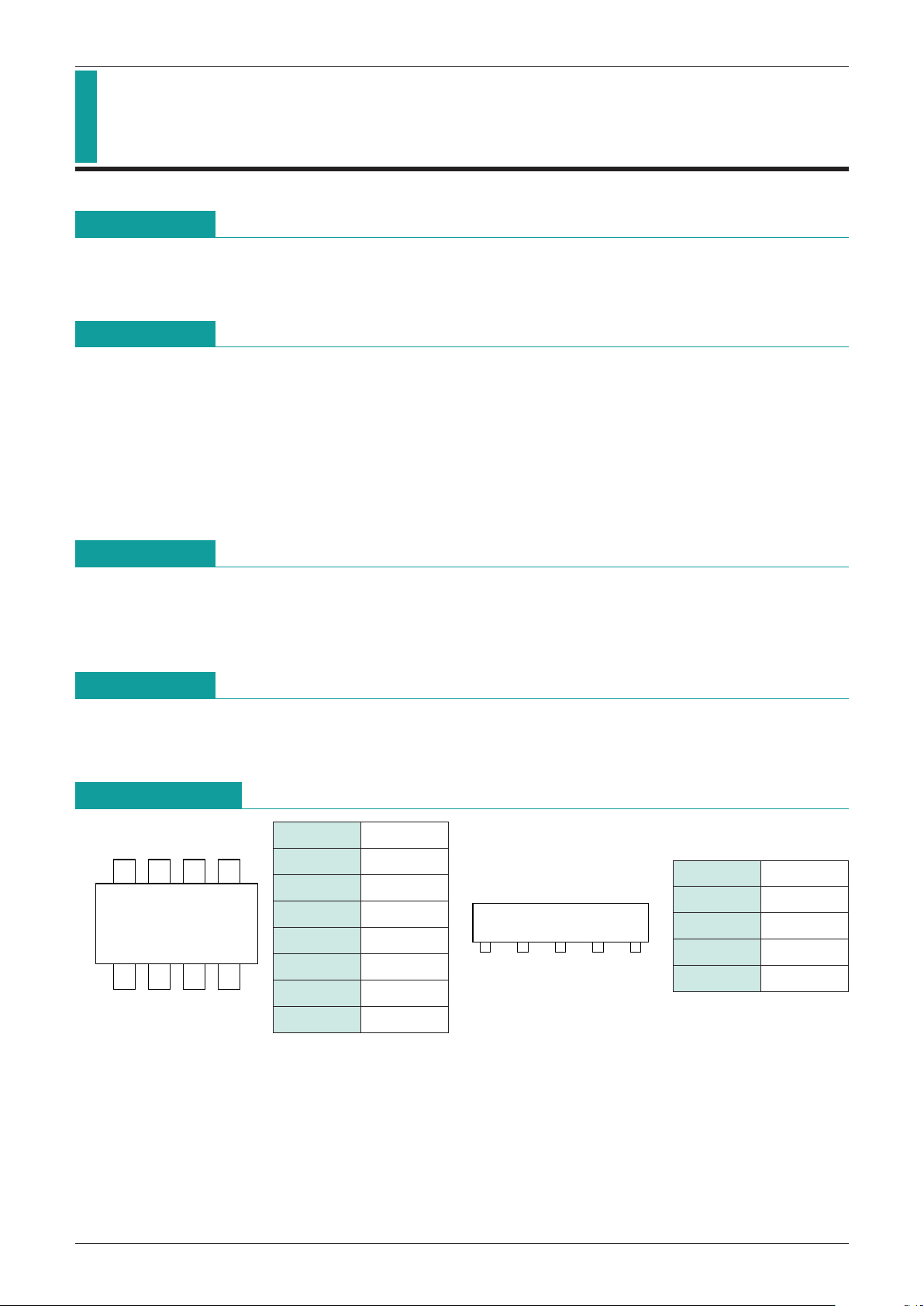
Package
VSOP-8A (PST623XS)
SIP-5A (PST623XW)
Pin Assignment
1432
8765
VSOP-8A
1 VS
2 NC
3 TC
4 GND
5 RESET
6 NC
7 NC
8 V
CC
SIP-5A
12345
1 VCC
2 VS
3 TC
4 GND
5 RESET
MITSUMI
System Reset PST623
Absolute Maximum Ratings
(Ta=25°C)
Item Symbol Rating Units
Storage temperature T
STG
-
40~+125
°
C
Maximum power supply voltage V
CC max. 10 V
Allowable power consumption Pd max. 300 mW
Input pin voltage V
ID
-
0.3~VCC V
Recommended Operating Conditions
Item Symbol Rating Units
Power supply voltage V
CCOP 2.0~10.0 V
Operating temperature T
OPG
-
25~+75
°
C
Electrical Characteristics
(Except where noted otherwise, VCC=5V, Ta=25°C)
Item Symbol Measurement conditions Min. Typ. Max. Units
Detection reference voltage V
S RL=470Ω, VIN=H L 1.225 1.25 1.275 V
Hysteresis voltage V
S RL=470Ω, VIN=L H L 12 25 50 mV
Detection reference voltage
R
L=470Ω, Ta=
-
25~+75°C ±0.01 %/°C
temperature coefficient
L level output voltage V
OL VIN=1.0V, RL=470Ω 0.3 0.45 V
Output leakage current I
OH VIN=1.5V, VOUT=10V ±0.1 µA
Circuit current while on I
CCL VIN=1.0V, RL=∞ 50 90 µA
Circuit current while off I
CCH VIN=1.5V, RL=∞ 42 70 µA
"H" transport delay time tpLH R
L=4.7kΩ, Cd=0.047uF 110 mS
"L" transport delay time tpHL R
L=4.7kΩ, Cd=0.047uF 15 µS
R
L=4.7kΩ, VOL
<
=
0.4V
Operation limit voltage V
OPL Minimum power supply voltage for 0.65 0.85 V
which output can maintain Lo.
Output current while on I
OL VIN=1.0V, RL=0 10 mA
Delay time setting comparator
Vtsh R
L=470Ω, VTC=L H 1.25 1.4 1.55 V
Threshold level
Capacitor charging current ITC VIN=1.5V, VTC=0.2V 0.39 0.60 0.81 µA
Vs input current I
IN VIN=1.35V 40 nA
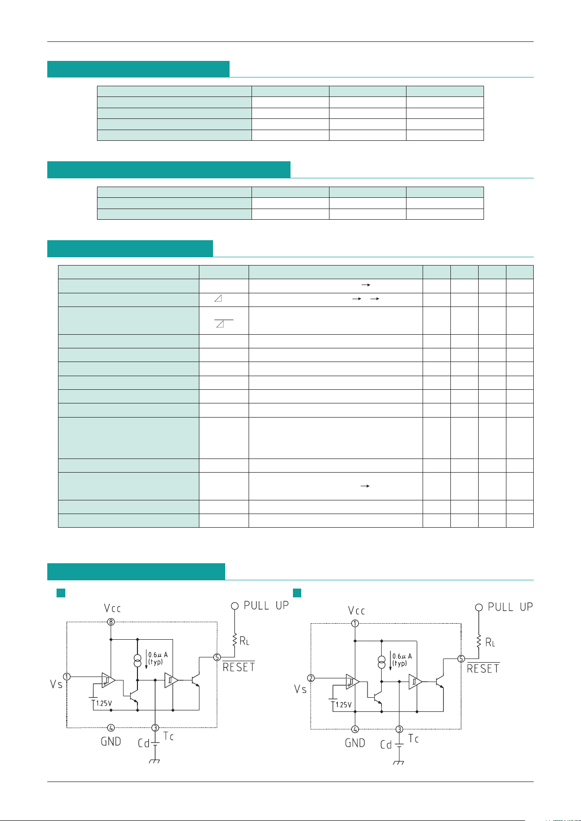
Equivalent Circuit Diagram
Vs
T
VSOP-8A SIP-5A
 Loading...