

MITSMI MM1501, MM1502, MM1503, MM1510, MM1511 Datasheet
...
MITSUMI
Video Switch · 75Ω driver · Y/C mix MM1501
Video Switch · 75Ω driver · Y/C mix
Monolithic IC MM1501 Series
Outline
This IC extends the series of ICs for video/audio signal switching, with a 2-input 1-output single video switch,
video signal/chroma signal 75Ω driver, and Y/C mixing circuit in one small package (SOT-26).
Features
(1) Low power consumption achieved.
(2) Low power supply voltage realized.
(3) Frequency bandwidth without 75Ω driver: 10MHz with 75Ω driver: 7MHz
(4) Cross talk 70dB When 4.43MHz
(5) With SAG measures pin (75Ω driver and Y/C mix driver)
Package
SOT-26A (with 75Ω driver)
SOT-26B (without 75Ω driver)
Applications
(1) TV
(2) VTR
(3) Video camera
(4) Digital still camera
(5) Other visual equipment
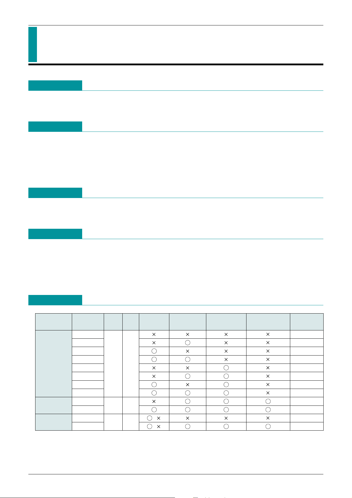
Line-up
Functions
Switch
Driver
Y/C mix
Model Name
MM1501 4.5~13.0V
MM1502 4.5~13.0V
MM1503 4.5~13.0V
MM1504
MM1505 4.5~13.0V
MM1506 4.5~13.0V
MM1507 4.5~13.0V
MM1508 4.5~13.0V
MM1509
MM1510 4.5~13.0V
MM1511
MM1512 / 4.5~13.0V
Input
Output
21
11
11
Clamp 6dB amp 75Ω driver
/ 4.5~13.0V
SAG measures pin
Power supply
voltage
4.5~13.0V
4.5~13.0V
MITSUMI
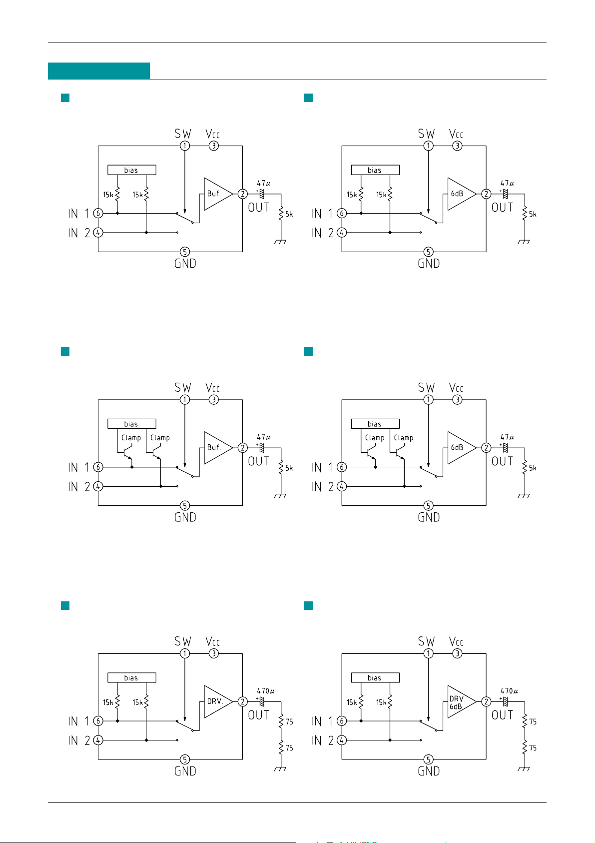
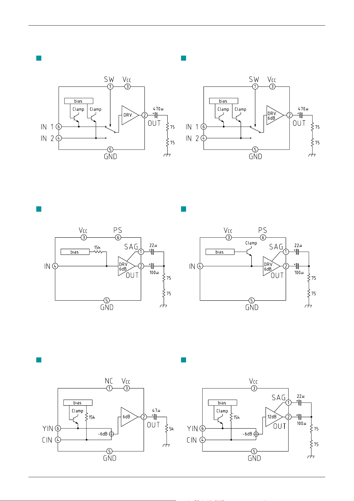
Block Diagram
MM1501 MM1502
Video Switch · 75Ω driver · Y/C mix MM1501
MM1503 MM1504
MM1505 MM1506
MITSUMI
MM1507 MM1508
Video Switch · 75Ω driver · Y/C mix MM1501
MM1509 MM1510
MM1511 MM1512
MITSUMI
Video Switch · 75Ω driver · Y/C mix MM1501
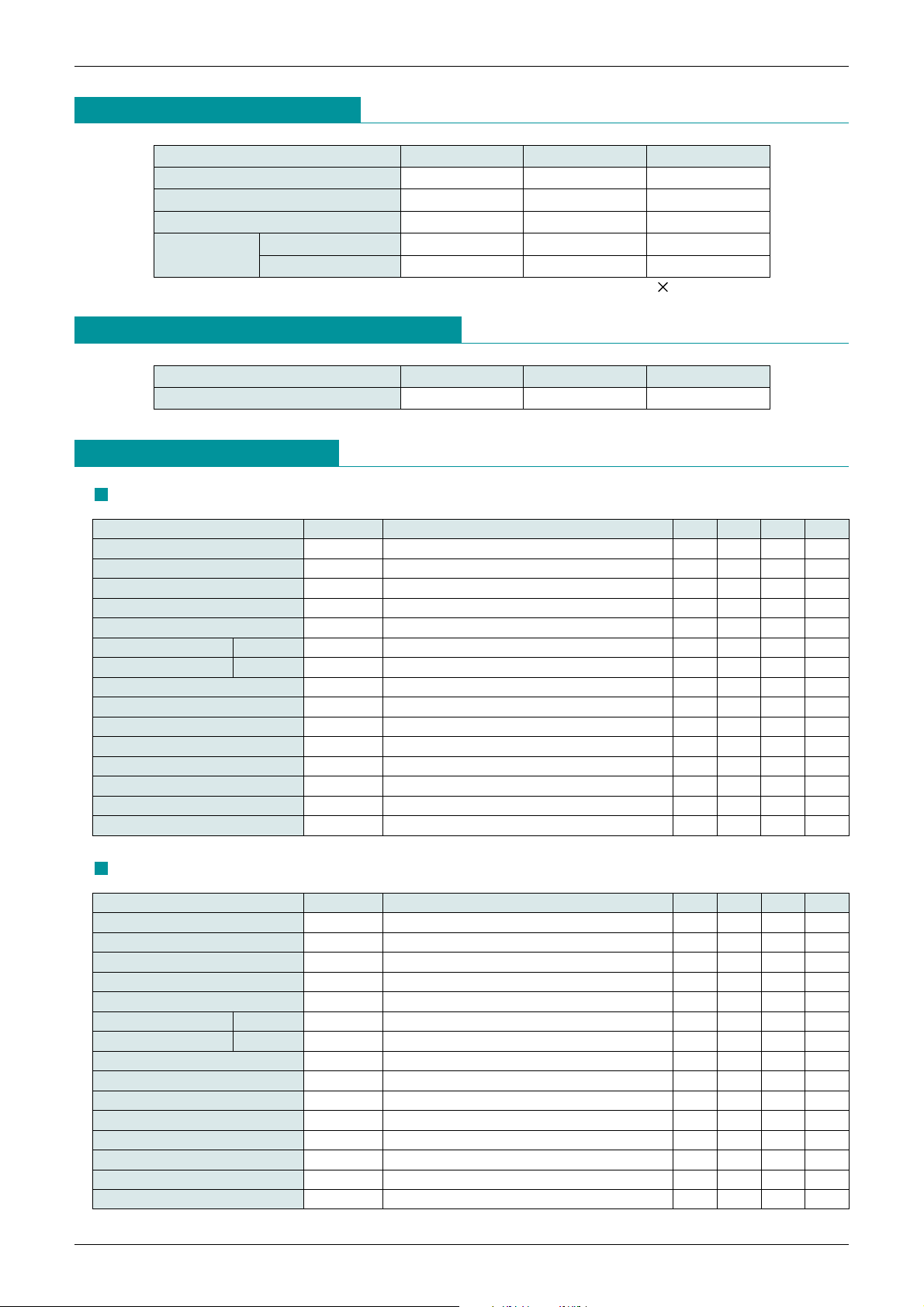
Absolute Maximum Ratings
(Ta=25°C)
Item Symbol Rating Unit
Storage temperature T
Operating temperature T
Power supply voltage V
Allowable loss
When alone Pd 200 mW
When mounted on board
STG
OPR
CC 15 V
-
40~+125 °C
-
30~+75 °C
Pd 350 (*)mW
Board size 100mm 100mm t=1.6
*
Recommended Operating Conditions
Item Symbol Rating Unit
Power supply voltage V
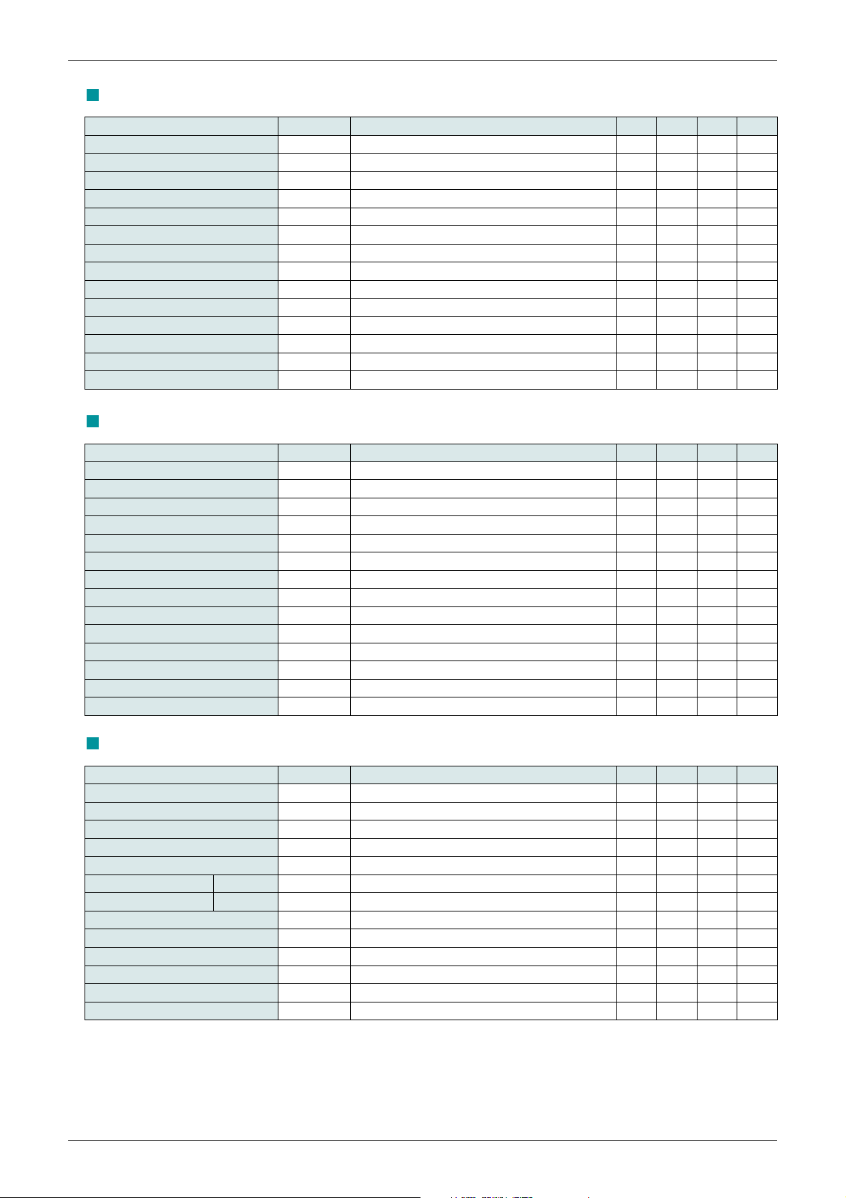
Electrical Characteristics
(Except where noted otherwise, Ta=25°C, VCC=5V)
MM1501
Item Symbol Measurement conditions Min. Typ. Max. Unit
Consumption current I
Input pin voltage V
Output pin voltage V
Voltage gain G
Frequency characteristic fc Refer to measurement procedures
Differential gain V
Differential phase V
CC=9V DG Refer to measurement procedures
CC=9V DP Refer to measurement procedures
Total harmonic distortion ratio
Output dynamic range V
Output offset voltage V
Cross talk C
SW input voltage H V
SW input voltage L V
Input impedance Zi 15 kΩ
Output impedance Zo 75 Ω
CC Refer to measurement procedures 3.7 4.8 mA
IN No-signal, no-load 2.70 2.90 3.10 V
OUT No-signal, no-load 2.15 V
V Refer to measurement procedures
THD Refer to measurement procedures 0.03 0.3 %
D Refer to measurement procedures 3.5 3.8 V
OFF Refer to measurement procedures ±15 mV
T Refer to measurement procedures
IH Refer to measurement procedures 2.1 V
IL Refer to measurement procedures 0.7 V
CC 4.5~13 V
-
0.5 0 +0.5 dB
-
10+1dB
-
30+3%
-
3 0 +3 deg
-
70-60 dB
MM1502
Item Symbol Measurement conditions Min. Typ. Max. Unit
Consumption current I
Input pin voltage V
Output pin voltage V
Voltage gain G
Frequency characteristic fc Refer to measurement procedures
Differential gain V
Differential phase V
CC=9V DG Refer to measurement procedures
CC=9V DP Refer to measurement procedures
Total harmonic distortion ratio
Output dynamic range V
Output offset voltage V
Cross talk C
SW input voltage H V
Sw input voltage L V
Input impedance Zi 15 kΩ
Output impedance Zo 12 Ω
CC Refer to measurement procedures 4.7 6.1 mA
IN No-signal, no-load 1.70 1.90 2.10 V
OUT No-signal, no-load 2.10 V
V Refer to measurement procedures 5.5 6.0 6.5 dB
-
10+1dB
-
30+3%
-
3 0 +3 deg
THD Refer to measurement procedures 0.03 0.3 %
D Refer to measurement procedures 3.5 3.8 V
OFF Refer to measurement procedures ±30 mV
T Refer to measurement procedures
IH Refer to measurement procedures 2.1 V
IL Refer to measurement procedures 0.7 V
-
70-60 dB
MITSUMI
Video Switch · 75Ω driver · Y/C mix MM1501
MM1503
Item Symbol Measurement conditions Min. Typ. Max. Unit
Consumption current I
Input pin voltage V
Output pin voltage V
Voltage gain G
CC Refer to measurement procedures 3.3 4.3 mA
IN No-signal, no-load 1.80 2.00 2.20 V
OUT No-signal, no-load 1.25 V
V Refer to measurement procedures
Frequency characteristic fc Refer to measurement procedures
Differential gain DG Refer to measurement procedures
Differential phase DP Refer to measurement procedures
Total harmonic distortion ratio
Output dynamic range V
Output offset voltage V
Cross talk C
SW input voltage H V
SW input voltage L V
THD Refer to measurement procedures 0.03 0.3 %
D Refer to measurement procedures 2.6 2.9 V
OFF Refer to measurement procedures ±15 mV
T Refer to measurement procedures
IH Refer to measurement procedures 2.1 V
IL Refer to measurement procedures 0.7 V
Input impedance Zo 75 Ω
MM1504
Item Symbol Measurement conditions Min. Typ. Max. Unit
Consumption current I
Input pin voltage V
Output pin voltage V
Voltage gain G
Frequency characteristic fc Refer to measurement procedures
Differential gain DG Refer to measurement procedures
Differential phase DP Refer to measurement procedures
Total harmonic distortion ratio
Output dynamic range V
Output offset voltage V
Cross talk C
SW input voltage H V
SW input voltage L V
Input impedance Zo 12 Ω
CC Refer to measurement procedures 4.4 5.7 mA
IN No-signal, no-load 1.20 1.40 1.60 V
OUT No-signal, no-load 1.25 V
V Refer to measurement procedures 5.5 6.0 6.5 dB
THD Refer to measurement procedures 0.03 0.3 %
D Refer to measurement procedures 2.6 2.9 V
OFF Refer to measurement procedures ±30 mV
T Refer to measurement procedures
IH Refer to measurement procedures 2.1 V
IL Refer to measurement procedures 0.7 V
-
0.5 0 +0.5 dB
-
10+1dB
-
30+3%
-
3 0 +3 deg
-
70-60 dB
-
10+1dB
-
30+3%
-
3 0 +3 deg
-
70-60 dB
MM1505
Item Symbol Measurement conditions Min. Typ. Max. Unit
Consumption current I
Input pin voltage V
Output pin voltage V
Voltage gain G
Frequency characteristic fc Refer to measurement procedures
Differential gain V
Differential phase V
CC=9V DG Refer to measurement procedures
CC=9V DP Refer to measurement procedures
Output dynamic range V
Output offset voltage V
Cross talk C
SW input voltage H V
SW input voltage L V
Input impedance Zi 15 kΩ
CC Refer to measurement procedures 6.5 8.5 mA
IN No-signal, no-load 2.35 2.55 2.75 V
OUT No-signal, no-load 2.55 V
V Refer to measurement procedures
D Refer to measurement procedures 2.6 3.0 V
OFF Refer to measurement procedures ±15 mV
T Refer to measurement procedures
IH Refer to measurement procedures 2.1 V
IL Refer to measurement procedures 0.7 V
-
0.5 0.0 0.5 dB
-
10+1dB
-
30+3%
-
3 0 +3 deg
-
70-60 dB
 Loading...