

MITSMI MM1475 Datasheet
MITSUMI
Lithium Ion Battery Charging Control (microcomputer-controlled type) MM1475
Lithium Ion Battery Charging Control (microcomputer-controlled type)
Monolithic IC MM1475
Outline
This IC was developed as part of the MM1433 series of lithium ion battery charging ICs. MM1433 is a
charging IC with charging functions (quick charge, pre-charge) and all battery protection functions, while this
IC has charging control functions and some safety functions, with battery protection functions being
controlled by the external MPU.
Features
(1) Rated current, rated voltage charging
(2) Charging precision ± 30mV/cell (Ta = 0°C ~ +50°C)
(3) Pre-charge function and pre-charging over timer
(4) Input overvoltage, adaptor detection functions
(5) Battery temperature detection function
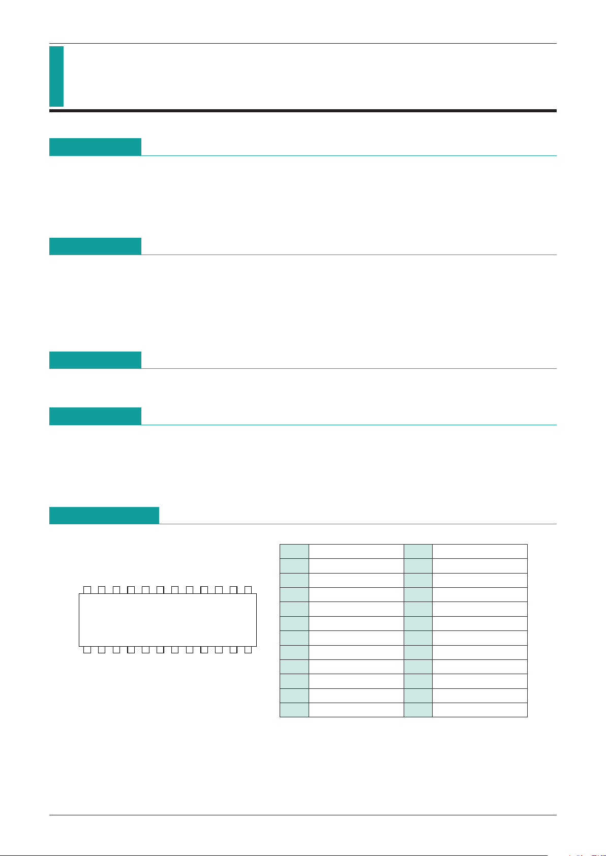
Package
TSOP-24A
Applications
Applications
(1) Mobile telephones
(2) PDA
(3) Movies
(4) Other equipment using lithium ion batteries
Pin Assignment
136924587101211
24 20 1723 21 19 18 1622 131415
TSOP-24A
1 SW1 13 BAT
2 SW2 14 CS
-
3 TP1 15 CS+
4 NC 16 CFB
5 VREF 17 CNT
6 GND1 18 V
CC
7 GND2 19 VOUT2
8 NC 20 V
OUT1
9 ADJ1 21 VDET
-
TD
10 CDO 22 NC
11 T
OUT 23 OSC OUT
12 TDET 24 OSC FB
-
MITSUMI
Lithium Ion Battery Charging Control (microcomputer-controlled type) MM1475
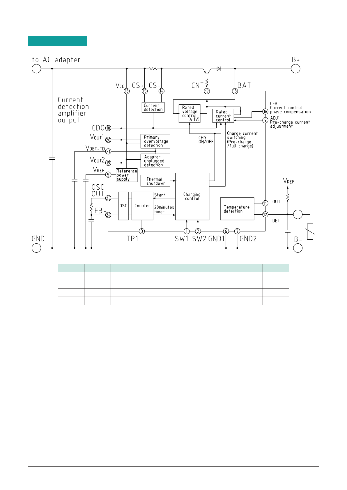
Block Diagram
SW1 SW2 Charging Current limit Timer
L H OFF OFF
H H ON Controlled by this IC (Current limit 2: 25mV) ON
LLON
Controlled by adaptor (Current limit 1: 450mV)
OFF
HLON
Controlled by adaptor (Current limit 1: 450mV)
OFF
MITSUMI
Lithium Ion Battery Charging Control (microcomputer-controlled type) MM1475
Pin Description
Pin No. Pin name I
/O Function
Function
1 SW1 Input
Charge control switching pin.
Switches charging ON/OFF and switches charging current by combinations
of SW1 and SW2 high and low.
2 SW2 Input
3 TP1
Input/output
Test pin 1.
Pre-charge timer test pin.
Inverts during counting (from the middle stage of the several-staged FF) and
outputs on TP1 for monitoring.
Also inverts TP1 output signal again inside the IC and inputs to the next stage FF.
(Timer setting done by binary counter.)
Reference power supply output pin.
Outputs 1.2V typ. reference voltage.
5 VREF Output
6 GND1 Input
Ground pin.
Ground pin.
7 GND2 Input
9 ADJ1 Input
Pre-charge current adjustment pin.
Pin voltage is set at 100mV typ.. Pre-charge current can be changed by
adjusting pin voltage with an external resistor.
Pre-charge current is controlled by comparing ADJ1 pin voltage and the 12dB
voltage drop value between CS + and CS
-
.
10 CDO Output
Current detection output pin.
Outputs voltage difference of 18dB between CS+ and CS
-
.
11 TOUT Output
Temperature detection output pin.
Normal temperature: Output Tr OFF
When high temperature is detected: Output Tr ON
12 TDET Input
Temperature detection input pin.
Be sure to apply the potential obtained by resistance dividing, from reference
voltage, with an external resistor and thermistor.
13 BAT Input
Battery voltage input pin.
Detects battery voltage and controls charging.
16 CFB Input
Rated current control phase compensation pin.
Oscillation is improved by connecting an external capacitor (around 100pF)
between CFB and CNT to perform phase compensation.
14 CS
-
Input
15 CS+ Input
Current detection pin.
Detects current by voltage drop at external resistor between (CS+) and (CS
-
)
and controls charging current.
17 CNT Output
Charging control output pin.
Controls base of external PNP-Tr for rated current rated voltage charging.
18 VCC Input
Power supply input pin.
19 VOUT2 Output
Adapter unplugged detection output pin.
V
CC low voltage input: Output Tr OFF
V
CC recommended operating voltage: Output Tr ON
20 VOUT1 Output
Overvoltage detection output pin.
V
CC overvoltage input: Output Tr OFF
V
CC recommended operating voltage: Output Tr ON
21 VDET-TD Input
Overvoltage detection delay time setting pin.
Delay time is set by connecting an external capacitor.
23 OSC OUT Output
Oscillator output pin.
Timer setting time changes according to oscillation frequency. Oscillation
frequency is determined by the external resistor (connected between OSC
OUT and OSC FB) and capacitor (connected between OSC FB and GND).
24 OSC FB
-
Input
Oscillator inverted input pin.
MITSUMI
Lithium Ion Battery Charging Control (microcomputer-controlled type) MM1475
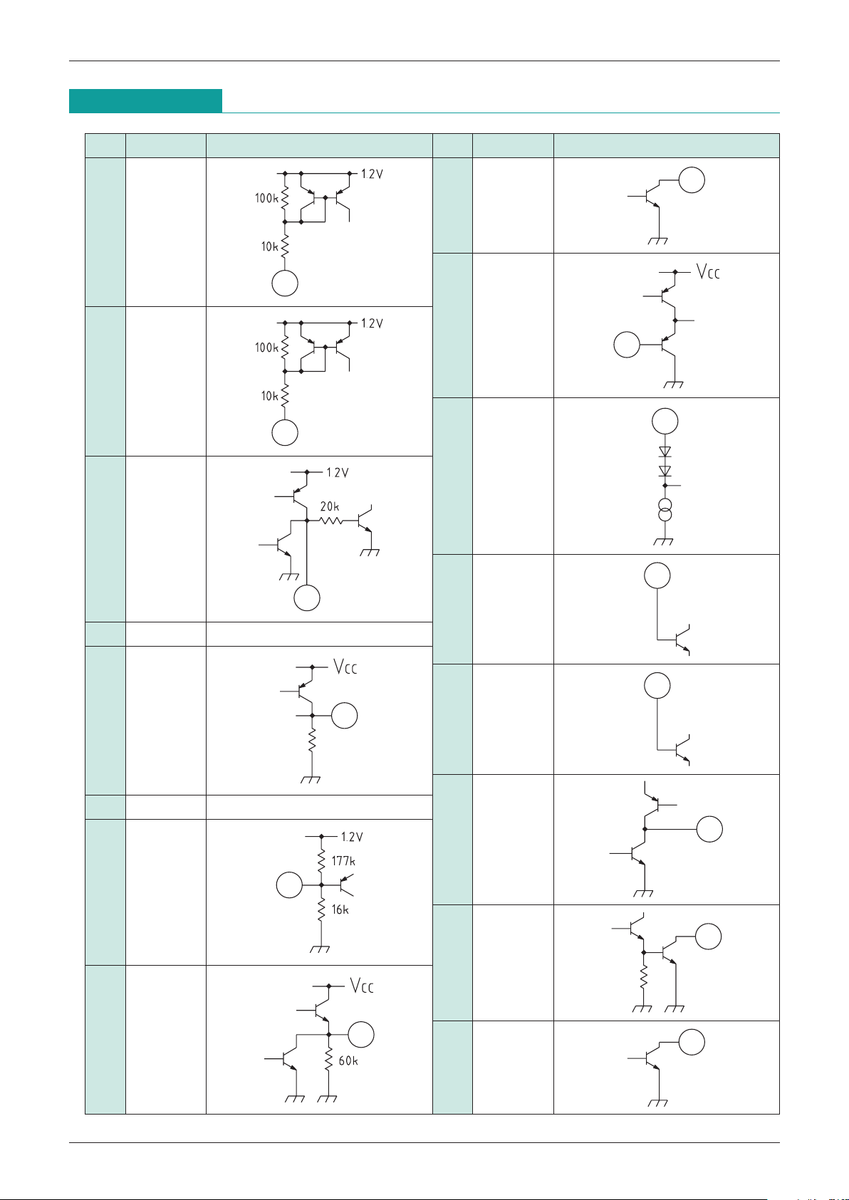
Pin Description
The following valaeis typical
Pin No.
Pin name
Internal equivalent circuit diagram
Pin No.
Pin name
Internal equivalent circuit diagram
1 SW1
12 TDET
13 BAT
2 SW2
3 TP1
5 VREF
4 NC
8 NC
9 ADJ1
10 CDO
11 TOUT
14 CS
-
15 CS +
16 CFB
17 CNT
19 VOUT2
 Loading...