

MITSMI MM1469XH Datasheet

MITSUMI
4-ch BTL Motor Driver for CD Players
4-ch BTL Motor Driver for CD Players
Monolithic IC MM1469
Outline
This IC is a 4-ch BTL driver developed for driving CD player motors and actuators.
With built-in 3.3V (MM1469PH) or 5.0V (MM1469XH) regulator and general-purpose op amp, it supports a
variety of applications.
Features
(1) External resistor allows gain adjustment.
(2) Few external parts.
(3) Built-in 3.3V or 5.0V regulator. (Requires external PNP Tr.)
(4) Built-in general-purpose op amp.
(5) Built-in thermal shutdown circuit.
Package
HSOP-28
Applications
(1) CD radio cassette recorder
(2) VCD
Block diagram
(MM1469XH)
10kΩ
10kΩ
10kΩ
(3.3kΩ)
10kΩ
10kΩ
50kΩ
50kΩ
10kΩ
D.BUFD.BUF
D.BUF D.BUF D.BUF
V
CC VCC
D.BUF D.BUF
D.BUF
DRIVER MUTE
1
28 27 26 25 24 23 22
21 20 19 18 17 16 15
2 3 4 5 6 7
8 9 10 11 12 13 14
T.S.D
Level shift
Level shift
Level shift
Level shift
T. S. D : Thermal Shut Down
D. BUF : Driver Buffer
13kΩ
13kΩ
1kΩ
1kΩ
1kΩ
1kΩ
13kΩ 13kΩ
note Constane in parenehesis is regulator output voltage 3.3V(MM1469PH).
MITSUMI
4-ch BTL Motor Driver for CD Players
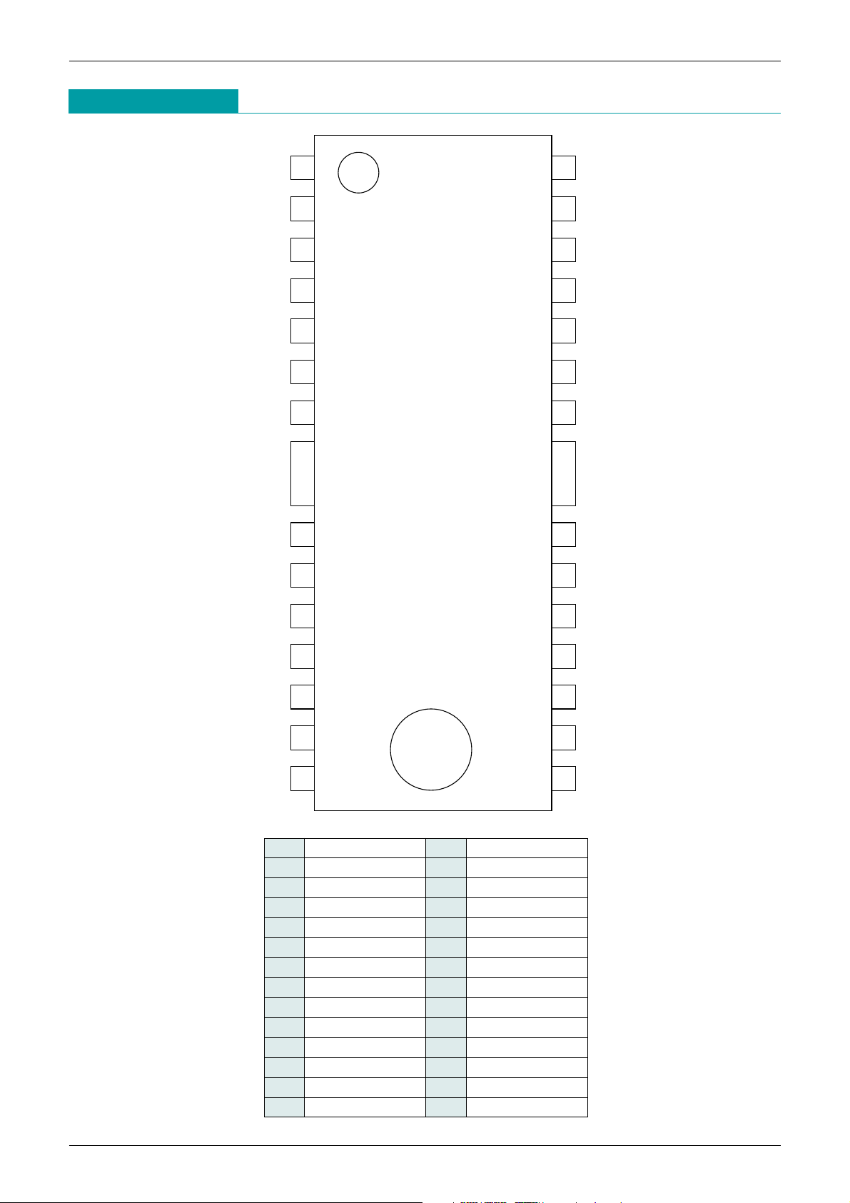
Pin configuration
1
3
7
6
2
4
5
8
13
11
14
12
9
10
28
26
22
23
27
25
24
21
16
18
15
17
20
19
ch1 OUT-A
ch1 OUT
-
B
ch1 IN
-
A
ch1 IN
-
B
Tr
-
B
V
REG
-
OUT
MUTE
GND
ch2 IN
-
B
ch2 IN
-
A
ch2 OUT
-
B
ch2 OUT
-
A
SUBGND
OP OUT
SUBGND
ch4 OUT
-
A
ch4 OUT
-
B
ch4 IN
-
A
ch4 IN
-
B
BIAS
-
IN
V
CC
VCC
ch3 IN-B
ch3 IN
-
A
ch3 OUT
-
B
ch3 OUT
-
A
OP IN(+)
OP IN(–)
1 ch1 OUT–A 15 OP IN(–)
2 ch1 OUT–B 16 OP IN(+)
3 ch1 IN–A 17 ch3 OUT–A
4 ch1 IN–B 18 ch3 OUT–B
5 Tr–B 19 ch3 IN–A
6 V
REG– OUT 20 ch3 IN–B
7 MUTE 21 V
CC
8 GND 22 VCC
9 ch2 IN–B 23 BIAS–IN
10 ch2 IN–A 24 ch4 IN–B
11 ch2 OUT–B 25 ch4 IN–A
12 ch2 OUT–A 26 ch4 OUT–B
13 SUBGND 27 ch4 OUT–A
14 OP OUT 28 SUBGND

MITSUMI
4-ch BTL Motor Driver for CD Players
Pin No. Pin Name Function Internal equivalent circuit
1 ch1–OUT A
12 ch2–OUT A
17 ch3–OUT A
27 ch4–OUT A
Driver ch1 negative output
Driver ch2 negative output
Driver ch3 negative output
Driver ch4 negative output
2
1
12kΩ 12kΩ
600
Ω
600
Ω
V
CC
12
17
27
11
18
26
2 ch1–OUT B
11 ch2–OUT B
18 ch3–OUT B
26 ch4–OUT B
Driver ch1 positive output
Driver ch2 positive output
Driver ch3 positive output
Driver ch4 positive output
3 ch1–IN A
10 ch2–IN A
19 ch3–IN A
25 ch4–IN A
Driver ch1 input
Driver ch2 input
Driver ch3 input
Driver ch4 input
4
3
10kΩ10kΩ
10kΩ
10µA
V
CC
2.5V
10
19
25
9
20
24
4 ch1–IN B
9 ch2–IN B
20 ch3–IN B
24 ch4–IN B
Driver ch1 input, gain adjustment pin
Driver ch2 input, gain adjustment pin
Driver ch3 input, gain adjustment pin
Driver ch4 input, gain adjustment pin
Terminal explanations
5 Tr–B Connect to external transistor base
5
15kΩ 40kΩ
6kΩ
V
CC
6 VREG –OUT Constant voltage output, connects to
external transistor collector
6
10kΩ
10kΩ
3kΩ 3kΩ
V
CC
10µA
2.5V
 Loading...