

MITSMI MM1394 Datasheet

MITSUMI
MITSUMI
NTSC/PAL Encoder MM1394
NTSC/PAL Encoder
Monolithic IC MM1394
Outline
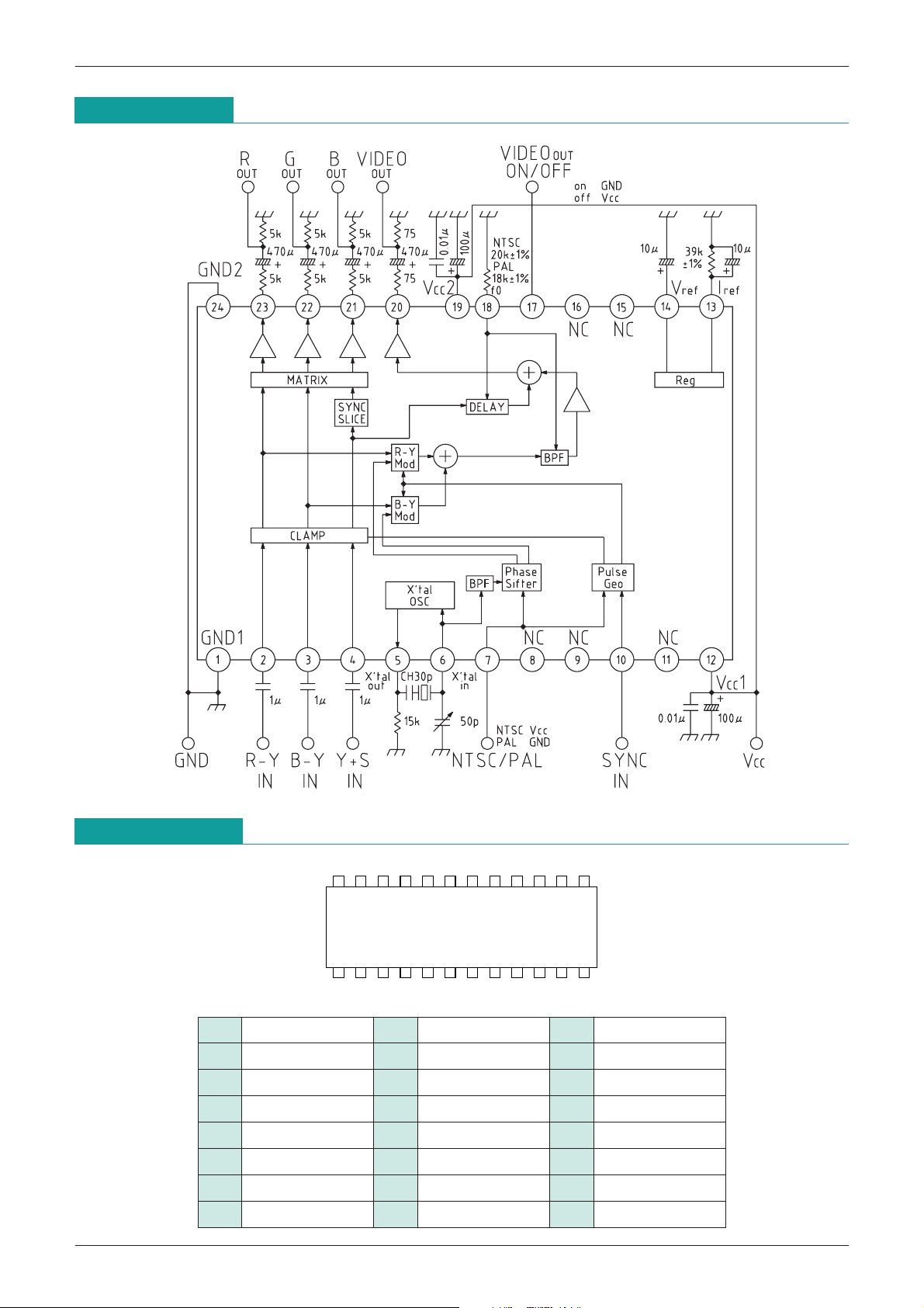
This is an encoder IC that converts luminance signal Y, color difference signals R-Y and B-Y to composite
video signals and RGB signals.
Features
1. Operates on 5V single power supply
2. Low power consumption (265mW : video output ON)
(165mW : video output OFF)
3. Supports both NTSC and PAL formats
4. Built-in 75Ω drive output (RGB output, composite output)
5. BPF and DELAY filters built-in
6. Built-in oscillator for subcarrier
7. Built-in video output ON/OFF circuit
Package
SOP-24
Applications
1. Game equipment
2. Digital cameras
3. Other video equipment
MITSUMI
SOP-24
136924587101211
24 20 1723 21 19 18 1622 131415
Block Diagram
NTSC/PAL Encoder MM1394
Pin Assignment
1 GND1 9 NC 17
2 R-Y IN 10 SYNC IN 18 f0
3 B
4 Y+S
5 X' tal OUT 13 Iref 21 B OUT
6 X' tal IN 14 Vref 22 G OUT
7 NTSC/PAL 15 NC 23 R OUT
8 NC 16 NC 24 GND2
-
Y IN 11 NC 19 VCC2
IN 12 VCC1 20 VIDEO OUT
VIDEO
OUT
ON/OFF
MITSUMI
MITSUMI
NTSC/PAL Encoder MM1394
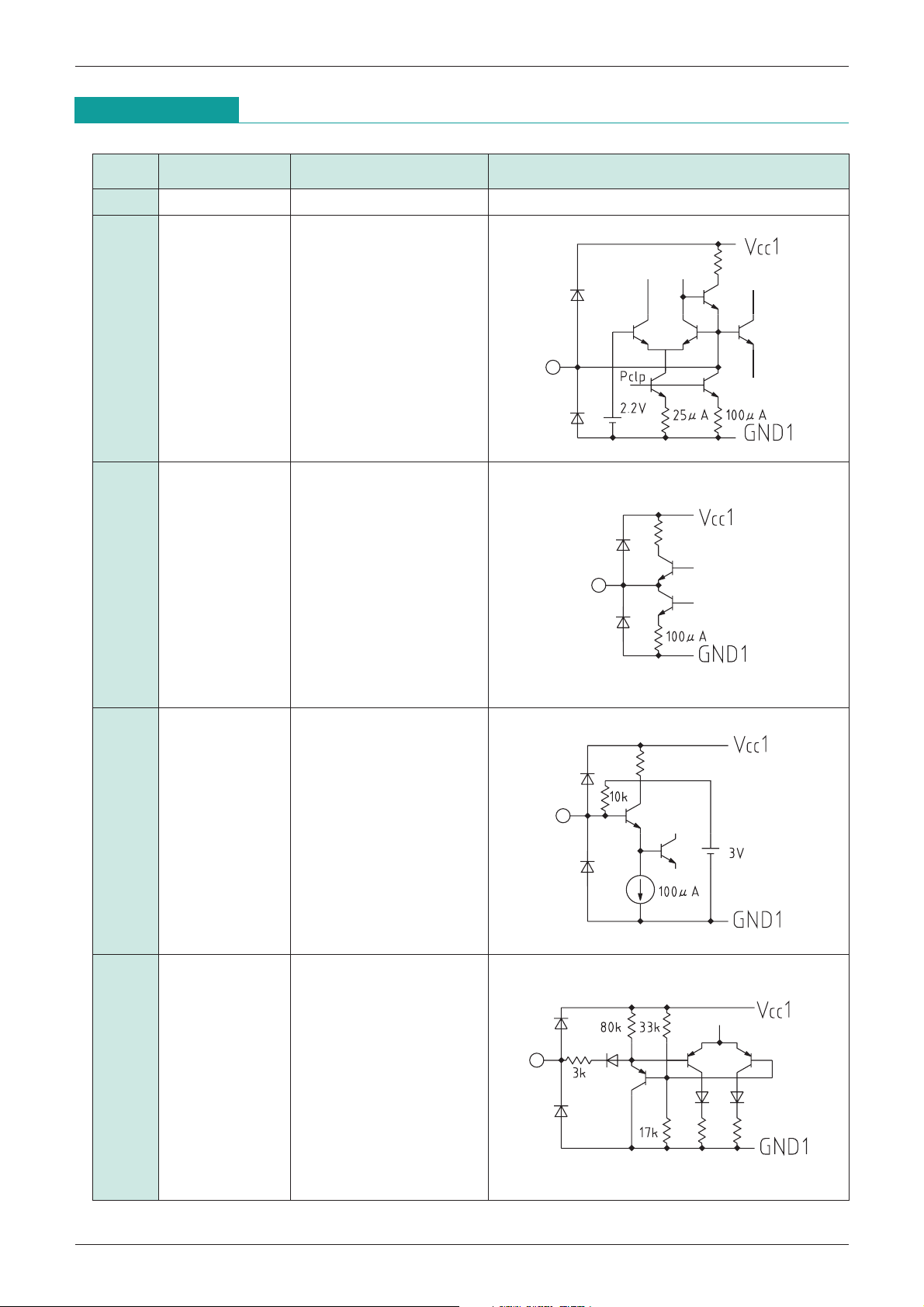
Pin Description
Pin no. Pin name Function Internal equivalent circuit diagram
1 GND1
2 R-YIN Input pins.
3 B
4 Y+S
-
YIN Maximum input voltage :
IN R
-
Y 1.00VP
B-Y 1.27VP
Y+S 1.00VP
-
P
-
P
-
P
(SYNC is 0.286VP
-
P)
DC level for clamp is 2.2V.
5 X' tal OUT Oscillator circuit output pin
6 X' tal in Subcarrier input pin
Input a 0.4~1.0V
P-P
sine wave.
7 NTSC/PAL Mode setting pin
NTSC : V
CC
PAL : PAL

MITSUMI
MITSUMI
NTSC/PAL Encoder MM1394
Pin no. Pin name Function Internal equivalent circuit diagram
8
NC OPEN
9
10 SYNC IN Composite sync signal
input pin
11 NC OPEN
12 VCC1
13 Iref
Determines internal
reference current.
Connect a 47kΩ resistor
between this pin and GND.
14 Vref Internal reference voltage
pin
Reference voltage : 4V
Connect a 10µF capacitor
between this pin and GND.
15
16
NC OPEN
 Loading...