

MITSMI MM1383XD, MM1381XD, MM1382XD Datasheet
MITSUMI
RGB Video Amplifier with OSD Input MM1381, 1382, 1383
RGB Video Amplifier with OSD Input
Monolithic IC MM1381, 1382, 1383
Outline
MM1381XD, MM1382XD and MM1383XD are wideband RGB video amplifiers with OSD input, developed for
use in monitors. The main differences between them are video amp bandwidth and output rise time, and
output fall time.
Features
1. Built-in wideband video amp 110MHz @ -3dB (4VP
-
P output)
2. OSD input has TTL interface bandwidth 50MHz
3. Output voltage less than 0.1V for blanking
4. High-speed switching between VIDEO/OSD
5. Each channel has an independent drive pin for color balance adjustment
6. Built-in high impedance DC contrast control, 0~4V (> 40dB range)
7. Built-in high impedance DC drive control, 0~4V (±3dB range)
8. Built-in high impedance DC OSD contrast control, 0~4V (> 40dB range)
9. 7V
P-P output swing (band slightly attenuated)
10Output can drive hybrid or discrete CRT drivers directly
Package
DIP-28C (MM1381XD, MM1382XD, MM1383XD)
Applications
1. High resolution RGB CRT monitors with OSD function
2. AGC amps for video
3. Gain and DC offset control
4. LCD or CCD system interface amp
Model MM1381 MM1382 MM1383
Video amp band 85MHz 110MHz 140MHz
Output rise time 3.5nS 3.0nS 2.3nS
Output fall time 4.5nS 4.0nS 3.3nS
MM1382XD is described here as the representative model.
MM1382 is a wideband video amp system with OSD input, developed for use in high resolution RGB
monitors. MM1382 has three matched video amps with a blanking function. All DC control input is high
impedance, and the operating range is set for easy interface with serial bus control systems, at 0~4V. The
OSD section has three TTL inputs and DC contrast control. OSD signals have TTL input interface, and these
signals are made internally so that OSD input low level and video black level are the same. OSD display color
balance follows video signal color balance control adjustment. In addition, MM1382 has a built-in spot-killer
circuit that protects the CRT when monitor power is turned off.

MITSUMI
RGB Video Amplifier with OSD Input MM1381, 1382, 1383
Block Diagram
MITSUMI
RGB Video Amplifier with OSD Input MM1381, 1382, 1383
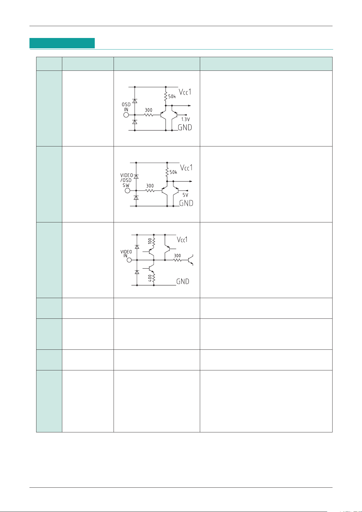
Pin Description
Pin no. Pin name
Internal equivalent circuit diagram
Pin Description
1 R OSD IN
2 G OSD IN
3 B OSD IN
These inputs accept standard TTL input. Each
color is either completely ON (logic high) or
completely OFF (logic low). Connect unused
pins to ground with a 47kΩ resistor.
4 VIDEO/OSD
SWITCH
This input accepts standard TTL input.
H : OSD, L : VIDEO
Connect OSD to ground with a 47kΩ resistor
when not in use.
5 R VIDEO IN
8 G VIDEO IN
11 B VIDEO IN
Video inputs.
These inputs must be AC coupled using a
capacitor of at least 1µF. The ideal capacitance
is 10 (F. DC playback is done with these
inputs. Also, serial resistor of approximately
33Ω must be used.
6 VCC1
9
Power supply pin (except for output stage).
7 GND
10
21
GND pins.
The GND pins are all connected internally, and
must be connected on the board as well.
12 VREF
Used for internal reference additional filter
capacitor. Voltage of this pin is 2.0V.
13
VIDEO CONTRAST
14
OSD CONTRAST
26 B DRIVE
27 G DRIVE
28 R DRIVE
Contrast control pin :
4V no attenuation
0V attenuation over 60dB
Drive control pin :
4V no attenuation
0V 12dB attenuation
 Loading...