

MITSMI MM1365 Datasheet

MITSUMI
1432
8567
VSOP-8
Step-Up IC For EL Backlights MM1365
Step-Up IC For EL Backlights
Monolithic IC MM1365
Outline
This is a step-up IC developed for use in EL backlights.
Because of their ability to light the entire panel uniformly, EL backlights are gradually becoming more
widespread compared with LEDs.
In particular, recently there has been a strong tendency toward smaller sizes and lighter weights, and more
manufacturers are adopting ICs in place of transformers to step up voltages.
This IC was designed to meet these market needs.
Features
1. Low-voltage driving possible VIN=0.95V min.
2. Brightness can be adjusted The brightness can be adjusted by changing the oscillation
frequency through the externally mounted capacitance
3. Can be driven using a small coil Coil inductance of about 820µH required
4. On/off control possible Current consumption while off=10µA or less
Package
VSOP-8
Applications
1. Pagers
2. Portable phones, PHS
3. Wristwatches
4. Display components of remote-controlled minidiscs, CD players, headphone stereos, other equipment
Pin Assignment
1 GND GND
2 N.C
3 CT1 For setting discharge frequency
4 CT2 For setting charging frequency
5
6 V
Power supply
H to turn on, L to turn off
switch
CC Power supply pin
7 O2
Charging frequency setting; drives
external transistor
Discharge frequency setting; drives
8 O1
external transistor
MITSUMI
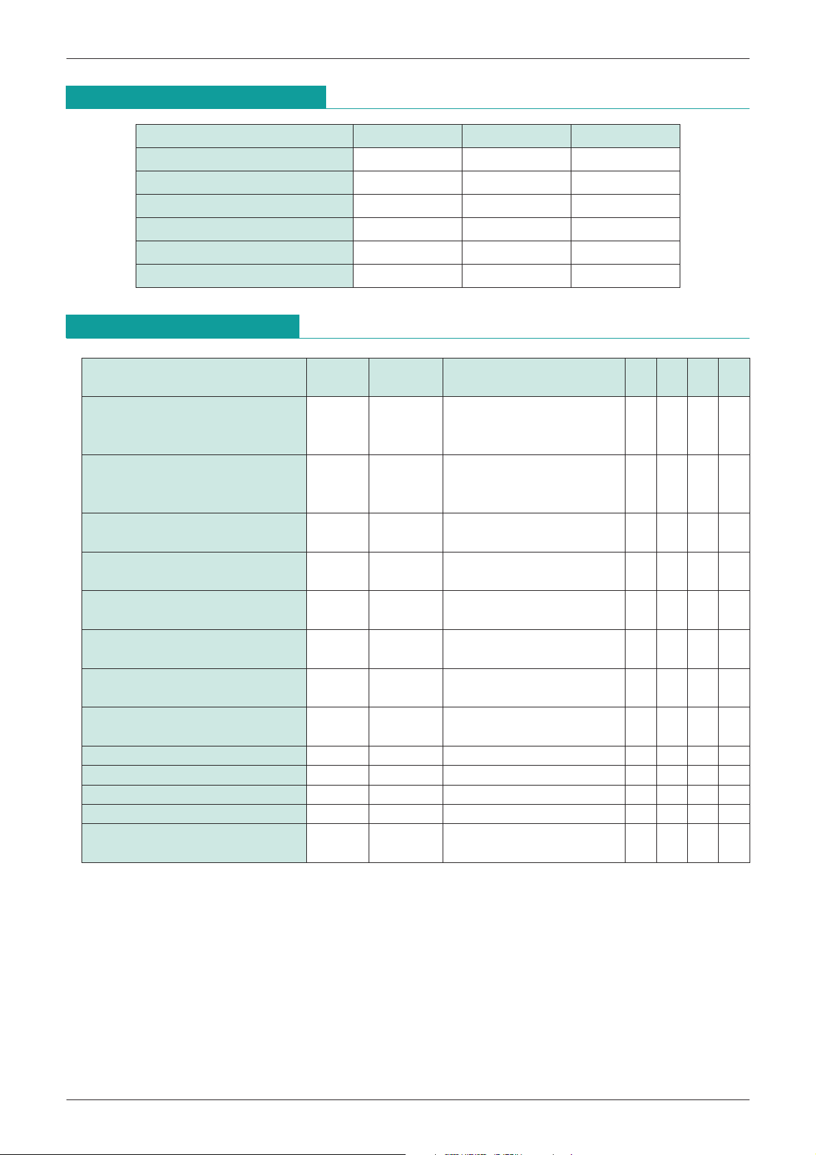
Absolute Maximum Ratings
Item Symbol Ratings Units
Storage temperature T
STG
Step-Up IC For EL Backlights MM1365
-
40~+125 °C
Operating temperature T
Power supply voltage V
Operating power supply voltage V
Voltage applied to O1, O2 output pins
Allowable loss Pd 300 mW
Electrical Characteristics
(Except where noted otherwise, Ta=25°C, VCC=1.5V, VCONT=1.5V)
Item Symbol
Consumption current for complete circuit 1
(under recommended circuit
operating conditions for EL)
Consumption current for 2 IC only
(under recommended circuit
operating conditions for EL)
Current consumption 3
(entire circuit off)
O1 pin output current
(charge signal)
O1 pin sync current
(charge signal) VCT2=0V
O2 pin output current
(discharge signal)
CT1 charge current
(Discharge setting pin) C
C
T2 charge current
(charge setting pin) C
C
T1 pin "H" threshold VTHH1 1 SW1 OFF, SW2 ON 0.65 V
C
T2 pin "H" threshold VTHH2 1 SW1 OFF, SW2 ON 0.65 V
C
T1 pin "L" threshold VTHL1 1 SW1 OFF, SW2 ON 0.15 V
C
T2 pin "L" threshold VTHL2 1 SW1 OFF, SW2 ON 0.18 V
Charge signal oscillation frequency
(C
T2 measurement) SW1 OFF, SW2 ON
OPR
CC max.
CCOP 0.95~+6 V
VO max.
Measurement
circuit
ICC11
ICC21
I
CC31VCONT
ISOU12
SIN 2
I
I
SOU2 2 VCT1=0V, VCT2=0V 1.00 1.80 3.00 mA
CT12
I
CT22
I
O1 output current measurement
fct2 1
-
20~+75 °C
-
0.3~+6 V
-
0.3~VCC V
Measurement conditions
C1=39nF, C2=1.5nF
SW1 OFF, SW2 ON
C1=39nF, C2=1.5nF
SW1 ON, SW2 OFF
=0V, SW1 ON, SW2 OFF
VO1=0V, VCT1=0.8V
VCT1=0V, VO1=0.3V
VCT1=0.3V, CT2=OPEN
T1 output current
VCT1=0V, VCT2=0.3V
T2 output current
C1=39nF, C2=1.5nF
Min. Typ. Max. Units
15 25 35 mA
1.3 2.5 4.5 mA
1.0 µA
25 50 75 µA
1.00 2.50 mA
1.2 2.0 2.7 µA
10 18 25 µA
20 kHz
 Loading...