

MITSMI MM1369AD, MM1354AJ, MM1354BD, MM1326AD Datasheet

MITSUMI
Q Xpander Processors MM1326, 1354, 1369
Q Xpander Processors
Monolithic IC MM1326, 1354, 1369
Outline
These ICs are analog stereo enhancement processors. They use patented Q Xpander technology to create a
stereo image with depth in three dimensions from ordinary left and right input channels.
There is no need for any special playback equipment; the enhanced audio effect can be experienced using
standard stereo audio equipment.
This IC, produced by Mitsumi, faithfully incorporates algorithms developed by Q Sound Labs, Inc., the world
leader in sound enhancement.
Features
1. Sound spreading sensation can be varied at will using an external VR (MM1354, MM1369)
2. Pseudo-stereo effects can be obtained from monaural audio signals (MM1369)
3. Sound spreading sensation can also be varied with a VR for pseudo-stereo from monaural input (MM1369)
4. Q Xpander on/off and pseudo-stereo on/off switching at TTL level
5. Internal filter circuit for few external components (MM1369)
6. No need for input signal encoding or special external equipment; playback possible using ordinary stereo
equipment
7. Low-noise design: 55 µVrms with Q Xpander on (MM1326)
60 µVrms with Q Xpander on (MM1354)
Package
SSOP-20A (MM1326AJ)
SDIP-22A (MM1326AD, MM1354AD, MM1354BD)
SSOP-24A (MM1354AJ)
SDIP-24A (MM1369AD, MM1369BD)
Applications
1. Computer sound boards
2. Active speaker systems
3. TV game equipment and other amusement devices
4. TVs, monitors, audio equipment
Line-Up
MM1326 MM1354 MM1369
Variable sound
spreading feature
Pseudo-stereo
function (spreading variable)
Operating power
supply voltage
Fixed Variable Variable
No No
4.5~10.0 (V) 4.5~12.0 (V) 8.0~10.0 (V)
Yes
MITSUMI
[MM1326]
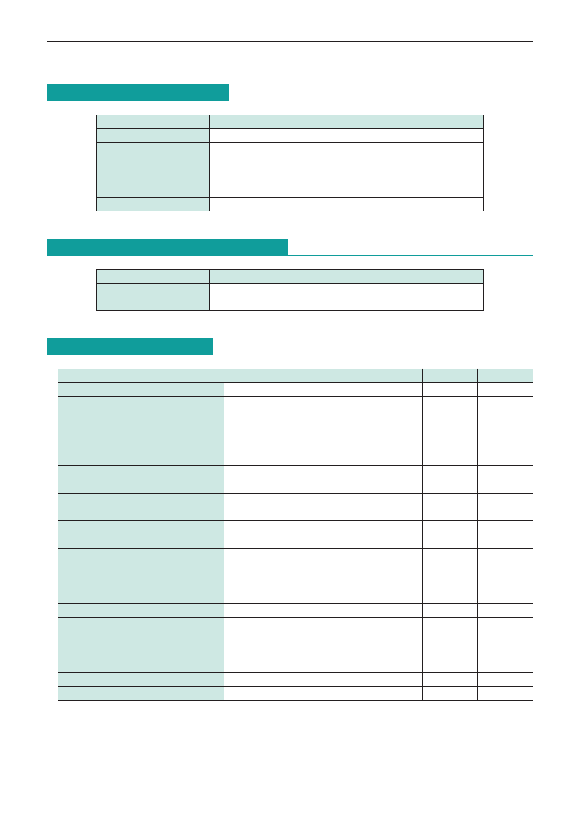
Absolute Maximum Ratings
Item Symbol Ratings Units
Storage temperature T
Operating temperature T
Power supply voltage V
Input voltage V
Output voltage I
Allowable loss Pd 500 mA
STG
OPR
CC max. 12 V
IN max. GND
O max. 10 mA
Recommended Operating Conditions
Item Symbol Ratings Units
Operating temperature T
Operating voltage V
OPR
OP 4.5~10.0 V
Q Xpander Processors MM1326, 1354, 1369
-
40~+125
-
20~+75
<
IN
V
=
-
20~+75
<
CC V
V
=
°
C
°
C
°
C
Electrical Characteristics
Item Measurement conditions Min. Typ. Max. Units
Consumption current 15 20 mA
Output voltage
Voltage gain Q Xpander 1 SG1: 1Vrms, 1kHz, SG2: no signal 5 6 7 dB
Voltage gain Q Xpander 2 SG1: 1Vrms, 1kHz, SG2: no signal
Voltage gain Q Xpander 3 SG1: no signal, SG2: 1Vrms, 1kHz 5 6 7 dB
Voltage gain Q Xpander 4 SG1: no signal, SG2: 1Vrms, 1kHz
Voltage gain bypass 1 SG1: 1Vrms, 1kHz, SG2: no signal
Voltage gain bypass 2 SG1: no signal, SG2: 1Vrms, 1kHz
Input resistance 21 30 39 kΩ
Power supply voltage rejection ratio V
Total harmonic distortion ratio Q Xpander
Total harmonic distortion ratio bypass
Output noise voltage Q Xpander
Output noise voltage bypass
SN ratio Q Xpander
SN ratio bypass
L-R channel balance L, R channels=1Vrms, 1kHz, Bypass=0V
Bypass pin voltage (H)
Bypass pin voltage (L)
Bypass pin voltage (H)
Bypass pin voltage (L)
1: Output voltage amplitude at f=1 kHz such that total output harmonic distortion is 1%
*
2: Voltage at which bypass pin (pin 2) is regarded as H (Q Sound mode)
*
3: Voltage at which bypass pin (pin 2) is regarded as L (bypass mode)
*
4: When Vbyp=5 V, current flowing into bypass pin (pin 2)
*
5: When Vbyp=0 V, current flowing from bypass pin (pin 2)
*
L, R channels=no signal, BW=20Hz to 20kHz, A curve
L, R channels=no signal, BW=20Hz to 20kHz, A curve
L, R channels=1Vrms, 1kHz, BW=20Hz to 20kHz, A curve
L, R channels=1Vrms, 1 kHz, BW=20Hz to 20 kHz, A curve
CC=9V+200mVrms, f=1kHz 44 50 dB
Lch=1Vrms, Rch=no signal
Lch=no signal, Rch=1Vrms
Lch=1Vrms, Rch=no signal
Lch=no signal, Rch=1Vrms
1 2 2.8 Vrms
*
2 2.1 V
*
3 0.7 V
*
4 350 µA
*
5
*
-
1 0.5 2 dB
-
1 0.5 2 dB
-
0.5 0 0.5 dB
-
0.5 0 0.5 dB
0.3 0.7 %
0.03 0.3 %
55 100
15 32
80 85 dB
90 95 dB
-
10 1dB
-
10 µA
µVrms
µVrms

MITSUMI
[MM1354]
Absolute Maximum Ratings
Item Ratings Units
Storage temperature
Operating temperature
Power supply voltage 15 V
Input voltage GND
Output voltage 10 mA
Allowable loss 650 mA
Recommended Operating Conditions
Item Ratings Units
Operating temperature
Operating voltage 4.5~12.0 V
Q Xpander Processors MM1326, 1354, 1369
-
40~+125
-
20~+75
<
V
=
-
20~+75
<
IN
CC V
V
=
°
C
°
C
°
C
Electrical Characteristics
Item Measurement conditions Min. Typ. Max. Units
Consumption current 16 21 mA
Voltage gain Q Xpander 1 SG1:1Vrms, 1kHz, SG2: no signal 3 4 5 dB
Voltage gain Q Xpander 2 SG1:1Vrms, 1kHz, SG2: no signal
Voltage gain Q Xpander 3 SG1: no signal, SG2: 1Vrms, 1kHz 3 4 5 dB
Voltage gain Q Xpander 4 SG1: no signal, SG2: 1Vrms, 1kHz
Voltage gain bypass 1 SG1:1Vrms, 1kHz, SG2: no signal
Voltage gain bypass 2 SG1: no signal, SG2: 1Vrms, 1kHz
Input resistance 21 30 39 kΩ
Input voltage amplitude (1)
Input voltage amplitude(2)
Total harmonic distortion ratio Q Xpander
Total harmonic distortion ratio bypass
Output noise voltage Q Xpander
Output noise voltage bypass
L-R channel balance L, R channels=1Vrms, 1kHz, Bypass=0V
Bypass pin voltage (H)
Bypass pin voltage (L)
Bypass pin voltage (H)
Bypass pin voltage (L)
1: Input voltage amplitude at f=1 kHz such that total output harmonic distortion is 1%. However, signals
*
input to SG1 and SG2 are in phase (phase difference 0
2: Input voltage amplitude at f=1 kHz such that total output harmonic distortion is 1%. However, signals
*
input to SG1 and SG2 are opposite in phase (phase difference 180
3: Voltage at which bypass pin (pin 22) is regarded as H
*
4: Voltage at which bypass pin (pin 22) is regarded as L
*
5: When Vbyp=5V, current flowing into bypass pin
*
6: When Vbyp=0V, current flowing from bypass pin
*
Lch=1Vrms, Rch=no signal, Lch=no signal, Rch=1Vrms
Lch=1Vrms, Rch=no signal, Lch=no signal, Rch=1Vrms
L, R channels=no signal, BW=20Hz to 20kHz, A curve
L, R channels=no signal, BW=20Hz to 20kHz, A curve
1 1 1.4 Vrms
*
2 0.5 0.7 Vrms
*
3 2.1 V
*
4 0.7 V
*
5 350 µA
*
6
*
°
).
°
).
-
1 0.5 2 dB
-
1 0.5 2 dB
-
5.6-5.1-4.6 dB
-
5.6-5.1-4.6 dB
0.4 1.0 %
0.03 0.3 %
60 100
15 32
-
10 1dB
-
10 µA
µVrms
µVrms
 Loading...