

MITSMI MM1248XF Datasheet
MITSUMI
Control of Lithium Ion Battery Charging and Discharging MM1248
Control of Lithium Ion Battery Charging and Discharging
Monolithic IC MM1248
Outline
This IC was developed for use in controlling charging and discharging of lithium ion batteries (battery modules
with three cells connected in series). In charging control, the voltage of the battery module as a whole is
controlled in constant-voltage control. Discharge control and monitoring of overvoltage rely on monitoring of
the voltages of individual cells.
Features
1. Charging control voltage VBATH=12.465V±1.5% (Ta=-20°C~70°C)
2. Overcharge detection voltage V
CELL=4.335V±1.5% (Ta=
-
20°C~70°C)
3. Internal circuit for setting dead time (for overvoltage detection, discharge control)
4. Low consumption current on overdischarge I
BATH3=1µA typ.
5. High-precision internal overvoltage detection startup circuit (cell voltage 4.2V or higher at end of charging)
Package
SOP-16B (MM1248XF)
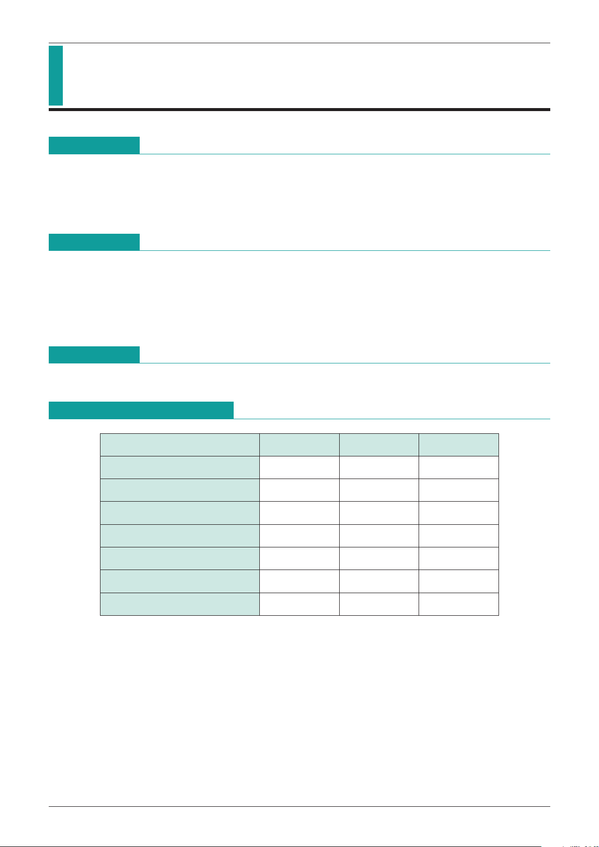
Absolute Maximun Ratings
(Except where noted otherwise, Ta=25°C)
Item Symbol Ratings Units
Storage temperature T
STG
-
40~+125 °C
Operating temperature T
OPR
-
20~+70 °C
Input voltage V
IN max. 18 V
Charge voltage V
BAT max. 15 V
Power supply voltage V
CC max. 15 V
Voltage applied to OV2 pin V
O2 max. 10 V
Allowable loss Pd 350 mW
MITSUMI
Control of Lithium Ion Battery Charging and Discharging MM1248
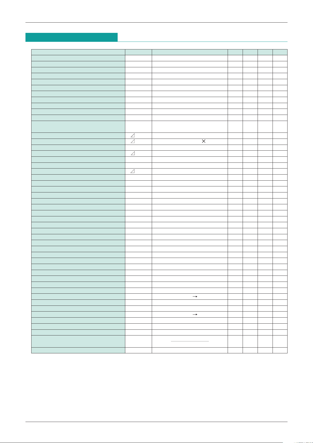
Electrical Characteristics
(Except where noted otherwise, Ta=25°C, VIN=15 V, CON=VIN)
Item Symbol Measurement conditions Min. Typ. Max. Units
Consumption current 1(pin V
IN) VIN VIN=15V, CON=0V 250 350 µA
Consumption current (pin V
CC) 1 ICC1VCELL=4.4V 2.1 2.6 mA
Consumption current (pin V
CC) 2 ICC2VCELL=4.2V, CON=0V 1.5 2.0 mA
Consumption current (pin V
CC) 3 ICC3VCELL=4.2V, CON=VIN 1.0 1.3 mA
Consumption current (pin V
CC) 4 ICC4VCELL=4.0V 50 100 µA
Consumption current (pin V
CC) 5 ICC5VCELL=2.4V 0.1 µA
Consumption current (pin B
ATH) 1 IBATH1VCELL=4.4V 5.0 10.0 µA
Consumption current (pin B
ATH) 2 IBATH2VCELL=4.0V 2.5 5.0 µA
Consumption current (pin B
ATH) 3 IBATH3VCELL=2.4V 1.0 2.0 µA
Charging control voltage V
BATH Ta=
-
20~70°C
12.270 12.465 12.670
V
Overcharge detection voltage V
CELLU Ta=
-
20~70°C
4.270 4.335 4.400
V
Overcharge reset voltage V
CELLO
V
CELL
UV
CELL
UV
CELL
U
-
60mV-45mV-30mV
V
Sensing voltage margin 1 V
UO1VBATH/3
-
VCELLU 100 mV
Sensing voltage margin 2 V
UO2VBATH
-
VCELLU 3 300 mV
Overvoltage sensing operation voltage V
ALM 4.05 4.20 4.35 V
Overvoltage sensing hysteresis voltage
VALM 50 90 130 mV
Overdischarge detection voltage V
CELLS 2.31 2.40 2.49 V
Discharge resume voltage V
CELLD 2.49 2.65 2.81 V
Overdischarge sensing hysteresis voltage
VCSDVCELLD-VCELLS 175 250 325 mV
Pin 11 input current 1 I11 V
CELL=4.0V 100 200 300 nA
Pin 11 input current 2 I11A V
CELL=4.4V 0.7 1.0 1.3 µA
Pin 13 input current 1 I13 V
CELL=4.0V 100 200 300 nA
Pin 13 input current 2 I13A V
CELL=4.4V 0.7 1.0 1.3 µA
Pin 14 input current I14 V
CELL=4.0V 7.7 10.0 14.3 µA
CON pin threshold voltage V
THCON
VIN-
1.8 VIN-
0.4
V
CON pin input current I
INCON VIN
-
CON=1.8V 100 µA
CON pin leakage current I
LCON VIN
-
CON=0.4V 1.0 µA
CHG pin pull-up resistance R
CHG
Resistance across pins VINand C
HG
14 20 26 kΩ
CHG pin sync current IS
CGH VBATT<12V 100 µA
CHG pin output voltage L V
THCHLVIN
-
CHG, ICGH=20µA 6.2 V
CHG pin output voltage H V
THCHHVIN
-
CHG, ICGH=20µA 0.4 V
DCHG pin source current I
SODCH 20 µA
DCHG pin sync current I
SIDCH 20 µA
DCHG pin output voltage L V
THDCLBATH
-
DCHG, IS=20µA 1.0 V
DCHG pin output voltage H V
THDCHDCHG
-
GND, IS=-20µA 0.8 V
OV2 pin sync current I
SOOV2 100 µA
OV1 pin source current I
SOOV1 100 µA
OV1 pin pulldown resistance RO
V1 355065kΩ
CCC pin charge current IC
CC VCELL=4.4V, CCC=3.0V 150 220 290 nA
CCC pin threshold voltage V
THCCC CCC=0V 5V 4.10 4.30 4.50 V
CCC initialization delay time TI
NT CCC=0.068µF 10 mS
CDC pin charge current IC
DC VCELL=2.8V, CCC=3.0V 260 380 500 nA
CDC pin threshold voltage V
THCDC CCC=0V 5V 4.20 4.40 4.60 VC
Overvoltage sensing dead time TDC
CC CCC=0.068µF 0.5 1.0 1.5 S
Overdischarge sensing dead time TDC
DC1CDC=0.1µF 0.5 1.0 1.5 S
Overdischarge reset dead time TDC
DC2CDC=0.1µF 0.5 1.0 1.5 S
Battery voltage monitor output
VB
MON
-
1.0 0 1.0 %
voltage ratio
Battery voltage monitor output current
ILMON 50 µA
(BATH-GND) ÷3
V
BATT

MITSUMI
Control of Lithium Ion Battery Charging and Discharging MM1248
Timing Chart
V
IN
C
ON
B
ATH
B
ATL
C
DC
D
CHG
V
BAT
O
V2
C
CC
O
V1
B
ATM
tDC
DC1
tDC
CC
tDC
DC2
Unsettled Unsettled
Block Diagram
 Loading...