

MITSMI MM1104CF, MM1104BF Datasheet
MITSUMI
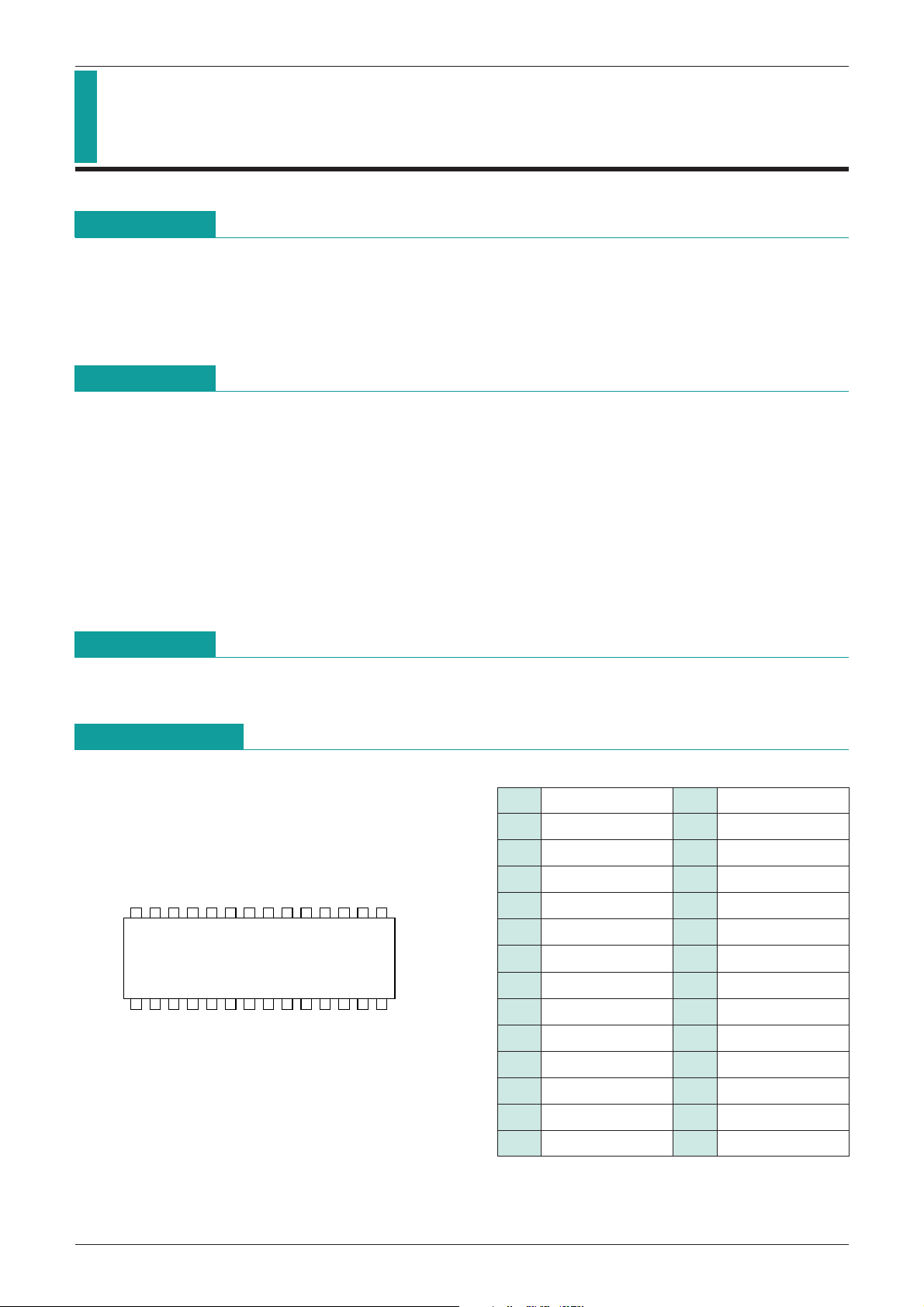
SOP-28B
13 6
10
24587129
11 1413
28 24 2127 25 23 22 2026 1517 161819
IC for Headphone Stereos MM1104
IC for Headphone Stereos
Monolithic IC MM1104
Outline
This IC was developed for use in 3 V headphone stereos. It incorporates all the basic functions of tape
players.
Mitsumi has previously offered the LAG665, LAG668, LAG673 and MM1006 as one-chip versions. However,
this IC is the result of a through review and redesign extending to circuit details.
Features
1. Configuration: Pre-and power amp, motor control
2. Adoption of shock noise prevention circuitry
Through the use of a circuit which suppresses noise occurring when the power supply is turned on and off,
noise output is reduced without muting.
3. Stable motor speed control circuit
A bridge circuit employing power transistors provides motor speed control with minimal drift.
4. Preamp off pin is convenient for radio connections
5. Radiation pin: When radio wave-induced noise is a problem, this pin can be used to cut the frequency
characteristic.
Package
SOP-28B (MM1104AF, MM1104BF, MM1104CF)
Pin Assignment
1 1/2VCC 15 N.C
2 Pre
3 NFB1 17 Phase
4 PreOUT1 18 V
5 Pre Off 19 PowerOUT2
6 Power
7 Radiation1 21 Filter
8 PowerOUT1 22 Radiation2
9 GND 23 Power
10 Governor V
11 N.C 25 PreOUT2
12 PCOUT 26 NFB2
IN1 16 Speed
S
IN1 20 Amp VCC
IN2
CC 24 N.C
13 GND 27 Pre
14 Governor GND 28 Amp GND
IN2
MITSUMI
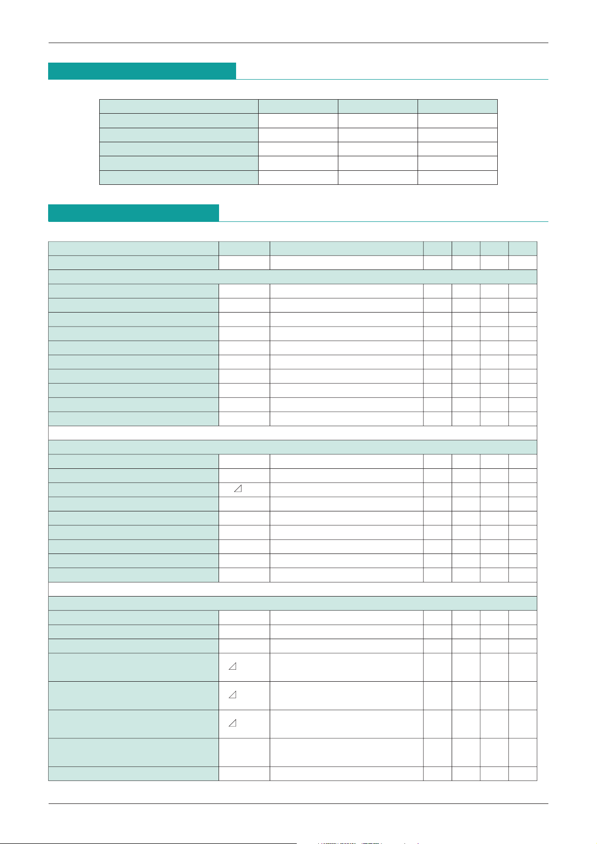
Absolute Maximum Ratings
Item Symbol Ratings Units
Operating temperature T
Storage temperature T
Power supply current V
Power consumption Pd 700 (Ta=25
Operating voltage Vop +2.0~+5.0 V
OPR
STG
CC
IC for Headphone Stereos MM1104
-
20~+65
-
40~+125
-
0.3~+7.5 V
°
C) mW
°
C
°
C
Electrical Characteristics
(Except where noted otherwise, Ta=25°C)
Item Symbol Measurement conditions Min. Typ. Max. Units
Consumption current I
Preamp unit (Ta=25
Open-circuit gain GVo Vo=
Closed-circuit gain GVc Vo=
°
C)
CC Amp. only 11 18 mA
-
10dBm f=100Hz 86 dB
-
10dBm 42 dB
Maximum output voltage Vom THD=10% 0.5 0.74 Vrms
Total harmonic distortion ratio THD Vo=
Output noise voltage Vno Rg=2.2kΩ, CCIR waiting 240 500
-
10dBm 0.06 0.5 %
µVrms
Crosstalk between channels CHCT Vo=-10dBm 45 60 dB
Ripple rejection RR V
Output voltage with preamp off VoOff Vo=
CC=3V, VR=
-
10dBm, when pre operation
-
20dBm, fR=100Hz 30 42 dB
-
100-70 dBm
Input resistance with preamp off RiOff 7 10 13 kΩ
Output resistance with preamp off RoOff 7 10 13 kΩ
Measurement conditions: Except where noted otherwise, V
Power amp unit (Ta=25
°
C)
CC=3V, Rg=2.2kΩ, RL=30kΩ, f=1kHz
Input resistance Ri 14 20 26 kΩ
Voltage gain Gv Po=5mW 32 34 36 dB
Voltage gain difference between channels
Maximum output power I Pom1 THD=10%, R
Maximum output power II Pom2 THD=10%, R
Gv 0 2 dB
L=16Ω 40 62 mW
L=32Ω 20 34 mW
Total harmonic distortion ratio THD Po=5mW 0.4 2 %
Crosstalk between channels CH
Output noise voltage Vn Rg=1kΩ, CCIR waiting 150 300
CT Po=5mW 45 62 dB
µVrms
Ripple rejection RR VCC=3V, VR=-20dBm, fR=100Hz 40 50 dB
Measurement conditions: Except where noted otherwise, V
°
Motor governor (Ta=25
C)
Consumption current Id A
Startup current I
MS IM measured when RV=1.5Ω 500 mA
CC=3V, Rg=1kΩ, RL=16Ω, f=1kHz
2 measured 2.0 7.0 mA
Reference voltage Vref V5 measured with SW12 off 0.09 0.10 0.11 V
Reference voltage fluctuation I Vref1
Reference voltage fluctuation II Vref2
Reference voltage fluctuation III Vref3
Output saturation voltage VoSAT
I
Reference voltage V8 measured
VS fluctuation for
V
CC=1.5 to 3.5V, VCC=3.0V ref.
VS fluctuation for
M=25 to 200m A, IM=100mA ref.
VS fluctuation for
Ta=
-
10 to 60°C, Ta=25°C ref.
M=200mA with SW12 on
I
0.1 0.5 %/V
0.005 0.05
%/mA
0.01 %/
0.2 0.3 V
Bridge ratio K V7/V6 measured 9 10 11
°
C
 Loading...