

MITSMI MM1035XF, MM1035XD Datasheet
MITSUMI
System Reset (with built-in watchdog timer) MM1035
System Reset (with built-in watchdog timer)
Monolithic IC MM1035
Outline
This IC functions in a variety of CPU systems and other logic systems to generate a reset signal and reset the
system accurately during momentary interruption or lowering of power supply voltage.
It also has a built-in watchdog timer for operation diagnosis. This prevents the system from running wild by
generating an intermittent reset pulse during system mis-operation.
Features
1. Built-in watchdog timer
2. Low minimum operating voltage V
3. Both positive and negative logic reset output can be extracted
4. Accurate detection of drop in power supply voltage
5. Detection voltage has hysteresis
6. Few external parts 1 capacitor
CC=0.8V typ.
Package
DIP-8A (MM1035XD)
SOP-8A (MM1035XF)
Applications
Microcomputers
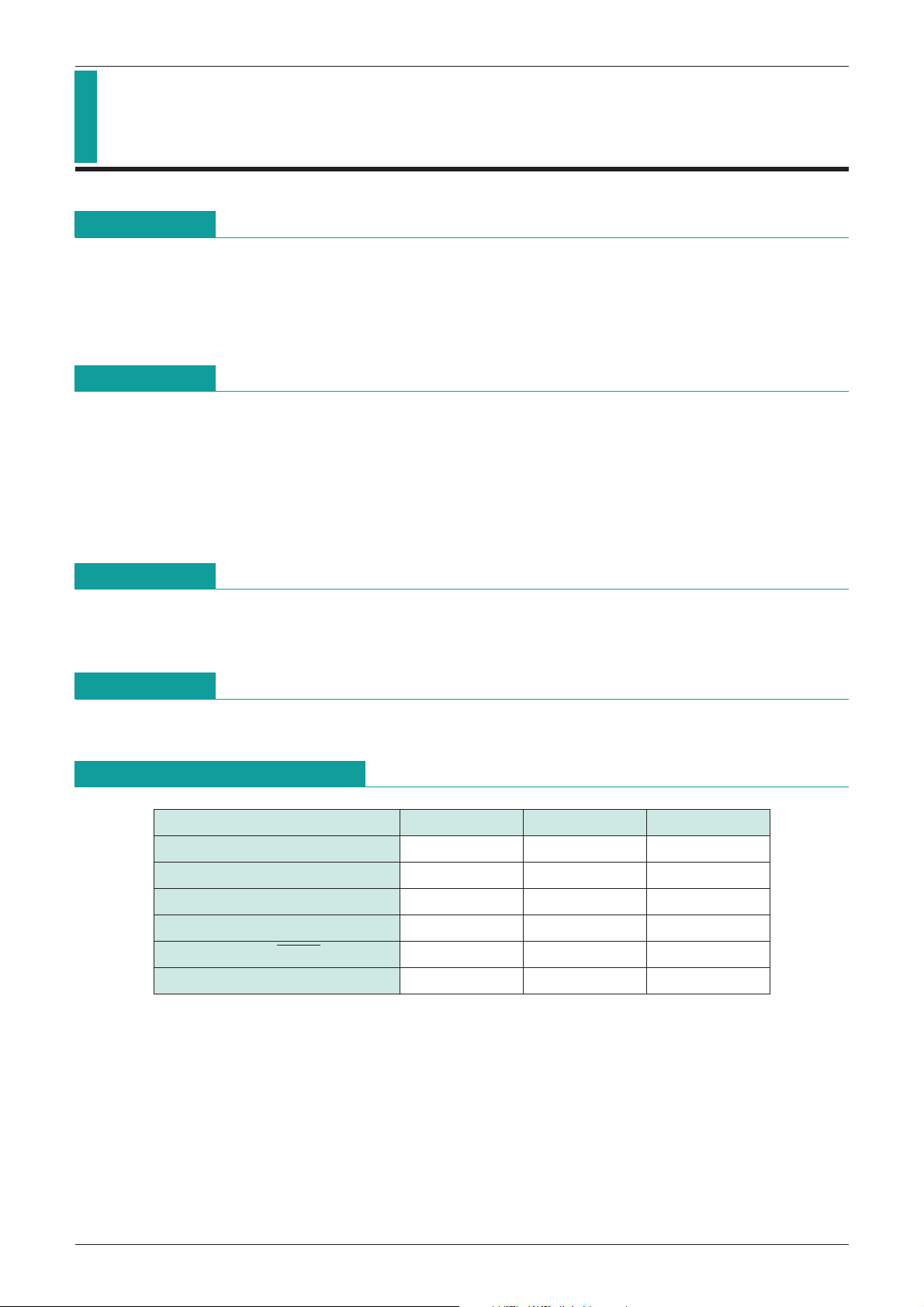
Absolute Maximum Ratings
Item Symbol Rating Units
Storage temperature T
Operating temperature T
Power supply voltage V
Voltage applied to VS & CK pins V
Voltage applied to RESET, RESET pin
Allowable loss Pd 400 mW
(Ta=25°C)
STG
OPR
CC max.
VS & VCK
VOH
-
40~+125
-
20~+70
-
0.3~+10 V
-
0.3~+10 V
-
0.3~+10 V
°
C
°
C
MITSUMI
System Reset (with built-in watchdog timer) MM1035
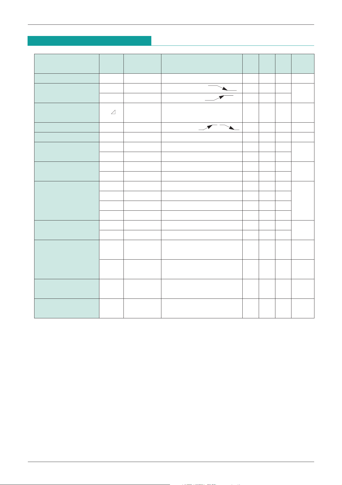
Electrical Characteristics 1 (DC)
Item Symbol
Consumption current I
Detection voltage
Detection voltage
temperature coefficient
Hysteresis voltage V
CK input threshold V
CK input current
Output voltage (High)
Output voltage (Low)
V
S/ T 1 ±0.01 %/°C
V
V
V
V
V
Measurement
circuit
CC 1
V
SL 1 4.05 4.20 4.35
SH 1 4.15 4.30 4.45
V
HYS 1 50 100 150 mV
TH 1 0.8 1.2 2 V
I
IH 1VCK=5V 0 1
IL 1VCK=0V
I
OH11 I=
OH21 IRESET=
OL1 1 I =3mA, VS=0V 0.2 0.4
OL2 1 I =10mA, VS=0V 0.3 0.5
OL31 IRESET=0.5mA, VS=OPEN 0.2 0.4
(Except where noted otherwise, Ta=25°C, VCC=5V, measurement circuit 1)
Measurement conditions Min. Typ. Max. Units
During watchdog timer operation
VS=OPEN, VCC
0.7 1.0 mA
V
VS=OPEN, VCC
VSH-VSL, VCC
µA
-
-----------------------------------------
RESET
20-10
-
5µA, VS=OPEN 4.5 4.8
-
3
V
-
5µA, VS=0V 4.5 4.8
-----------------------------------------
RESET
-----------------------------------------
RESET
V
V
OL41 IRESET=1mA, VS=OPEN 0.3 0.5
I
OL1 1 V =1.0V, VS=0V 10 16
Output sink current
I
OL21 VRESET=1.0V, VS=OPEN 1 2
CT11
I
C
T charge current
ICT21
Minimum operating power
supply voltage to ensure RESET
------------------------------------------------
VCCL1 1 0.8 1.0 V
Minimum operating power
supply voltage to ensure RESET
------------------------------------------------
VCCL21
-------------------------------------------
RESET
VTC= 1.0V during watchdog
timer operation
VTV= 1.0V during power
on reset operation
--------------------------------------------
RESET
V =0.4V
------------------------------------------------
RESET
I =0.2mA
I
RESET=VCC
R
L
2 (between Pin 2 and GND) =1MΩ
-
0.1V
-
8
-
12-24 µA
-
0.8-1.2-2.4 µA
0.8 1.0 V
mA
MITSUMI
System Reset (with built-in watchdog timer) MM1035
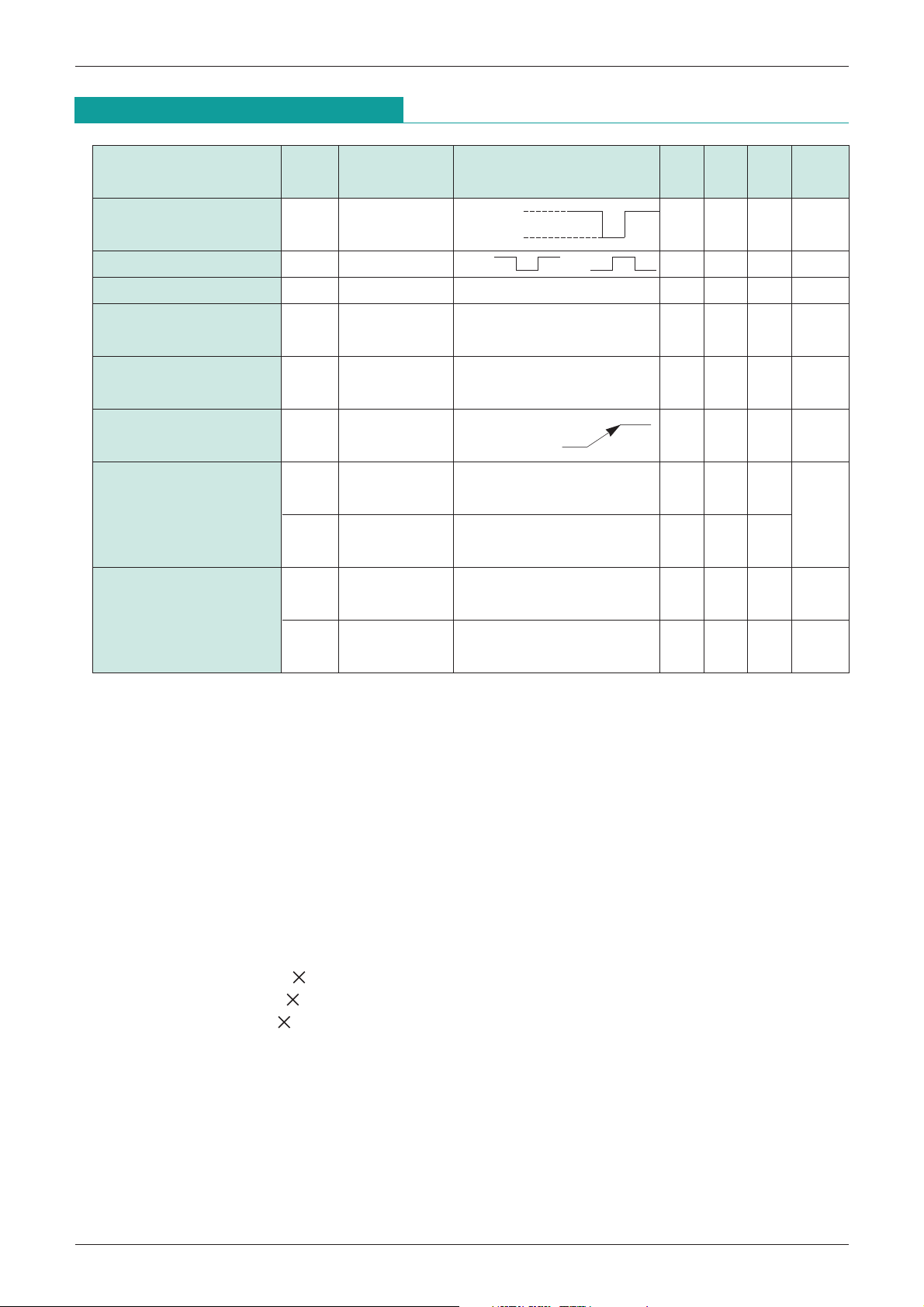
Electrical Characteristics 2 (AC)
(Except where noted otherwise, Ta=25°C, VCC=5V, measurement circuit 2)
Measurement
Item Symbol
Measurement conditions Min. Typ. Max. Units
circuit
5V
CC input pulse width TPI 28µS
V
VCC
4V
CK input pulse width T
CK input cycle T
CKW 23µS
CK 220µS
CK or
Watchdog timer
WD 2CT=0.1µF 5 10 15 mS
monitoring time
1
*
T
Reset time for
WR 2CT=0.1µF 1 2 3 mS
watchdog timer
2
*
T
Reset hold time for
power supply rise
Output delay time from V
3
*
CC
T
PD12
T
CT=0.1µF, VCC
---------------------------------------
RESET
pin
RL1=2.2kΩ, CL1=100pF
210
PR 2 50 100 150 mS
µS
4
*
Output rise time
5
*
PD22
T
R12
t
R22
t
RESET pin
L2=10kΩ, CL2=20pF
R
----------------------------------------
RESET
pin
RL1=2.2kΩ, CL1=100pF
RESET pin
L2=10kΩ, CL2=20pF
R
310
1.0 1.5
µS
1.0 1.5 µS
Notes :
1: Monitoring time is the time from the last pulse (negative edge) of the timer clear clock pulse, until reset
*
pulse output. In other words, reset output is output if a clock pulse is not input during this time.
2: Reset time means reset pulse width. However, this does not apply to power on reset.
*
3: Reset hold time is the time from when VCC exceeds detection voltage (VSH) during power on reset, until
*
---------------------------------------
RESET
4: Output delay time is the time from when power supply voltage drops below detection voltage (VSL), until
*
---------------------------------------
RESET
5: Voltage range when measuring output rise and fall is 10~90%.
*
6: Watchdog timer monitoring time (TWD), watchdog timer reset time (TWR) and reset hold time (TPR) during
*
power supply rise can be changed by varying C
formulae. The recommended range for C
output goes high (reset release).
output goes low (reset status).
PR (mS)
T
T
WD (mS)
T
WR (mS)
.
=. 1000 CT (µF) Example : When CT=0.1µF
.
=. 100 CT (µF) TPR.=. 100mS
.
=. 20 CT (µF) TWD
T capacitance. The times are expressed by the following
T is 0.001~10µF.
.
=. 10mS
.
T
WR
=. 2mS
 Loading...