

MITSMI LAG640D Datasheet
MITSUMI
IC for Multifunction Telephones LAG640
IC for Multifunction Telephones
Monolithic IC LAG640
This IC was developed for use in multifunctional telephones with security features; it has the following
functions.
Features
1. Incorporates efficient switching regulator with broad input voltage range
V
OUT 5V±0.25 IL 250mA (13~45V)
V
IN 15~45V
2. Internal data transmission/reception circuits
Data can be superposed on the power supply line for transmission.
Can be switched between two different input modes
3. Internal system reset circuit
5V line abnormal voltage detection circuit
Watchdog timer reset circuit
4. Internal speaker amp
260 mW typ. at 8Ω load
Mute pin
5. Internal beep sound generator circuit
With pin to vary audio volume (also used to turn beep sound on and off)
Package
SDIP-30A (LAG640D)
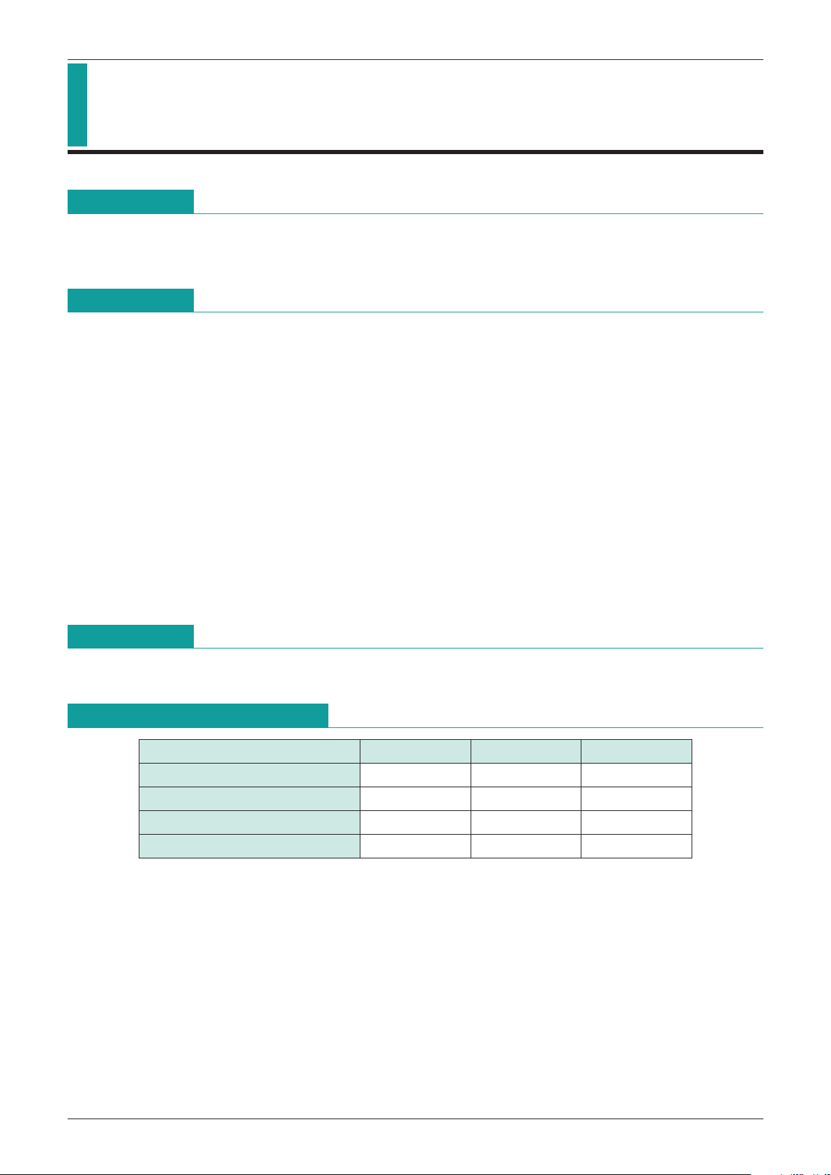
Absolute Maximum Ratings
(Ta=25°C)
Item Symbol Ratings Units
Operating temperature T
OPR
-
20~+70
°
C
Storage temperature T
STG
-
40~+125
°
C
Power supply current V
CC max. 46 V
Allowable loss Pd 750 mW
Outline
MITSUMI
IC for Multifunction Telephones LAG640
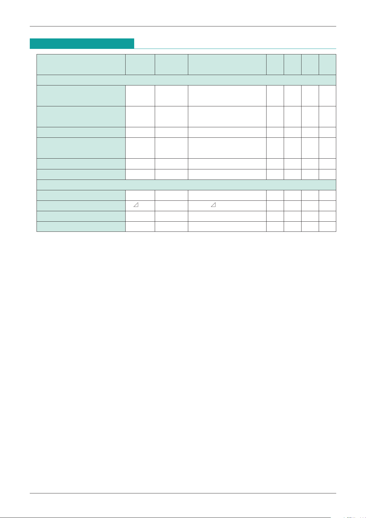
Electrical Characteristics
(Except where noted otherwise, Ta=25°C, VCC=30V)
Item Symbol
Measurement
Measurement conditions Min. Typ. Max. Units
circuit
SWR unit
Output voltage (5V) V
O11
V
CC=15~45V
4.75 5.00 5.25 V
I
L=0~250mA
Output voltage (5V) V
O21
V
CC=13~45V
4.70 5.00 5.25 V
I
L=0~200mA
Output ripple voltage Vr 1 I
L=250mA 50
mV
P-P
Reactive current ICCq1
I
L=0mA
610mA
Amp & Transmission unit
SWR oscillation frequency F
OSC 180kHz
Output current on short-circuit I
OS 1RS=0.2Ω 70 110 150 mA
Power supply voltage detection unit
Detection voltage V
S 2
*
4.30 4.50 4.80 V
Detection drop voltage V
S 2VS=Vo
-
VS 0.2 V
Output current while on IR
ON 2 Vo=4V 10 20
mA
Leakage output current while off
IROFF 2 Vo=5.25V 1 µA
Note: The asterisk (*) indicates that the power supply voltage detection unit characteristics are standards in
the transient power on/off states. However, for convenience the detection voltage is taken to be the
value of V
0 when V0 in measurement circuit 2 is varied and the pin 6 output state is switched from off
to on.
MITSUMI
IC for Multifunction Telephones LAG640
Electrical Characteristics
(Except where noted otherwise, Ta=25°C, VCC=30V Faudio=1kHz)
Item Symbol
Measurement
Measurement conditions
Min. Typ. Max. Units
circuit
Power amp unit
Amp gain G
V 1 Voa=0.775Vrms 37 40 43 dB
Maximum distortion-free output
PO max. 1 THD=10% 150 260 mV
Distortion THD 1 P
O=100mW 5 %
Attenuation at 100 Hz GF1/GF0 1
F
O=1kHz, Fl=100Hz
-
14 dB
Voa=0.775Vrms
Attenuation at 10 Hz GF2/GF0 1 F2=10 kHz, above conditions
-
8dB
Input IMP 1 R
IN1 3 Mute off 10 15 kΩ
Input IMP 2 R
IN2 3 Mute on 2.5 3.5 kΩ
Mute on
Residual noise 1 Vno1 1
AUDIO IN 20mVrms
0.5
mVrms
IL=10 70mA 1.5kHz
Transmission unit on Ft=1kHz
Mute off
Residual noise 2 Vno2 1
AUDIO OFF
1.2
mVrms
IL=10 70mA 1.5kHz
Transmission unit on Ft=1kHz
Beep sound generator unit
Beep sound frequency Fb 1 0.85 1.0 1.15 kHz
Beep off switching point Ibsw 1 Pin 9 input current 20 35 48 µA
Beep sound output 1 Vob1 1
Pin 9 connected to GND through 4.7k
1.0 1.4 1.8 Vrms
Amp output voltage
Beep sound output 2 Vob2 1
Pin 9 connected to GND through 47k
0.11 0.16 0.22 Vrms
Watchdog timer unit
Timer time Tt 1
cf. watchdog timer
2.4 3.0 3.6 S
waveform diagram
cf. watchdog timer
0.45 1.1
Output pulse width T
PW 1 waveform diagram mS
T=beep sound period
(1/2T)
(1T)
Output voltage while on Vw
ON 1 0.5 V
Leakage output current while off
IwOFF 11µA
Timer-clearing pulse width Tcl 1 5 µS
Transmission circuit unit
Transmission output voltage (1)
Vto1 2
R
L-110Ω, peak value
5.1 5.8 6.6
Vp-p
across pins L3-L4
Transmission output voltage (2)
Vto2 2
R
L-1Ω, peak value
5.5 6.2 7.0
Vp-p
across pins L3-L4
L3 pin voltage VL3 2 No signal 4.0 4.4 4.8 V
L4 pin voltage VL4 2 No signal 0.5 0.7 0.9 V
Reception sensitivity Vrs 2 0.8 1.0 1.2
Vp-p
Input IMP RIN3 4 Both pins 7and 8 14 20 26 kΩ
Transmission delay time Td1 2
cf. transmit/receive
0.4 µS
waveform diagrams
Transmission delay time Td2 2
cf. transmit/receive
0.4 µS
waveform diagrams
Transmission delay time Td3 2
cf. transmit/receive
0.8 µS
waveform diagrams
Transmission delay time Td4 2
cf. transmit/receive
0.8 µS
waveform diagrams
Reception output H voltage VroH 2 R
L=10kΩ 4.5 V
Reception output L voltage VroL 2 R
L=1.5kΩ 0.5 V
General logic unit characteristics
H level input voltage ViH 3 2.4 V
L level input voltage ViL 3 0.8 V
H level input current IiH 3 V
IN=2.4V 10 µA
L level input current IiL 3 V
IN=0.4V
-
300 µA
 Loading...