

Page 1

2450 A!amo SE
Albuquerque. NM 87t06
Page 2

PRELIMINARY DOCUMENTATION RELEASE
THE FOLLOWING INFORMATION IS A PRELIMINARY RELEASE ONLY.
THE COMPLETE THEORY OF OPERATION WILL BE ADDED TO THE
ASSEMBLY MANUAL AT A LATER DATE. THE OPERATORS MANUAL
AND DOS DOCUMENTATION WILL BE DEVELOPED IN A SINGLE
MANUAL ALSO. BOTH OF THESE, AND ANY UPDATES TO THIS
ENTIRE SYSTEM DOCUMENTATION WILL BE SENT IMMEDIATELY
UPON THEIR PRINTING DATE.
Page 3

OISK OPERATORS MANUAL
INSCRIPTION OF SYSTEM
A) DISK SPEC SHEET
B) OISK SYSTEM BLOCK DIAGRAM DESCRIPTION
1. CONTROLLER BOARD 1:
Controller Board 1 does all input functions to the ALTAIR
bus (Read Data, Sector Data, Status Information), as well
as Control Addressing of all Disk to ALTAIR I/O.
2. CONTROLLER BOARD 2:
Controller Board 2 performs all output functions from the
ALTAIR bus (Write Data, Disk Control, Disk Enable and
Drive Selection).
3. INTERCONNECT CABLE:
An 18 pair flat cable with two 37 pin connectors, a male
on one end, a female on the other. This cable connects the
Disk Drive to the ALTAIR Disk Controller and "Daisy Chains"
one Disk Drive to another in multiple Disk systems.
4. OISK DRIVE CABINET:
a) POWER SUPPLY:
The Disk Drive Cabinet contains a power supply for powering
the Disk Buffer and Disk Drive.
b) THE DISK BUFFER:
The Disk Buffer board contains the necessary line drivers
and receivers for interconnection with long cables to the
Disk Drive. In addition, it contains the Disk Drive Address
circuitry that allows the Controller to select one of 16
Disk Drives.
The Disk Buffer board also contains the line drivers for
connection of multiple Disk Systems.
c) THE DISK DRIVE:
The Disk Drive, a Pertec F0-400, contains the mechanism and
electronics that actually reads ar.d writes data on the Diskette.
Page 4
CONNECTION OF OISK SYSTEM:
A) CONTROLLER BOARDS:
1. Items Supplied:
a) CONTROLLER BOARD 1 (white vert strips)
b) CONTROLLER BOARD 2 (with short cable wired to it)
c) CONTROLLER CABLE (with 37 pin on one end, 3 Molex connec-
tors on the other end)
d) Connector Mounting Bracket and Hardware
2. Connection of Controller Boards
a) Take cover off ALTAIR (power off!)
b) Feed Molex (flat) connector ends of Controller cable through
hole in back of ALTAIR on connector panel: (37 pin con-
nector outside chassis, molex connectors inside chassis).
c) Lay board 1 flat in front of you on the ALTAIR chassis with
components up and stab connector to your right (as facing
the front of the ALTAIR).
d) Take the short wired cable of board 2 and connect it to the
20 pin connector on board 1 (note polarization key of
connector and missing pin on the PC board).
e) Place board 2 flat, to the left of board 1.
f) Connect 20 pin Molex connector on the Controller cable to
the 20 pin connector on board 2. Note Keying.
g) Take the 10 pin connector on the Controller cable with the
orange and yellow wires connected to it and connect it
to the 10 pin connector on board 2. Note Keying.
h) Take the remaining 10 pin connector on the Controller cable
with white and gray wires on it and connect it to the
10 pin connector on board 1. Note Keying.
i) Take both boards, hold together and slide into slots, with
board 1 on right, board 2 on the left. Be sure wires
from connector go out between card guides, and do not
catch on card guides,
j) Push cards firmly into connector in ALTAIR mother board,
k) Install 37 pin connector in bracket and on back of ALTAIR,
straddling 2 connector holes. Use #4-40 x 5/16 screws,
lockwashers and #4-40 nuts.
B) DISK DRIVE CONNECTION TO ALTAIR:
Take the 6 ft. flat cable with 1 male and 1 female connector;
connect male end to Disk Controller connector on ALTAIR, and
female end to connector on the Oisk Drive marked "To Controller".
Page 5

THE ALTAIR FLOPPY
D!SK SYSTEM
The ALTA/R Disk offers the advantage of nonvolatile memory
plus relatively fast access to datu The AL7A/R Disfc Controffer
consists of tv,o PC boards lover 60 IC s) that fit in [he AL7A1R
nect to the disk through a 37 pin connector mounted on the
back of the ALTAIR Data is transferred to and from the disk
senally at 250K bits sec The disk controller converts the senal
data to and from Sbit parallel words (one word every 32 « sec!
The ALTA/R CPU transfers the data, word by word to and from
memoty. depending on wnether the disk is reading or writing
The disk controller also controls all mechanical functions of the
disk as well as presenting disk status to the computer All timing
tasks Since the /loppy diskette is divided into 32 sectors, a
hardware interrupt system can be enabled to notify the CPU at
The Disk Dnve unit, using a PERTEC FD400 mounted in an
Optima case 15'?" high—same depth and width as computer),
includes a poaer suppfy PC board and a 8u//er Address Line
temperature ior continuous operation The disk dnve cabinet
has two 37 pin connectors on the back panel, one is the input
from the disk controller, the other is the output to additional disk
dnves Up to ]6 dnves may be attached to one controller
The Mb DCDD consists of the disk controller and one disk
dnve with an interconnect cable The
MM
Disk is one disk dnve for
adding storage capability to the
MM
DCDD and includes the inter
The AL7AJR Disk Format allows storage of over 300.000
bytes. Since the disk is hard sectored 132 sectors for each track),
we wnte 137 byies on each sector. 9 of which are used internally
[tracks checksum) leaving 128 data bytes per sector. 4096 per
track One floppy diskette is supplied with each drive: extra flop-
pies are available for purchase A so/Mare driver for the floppy
disk is available at no charge and is supplied with the disk as a
source listing The disk operating system—which has a complete
file structure and utilities for copying, deleting and sorting
files—costs extra Extended BASIC. which uses random and se-
quential tile access for the floppy disk, is also available.
Speed
Access Times
Head Life
Disk Life
Rate
Power
Diskette
Specifications
360 rpm 1166.7 ms/rev)
Track to track. 10 ms
Head settle. 20 tin
Average time to read or
write. 400 nis
Worst case. 1 sac
Over 10.000 hours of head
to disk contact
Over 1 million passes/track
250K bits/sec
117VACH0W
Dysan 101 floppy disk. 77 tacit*
Page 6
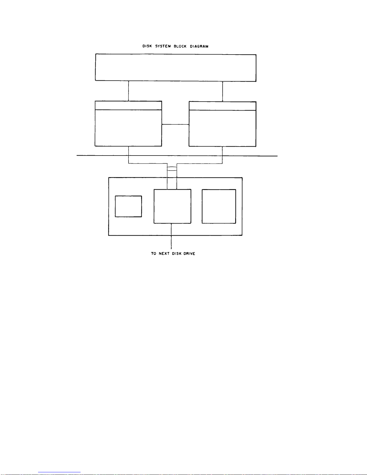
DISK SYSTEM BLOCK DIAGRAM
10 NEXT DISK DRIVE
Page 7
r
Page 8
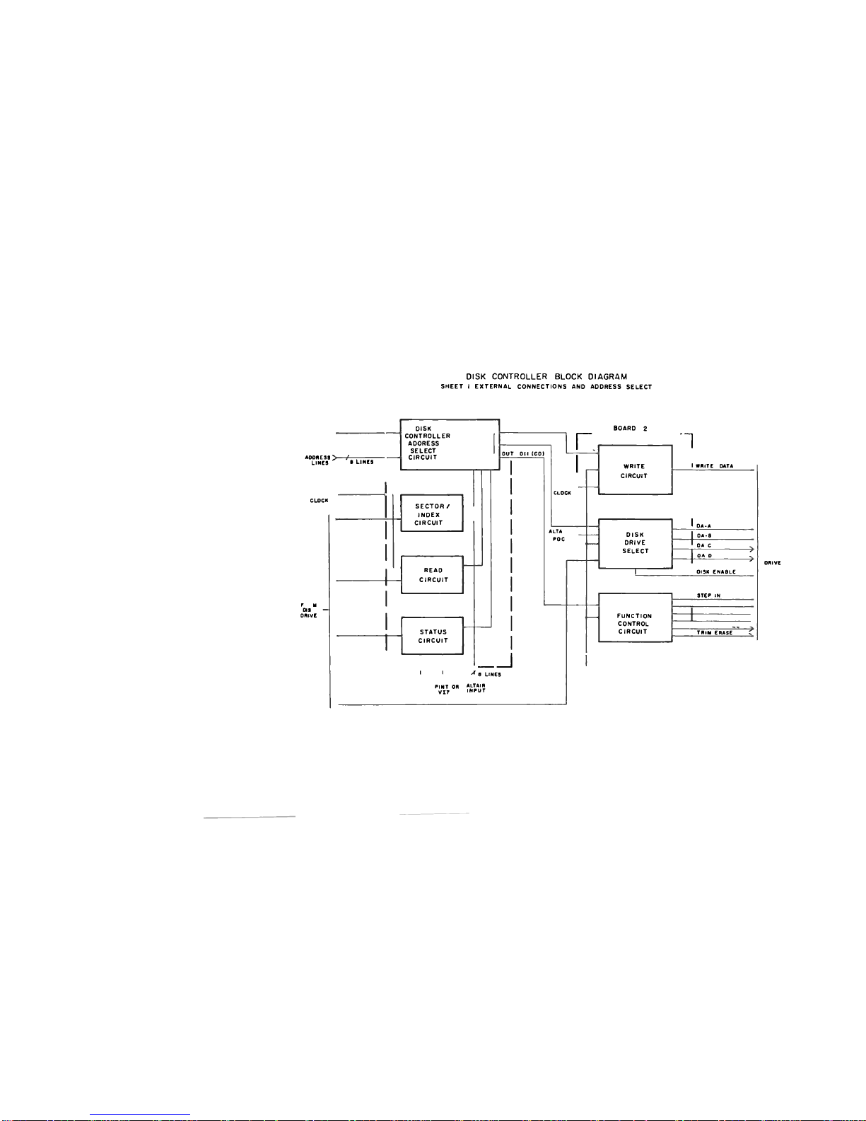
DISK CONTROLLER BLOCK DIAGRAM
SHEET I EXTERNAL CONNECTIONS AND AOORESS SELECT
A00HE99
> /
LIHES < LIWCS
CLOCK
^as" —
ooivt
OISK
CONTROLLER
AOORESS
SELECT
CIRCUIT
READ
CIRCUIT
STATUS
CIRCUIT
SECTOR/
tNOEX
CIRCUIT
ouT on [cot
CLOCK
r
I
[
' ' e LINES
PIMT OH ALTM"
Vt7 IMPUT
ALU
POC
BOARD 2
WRITE
CIRCUIT
1
CIRCUIT
I WHITE MT4
! o*.*
DISK
DRIVE
SELECT
o*.a
DISK
DRIVE
SELECT
o*c ^
DISK
DRIVE
SELECT
0*0 ^
OHK ENA9LE
1
OHK ENA9LE
STEP IX STEP IX
FUNCTION FUNCTION
CONTROL
CIRCUIT
CONTROL
CIRCUIT
TBI* EMSE ?
OHIVE
Page 9
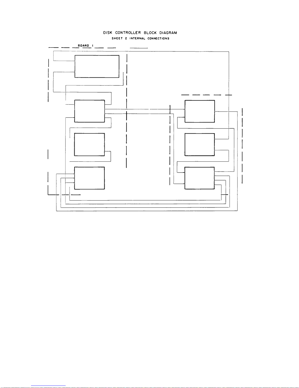
DISK CONTROLLER BLOCK DIAGRAM
SHEET 2 INTERNAL CONNECTIONS
80AR0 I
Page 10

ALTAIR DISK CONTROLLER I/O INFORMATION
A. Address codes for I/O
Address Mode
1.
010
Out Select, latches and enables controller
and disk drive.
010
In
Indicates status of disk drive and controller.
3.
011 Out Controls disk function.
4.
011 In Indicates sector position of disk
5.
012
Out
Write data.
6.
012
In
Read data.
8. Definitions (In order as listed above)
1. Selection of Disk Drive "OUT" on CH #010
D0 LS8 Enables 1 of 16 drives (each drive has a unique ad-
D1 dress, selected by 4 jumper wires) and enables con-
D2 troller (on disk drive buffer P.C. card).
D3 MSB
D4
D5 Not used, don't care.
D6
D7 Clears disk control if set to 1 (D0-D6 don't care).
Disables disk control. Oisk control also cleared
by opening door of disk drive or turning disk drive
power off.
NOTE: a) If disk drive door is open, drive and controller
cannot be enabled.
b) If disk power is off, drive and controller cannot
be enabled.
c) If disk interconnect cable is not connected between
the controller and the drive, drive and controller
cannot be enabled.
Page 11
C) MULIIPLL DISK DRIVE CONNECTION:
1. With multiple Disk Drives, the Disks should have sequential
addresses (i.e., for a .1 drive system you should have Disks
with addresses 0, 1, and 2). They may be connected in any or-
der. There serial # sticker has the Disk Address written on
it. The Disk Address is determined by four jumper wires in
the Disk Buffer P.C. card inside the Drive, and may be changed.
2, Connect the Disks by using the 6 ft. flat cable. Connect the
male connector to the connector marked "From Next Disk" on the
Disk Drive connected to the Controller. The other end of the
cable connects to the next Disk Drive connector marked "To Con-
troller". This procedure is repeated for added Disk Drive.
III. USING THE DISK DRIVE:
A) DISKETTE INFORMATION:
1. Always keep Diskette in envelope when not in use.
2. Keep Diskette away from heat, magnetic fields (flourescent
lights, power transformers, etc.) and dust and dirt.
3. Never touch recording surface of Diskette (opposite label
side).
4. Always mark your Diskette with what is on them. Use adhesive
labels, but don't write on them after they are attached
to the Diskette.
5. The Diskette used is hard Sectored (32 Sector holes, 1 index
hole). Blank Diskettes are available from MITS for $15.00
each. The Diskettes are not IBM compatible.
B) OPERATING THE DISK DRIVE:
1. Open door to Disk Drive by pulling out and down.
2. Insert Diskette into Drive with label side up, making sure
it catches on retaining tab.
3. Close door to Disk Drive.
4. If Disk power is on, wait 10 seconds, after closing door
before activating any programs to access the Disk. Wait
10 seconds after turning power on with Diskette in Drive
before activating any programs to access the Disk. This is
to allow motor speed to stabilize.
5. NEVER: open Disk Drive door or turn power off when Disk Enable
and Head Load lights are on. There would be a good possibili-
ty that you would interrupt the software during a write func-
tion, and destroy data on the Diskette.
6. Consult software documentation on methods used to load basic or
use software. For applications where the user wishes to
write his own software. See last section, "Controller I/O
Information".
Page 12

2. Status (010 - INP) indicates disk status when drive and controller
enabled. Also gives valid "INTE" status (05) from the ALTAIR bus
when controller enabled.
True condition = 0, False = 1.
All false if disk and controller are not enabled, and all false if
no disk in drive.
D0 - ENWO - Enter new Write data - indicates write circuit is ready
for new data byte to be written. It occurs every 32 us and
starts 280 ps after sector true (when Write enabled). It is
reset by outputting to the Write data channel (012).
Dl - Move Head - Indicates head movement allowed when true (step
IN, step OUT,). Goes false for 10 ms, true 1 ms, false 20
ms after step command. May step every 10 ms. Goes false for
40 ms after head load. Goes false during Write and 475 us
after Write to allow completion of trim erase.
D2 - HS - Head Status - True 40 ms after head loaded or step command
Ii*f stepping with head already loaded). Indicates when head
is properly loaded for reading and writing. Also enables sec-
tor position channel when true.
03 - Not Used, = 0.
D4 - Not Used, = 0.
D5 - INTE - Indicates interrupt enabled.
D6 - TRACK 0 - Indicates when head is on outermost track.
D7 - NROA - New read data available - indicates that the read cir-
cuit has 1 byte of data ready to be taken from the read data
channel (012). After the SYNC* bit is detected, it occurs
every 32 ps and is reset by an input instruction on channel
012. The byte containing the SYNC bit is the first byte
read from the disk.
* See "Write Enable"
Page 13

Control (011 - Out) - Controls Disk operations when disk drive
and controller enabled. A true signal, logic 1, on a data line
will control the disk as follows:
00 - Step IN - steps disk head in one position to higher numbered
track.
D1 - Step OUT - steps disk head out one position to lower numbered
track.
D2 - Head Load - loads head onto disk - enables sector position
status.
D3 - Head Unload - removes head from disk surface, may be unloaded
immediately after "Write Enable" (write and trim erase circuits
hold head loaded until through).
D4 - ^E - Interrupt Enable - enables interrupts to occur when SR0
true (see sector definition).
D5 - H) - Interrupt Disable - disables interrupt circuit. Interrupt
circuit also disabled by clearing disk control.
D6 - HCS - Head Current Switch - must be true when outputting a write
instruction with the head on tracks 43-76. This reduces head
current and optimizes resolution on inner tracks (automatically
reset at end of writing a sector).
D7 - Write Enable - initiates write sequence as follows:
1. Disk selected and enabled, head loaded, enabling sector status.
2. (Sector True) detected for desired sector, write circuit
enabled by software.
3. 200 us from Write Enable, trim erase automatically turned
on. 280 us from start of sector, "ENWD" goes true, sync
byte written by software.
4. First byte written always has most significant (D7) bit A
"1" (SYNC Bit) (most sifnificant bit written first).
5. ENWD goes true every 32 us. MAX. no. of data bytes per
sector 137 (including SYNC).
6. Last or 138th byte written must be a 000. This will be
written for the remainder of the sector. Ignore "ENWD"
from this point to end of sector.
7. At end of sector, the write circuit automatically disabled,
trim erase disabled 475 us later.
Page 14

NOTE: a) Write circuit will continue writing last byte out-
putted on CH #012 to the end of that sector.
b) Head may be unloaded anytime during write cyclr it* no
read or write function is cxpcctcd after current write
cycle. Once Write is enabled, it holds the head loaded
for the required time. (For writing and trim erase).
4. Sector Position (011 - INP) with disk drive and controller enabled,
and 40 ms after head is loaded, the sector information is as follows
00 - SR0 - Sector True - True when = 0, and is 30 ps long. The
write mode should begin as close as possible to the time that D0
goes true. Write data will be requested 280 ps after D0 goes
true. Read data will be available 140 ps after SR0 goes true.
SECTOR #
0
1
2 3
31
U1-SR1-
0
1
0
1
1
D2-SR2-
0 0
1 1
1
D3-SR3-
0 0 0
0
1
D4-SR4-
0
0 0
0
1
D5-SR5-
0 0 0 0
1
b. Write Data (012-OUT) Outputted on the "ENWD" status request.
6. Read Data (012-IN) Inputted on the "NRDA" status flag.
Page 15
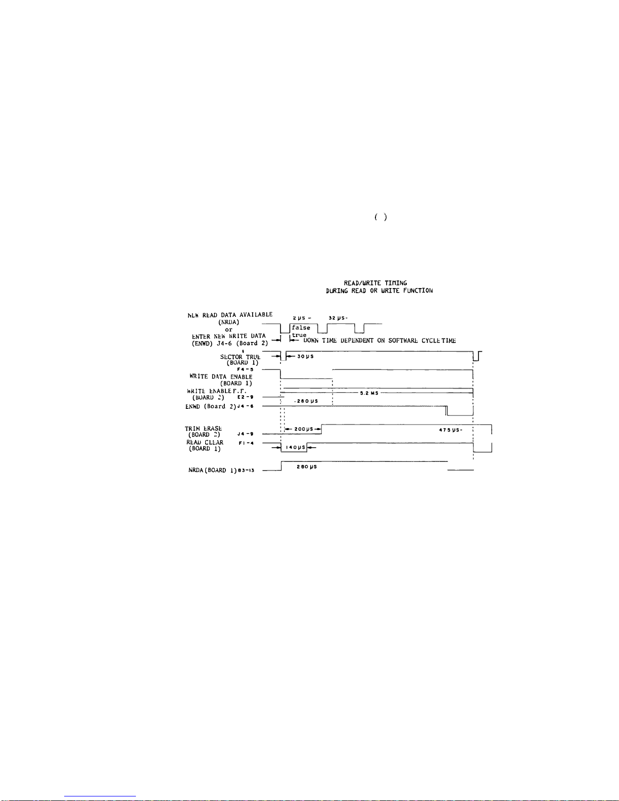
( )
READ/URITE TIMING
DURING READ OR URITE FUNCTION
NLh READ DATA AVAILABLE
(NRDA) ) r^
or
[_]
false
ENTER NEh URtTE DATA
(ENWD) J4-6 (Board 2)
SECTOR* TRUE -^J— soVs
(BOARD 1) .
F4 - S
WHITE DATA ENABLE
(BOARD 1)
WRITE EhABLEF.r.
(BOARD 2) E2
- 9
EKhD (Board 2)^-6
32 ps-
] itrue
—J k- DOWN TIME DEPENDENT ON SOFTWARE CYCLE TIML
TRIM ERASE
(BOARD :)
READ CLEAR
(BOARD 1)
Jl -9
F!
-4
.
2SO
tJS
j—-
200 tJS-*-
—-j ! 40)JS ——
If
5.2 MS
47 5 PS-
NRDA(BOARD l)a:-n
2ao ps
Page 16

*********** ERRATA SHEET ***********
ALTAIR FLOPPY DISK
DRIVE & CONTROLLER - HARDWARE DOCUMENTATION
March 1976
THE FOLLOWING CHANGES HAVE BEEN MADE TO THE ABOVE
TITLED MANUAL ON THE PAGES INDICATED.
PAGE 32: No heat-sink should be used for either XI or X3. Mount both
of these regulators directly to the board.
PAGE 95: Use a length of wire and connect the two pads labeled +8V to-
gether along the bottom edge of the board.
IT IS GENERALLY A GOOD IDEA TO GO THROUGH
YOUR MANUAL AMD MARK THESE CHANGES ON THE
PAGES INDICATED BEFORE BEGINNING THE ACTUAL
PROCESS OF ASSEMBLING YOUR UNIT.
HITS, Inc.
3/16/76
Page 17

^k ccntro^er assembly procedure
Page 18

ASSEMBLY H!MT$
Before beginning the construction of your unit, it is important that you read
the "M!TS Kits Assembly Hints" booklet included with your kit. Pay particular
attention to the section on soldering, because most problems in the Altair
occur as the result of poor soldering. It is essential that you use the cor-
rect type of soldering iron. A 25-30 watt iron with a chisel tip (such as an
Ungar 776 with a 7155 tip) is recommended in the assembly hints booklet.
Some important warnings are also included in the hints booklet. Read them
carefully before you begin work on your unit -- failure to heed these warnings
could cause you to void your warranty.
Check the contents of your kit against the enclosed parts list to make sure
you have all the required components, hardware and parts. The components are
in plastic envelopes; do not open them until you need the components for an
assembly step. You will need the tools called for in the "Kits Assembly
Hints" booklet.
As you construct your kit, follow the instructions in the order they are
presented in the assembly manual. Always complete each section before going
on to the next. Two organizational aids are provided throughout the manual
to assist you: 1) Boxed-off parts identification lists, with spaces provided
to check off the components as they are installed; 2) Reproductions of the
silk screens showing a) previously installed components, b) components being
installed and c) components yet to be installed, (see below)
previously
installed
components
components
yet to be
installed
components
bei
ng
installed
-un inE
Page 19

COMPONENT INSTALLATION METHODS
This section of the manual describes the proper pro-
cedures for installing various types of components
in your kit.
Read these instructions over very carefully and
refer back to than whenever necessary. Failure to
properly install components may cause permanent
damage to the component or the rest of the unit;
it will definitely void your warranty.
More specific instructions, or procedures of a
less general nature, will be included within the
assembly text itself.
Under no circumstances should you proceed with an
assembly step without fully understanding the pro-
cedures involved. A little patience at this stage
will save a great deal of time and potential "head-
aches" later.
2
Page 20
PIM t
u
o
PIN I
rr
PIN I
°o
o
PIM I
INTEGRATED CIRCUITS (IC's) CAN COME WITH ANY ONE OF, OR A COMBINATION
OF, SEVERAL DIFFERENT MARKINGS. THESE MARKINGS ARE VERY IMPORTANT IN
DETERMINING THE CORRECT ORIENTATION FOR THE IC's WHEN THEY ARE PLACED
ON THE PRINTED CIRCUIT BOARDS. REFER TO THE ABOVE DRAWING TO LOCATE
PIN 1 OF THE IC's, THEN USE THIS INFORMATION IN CONJUNCTION WITH THE
INFORMATION BELOW TO PROPERLY ORIENT EACH IC FOR INSTALLATION.
j WARNINGl INCORRECTLY ORIENTED IC's MAY CAUSE PERMANENT DAMAGE!
L
E C E
B
THE DRAWING ON THE LEFT INDICATES VARIOUS
METHODS USED TO SHOW THE POSITION OF IC's
ON THE PRINTED CIRCUIT BOARDS. THESE ARE
SILK-SCREENED DIRECTLY ON THE BOARD. THE
ARROWHEAD INDICATES THE POSITION FOR PIN 1
WHEN THE IC IS INSTALLED.
3
Page 21
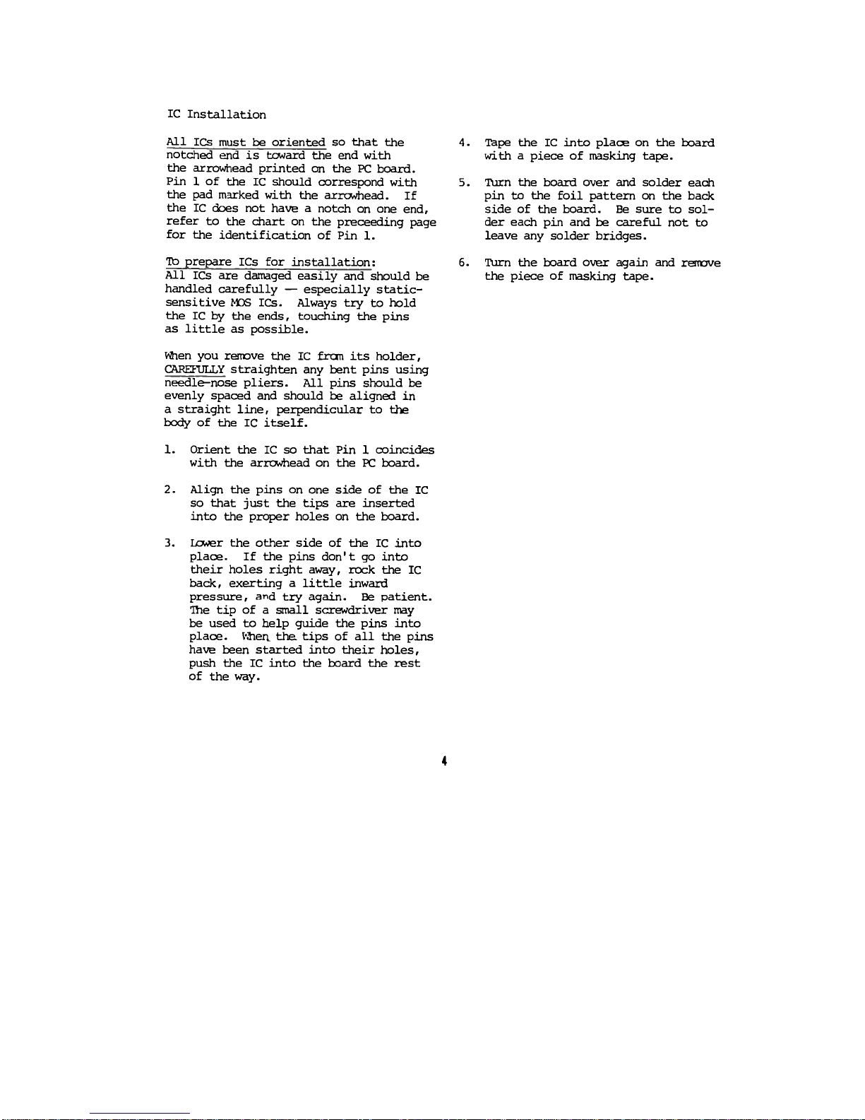
IC Installation
All ICS must be oriented so that the
notched end is toward the end with
the arrowhead printed on the PC board.
Pin 1 of the IC should correspond with
the pad marked with the arrowhead. If
the IC does not have a notch on one end,
refer to the chart on the proceeding page
for the identification of Pin 1.
lb prepare ICs for installation:
All ICs are damaged easily and should be
handled carefully — especially static-
sensitive MOS ICs. Always try to hold
the IC by the ends, touching the pins
as little as possible.
Mien you remove the IC fran its holder,
CAREFULLY straighten any bent pins using
needle-nose pliers. All pins should be
evenly spaced and should be aligned in
a straight line, perpendicular to the
body of the IC itself.
1. Orient the IC so that Pin 1 coincides
with the arrowhead on the PC board.
4. Tape the IC into place on the board
with a piece of masking tape.
5. Turn the board over and solder each
pin to the foil pattern on the back
side of the board. Be sure to sol-
der each pin and be careful not to
leave any solder bridges.
6. Turn the board over again and remove
the piece of masking tape.
2. Align the pins on one side of the IC
so that just the tips are inserted
into the proper holes on the board.
3. Lcwer the other side of the IC into
place. If the pins don't go into
their holes right away, rock the IC
back, exerting a little inward
pressure, and try again. Be patient.
The tip of a small screwdriver may
be used to help guide the pins into
place.
S-3ien the.
tips of all the pins
have been started into their holes,
push the IC into the board the rest
of the way.
4
Page 22
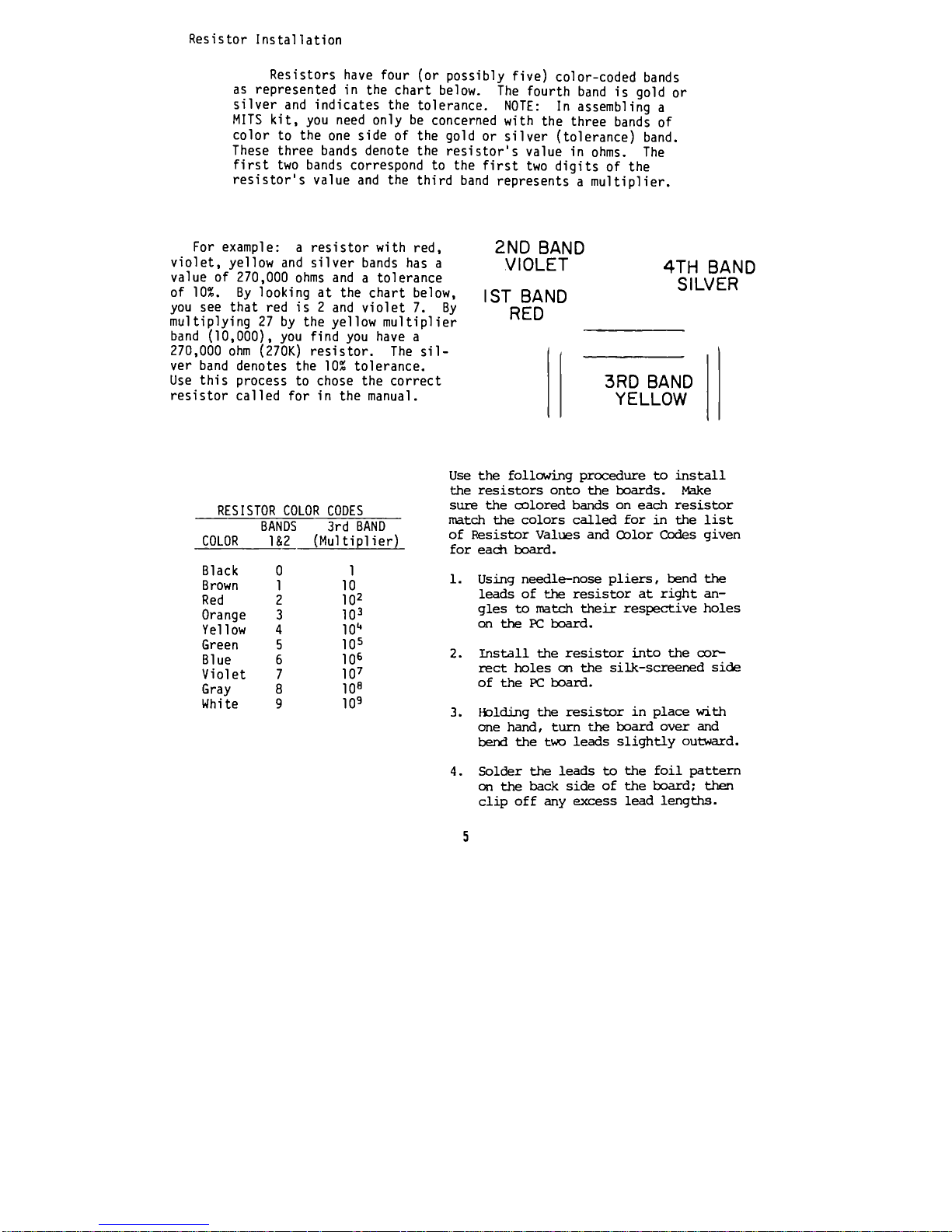
Resistor installation
Resistors have four (or possibly five) color-coded bands
as represented in the chart below. The fourth band is gold or
silver and indicates the tolerance. NOTE: In assembling a
MITS kit, you need only be concerned with the three bands of
color to the one side of the gold or silver (tolerance) band.
These three bands denote the resistor's value in ohms. The
first two bands correspond to the first two digits of the
resistor's value and the third band represents a multiplier.
For example: a resistor with red,
violet, yellow and silver bands has a
value of 270,000 ohms and a tolerance
of 10%. By looking at the chart below,
you see that red is 2 and violet 7. By
multiplying 27 by the yellow multiplier
band (10,000), you find you have a
270,000 ohm (270K) resistor. The sil-
ver band denotes the 10% tolerance.
Use this process to chose the correct
resistor called for in the manual.
2ND BAND
VIOLET
1ST BAND
RED
4TH BAND
SiLVER
3RD BAND
YELLOW
RESISTOR COLOR CODES
BANDS
3rd BAND
COLOR
1&2
(Multiplier)
Black
0 1
Brown
1
10
Red
2
10^
Orange
3
10^
Yellow
4 10"
Green 5
105
Blue
6
106
Violet 7 10?
Gray 8
10S
White 9
109
Use the following procedure to install
the resistors onto the boards. Make
sure the colored bands on each resistor
match the colors called for in the list
of Resistor Values and Color Codes given
for each board.
1. Using needle-nose pliers, bend the
leads of the resistor at right an-
gles to match their respective holes
on the PC board.
2. Install the resistor into the cor-
rect holes en the silk-screened side
of the PC board.
3. Holding the resistor in place with
one hand, turn the board over and
bend the two leads slightly outward.
4. Solder the leads to the foil pattern
on the back side of the board; then
clip off any excess lead lengths.
5
Page 23
Capacitor Installation
A. Electrolytic and Tantalun Capacitors
Polarity requirements must be noted on
the electrolytic capacitors and the tan-
talum capacitor before they are installed.
The electrolytic capacitors contained in
your kit may- have one or possibly two of
three types of polarity markings, lb
determine the correct orientation, look
for the following.
One type will have plus (+) signs on the
positive end; another will have a band
or a groove around the positive side in
addition to the plus signs. The third
type will have an arrw on it; in the tip
of the arrow there is a negative
(-)
sign
and the capacitor must be oriented so the
arrow points to the negative polarity side
The tantalum capacitor is metallic in
appearance and smaller than the elec-
trolytic capacitors. Its positive end
has a plus sign on it or a red dot.
Refer to the chart included for each
board for correct Capacitor Values and
install the electrolytic capacitors and
tantalum capacitors using the following
procedure.
1. Bend the two leads of the capacitor
at right angles to match their re-
spective holes on the board. Insert
the capacitor into the holes on the
silk-screened side of the board. Be
sure to align the positive polarity
side with the "+" signs printed on
the board.
2. Holding the capacitor in place, tum
the board over and bend the two
leads slightly outward. Solder the
leads to the foil pattern and clip
off any excess lead lengths.
B. Ceramic Disk Capacitors
Refer to the chart included for each
board for correct Capacitor Values, and
install the ceramic disk capacitors using
the following procedure.
1. Choose the correct value capacitor
and straighten the two leads as
necessary to fit their respective
holes on the PC board.
2. Insert the capacitor into the cor-
rect holes fron the silk-screened
side of the board. Push the capaci-
tor dwn until the ceramic insula-
tion almost touches the foil pattern.
3. Holding the capacitor in place, tutrn
the board over and bend the two leads
slightly outward.
4. Solder the two leads to the foil
pattern on the back side of the
board; then clip off any excess lead
lengths.
Page 24
Transistor Installation
Diode Installation
lb install transistors, use the foll-
owing instructions.
NOTE: Always check the part number of
each transistor before you install it.
(See listing of Transistor Part Numbers
for each board.) Sane transistors look
identical but differ in electrical char-
acteristics, according to part number.
If you have received substitute part
numbers for the transistors in you kit,
check the Transistor Identification
Chart which follows these instructions
to be sure you make the correct sub-
stitutions.
NOTE: Always make sure the transistor
is oriented so that the emitter lead is
installed in the hole on the PC board
labeled with an "E." lb determine
which lead is the emitter lead, refer to
the Transistor Identification Chart.
1. After the correct transistor has
been selected and the leads have
been properly oriented, insert the
transistor into the holes on the
silk-screened side of the board.
2. Holding the transistor in place,
tum the board over and bend the
three leads slightly outward.
NOTE: Diodes are marked with a band on
one end indicating the cathode end.
Each diode must be installed so that
the end with the band is oriented towards
the band printed on the PC board. Fail-
ure to orient the diodes oorrectly may
result in permanent damage to your unit.
Use the following prooedure to install
diodes onto the board. Refer to the list
of Diode Part Numbers included for each
board to make sure you install the correct
diode each time.
1. Bend the leads of the diode at right
angles to match their respective
holes on the board.
2. Insert the diode into the correct
holes on the silk screen, making
sure the cathode end is properly
oriented. Tum the board over and
bend the leads slightly outward.
3. Solder the two leads to the foil
pattern on the back side of the
board; then clip off any excess
lead lengths.
3. Solder the leads to the foil pattern
on the back side of the board; then
clip off any excess lead lengths.
7
Page 25
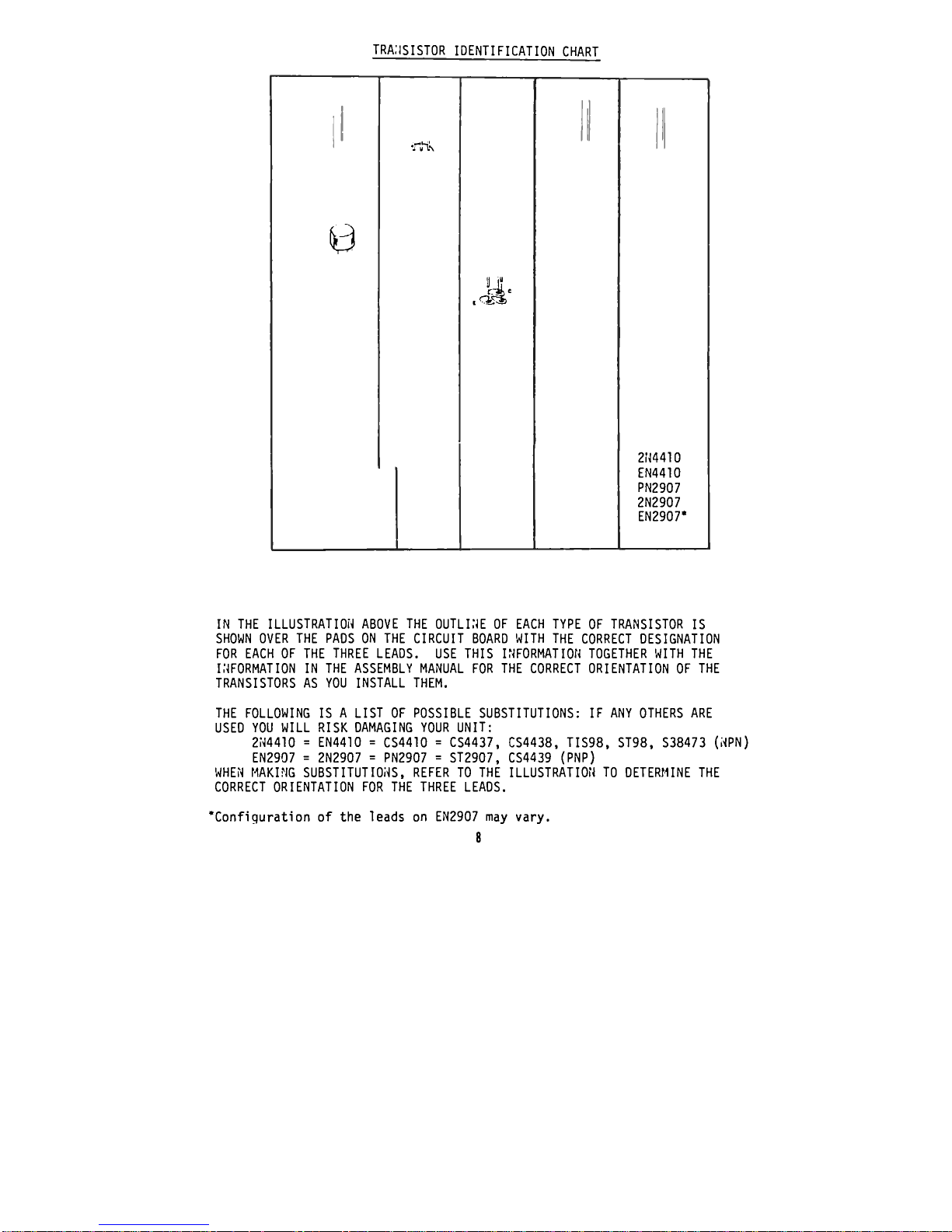
TRA.'iSISTOR IDENTIFICATION CHART
0
-rh-.
.A
2N4410
EN4410
PN2907
2N2907
EN2907*
IN THE ILLUSTRATION ABOVE THE OUTLINE OF EACH TYPE OF TRANSISTOR IS
SHOWN OVER THE PADS ON THE CIRCUIT BOARD WITH THE CORRECT DESIGNATION
FOR EACH OF THE THREE LEADS. USE THIS INFORMATION TOGETHER WITH THE
INFORMATION IN THE ASSEMBLY MANUAL FOR THE CORRECT ORIENTATION OF THE
TRANSISTORS AS YOU INSTALL THEM.
THE FOLLOWING IS A LIST OF POSSIBLE SUBSTITUTIONS: IF ANY OTHERS ARE
USED YOU WILL RISK DAMAGING YOUR UNIT:
2N4410 = EN4410 = CS4410 = CS4437, CS4438, TIS98, ST98, S38473 (NPN)
EN2907 = 2N2907 = PN2907 = ST2907, CS4439 (PNP)
WHEN MAKING SUBSTITUTIONS, REFER TO THE ILLUSTRATION TO DETERMINE THE
CORRECT ORIENTATION FOR THE THREE LEADS.
'Configuration of the leads on EN2907 may vary.
8
Page 26
disk drive assembly procedure
Page 27

t'A.'iK T<)t' M-:W;VAL
Remove the top from the Disk Drive case
by withdrawing the two screws indicated
in the drawing below. Slide the case
top backwards, lifting the back slightly,
to remove it entirely from the chassis.
Also remove the 4 screws in the side of
the case bottom, and remove the entire
chassis assembly.
Page 28

DISK DRIVE BACK PANEL ASSEMBLY
Remove the back panel from the case by
withdrawing each of the four screws in
the comers of the panel. These four
screws are shown inserted in the draw-
ing below.
Save these four screws for remounting
the back panel later in the assembly
procedure.
Page 29

Terminal Block Installation
Mount the terminal block to the back panel
as shown in the drawing below. Use the
screw sizes and other hardware indicated
in the drawing.
NOTE: Be sure that the back panel is
oriented as shown; be careful
not to mount the terminal block
on the wrong side of the panel.
Tighten all four screws firmly into place.
13
Page 30
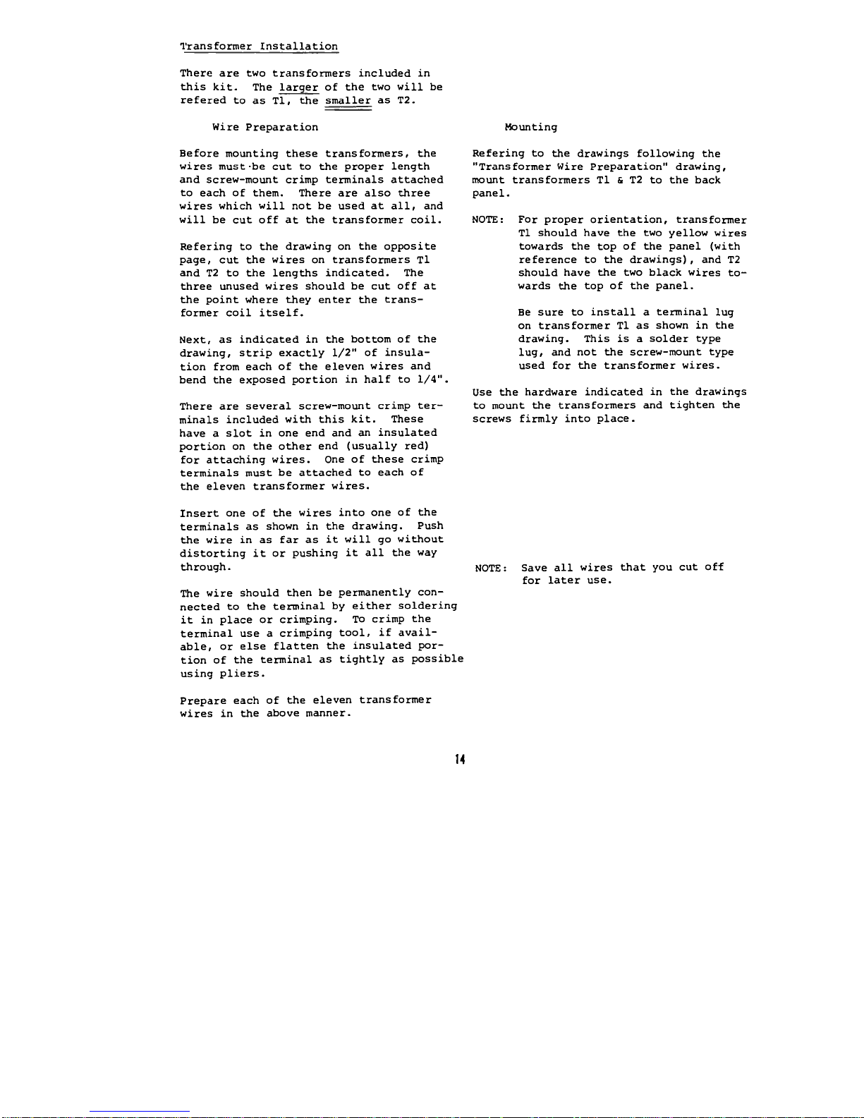
Transformer Installation
There are two transformers included in
this kit. The larger of the two will be
refered to as Tl, the smaller as T2.
Wire Preparation
Before mounting these transformers, the
wires must-be cut to the proper length
and screw-mount crimp terminals attached
to each of them. There are also three
wires which will not be used at all, and
will be cut off at the transformer coil.
Refering to the drawing on the opposite
page, cut the wires on transformers Tl
and T2 to the lengths indicated. The
three unused wires should be cut off at
the point where they enter the trans-
former coil itself.
Next, as indicated in the bottom of the
drawing, strip exactly 1/2" of insula-
tion from each of the eleven wires and
bend the exposed portion in half to 1/4".
There are several screw-mount crimp ter-
minals included with this kit. These
have a slot in one end and an insulated
portion on the other end (usually red)
for attaching wires. One of these crimp
terminals must be attached to each of
the eleven transformer wires.
Mounting
Refering to the drawings following the
"Transformer Wire Preparation" drawing,
mount transformers Tl & T2 to the back
panel.
NOTE: For proper orientation, transformer
Tl should have the two yellow wires
towards the top of the panel (with
reference to the drawings), and T2
should have the two black wires to-
wards the top of the panel.
Be sure to install a terminal lug
on transformer Tl as shown in the
drawing. This is a solder type
lug, and not the screw-mount type
used for the transformer wires.
Use the hardware indicated in the drawings
to mount the transformers and tighten the
screws firmly into place.
Insert one of the wires into one of the
terminals as shown in the drawing. Push
the wire in as far as it will go without
distorting it or pushing it all the way
through. NOTE: Save all wires that you cut oM
for later use.
The wire should then be permanently con-
nected to the terminal by either soldering
it in place or crimping. To crimp the
terminal use a crimping tool, if avail-
able, or else flatten the insulated por-
tion of the terminal as tightly as possible
using pliers.
Prepare each of the eleven transformer
wires in the above manner.
14
Page 31

cut off
YELLOW/GREEN
TRANSFORMER WIRE PREPARATION
STRIP
r i
BEND
^
TERMINAL
!5
Page 32

16
Page 33

Fuse Holder Installation
Refering to the drawing below, mount the
fuse holder to the back panel using the
rubber washer and nut provided. Tighten
it firmly into place.
Remove the cap and place the fuse provided
with your kit into the holder, then replace
the cap.
BACK PANEL
RUBBER
WASHER
NUT
17
Page 34

90° ANGLE CLIP INSTALLATION
The drawing below illustrates the hard-
ware and orientation for mounting the
90° angle clip included with this kit.
NOTE: One side of the clip is slightly
shorter than the other. The
shorter side should be mounted
against the back panel with the
longer side extending at 90°.
Install the clip as shown below and tighten
the screws firmly into place. Be sure that
clip remains "square" with the panel when
tightening the screws.
Page 35

Fan Installation
before the cooling fan is installed onto
the back panel, two lengths of wire must
be prepared and connected to it.
There is some black wire included with
the kit; cut two 6 1/2 inch lengths of
this wire. Strip 1/2 inch of insulation
from one end of each of the wires, and
1/4 inch of insulation from the other.
In the same manner as described on page
, attach a screw-mount crimp terminal
to the 1/2" stripped end of each of the
two wires. Tin the 1/4" stripped ends
of the wires by applying a thin coat of
solder.
There are two terminals on the fan in one
of the comers. Solder the ends of the
two wires opposite the crimp terminals to
the terminals on the fan.
Refering to the drawing below, mount the
fan and screen to the back panel using
the hardware indicated. For proper
orientation, the terminals with the two
wires attached should be towards the
bottom on the side nearest the terminal
block. The arrow printed on the fan
to indicate airflow should be facing
towards the screen. The screen itself
has a bump on one side in each of the
four comers. The side with the bumps
should be towards the fan.
(4)^6-32 X 2" FLATHEAD
SCREWS
4) CLIP-ON NUTS
PROTECTIVE
SCREEN
(4)*6 FLATWASHERS
(4)*6 LOCKWASHERS
(4)*6 32 NUTS
19
Page 36

Power Cord Installation
There is a 3-wire power cord included with
this kit which must be prepared as follows
before installation.
1) Strip 4" of the cord casing from the
wires by cutting a circle 4" from the
end and pulling off the black insula-
tion. Be careful not to cut into the
insulation on any of the wires inside.
2) The green wire inside should already
be at the correct length of 4 inches.
Cut the white wire to 3 1/2 inches,
and the black wire to 1 1/4 inches.
Strip 1/4 inch of insulation from the
ends of each of the three wires.
Place the strain relief, included with
the kit, over the power cord. Be sure
that the larger diameter end of the
relief is towards the male plug end of
the cord.
Be sure that there is approximately three
inches of the cord's black insulation
case extending beyond the strain relief*,
then snap it into place on the back panel
as shown below.
* The black wire should reach to the
center of the fuse holder when the
cord & strain relief are in place.
3) Tin the exposed 1/4" of the black
wire by applying a thin coat of
solder.
4) Solder or crimp screw-mount crimp
terminals to the white and green
wires.
20
Page 37

Wtru Preparation
Using the wire supplied with this kit,
and the length of yellow/green wire cut
from transformer Tl, prepare the power
supply interconnect wires according to
the following instructions.
Interconnect Wires
To
avoid confusion, it would be best to
COLOR
LENGTH TAG
prepare these wires one at a time.
Yellow/
2 inches 3
The list on the right indicates the color
Green*
of each wire, the length to which it
should be cut, and a reference "tag".
Black
22 3/4
3
Use the following steps to prepare each Black
17 3/4
9
wire:
Black
17 1/2
10
1)
Cut the specified color wire to the
length indicated.
Black 25
1
2)
Strip 1/2 inch of insulation from
White 18 6
one end and 1/4 inch from the other.
White
17 3/4
8
3) Tin the wire exposed 1/4 inch by ap-
plying a thin coat of solder.
Orange
17 3/4
7
4)
According to the instructions on
Orange
18 1/2
4
page , connect a screw-mount
crimp terminal to the 1/2 inch
Orange
18 1/4
5
stripped end.
5)
Approximately 5 inches from the 1/4
*From transformer Tl,
inch tinned end of the wire label it,
This
wire need not be
using masking tape, with the refer-
labeled.
ence tag indicated.
An additional length of BLACK wire should
be cut to 22 1/2 inches and 1/4 inch of
insulation stripped from each end. Tin
both ends by applying a thin coat of solder.
Label this wire "FUSE".
2)
Page 38

Back Panel Wiring
The disk back panel assembly may now be
completed by connecting all of the wires
to their appropriate locations.
[See drawing page 2 3)
Three solder connections are necessary
and should be made first. These in-
clude the black power cord wire, the
yellow/green wire and the black 22 1/2
inch wire labeled "FUSE".
1) Solder the 1/4 inch tinned end of the
yellow/green wire to the solder lug
on transformer Tl.
2) Solder the black power cord wire to
the center terminal on the fuse
holder.
3) Solder one end of the black "FUSE"
wire to the other fuse holder ter-
minal.
The remaining connections will be made to
the terminal block.
The drawing(P.23) shows the proper orienta-
tion and connections for all of the wires
on the back panel. The "tags" on the wires
you prepared earlier refer to the numbers
shown on the terminal block.
WARNING: The power supply is a critical
part of any electronic system.
Check the wiring here several
times to be sure you have it
correct. Be sure that each of
the wires is in the proper loca-
tion and that all of the screws
on the terminal block are tight.
Use the drawing below for reference and
connect all of the wires as indicated.
Match the "tags" on the wires prepared
earlier with the numbered positions on
the terminal block. There should be
a total of 25 crimp terminal connections
made to the block.
NOTE: Where two terminals are to be con-
nected to the same screw, place
them "back to back". In this posi-
tion they will fit flat together,
and make a much more solid connec-
tion.
The ON-OFF switch may also be soldered in
at this time. Use the free end of the
black "FUSE" wire and the free end of the
wire labeled "1" to connect to the switch
terminals. There are three terminals on
the switch. Use the center terminal and
one to either side of it. (The switch
position towards the side where the con-
nections are made will be its OFF position
Install the 4 tie wraps in the posi-
tions shown in the top drawing on
page 23.
22
Page 39

w[RH Mou'rrm; & tm WRAPS
c
r r
(p
11
W n (P
t:
o)
POWER CORD
0
*TIE WRAPS (4)
AC POWER
CORD
Jll
BACK PANEL WIRING
X
T2
O)
s
OFF ON SW.
23
o
o
o
FAX
Page 40

DISK POWER SUPPLY BOARD ASSEMBLY
NOTE: Save all component leads clipped
off during assembly until the
entire unit is complete. Some
of the leads will be used during
the assembly process.
RESISTOR INSTALLATION
Install the following 2 resistors
according to the instructions listed
on page 5 -
RESISTOR VALUES AND COLOR CODES
( ) R1 is 33 ohm (orange-orange-
black) 1/2 W
( ) R2 is 7.5 ohm, 5 W (this may
be color coded, violet-green-
3rd band white or gold: or it
may be a solid body color, with
the value printed directly on
the resistor itself.
24
Page 41

o !
O
) <
O
o
o
o
o
o
+fo* -y.
! o !
O O O O O O
$ $
f+O
o
o
25
Page 42

CAPACITOR INSTALLATION
CAPACITOR VALUES
Install the following 3 ceramic
disk capacitors according to the
instructions on page 6 .
( ) C2 = .luf, 50V
( ) C5 = .luf, 50V
( ) C8 = .luf, 50V
27
Page 43

CAPACITOR INSTALLATION
Install the following 6 electrolytic
capacitors according to the instruc-
tions listed on page 6 .
CAPACITOR VALUES
J CI = 2200uf, 50V
C3 = 33uf, 50V
Y ) C4 = 3300uf, 16V
\ ) C6 = 33uf, 50V
C7 = lOOOuf, 25V
( ) C9 = 33uf, 50V
43
Page 44

r
M!TS
: o :
D!SK POWER SUPPLY !
R2T
]
C5
<000!
O !
o
C8
C! ) + C3) +
t <
D!
OOOOO
29
o
Page 45

DIODE INSTALLATION
Install the following 2 diodes
according to the instructions
on page 7 -
( ) D1 = 1N4004
( ) D2 = 1N4004
+33"'13
O ;
tO.__Qj
D)
$ 9'
o
o !
-Qi
o o o o o o
3)
Page 46

VOLTAGE REGULATOR INSTALLATION
There are 2 voltage regulators to be
installed on the silk-screened side of
the power supply board, XI & X3.
These are to be installed according
to the following procedure. (see
drawing-right)
(1) Set the regulator in place
over the board so that the
mounting hole in the regu-
lator and the board align.
(2) Use a pencil to mark the point
on each of the regulator's
three leads directly over
its corresponding hole in the
board.
(3) Bend the three leads, using
needle-nose pliers, at right
angles from the printed side
of the component.
NOTE: Use heat-sink grease when in-
stalling this component. Apply
it to the surface where the reg-
ulator & board come in contact.
(4) Referring to the drawing, set
the regulator in place on the
silk-screened side of the board.
Secure it to the board using a
#6-32 nut and screw. Hold the
regulator in place as you
tighten the nut to keep from
twisting the leads.
(5) Tum the board over and solder
the three leads to the foil
pattern on the back side of
the board. Be sure not to
leave any solder bridges.
(6) Clip off any excess lead lengths.
the above procedure to install both
of the regulators, XI & X3.
Page 47

VOLTAGE REGULATOR INSTALLATION
( ) XI = 7824
( ) X3 = 7805
MtTS
D)SK POWER
SUPPLY
11.11itiiiimm rnntmn
C4)+
C6)
+
! !
C9l +
O
X3
B
Ct
33
Page 48

BRIDGE RECTIFIER INSTALLATION
There are two bridge rectifiers, BR1
& BR2, to be installed on the power
supply board.
WARNING: Read the following instruc-
tions closely. Proper
orientation of these two
components is absolutely
critical.
These two components are indicated on
the silk-screen by broken lines. This
is to indicate that they are to be
mounted on the bottom (non-silk-
screened) side of the board.
You will observe a "+" sign printed
near one corner of the rectifier.
The lead nearest this "+" sign is
the positive lead of the rectifier.
This lead must be inserted into the -
hole marked on the silk-screen witF
a "+" sign.
NOTE: There is also a "-" sign
printed on the regulator.
The lead nearest this sign is
the negative lead of the recti-
fier, and should be diagonally
opposite the "+" lead on the board.
BE ABSOLUTELY SURE THAT THE PROPER
ORIENTATION IS USED WHEN INSTALLING
THESE TWO COMPONENTS.
Install the rectifiers according to the
following procedure:
(1) Insert the four leads of the
BR1 rectifier into their res-
pective holes from the non-
silk-screened side of the
board. Be sure the "+" lead
of the rectifier is inserted
in the hole labeled "+" on the
silk-screened side of the
board.
(2) Insert the BR2 rectifier in the
same manner. Be sure both recti-
fiers are pushed all the way
against the board.
(3) There is a 90° angle bracket
included with your parts. Each
of the two sides has two holes
in it.
Using the side with the two holes
the furthest apart, set the angle
bracket over the two rectifiers.
The holes in the bracket, the rec-
tifiers, and the board should
align.
Temporarily attach the bracket &
rectifiers to the board through
these holes using #6-32 & 5/8"
screws and nuts.
(4) Check the orientation once more,
then solder all four leads of each
rectifier to the board on the
silk-screened side.
(5) Clip off any excess lead lengths.
Leave the angle bracket in place
for the next procedure.
NOTE: Apply heat-sink compound to
all mating surfaces.
34
Page 49

BRIDGE RECTIFIER INSTALLATION
( ) BR1 = VJ048
( ) BR2 = VJ048
BR2{ O {
'tO___Q!
o
D)
D2
BR)'
"01
o O O O O
O
35
Page 50

DISK BUFFER BOARD
ASSEMBLY
IC INSTALLATION
Install the follow-
ing 7 ICs onto the
Disk Buffer Board
according to the
mathod described on
page 4 .
o
o
o
o
o
o
o
o
IC SILK-SCREEN
DESIGNATIONS AND
PART NUMBERS
( ) A, B, D, & E = 8T97
o
o
o
o
( ) c
= 8198
( ) F
= 74L30
( ) G
= 9601
o
o
o
o
lO
o
o
o
o o
r
<ID-
o
o
o
o
o
o
o
o
o
o
o
o
o
O O
o
O o
o
o
o
o
o
o
o
o
o
o
o
o
o
o
o
o
o
o
o
o
o
o
o °o
o O
o
(1 f)
QO 00
o
00 O
27
Page 51

RESISTOR INSTALLATION
Install
the
following
39
resistors
according
to the
instructions listed
on
page
5 .
RESISTOR VALUES
AND
COLOR CODES
) R9, R7, R5 are 220 ohm
(red-red-brown)
1/2 W
) RIO, R8, R6 are 330 ohm
(orange-orange-brown)
1/2 W
) R12, R14, R16 are 330 ohm
(orange-orange-brown)
1/2 W
) Rll, R13, R15 are 220 ohn
(red-red-brown)
1/2 W
) R33 is 220 ohn
(red-red-brown)
1/2 W
) R34 is 330 ohm
(orange-orange-brcwn)
1/2 W
) R31, R29, R27, R25 are 220 ohn
(red-red-brown)
1/2 W
) R32, R30, R28, R26 are 330 ohn
(orange-orange-brown)
1/2 W
) R36, R35, R37 are 150 ohm
(brown-green-brown)
1/4 W
)
R40 . is /t33iy
ohn
(orang^*orange-brown)
1/2 W
f
(red-red-brown)
1/2 W
) R38 is IX ohm
(brown-black-red)
1/2 W
) R41 is 39K ohn
(orange-v#tite-orange)
1/2 W
) R20, R22, R24 are 330 ohm
(orange-orange-brown)
1/2 W
) R19, R21, R23 are 220 ohm
(red-red-brown)
1/2 W
) R4 & R18 are 330 ohn
(orange-orange-brcwn)
1/2 W
) R3 & R17 are 220 ohn
(red-red-brown)
1/2 W
38
Page 52

!nsert Page
IALTAIR FLOPPY OISKl
Disk Drive Assembly Procedure
Resistor Value Changes, page 38
R39 should be 330 ohms
R40 should be 220 ohms
HITS, Inc.
August, 1976
38*
Page 53

ol
o
o
o
o
o
o
o
o
o o
r
o
o
o
o
o
o
I
o
o
o
o
o
o
o
o
o
o
o
o
o
o
o
0
E
O <=
o o
00*^
o
O
o o
is c
o
00
39
o
00 o
Page 54

DIODE INSTALLATION
Install diode D6 according to the
instructions on page 7 -
( ) D6 = 1N914
o
00 o
54)
Page 55

CAPACITOR INSTALLATION
Capacitor C14 is an electrolytic
capacitor. Capacitors CIO, Cll, C12,
and C13 are ceranic disk capacitors.
Install these ccmponents according
to the instructions listed on page 6 .
CAPACITOR VALUES
( Different voltages may be sub-
stituted in some cases.)
( ) C14 = 500 uf, 25V electrolytic
( ) CIO, Cll, C12 & C13 are .1 uf,
12V ceramic disks.
42
Page 56

o o
o
o
o
o
o
o
o
o
o
o
o
o
o
o
<o
o
o
o
a
o
§r
o
o
o
o
o
o
o
o
o
o
o
o
o
o
o
0
o
o
o
o
o
o
o
o
o
t^t
OD s
o
o
o
e O
c
0
o
o
2. —. "
^Dt
o
o
o
o
o
o
o
o
o
o
o
o
o
o
io
o
o
o
o
o
o
00
43
o
00 O
Page 57

DISK DRIVE RIBBON CABLE ASSEMBLY
Ribbon Cable Preparation
There are three ribbon cable as-
semblies to be prepared for installa-
tion in the disk drive unit. A 12'
length of 18-twisted pairs cable has
been provided for this purpose.
First, cut the 12' length of
cable into two 18-inch lengths and
one 25-inch length. The remainder of
the cable should be saved for later
use.
The following two pages contain
diagrams for the proper lengths and
arrangement for the three cable pieces
you have just cut. The two 18" lengths
will be prepared identically.
The cable sheath itself may be cut
using scissors, and can be stripped by
simply pulling it apart. You will note
that the plastic sheath has "welds" ap-
proximately every inch between the twist-
ed pairs. Try not to make any cuts on
the welds themselves.
Each time a 1/4" of insulation is
stripped from the wires themselves, the
bare ends should be tinned by applying
a thin coat of solder.
Study the diagrams on the next two
pages and prepare the three cable as-
semblies as shown. 3e careful to cut
the wires precisely as indicated, and
do not damage the wire insulation when
cutting the cable sheath.
44
Page 58

18 INCH RIBBON CABLES
18"
14"
CUT TO 2" : STRIP 1/8" & TIN
—j*ir
t t
: i
! i
T
r
rt
2 Pr.
STEP CASING EVENLY
APPROX. EVERY INCH
CUT TO 2"
STRIP 1/4" & TIN
45
Page 59

25 INCH RIBBON CABLE
CUT TO 5" : STRIP 1/2" & TIN
4 PAIR
CUT TO 2" : STRIP 1/4" & TIN
2 PAIR
2 PAIR
2 PAIR
1 PAIR
STEP CASING EVENLY
APPROXIMATELY 1 1/2"
STEPS
CUT TO 2 1/4"
STRIP 1/4" & TIN
7
46
Page 60

There arc several 37-pin connectors in
tins kit. One male conncctor and one
temalc conncctor will be used now to
connect onto one end of each of the two
18 inch lengths of ribbon cable that
you have just prepared. The other end
of the two cables will connect directly
to the Disk Buffer board.
Connector Preparation
The two 37-pin connectors must first be
prepared for attaching to the cables.
It may be helpful to solidly mount the
connectors to some steady object dur-
ing this and the following procedures.
1) Place the connector in front of
you with the hollow solder pins
facing upwards.
You will note that the pins on the 37-pin
connectors are all numbered. Note also
that the numbers on the male connector
are the reverse of the female. The male
connector will be wired to the rows of 1
pads on the buffer board labeled "TO"^—^
The female connector will be wired to
the rows of pads labeT^^"FROM". The
numbers on the connector pins corre-
spond directly with the numbers that
label the pads on the buffer board.
2) Using your soldering iron, very
carefully heat each pin one at a
time and fill the hollow space
with solder. The solder should
not quite fill the pin and should
have a slightly concave surface.
Prepare all 37 pins on one male and one
female connector in this manner. Be
sure not to leave any solder bridges
between the pins, and be careful not
to melt any of the nylon insulation
around them.
WARNING
During the following procedure, and
later steps involving ribbon cable,
be sure that you fully understand
all of the instructions before you
begin. These points are the most
likely areas for assembly errors to
occur.
Cable Assembly
The following procedure should be used
for assembling both of the 18 inch
cables. In order to minimize the pos-
sibility of error, the cables will be
attached to the 37-pin connectors and
the Disk Buffer board during the same
procedure. Read this entire procedure
over carefully before beginning.
The following pages contain drawings of
both the 37-pin connectors, and the Disk
Buffer board silk-screen. There is a
space provided to "check-off" each of
the twisted-pair wires as they are con-
nected. Double arrows are also shown
to indicate the connection points for
each of the twisted-pairs.
Orient one of the 18 inch cables so that
the "stepped" edge of the cable casing
is along the rows of pads on the buffer
board labeled "TO". The longest wires
should be near the pads labeled "19 & 37"
and the shortest wires near the pads
labeled "1 & 20". Place the MALE 37-pin
connector near the other end of the
cable.
Begin with the shortest twisted-pair of
wires, nearest the outside edge of the
cable casing, on the buffer board end.
Separate the two wires slightly, then
solder them into the two pads labeled
"1 & 20" on the buffer board. Do this
by inserting the wires from the silk-
screened side of the board and solder-
ing them on the back. Be careful not
to push any of the wire insulation
into the holes. Clip off any excess
wire from the connections and then
check-off the appropriate space on the
silk-screen drawing.
47
Page 61

The same twisted-pair of wires should
now be connected to the pins numbered
"1 & 20" on the 37-pin connector.
Observe the color of the wire now con-
nected to the pad on the buffer board
labeled "1". Be sure to connect this
same wire to the pin numbered "1" on
the connector. Do the same with pad
"20" and pin "20".
Make the connections by re-melting the
solder in the pins and inserting the
-
wires up to their insulation. Remove
the heat from the pins while still
holding the wires in place until the
solder cools. Check-off the appropri-
ate space on ':he connector drawing.
Move to the next twisted-pair of wires
in the ribbon cable and use the same
procedure to connect pads "2 & 21" with
pins "2 & 21". Continue in this manner,
moving across the ribbon cable one pair
at a time, until all 18 twisted-pairs
are in place. Be sure that you do not
connect any wires to pin "12" on the
connector.
NOTE: Take your time and be careful
while soldering the wires to
the connectors. Do not melt
any of the wire insulation or
leave any solder bridges.
Check your work as you go along
and be sure that 1 is connected
to 1, 2 to 2, 3 to 3, etc., be-
cause corrections will be very
difficult later.
Use this procedure to assemble both of
the 18 inch cables. Be sure that the
MALE 37-pin connector goes to the pads
labeled "TO" and the FEMALE connector
to the pads labeled "FROM". Refer to
the drawing on page to get a rough
idea of how these and the next cable
will appear when connected to the board.
( )
( )
Y
"Y
V
)
v
V
fl
-O 20
—O
-o
-<5
—o
Bsaas<
-o
—o
-O 22
-o
-O 23
-o
-O 24
—o
-O 27
-o
IT
9
-O 2.
—o
10
-O 2.
—o
I)
-O ,0
13
-o
3
6
14
-O ,2
—o
15
-O 33
—O
16
-O 34
-^o
)7
-O 3 =
-^O
IS
-lO
-036
-O"
Page 62

37-PIN MALE CONNECTOR
PIN 12 NOT USED
49
Page 63

o
—o
—o
:
-o
-o
50
Page 64

37-PIN FEMALE CONNECTOR
PIN 12 NOT USEO
51
Page 65

Due to it:; complexity, the inch length
of ribbon cablc will be assembled in a
slightly different manner.
The following two pages contain drawings
of one end of -the ribbon cable and the
44-pm edge connector included with this
kit. These connections, on one end of
the ribbon cable only, will be made first.
NOTE: Be sure to observe that
the orientation of the
edge connector is not the
same in all of the drawings.
Use the pin designations
themselves for any reference
when making connections.
Orient the 25 inch ribbon cable as shown
in the drawing on page 46 . The end that
is shown at the top of this drawing will
be attached to the 44-pin edge connector.
The Connection Chart on the following
page also refers to this drawing for the
proper orientation. Twisted-pair #1 is
the pair furthest to the right in the
drawing, and pair #18 is furthest to the
left. It is very important to begin
numbering from the correct side when
making the connections.
For twisted-pair #12, and pair #13, you
will connect both wires of the pair to
a single pin instead of each to a sepa-
rate one.
For twisted-pairs #15 & #16, all four of
the wires should first be twisted together
and then all four attached to both of the
pins A & B. Do the same for pairs #17 &
#18 to connect them to pins D & E. Be
sure that there is a solid electrical con-
nection between both of the pins in each
case. (see drawing below)
A*=pairs #15 & #16
B*=pairs #17 & #18
/ /-HZ
The Connection Chart on the following
page indicates where on the edge con-
nector each twisted-pair should be at-
tached. The pin designations in the
chart and in the drawings refer to those
stamped into the plastic of the connec-
tor itself. Be sure that you connect
the proper wires to the correct pins
according to the designations stamped on
the connector.
In most cases a single wire will connect
to a single pin on the connector. Make
these connections by first making a good
mechanical connection, and then soldering
the wire into place. Be careful not to
leave any solder bridges, or to melt any
insulation.
Be sure to check-off the appropriate
space on the chart as you make each of
the connections.
Use a small piece of ribbon cable wire
to connect pin 18 to pin V on the edge
connector.
Insert the plastic key, packaged with the
edge connector, into the slot between pins
5 & 6 as shown in the drawing on the bot-
tom of page
53
Page 66

CONNECTION CHART
PAIR # CONNECTOR PIN(S)
PAIR # CONNECTOR PIN(S)
6 S F
7 & H
8 & J
9 & K
10 S L
11 & M
15 S S
16 & T
17 S U
10
11
12
13
14
15
16
17
18
19 & W (
20 & X (
21 (
Y (
22 & Z (
A & B (
D S E ( )
Jumper 18 to V
PIN 22
PIN 1
4 TWISTED PAIRS
(A* & B*)
54
Page 67
/f * ^ & /
6 7 g
^
r< ,
J
920
O
rprprprrtrprprytr^r^t^^if^r^r^f^fip^^f^fg^^
/
F //j/r
M
s r
t - NOT USED
^r - POWER SUPPLY BOARD
^ - JUMPER WIRE (18 to V)
o
- ^C//
PLASTtC KEY
a a a
a a a a^MMMMMto]
0
55
Page 68

The other end of the ribbon cable will
connect to both the Disk Buffer board
and the Power Supply board.
When making these connections, the same
numbering system will be used for the
twisted-pairs as previously. That is,
the pair furthest to the right in the
drawing on page will be refered to
as pair 81.
Page contains silk-screen drawings of
both PC boards, with arrows to indicate
the twisted-pair connections and a space
to check-off each as it is completed.
The first eleven twisted-pairs will con-
nect to the remaining row of pads on the
Disk Buffer board. Make these connec-
tions in the same manner as the previous
ribbon cable connections to this board.
Begin with pair #1 and connect one of its
wires to pad 6 and the other to pad 7 on
the board. Observe the color of the wires
connected to the equivalent pins on the
edge connector. 3e sure you connect pin
6 to pad 6, F to F, etc., as when making
the previous connections. Continue the
connections through the first eleven of
the twisted-pairs in this manner, check-
ing-off the appropriate space as each is
completed.
The next seven twisted-pairs will connect
to the Power Supply board in nearly the
same manner, except that all but two of
the connections involve more than one of
the wires.
The two wires of pair #12 should be twist-
ed together and both connected to pad D.
Pair #13 should connect to pad F in the
same manner.
Twisted-pairs #15 & #16 should have all
four wires (2 each) twisted together and
connected to pad A. Pairs #17 & #18
should be connected to pad B in the same
manner.
Only twisted-pair #14 should be separated
and connected to pads J & H in the same
manner as the first eleven pair.
Make all of the Power Supply board con-
nections as described, checking-off the
appropriate space as you complete each
of them.
Starting approximately 1 inch from the
cable casing, and moving along the Power
Supply cable wires, attach a tie-wrap
approximately every inch until 5 of them
are used. Do these as necessary to make
a neat, tight cable.
There are two other wires which should
be installed at this time. Using the
same wire that you used when making the
connections to the terminal block, cut
one 8 inch length of orange wire and one
8 inch length of black wire. Strip 1/4
inch of insulation from both ends on each
of them and tin the exposed portion.
Connect the orange wire between pad C on
the Power Supply board and pad C on the
buffer board. +5V
Insert the wire from the silk-screened
side of the board and solder it on the
bottom.
Connect the black wire between E and E
in the same manner. GND
56
Page 69

Page 70

SHOULDER WASHER
-40NUT
HEATSINK
COMPOUND
INSULATOR
OXI/2 FLAT HEAD SCREW
VOLTAGE REGULATOR
INSTALLATION
The next two components will be mounted
on the bottom side of the Power Supply
board. These components will also be
mounted to the 90° angle bracket, as with
BR1 & BR2, in the two remaining holes.
Mian installing these components refer
to the drawing above arid orient than
so that the markings on the components
face away from the bracket.
Insert the two regulators from the
bottom side of the board as shewn.
*Use heatsink conpound between all
mating surfaces. Be sure to place
the mica insulating washer between
Q1 and the bracket, and the shoulder
washer between Q1 and the mounting
nut.
Tighten the mounting screws firmly,
being sure not to twist the component
leads as you do so.
Solder all three leads of both ccm-
ponents to the board en the silk-
screened side.
Clip off the excess lead lengths;
then remove the two screws used
earlier to mount BR1 & BR2. The
screws mounting X2 & Q1 should
remain.
\
58
Page 71

VOLTAGE REGULATOR INSTALLATION
( ) X2 = 7805
( ) 01 - TIP 145 (w/Mica insulatinq washer and shoulder
washer)
§
B C E
59
Page 72

DISK CHASSIS ASSEMBLY
The next step in the assembly procedure is to prepare the
chassis itself for mounting the boards and drive unit.
1) Refering to the drawing on the following page,
mount the cross beam as shewn using the exist-
ing screws now holding it in place. Note the
number of holes for proper placement.
2) lb make the following prooedures as simple as
possible, remove the front panels at this time.
Save the screws used to mount the panel to the
chassis.
3) Refering to the same drawing again, mount the
rail as shown in the 2nd hole frcm the front.
Be sure to include the 2 spacers as shewn on
each side.
There are 6 additional screws to be added to the chassis
members, 4 on the beam and 2 on the rail.
4) Install two #6-32 x 3/4" screws onto the rail
in the positions indicated on the sane draw-
ing. Insert them frcm the bottcm and tighten
tfem firmly using #6-32 lockwashers and nuts.
5) Install 4-40 x 1" screws and two 6-32 x 1"
screws on the cross beam as shewn using the
indicated hardware.
60
Page 73

c
c
61
Page 74

BACK PANEL M3UNTIM1
Mount the back panel to the rear of the chassis as shown
below using the same scres^s previously used to mount it.
Be careful not to catch any '.vires between the chassis and
the panel.
BACK PANEL-
(4)EXISTtNG
SCREWS
— CHASStS
63
Page 75

PCMER SUPPLY BOARD MOUNTING
Refering to the drawing on the following page, mount
the PcMer Supply board to the 90° angle clip and bracket
as shown. Study the drawing carefully before beginning.
N3TE: The #4-40 screw shewn are those installed earlier.
Be careful not to disturb the wire connects previously
made between this board and the buffer board and cables.
64
Page 76

Page 77

DISK BUFFER BOARD f-CUNTING
Hefaring to the drawing on the following page, mount the
Disk Buffer board as shown.
Again, study the drawing carefully before beginning. The
screws shewn have already been installed.
The oonnectors on the three cables should faoe towards the
back panel.
66
Page 78

67
Page 79

POWER SUPPLY WIRING
Befering bo the silk-screen drawing be-
low, and the wiring diagram on the fol-
lowing page, connect the wires frtm the
terminal block to the pads cn the Power
Supply board.
Use the following procedure:
1) All of the wires should be
connected to the pads on the
board marked with the same
designation as the tags placed
on them earlier.
2) Insert all of the wires frcnt
the silk-screened side of the
board, alrrost to the insulation.
Add solder from the same side
of the board except wire "3-G",
and then continue applying heat
while pushing the wires down as
far as possible until the insu-
lation just touches the solder.
Be careful not to melt any insu-
lation.
3) Turn the board over to solder
wire "3-G" and then clip off
1 excess lead lengths.
Check this wiring over again carefully,
and then remove the tags fran the wires.
C5
BCE
B C E
+
BR2
HMX2
D!
Page 80

ALTAIR FLOPPY DISK DRIVE
POWER SUPPLY WIRING DIAGRAM
u
Page 81

CONNECTOR MOUNTING
Refering bo the drawing below, mount the two 37-pin connectors
to the back panel as shown.
Be sure to mount the male connector into the slot labeled "TO"
and tha female ccnnector into the slot labeled "FROM".
CH both connectors pin 1 should be towards the top.
CONNECTOR
(TO CONTROLLER)
.214L0CKWASHER
70
Page 82

FRONT PANEL MOUNTING
The front sub panel and dress panel can new be re-installed.
Use the same four screws previously used to mount the sub
panel to re-neunt it to the chassis as shewn in the drawing
belcw.
Note when setting the dress panel in place that it is a
"floating" panel. Installing the pewer switch, as shewn,
at this time will temporarily hold it in place.
Be sure the lettering on the dress panel is facing outwards.
71
Page 83

INSTALLATION
[1) SET THE LED IN PLACE
AND MARK THE LEADS
there are three RL-21 Light-Bnitting-
Diodes (LED's) to be installed cn the
Disk Buffer Board. These LED's have
a cathode and anode lead on each of
them which must be properly oriented
for installation on the board. The
diagram below shows you how to deter-
mine the cathode and anode leads of an
RL-21. Hold the LED up to a light and
you will be able to see inside. The
larger of the tw elsrents inside the
plastic casing is the cathode.
Hie silk-screen on the board itself
has the cathode leads for the three
LED's marked with a "K" The anode
lead is marked with an "A". When you
install these components, make sure that
the cathode leads are in the pads marked
"K" and the anode leads in the pads
marked "A". Improper orientation when
installing LED's may cause permanent
damage to the component.
As is shown in the drawing on this page,
these three components also require
special spacing and bending of the leads
in order to fit the unit properly.
1) Set the LED's in place one
at a tirro and bend as neoes-
sary to fit as shown in draw-
ing [3].
2) Cut the leads as shown in [2]
and place the LED's on the
board properly.
3) Solder them in plaoe from the
bop side of the board. LED's
are very heat sensitive, so
use a minimnn of heat for the
shortest amount of time possible
to make the connection.
Mien properly installed, the LED's should
fit as shown in the drawing below.
BEND
LINE
CUT
[2] CUT THE EXCESS LEAD
TO LEAVE 1/8 INCH
[3] SOLDER TO FIT IN PLACE
AS SHOWN
72
Page 84

WARNING: RL-21 LED's are very sen-
sitive to heat. Use a
minimum application of
heat with your iron when
making these solder con-
nections.
LED Installation
c
( ) D3 = RL-21 LED
( ) D4 = RL-21 LED
( ) D5 = RL-21 LED
O
O
O
o
o
""MM
D!
K
00.
o
o
o
o
o
o
o
o
0
! °
0
o
o o o
o
o
jp O
.oor
o
o
o
t
OS
K
oo,(
73
Page 85

DISK DRIVE UNIT INSTALLATION
The Disk Drive unit itself can now be installed into the chassis.
1) The first step in this process is to set the chassis on
end, with the front panel facing upwards.
2) Remove the screws and rubber feet that were factory in-
stalled on the bottom of the drive unit.
3) Being careful not to catch any of the wires or cables,
slowly lower the drive unit into the chassis. Refer to
the drawing on the following page for the proper orienta-
tion.
4) Refering again to the drawing on the following page, in-
sert the two mounting screws and lockwashers on the front
side of the drive unit. Do not tighten the screws down
at this time.
5) Refering to the same drawing, install the spacer bar and
mounting hardware for the rear end of the drive unit.
Tighten all four mounting screws firmly.
6) The 44-pin edge connector should now be plugged into the
rear of the drive unit. Line up the connector with the
finger pads on the units PC board and align the plastic
key between pins 5 & 6 with the slot in the board. Push
the connector firmly into place.
74
Page 86

insert Page
IALTAIR FLOPPY DISK]
Disk Drive Assembly Procedure
addendum to page 74, Disk Drive Unit Installation
A. Before beginning the steps listed on page 74, the mounting
holes in the Disk Drive Unit must be threaded. Use the follow-
ing procedure to thread the four mounting holes:
1. Place the unit upside down. Place a strip of masking tape
under each mounting hole to catch any metal particles.
2. Install a #6-32 x 3/4" self tapping screw (HITS part number
100957, Bag 7) into each hole.
3. Remove the screws and the masking tape.
B. Step #2 of the instructions given on page 74 may be omitted.
C. If difficulty is encountered while installing the Disk
Drive Unit into the chassis, remove the upper right-hand flat
heat screw near the bezel on the Disk Drive Unit. When the
Disk Drive Unit has been properly installed, be sure to put
the flat head screw back into place.
74A "ITS, Inc.
August, 1976
Page 87

Page 88

<
insert Page
jALTAIR FLOPPY DISKI
Disk Drive Assembly Manual
Addendum to page 75, Disk Drive Unit Installation
The instructions on page 75 refer to a 1/2" x 1/4" x 9"
spacer bar (Part No. 101841) that 1s to be installed in the
rear of the chassis. This spacer bar has been replaced with
either a 1/2" x 1/4" x 1" rectangular spacer or a 5/8" x 1/4"
round spacer. The new spacer will be installed in the right
rear mounting hole only.
This spacer allows the PERTEC FD-400 to be mounted at
three points on the chassis, instead of four, thus avoiding
the possibility of warping the FD-400 drive chassis.
The part number for the new spacer 1s 101841.
(
75A
HITS, Inc.
August, 1976
Page 89

DISK DRIVE PRELIMINARY CHECK OUT
1. With no diskette 1n drive and the chassis unit not installed in cabinet, and
no address jumpers installed, turn power on.
A) Fan and disk drive motor should turn.
B) Power indicator should light.
2. If voltmeter is available, measure:
A) +24 volt supply at + end of C3 (with respect to chassis) on the power
supply board.
8) +5 volt supply at + end of C6 on the power supply board.
C) -5 volt supply at point "J" of the power supply board.
All voltages should be within 5% of rated output. If the disk drive motor
does not start up, or the power indicator does not light, or the power supply
voltaqes are wrong, consult the Theory of Operation and recheck wirinq.
3. A) With a cliplead, ground to chassis wire #13 (Disk Enable) on the left edge
of the buffer board (Pin 13 of "To Controller").
The Disk Enable light should come on.
B) Now open disk drive door. Tlie drive motor should stop and Disk Enable light
should turn off. Close the door and the motor should start up. 5-10 seconds
later, the Disk Enable light should turn on (timing controlled by IC G).
C) With another cup lead, test the mechanical disk functions by groundinq (on
the left edge of board)
1. Wire #8 (Head Load)
The Head Load solenoid should energize as lonq as #8 is grounded,
and Head Load liqht should turn on.
2. Wire #6 (Step In)
The track stepping motor shaft should turn as point #6 is inter-
mittantly grounded, simulatinq stepping pulses. The head carriage
should move towards the front of the Disk Drive.
3. Wire #7 (Step Out)
The track stepping motor shaft should turn as Point #7 is inter-
mittantly grounded, simulating stepping pulses. The head carriage
should move towards the rear of the Disk Drive.
This completes the preliminary check out of the Disk Drive.
Remove the clip leads, and install the disk address jumpers as indicated
on page 77 .
76
Page 90

ADDRESS SELECTION
There are four jumper wires to be in-
stalled on the buffer board in order
to select the I/O address.
Use ccnponent leads saved earlier for
this purpose. Install them from the
silk-screened side of the board and
solder than on either side.
lb oomply with HITS software, the
board should be jumpered to address
0 unless it is a part of a multiple
disk drive system.
Refering to the silk-screen drawing
on the right, jumper as follws for
address
PAD TO PAD
1 A
2 B
3 C
4 D
Consult the jumper chart in the Theory
of Operation section if a different
address is desired.
Page 91

FINAL ASSEMBLY
The chassis asssnbly can new be installed into the outer case.
F&fer to the drawing on the foil wing page and mount the chas-
sis as shewn.
To insert it, start by setting it slightly tcwards the back
of the case, and then slide it forward until the screw holes
align. Tighten the four screws firmly.
78
Page 92

(1
is
Page 93

CASE TOP INSTALLATION
Rg-install tha case top onto the unit as shown belcw. Do
not, however, use the sams screws which held it originally.
Use-#6-32 x 1/4" screws to secure the case top.
93
Page 94

DISK CONTROLLER ASSEMBLY
The Disk Controller will now be assembled.
This consists of two PC boards and inter-
connecting cables.
The Disk Controller mounts directly into
the computer main-chassis and uses two
slots.
83
Page 95

oooooooooooooooooooo
! ir-
0
0
Oa
ED
* *
87
Page 96

Voltage Regulator
Installation
Install the following 31 capacitors according to the instruc-
tions on page 6 . Note that all capacitors are installed in the
same manner, except for electrolytic capacitors.
CAPACITORS
A
Cl, .001 uf
C2, .001 uf
C3, 1.0 uf
C4, .22 uf
C5, electrolytic, 4.7 uf
C6, electrolytic, 10 uf
C7, .1 uf
C8, .1 uf ^ ^
C9, electrolytic, 35 uf
C10, .1 uf
Cll,
.1 uf
C12,
.1
uf
C13, .1 uf
C14, .1
uf
C15, .1 uf
C16, .1
uf
C17,
.1 uf
C18,
.1 uf
C19,
.1 uf
C20,
.1 uf
C21, .1 uf
C22,
.1 uf
C23, .1
uf
C24, .1 uf
C25, .1 uf
C26, .1 uf
C27,
.1 uf
C28,
.1 uf
C29,
.1 uf
C30, .1
uf
C31,
elect
-7
88
Page 97

K)
1
*
E ^
0.
>
ELJ
.EI 1
m n
Ln..
Oa
ED
89
Page 98

Diode Installat ion
Install the following two diodes according
to the instructions on page 7 -
DIODES
( ) Dl, 1N914
( ) D2, 1N914
90
Page 99

t6
C'O
t
o
? EI3' E3'
d n
-cn^'
Page 100

Voltage Regulator Installation
Install the voltage regulator according
to the instructions on page 32 -
VOLTAGE REGULATOR
( ) 7805
92
 Loading...