

Page 1

Page 2

Page 3

BiwramiM
a subsidiary of Pertoc Computer Corporation
2450 Alamo S.E. /Albuquerque, New Mexico 87106
Page 4

Page 5
NOTICE
Information contained within this document
may not be reproduced, distributed or disclosed in full or in part by any person
without prior approval of Pertec Computer
Corporation, Microsystems Division.
Marketing Headquarters
Pertec Computer Corporation
Microsystems Division
20630 Nordhoff Street
Chatsworth, CA 91311
Phone (213) 998-1800
TWX (910) 494-2788
International Marketing Headquarters
Pertec Computer Corporation
Business Systems Division
17112 Armstrong Avenue
Irvine, CA 92714, USA
Phone (714) 540-8340
TWX (910) 595-1912
ii
Page 6

Page 7
CHANGE RECORD
Revision
m
A
Date Pages
June,
1978
Initial Release
*
-
•
Page 8

Page 9
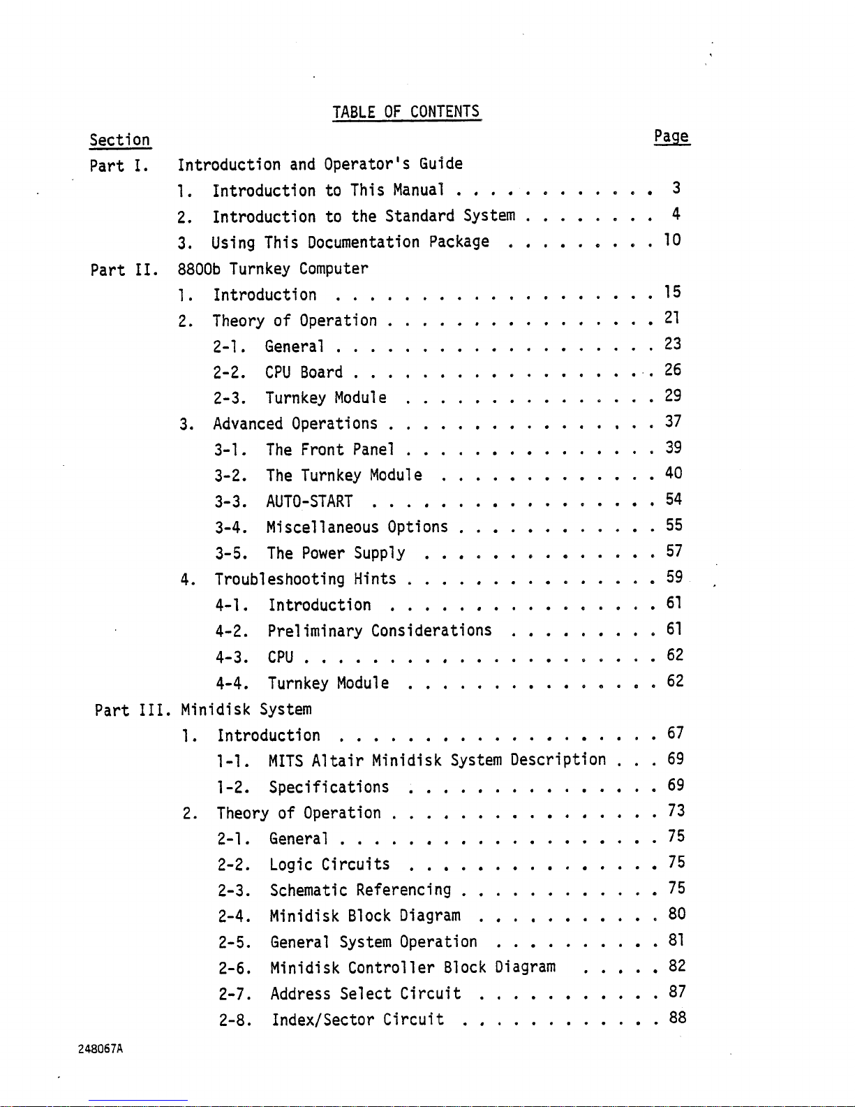
TABLE OF CONTENTS
Section £M£
Part I. Introduction and Operator's Guide
1. Introduction to This Manual . . . . 3
2. Introduction to the Standard System 4
3. Using This Documentation Package 10
Part II. 8800b Turnkey Computer
1. Introduction 15
2. Theory of Operation 21
2-1. General 23
2-2. CPU Board .26
2-3. Turnkey Module .29
3. Advanced Operations 37
3-1. The Front Panel 39
3-2. The Turnkey Module 40
3-3. AUTO-START 54
3-4. Miscellaneous Options 55
3-5. The Power Supply 57
4. Troubleshooting Hints 59
4-1. Introduction 61
4-2. Preliminary Considerations 61
4-3. CPU 62
4-4. Turnkey Module 62
Part III. Minidisk System
1. Introduction 67
1-1. MITS Altair Minidisk System Description ... 69
1-2. Specifications 69
2. Theory of Operation 73
2-1. General 75
2-2. Logic Circuits 75
2-3. Schematic Referencing 75
2-4. Minidisk Block Diagram 80
2-5. General System Operation 81
2-6. Minidisk Controller Block Diagram 82
2-7. Address Select Circuit 87
2-8. Index/Sector Circuit 88
248067A
Page 10
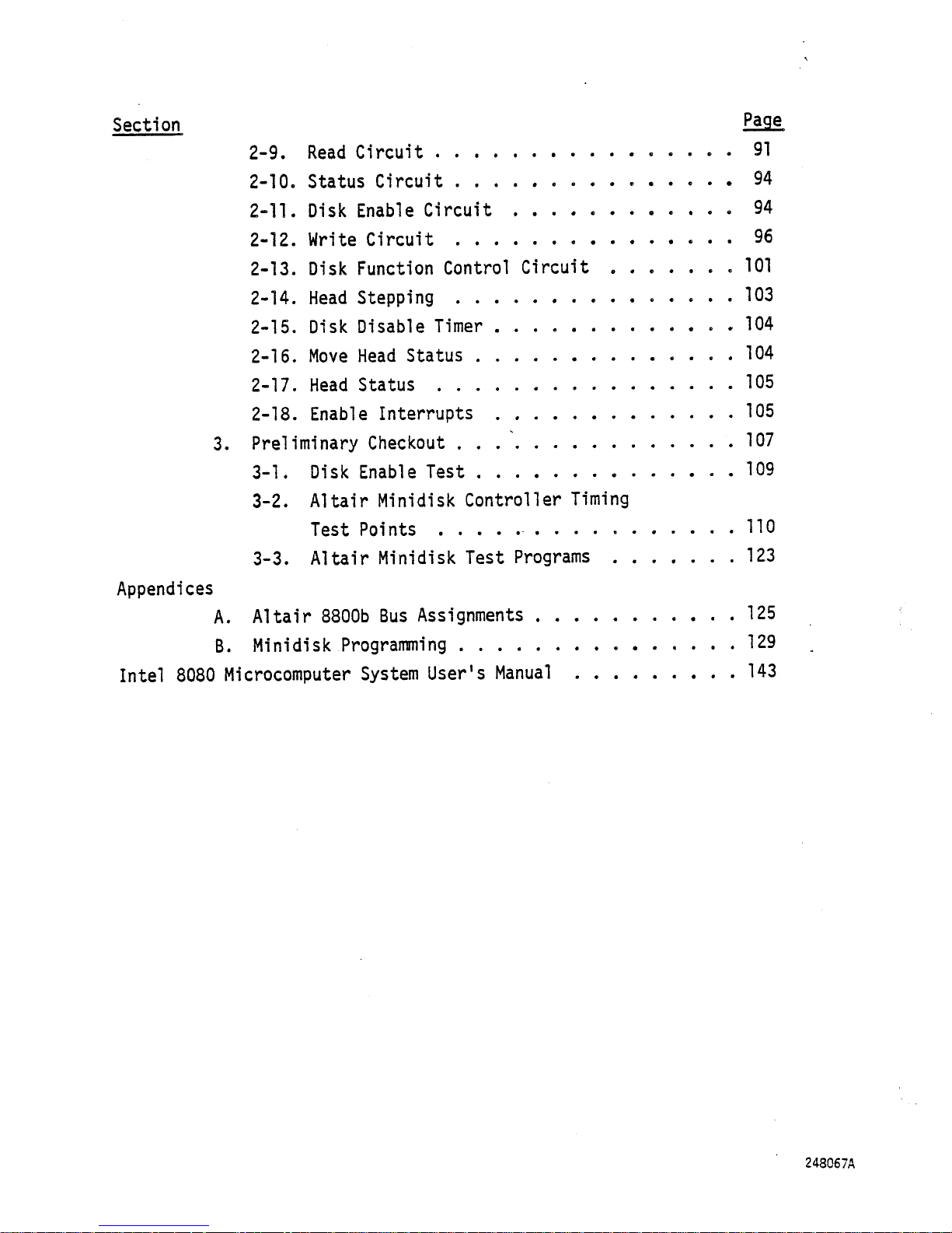
Section
Pa9e
2-9. Read Circuit 91
2-10. Status Circuit 94
2-11. Disk Enable Circuit 94
2-12. Write Circuit 96
2-13. Disk Function Control Circuit .101
2-14. Head Stepping 103
2-15. Disk Disable Timer 104
2-16. Move Head Status 104
2-17. Head Status 105
2-18. Enable Interrupts 105
3. Preliminary Checkout .107
3-1. Disk Enable Test 109
3-2. Altair Minidisk Controller Timing
Test Points 110
3-3. Altair Minidisk Test Programs 123
Appendices
A. Altair 8800b Bus Assignments 125
B. Minidisk Programming 129
Intel 8080 Microcomputer System User's Manual 143
248067A
Page 11
248067A
1/(14 Blank)
Page 12

Page 13
1. Introduction
1-1. Introduction to this Manual
The 8800b-sml and -dmare integrated computer systems that include
the Altair 8800b Turnkey microcomputer along with either one
(-sm)
or
two (dm) Altair Minidisk mass storage units.
The 8800b Turnkey computer includes the system power supply, the
Central Processing Unit (CPU) with the 8080A microprocessor and a
Turnkey Module board. The Turnkey Module is a multi-function board that
includes IK bytes of random access memory (RAM), provisions for up to
IK bytes of read only memory (PROM) (including the Minidisk Boot
Loader PROM) and a. serial input/output port (SI0) for connecting the
computer to a terminal. Part II of this documentation package documents
the 8800b Turnkey computer. Section 1 is a description of the components
of the Turnkey computer, and Section 2 is a brief summary of its theory
of operation. Section 3 is an advanced operation manual which details
procedures for expanding and modifying the standard system. Section
4 is a brief guide to troubleshooting the electronics of the computer.
The Minidisk mass storage subsystem consists of one or two Minidiskk
drives, a drive controller and an interface card for connecting the disk
system to the computer. These are all described in Part III of this
documentation package. Section 1 is a listing of the specifications of
the Minidisk subsystem. Section 2 is a summary of the theory of
operation and Section 3 is a description of procedures for initial
checkout and fault diagnosis.
The Appendices include a description of the Altair bus, instructions
for converting the power supply for use with 230 volts AC, a listing of
the Minidisk Boot Loader PROM and aids for programming the Minidisk
system in machine language.
Finally, the Intel 8080A Mtcrocomputer System User's Manual details
the structure, timing and instruction set of the 8080A microprocessor.
It also gives technical information about some of the CPU's auxiliary
circuits.
13 248067A
Page 14
1-2. Introduction to the Standard System
The standard 8800b-sm or -dm system consists of the 8800b-sm or -dm
TM -
computer and either a Teletype or Cathode Ray Tube (CRT) terminal. This
section shows how to assemble such a system from its components and how to
load and run BASIC on the assembled system.
A, Setting up the system. Carefully lift the computer unit from
its packing case and place it on a hard, flat surface. Leave enough
space on all sides so that the flow of cooling air is not impaired,
Do not connect the power cord until the terminal has been installed.
Remove the protective tabs from the Minidisk drives following
the directions printed on the tabs.
The computer is set at the factory to match the terminal shipped
with it. Therefore, to install the terminal, it is only necessary to
connect the computer and the terminal with the cable supplied with the
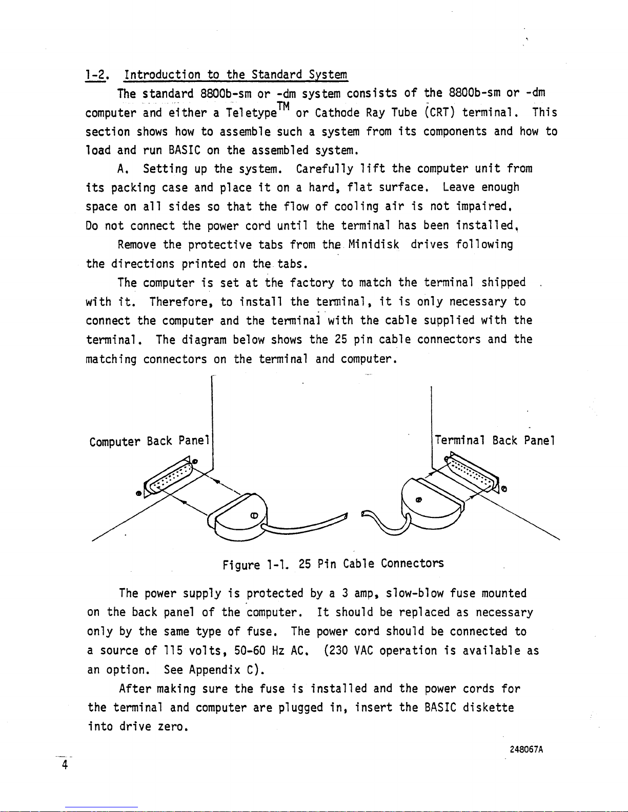
terminal. The diagram below shows the 25 pin cable connectors and the
matching connectors on the terminal and computer.
Figure 1-1. 25 Pin Cable Connectors
The power supply is protected by a 3 amp, slow-blow fuse mounted
on the back panel of the computer. It should be replaced as necessary
only by the same type of fuse. The power cord should be connected to
a source of 115 volts, 50-60 Hz AC. (230 VAC operation is available as
an option. See Appendix C).
After making sure the fuse is installed and the power cords for
the terminal and computer are plugged in, insert the BASIC diskette
into drive zero.
248067A
4
Page 15

To do this, open disk drive zero by pulling out on the door tab
(see Figure 1-2). Insert the edge of the diskette opposite the label
into the drive with the label side toward the open tab. Push the diskette
all the way into the drive and close the door tab.
Now, move the RUN/STOP switch on the front panel up to the RUN
position and turn the power switch on. The power switch has three
positions. At 12 o1clock, the unit is off and the key may be removed.
At 3 o'clock, the power is on and the front panel switches are enabled.
At 6 o'clock, the computer is on, but the front panel switches are
disabled. In this position, the key may be removed.
With the power switch on, the Power indicator should light showing
that the computer circuitry is receiving operating voltage from the
power supply. If the Power indicator does not light, turn off the power
switch and check the power cord and fuse.
Head Load Light
Diskette Slot
Door Tab
Label
Figure 1-2 Inserting the Diskette
248067A
'5
Page 16
B. Initializing BASIC. When the power is turned on, BASIC is
loaded into memory automatically. When it has been loaded, BASIC prints
MEMORY SIZE?
on the terminal to begin the initialization dialog. This question asks
the operator to specify the amount of memory to be used by BASIC programs.
Typing a number and carriage return reserves that number of bytes. Typing
just a carriage return directs BASIC to use all available read/write
memory. BASIC now prints
LINEPRINTER?
The operator types a letter and carriage return to indicate the type
of printer in use as follows:
Letter Printer
0 = LP80
C = C700
Q = Q70
If no printer is connected, any of the letters may be typed. If the
response is not 0, C or Q, however, BASIC asks LINEPRINTER? again.
BASIC now asks
HIGHEST DISK NUMBER?
In a system with 1 disk, the highest number is 0. With 2 disks, the
highest number is 1. Typing just a carriage return is equivalent to
typing 0.
Now BASIC asks the number of disk data files (random access and
sequential) to be open at one time:
HOW MANY DISK FILES?
The operator responds with the number of disk data files expected to be
open at any one time. BASIC then-prints
HOW MANY RANDOM FILES?
Here again, the operator responds with the number of random access files
expected to be open at any one time.
Now BASIC is initialized and prints the following messages:
ALTAIR MINI-DISK BASIC
REVISION 4.1 JULY 1977
COPYRIGHT 1977 BY MITS, INC.
6
248067A
Page 17
OK
BASIC is now ready for use.
At any time, BASIC may be reloaded simply by momentarily depressing
the START switch.
C. Initializing New Diskettes. Because the BASIC code takes up
so much diskette space, it is supplied on a "write protected" diskette.
This means that no programs or data may be saved on the BASIC diskette.
In addition to BASIC, the BASIC diskette includes two programs,
PIP and STARTREK, which are available to users. Before they can be run,
the BASIC diskette must be mounted (see section D below). Since the
BASIC diskette is write protected, mounting it causes a DISK I/O ERROR,
but the reading process is not affected.
The desired program may now be read from the disk and loaded into
memory. To do this, type the foil owing command:
LOAD "<program name>",<disk number>
where <program name> is the name of the desired program and <disk number>
m
is the number of the disk drive into which the BASIC disk was inserted
(usually zero).
To avoid inadvertant damage to the BASIC disk, type the following
command:
UNL0AD<disk number>
where<disk number>is the.drive number that appeared in the LOAD command
above.
Now the BASIC diskette may be removed and another diskette inserted
into the drive and mounted.
The program may be saved on the new diskette by typing the following
command:
SAVE "<program name>",<disk number>
where <disk number>is the number of the disk drive into which the new
diskette was inserted.
Subsequent to saving the program, it may be run by typing the following
comnand:
RUN "<program name^^disk rrumber>
where <disk number>is the number of the disk drive into which the diskette
bearing the program was inserted.
248067A
7
Page 18
CAUTION
Do not attempt to write programs or data onto the BASIC
diskette. This can result in FILE LINK ERRORS that can make
the BASIC diskette unusable. Before writing anything on disk,
unload and remove the BASIC diskette.
If the diskette has never been used it must be initialized before
it can be used. This is done by typing the following command:
DSKINI <disk number>
where disk number is the number of the disk drive on which the blank
diskette is loaded. The DSKINI command marks all the sectors on the
diskette as being empty. BASIC reads these marks to determine sector
boundari es.
CAUTION
Only new, blank diskettes need to be initialized.
Using DSKINI on a diskette that contains files destroys
all the files. DISKINI should, therefore, be used with
extreme caution. The DSKINI process takes about 2 minutes
per diskette. When it is finished, BASIC prints OK.
D. Mounting Diskettes. To ready a diskette for reading or writing,
type the
foil
owing command:
MOUNT <disk number>
Omitting the disk number causes all disks in the system to be mounted.
After a few seconds, BASIC prints
OK
to indicate that the disk is ready for use.
Before removing a mounted disk from a drive, type the following
command
UNLOAD <disk number>
Omitting the disk number unloads all mounted disks.
8
248067A
Page 19
E, Diskette Specifications and Care. The 8800T sm and dm use
5 1/411, hard-sectored diskettes. Diskettes are available from MITS (Part
number 102501) or may be purchased from any Altair Computer Center.
The notch on the side of the diskette engages a switch in the
drive which enables the write circuitry. Covering the notch with a
piece of tape makes writing on the diskette impossible. The BASIC
diskette is protected in this manner.
CAUTION
Unprotecting the BASIC diskette can cause destruction
of the BASIC interpreter. DO NOT remove the BASIC
diskette protection tab.
Several handling precautions will maximize the life and usefulness
of diskettes and drives.
\
1. Return diskettes to their storage envelopes when they are not
in use. Do not leave them in the drive.
2. Keep diskettes away from magnetic fields. Fields may be
caused by fluorescent lights, transformers or large pieces
of magnetizable materials.
3. Mark the diskette label only with felt tip pen. Do not use
ball point pen or pencil.
4. Keep dust, and other particulate matter away from diskettes.
5. Keep diskettes away from excessive sunlight and heat.
6. Never touch the diskette surface (through the head access
window) or attempt to clean it.
F. Miscellaneous Information. Since the address of the Mini-Disk
controller is the same as the standard size floppy disk controller
(88-DCDD) the standard size disk drives may not be used in the 8800T-sm
or-dm system.
A timing circuit in the Mini Disk Controller turns off the drive
motor 6.4 seconds after the last access operation to minimize drive
wear.
248C67A
9
Page 20
1-3, Using this Documentation Package
The remainder of the documentation in this package contains reference
material for operating and maintaining the components of the system.
Three commonly encountered situations which require the use of
this reference material are 1) expansion of the system memory, 2) adding
or modifying input/output peripheral equipment and 3) adding special
purpose PROM functions. The procedures for making these modifications
are sketched below along with references to more detailed information.
The references are either to the manuals or to the page numbers in this
documentation package in which the information may be found.
NOTE
Before working on the inside of the computer case make
sure the power is off and the power cord disconnected from the
line.
To remove the case cover, remove the two bolts in the upper
corners of the back panel. Then slide the cover back and lift
it off.
To remove a card, pull straight up on both ends of the
card. Carefully remove any cable connectors when the board is
free.
To insert a card, connect the necessary cables and position
the board so the edge connector is down and the component side
of the board is to the right as viewed from the front of the
unit. Insert the card into the card guides and slide it
straight down until it makes contact with the connector at the
bottom of the slot. Apply firm, steady pressure to the upper
edge of the card until the board seats in the connector. The
top edge should be flush with the top of the card guides.
A. Expanding Memory. System memory expansion is accomplished by
adding memory boards or replacing them with boards of higher capacity.
Use the following procedure to make these changes:
248C67A 20
Page 21
1) Set the addresses of the new boards (memory board manual).
2) Insert the boards in the chassis
(p.
10 ).
3) Change the address of the RAM block on the Turnkey Module
board, if necessary to avoid conflicts with the new memory
addresses (p. 40 ).
B. Modification of Input/Output Arrangements. Input and output
arrangements can be changed either by adding new peripheral devices
(terminals, mass storage, printers, etc.) along with their associated
interface boards or by changing the device connected to the Turnkey
Module SIO port.
1) If a new interface board is being installed, set the port
address, data transfer rate (or baud rate) and signal type
(interface board manual).
2)Install all necessary cables and insert the board in the chassis
(interface board manual and p. 10).
3) If the SIO port is to be connected to a different device or
otherwise changed, set the desired address, data transfer rate
and
s ignal
type (p. 42ff).
4) If the new device is to be the console terminal for BASIC
or DOS, set the sense switch on the Turnkey module board to
conform to the device (p. 41 and BASIC or DOS manual).
C. Adding Special PROM Functions. The Turnkey Module has sockets
for up to four 256 byte PROM chips. These PROMs can be used to store
any programs or data that must be permanently retained. Several
pre-programmed PROMs are available for the 8800 series microcomputers
including a Turnkey PROM Monitor and a multi-purpose bootstrap loader
for loading programs from paper tape and cassette. In addition, userwritten programs can be retained in PROM for use in dedicated applications.
To install these PROM functions, use the following procedure:
1) Set the address of the Turnkey Module PROM block to the first
location of the IK byte block that includes the address of
the new PROM (p. 40, PROM documentation).
248067A
11
Page 22
2) Insert the new PROM in the proper socket on the Turnkey Module
board. The first address of the first PROM socket is the address
set in step 1. The first address of the second socket is the
Board address plus 256 and so on (p.40).
3) Set the starting address of the new program in the AUTO-START
switches, if the program is to be executed automatically when the
power is turned on or when the START switch is actuated. Note
that the Turnkey Module is supplied with the Mini Disk Boot Loader
PROM at the AUTO-START address to automatically load BASIC or DOS.
Changing the PROM or AUTO-START addresses will disable this feature
(p. 54).
NOTE
A Turnkey PROM Monitor is a good investment for an expanded system. The Monitor allows examination and modification of any memory location from the terminal. It lets
the operator dump the contents of any range of memory locations and transfer control of the computer's execution to
any address. Putting the Monitor at the AUTO-START address
allows the Monitor to be entered at any time, simply by
actuating the START switch. This provides a useful reset
function for BASIC programs. If a programs hangs in an
infinite loop or an impossible I/O function, reentering the
Monitor with the START switch and jumping to location zero
causes BASIC to print OK and await further instructions.
22 248067A
Page 23

IM111I
n
mmm
!
MIT
DD
hh
248067A
13/(14 Blank)
Page 24

Page 25

P(1TP
gm
fW
Up LI
I
N
1
ca
tfl
248067A
15/(14 Blank)
Page 26

Page 27
1. INTRODUCTION
The Altair 8800b Turnkey computer is housed in a standard Altair sys-
tem case and contains the following elements:
-Power supply and motherboard assembly
-CPU board with the 8080A microprocessor
-Turnkey Module with memory and I/O circuitry
-Front panel board
The heart of the computer is the Central Processing Unit (CPU) board
(Figure 1-2) which holds the 8080A microprocessor and its associated circuitry. The 8080A performs all the logical and arithmetic computations
for the system. It also supplies control and status signals for the other
system components. Other circuitry on the CPU board provides clock signals
and synchronization functions.
The Turnkey module (Figure 1-3) is a general support board for the
Turnkey system which includes memory, I/O and AUTO-START control. The memory
section has IK bytes of random access memory (RAM) and positions for up to
IK bytes of read-only memory (ROM). Random access memory stores information
that can be read, written or changed at will. RAM is volatile, however,
and information is lost when power is interrupted. Programmable Read-only
memory (PROM) is non-volatile. Information in PROM is always present whether
the power is on or not. Thus, PROM can store programs and data which must
be permanently retained. The computer cannot write information into PROM,
however. A special PROM programmer must be used to do this, although factoryprogrammed PROMs are available for some widely used functions.
The serial Input/Output channel (SIO) connects the parallel data bus
in the computer to serial input/output devices, such as Teletypes, CRT terminals,
modems, etc. The SIO may be configured to accommodate a variety of terminal
types and speeds to match virtually any serial I/O arrangement.
The AUTO-START feature is the key to the Altair 8800b Turnkey computer's
ease of operation. When the computer's power is turned on or the START switch
is actuated, the AUTO-START logic forces the computer to execute the instruction at a pre-selected address in PROM. The address could be the beginning
of a series of instructions to load a program from an I/O device, the start
of a monitor program or a dedicated application program.
24S067A 17
Page 28

Front Panel switches (Figure 1-4) include the power switch, which
provides system security as well as turning the power on or off, and
switches that start and stop execution of programs. Indicators on the
Front Panel monitor the computer system's operation.
Power, data, addresses, status and control signals and miscellaneous
pulses are carried by the system bus on the motherboard. The bus is
fully parallel, meaning that all signals are available to all boards
plugged into the motherboard's sockets. This allows for easy and
quick system expansion. The motherboard can accommodate the CPU and
Turnkey Module boards plus up to 16 additional boards.
The Power Supply provides all the power voltages required by the
Altair 8800b Turnkey system components. The supply has enough capacity
to allow expansion of the sytem by addition of as many I/O and memory
boards as will fit in the system case.
18
248067A
Page 29
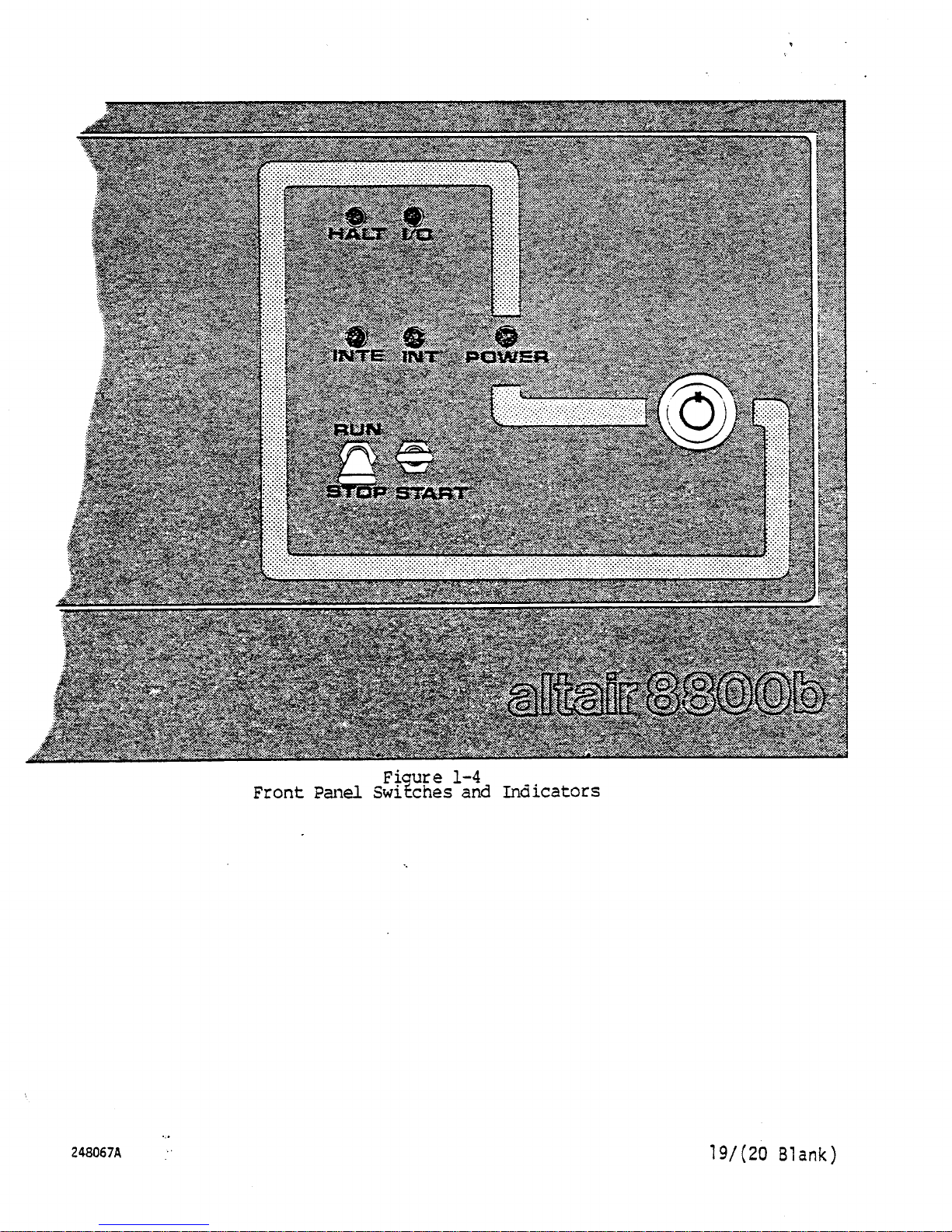
Front Panel Switches and Indicators
Figure 1-4
248067A
19/(14 Blank)
Page 30

Page 31

urn
rin
i
'fnW?[
iUdui
!W 0?»
seal
^rnnrfi
248067A
21/(14 Blank)
Page 32

Page 33
L. theory of operation
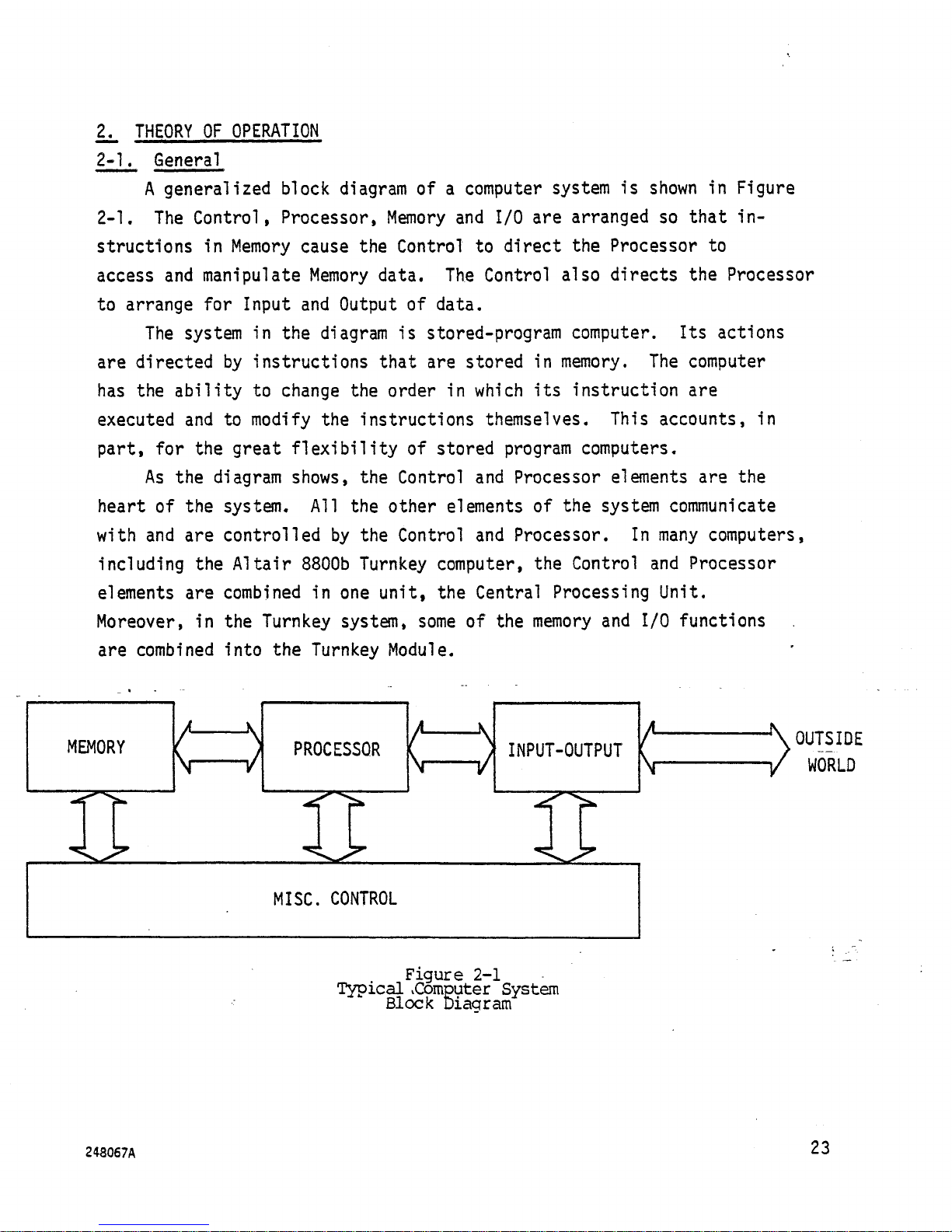
2-1. General
A generalized block diagram of a computer system is shown in Figure
2-1• The Control, Processor, Memory and I/O are arranged so that instructions in Memory cause the Control to direct the Processor to
access and manipulate Memory data. The Control also directs the Processor
to arrange for Input and Output of data.
The system in the diagram is stored-program computer. Its actions
are directed by instructions that are stored in memory. The computer
has the ability to change the order in which its instruction are
executed and to modify the instructions themselves. This accounts, in
part, for the great flexibility of stored program computers.
As the diagram shows, the Control and Processor elements are the
heart of the system. All the other elements of the system communicate
with and are controlled by the Control and Processor. In many computers,
including the Altair 8800b Turnkey computer, the Control and Processor
elements are combined in one unit, the Central Processing Unit.
Moreover, in the Turnkey system, some of the memory and I/O functions
are combined into the Turnkey Module.
Figure 2-1
Typical vComputer System
Block Diaqram
248067A
23
Page 34
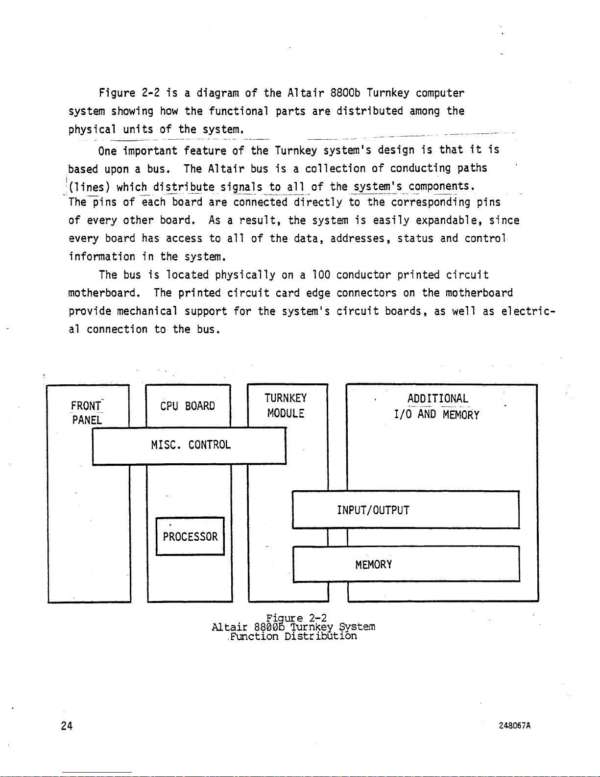
Figure 2-2 is a diagram of the Altair 8800b Turnkey computer
system showing how the functional parts are distributed among the
physical units of the system. _
One important feature of the Turnkey system's design is that it is
based upon a bus. The Altair bus is a collection of conducting paths
(lines) which diTribute signals to all of the system's components.
The~pins of each board are connected directly to the corresponding pins
of every other board. As a result, the system is easily expandable, since
every board has access to all of the data, addresses, status and control
information in the system.
The bus is located physically on a 100 conductor printed circuit
motherboard. The printed circuit card edge connectors on the motherboard
provide mechanical support for the system's circuit boards, as well as electric-
al connection to the bus.
Figure 2-2
Altair 88005 Turnkey System
Function Distribution
24
248067A
Page 35
The bus has 16 Address lines, 8 Data-in lines carrying data to the
CPU, 8 Data-Out lines carrying data from the CPU and lines carrying
pulses that indicate the status of the system and serve various control
functions, A list of the conductors on the Altair system bus is in the
Appendix.
The activity on the bus corresponds to six machine cycles; Memory
Read and Write, I/O In and Out, Interrupt and Halt. The functions of
the various bus lines depend on what cycle is currently in progress.
In a Memory cycle, the address of the memory location to be read
or written is carried on the address bus. The Data-in bus carries
data or instruction codes from memory to the CPU during a Memory Read.
The Data-Out bus carries data from the CPU during a Memory Write. In an
I/O cycle, the Address bus carries the address of the I/O port through
which the data transfer is to take place. The port address is only
eight bits long, so it is carried both in the high and low order bytes of
the 16 bit Address bus. The Data-in bus carries information from
the port to the CPU during an Input cycle. Similarly, the Data out buscarries information from the CPU to the port in an Output cycle.
The Interrupt cycle is provided so that peripheral devices can
gain access to the bus. In the absence of interrupts, the CPU can
be programmed to check its peripheral devices periodically and service
them as they have information to transfer. An input device, for example,
waits until the CPU signals that it is ready for input. This arrangement
is simple, but it is often inefficient, since the CPU is required to
poll the I/O devices whether or not there is information to be transferred.
248067A
25
Page 36
In an interrupt driven system, on the other hand, the I/O device
signals the CPU when it is ready to transfer data. This signal is called
an Interrupt Request. If the CPU Interrupt Enable bit is set to 1,
the CPU acknowledges the Interrupt Request. Otherwise, the request is
ignored. In an Interrupt cycle, the CPU fetches an instruction which
causes the computer to interrupt the execution of its current program
and begin executing another program (called an interrupt service routine)
at a special location in memory. The computer also stores the location
of its current instruction so that it can return to the place where it
left off when the interrupt service routine is completed. The interrupt
scheme allows the computer to work on a program until a peripheral device
has information to transfer. The CPU can then accept the information and
take the necessary action without losing track of the program in progress.
A special machine cycle is provided for direct memory access.
During the Hold state, the CPU is effectively disconnected from the bus.
This allows a direct memory access device, if it is used, to take control
of the bus and transfer information directly to and from memory. For more
information on machine cycles, see the Intel 8080 machine cycles,
see the Intel 8080 Microcomputer System User's Manual (abbreviated IMSUM),
section 2, pp 3-11.
2-2. The CPU Board
NOTE
In the following descriptions, the names of signals appear
in capital letters. Signal names which are barred (PRESET,
for example) are active LOW. That is, they are LOW (0 volts)
when activated and HIGH (+5 volts) otherwise. All other signals
are active HIGH.
The address and data lines represent binary 1 as HIGH
and binary 0 as LOW.
On the Turnkey module, the sense switches and the address
switches for RAM, PROM and AUTO-START allow manual entry of data
and addresses. The two states of each switch -on and off- correspond to the two states of a binary digit - 1 and 0. The bits
represented by the sets of switches can, therefore, be treated by
the computer in the same way as any other data or address bits.
Moving a switch in the direction of the arrow next to each set of
switches puts the switch in the 1 position.
) 248067A
Page 37
0:
+ 8V
(UNREG)
L3
J- 08 J^C6
-p
.IUF J 3SUF
R22
VRI
7805
Li
3
-X
CI
35UF
. sc
IUF
-VCC
H~6VRE<2)
+ 18 V
L4
lc»o
ir
-y.tuF
j
C9
35UF
VR2
7812
L2
[2 r^L.
J-
C3
I
I
35UF "T--IWF
4—dL
-V0DH-I2V
REG)
8C
IUF
50,
100
6RD
L6
*>VBB (-5V
REG)
REF
DESiG
TYPE
VCC GRO
OTHER
REF
DESIG
TYPE
VCC
GRD
OTHER
M
8080A
20
2
G
,B
74LS04
14 7
J.X.R.V.
N.U.P
74368
OR
8T98
16
8
C
74LSI3
OR
74LS20
14 7
J.X.R.V.
N.U.P
74368
OR
8T98
16
8
C
74LSI3
OR
74LS20
14 7
K 8212
24
12
S,
Y
74LSI4
14
7
D,E
8216 16 8
F
8224
16
8
VDD-9
P.W
74367
16
8
A
4009
1 8
VDO «16
Figure
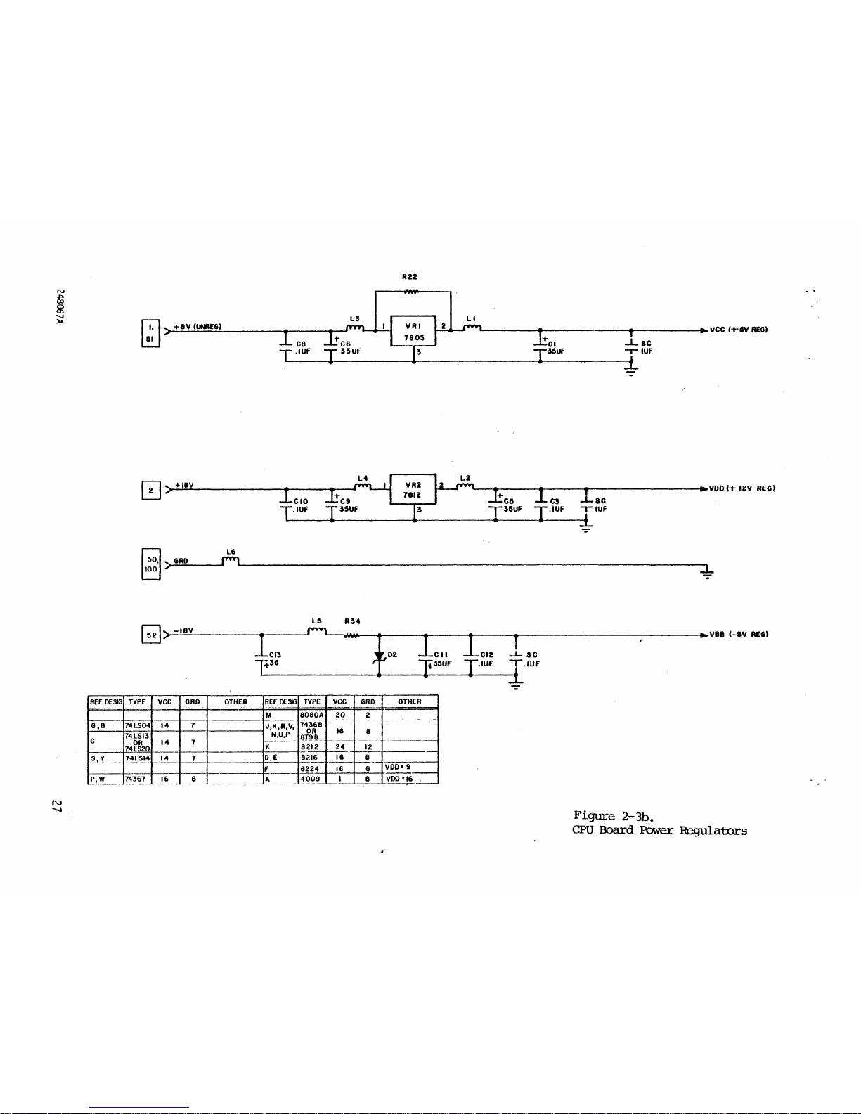
2~3b.
CPU
Board Power Regulators
Page 38
The CPU board contains the 8080A microprocessor, its timing and auxiliary control
circuits. It also contains buffers and line drivers for the system bus. The
heart of the CPU (and the whole computer system) is the 8080A microprocessor.
All of the other circuitry on the board serves to support the microprocessor
and connect it to the rest of the system.
r
____
A. The Microprocessor. The 8080A is IC M on the schematic, Figure
2-3a. For a complete description of the internal organization and timingid
of the 8080A, see the IMSUM, Chapter 2.
B. Clock and Synchronization. The 8224 clock generator (IC F on the
schematic) provides the two-phase, 2 MHz clock for the 8080A at the required
0 and 12 volt levels. The master timing reference for the 8224 is an ex-
ternal 18 MHz crystal. The system timing frequency can be changed by replacing the crystal.
The clock generator also synchronizes the 8080A's READY and RESET inputs
and provides a status strobe signal (STSTB) that is used to load the 8212
status latch. The READY signal is the logical product (AND) of bus signals
XRDY, PRDY, XRDY2 and FRDY. Normally, only PRDY is used for memory synchronization; the others are set to logical 1 by pullup resistors. The bus signal
PRESET is filtered, lengthened, shaped and synchronized by the 8224 to generate
the RESET input for the 8080A. The STSTB signal is generated as soon as the
status information is available on the 8080A data lines.
C. The Status Latch. At the beginning of each bus cycle, status information is presented momentarily on the 8080A data lines. This information is stored in the 8212 latch so that the data lines may be used for other
information later. The 8212 is IC K on the schematic. For a complete description of the status information and its timing, see page 2-6 of IMSUM.
The 8212 is described on page 5-101 of the same manual.
D. Buffers.
1) Bus splitters. Information is communicated to and from the 8080A
through an eight-bit, bidirectional data bus. This bus is buffered by two
8216 bidirectional bus drivers to form a TTL compatible, bidirectional bus
on the CPU board. The direction of the 8216,s is controlled by PDBIN.
28
248067A
Page 39
At the other end of the CPU bus are tri-state buffers that split the
bidirectional data bus into Data-in and Data-Out busses which are brought
out to the system bus. The buffers shown in zones B-3 and B-4 transfer data
from the system Data-in bus to the bidirectional bus when both PDBIN and
DIG! are HIGH. (DIG! is normally HIGH unless the bidirectional bus is being
accessed through connector P3. When either PDBIN or DIG! are LOW, the buffers
are put in a high impedance state and no information is transferred through
them. Similarly, the buffers in zones C-2 and C-3 transfer data from the
CPU bus to the Data-Out system bus when the signal DO DSBL is HIGH.
If no information is present on the Data-in bus, all eight lines are
pulled HIGH by resistors on the CPU board. When a interrupt is acknowledged,
this forces a RST 7 instruction onto the bus if the Vector Interrupt Board
is not used.
2) Input buffers. All input lines to the CPU board are buffered by
TTL circuitry. Unused lines are pulled HIGH by resistors which also allow
any one of several boards to pull any input line LOW. A line is normally pulled
LOW either by an open collector driver or a tri-state driver, with the condition
that no more than one tri-state driver may be enabled at one time.
Examples of these input lines are PINT and PHOLD in zone D-8, the
READY lines (PRDY, etc.) in zone A-7, PRESET in zone A-6, and the driver
disable lines throughout the schematic.
3) Output buffers. All outputs from the CPU board are buffered to drive
30 standard TTL loads. The lines are collected into four groups, Address lines,
Data Out lines, Status lines and a Control group made up of PWR, PDBIN, PWAIT,
PSYNC, PHLDA and PINTE. Each group of lines may be disabled as a group by
signals from the bus.
2-3. The Turnkey Module
The Turnkey Module contains 1024 bytes each of RAM and PROM, a serial
I/O channel, AUTO-START logic, sense switch, the front panel board and logic
and miscellaneous logic. The Turnkey Module schematic is shown in Figures 2-4
a, b and c.
A. RAM and PROM. The RAM and PROM memories and their control logic are
shown in the schematic diagrams, Figures 2-4 a and c.
248067A
29
Page 40
1) The incoming PROM address is compared with the starting PROM address
by the NAND gate IC D. If the incoming address is in the IK block selected for
PROM, the output of IC D, active LOW, enables the PROM address decoder,
IC Za, which selects one of the PROM ICs. Up to four PROM chips may be
installed. The output of IC D is also combined with the output of the
I/O address detector in a NOR gate, the output of which causes the CPU
to execute a WAIT state and enables the data bus interface, IC's P and R.
The selected PROM drives the bidirectional data bus and the interfaces
P and R put the selected data on the Data-in system bus.
2) An address of a byte in RAM is detected by IC B. The output
of IC B is active if a start sequence is not in progress and the current
machine cycle is not an I/O cycle or an interrupt. Therefore, the only
time a RAM address is detected is when the machine cycle is a memory
cycle or a Halt cycle. The output of IC B enables the RAM ICs and the
data bus interfaces P and R. The direction of the data bus is controlled,
by the MWRT pulse described in paragraph 2-3F. When RAM is
selected, data at the address is put on the bidirectional bus. If
the cycle is a memory read, the cycle is complete. If it is a write
cycle, the direction of the data bus interfaces is momentarily reversed,
overdriving the RAM output drivers. Pulsing the RAM write inputs then
causes the data on the bus to be written in the addressed location.
30
248067A
Page 41
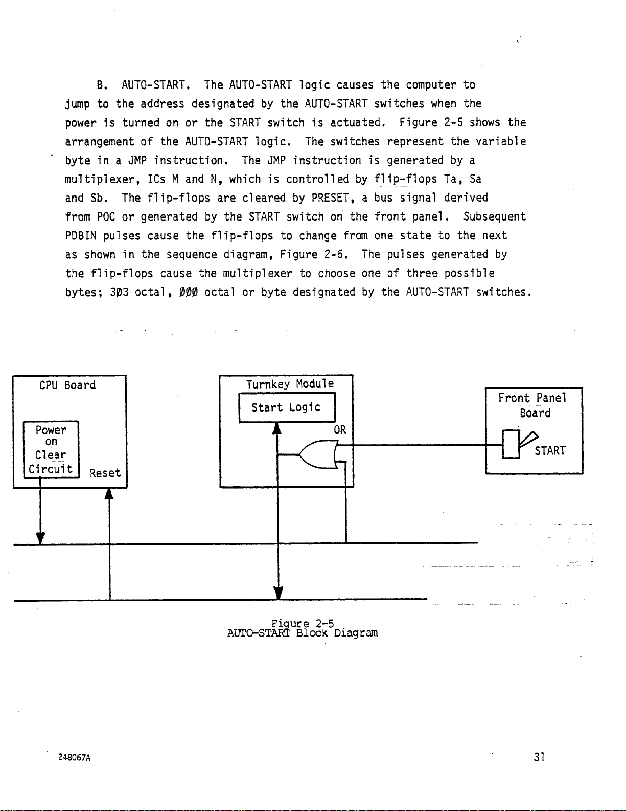
B. AUTO-START. The AUTO-START logic causes the computer to
jump to the address designated by the AUTO-START switches when the
power is turned on or the START switch is actuated. Figure 2-5 shows the
arrangement of the AUTO-START logic. The switches represent the variable
byte in a JMP instruction. The JMP instruction is generated by a
multiplexer, ICs M and N, which is controlled by flip-flops Ta, Sa
and Sb. The flip-flops are cleared by PRESET, a bus signal derived
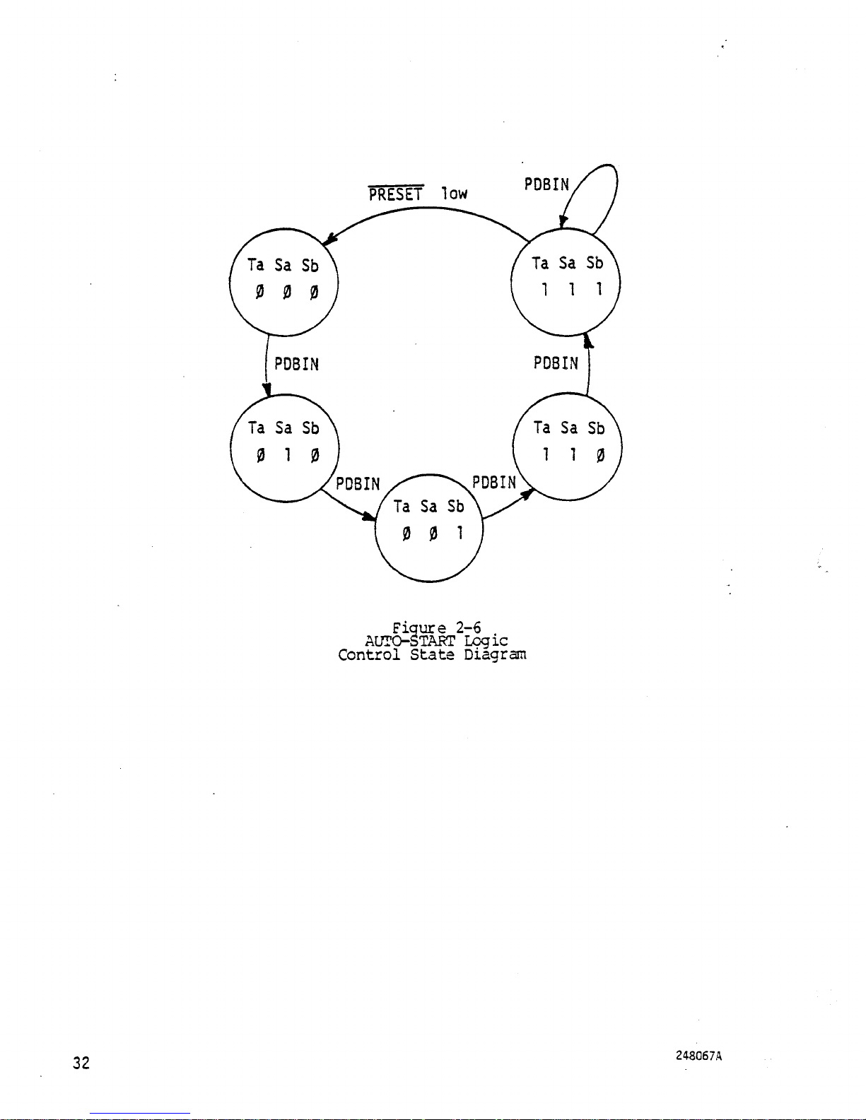
from POC or generated by the START switch on the front panel. Subsequent
PDBIN pulses cause the flip-flops to change from one state to the next
as shown in the sequence diagram, Figure 2-6. The pulses generated by
the flip-flops cause the multiplexer to choose one of three possible
bytes; 303 octal, 000 octal or byte designated by the AUTO-START switches.
Figure 2-5
AUTOSTART Block Diagram
248067A
31
Page 42
PRESET
low
PDBIN
Ta Sa Sb
0
0 0
PDBIN
Ta Sa Sb
0 1 0
PDBIN
Ta Sa Sb
0 0 1
Figure
PDBIN
2-6
AUTO-START Logic
Control State Diagram
Ta Sa Sb
1 1 1
PDBIN
Ta Sa Sb
1 1 0
32
248067A
Page 43
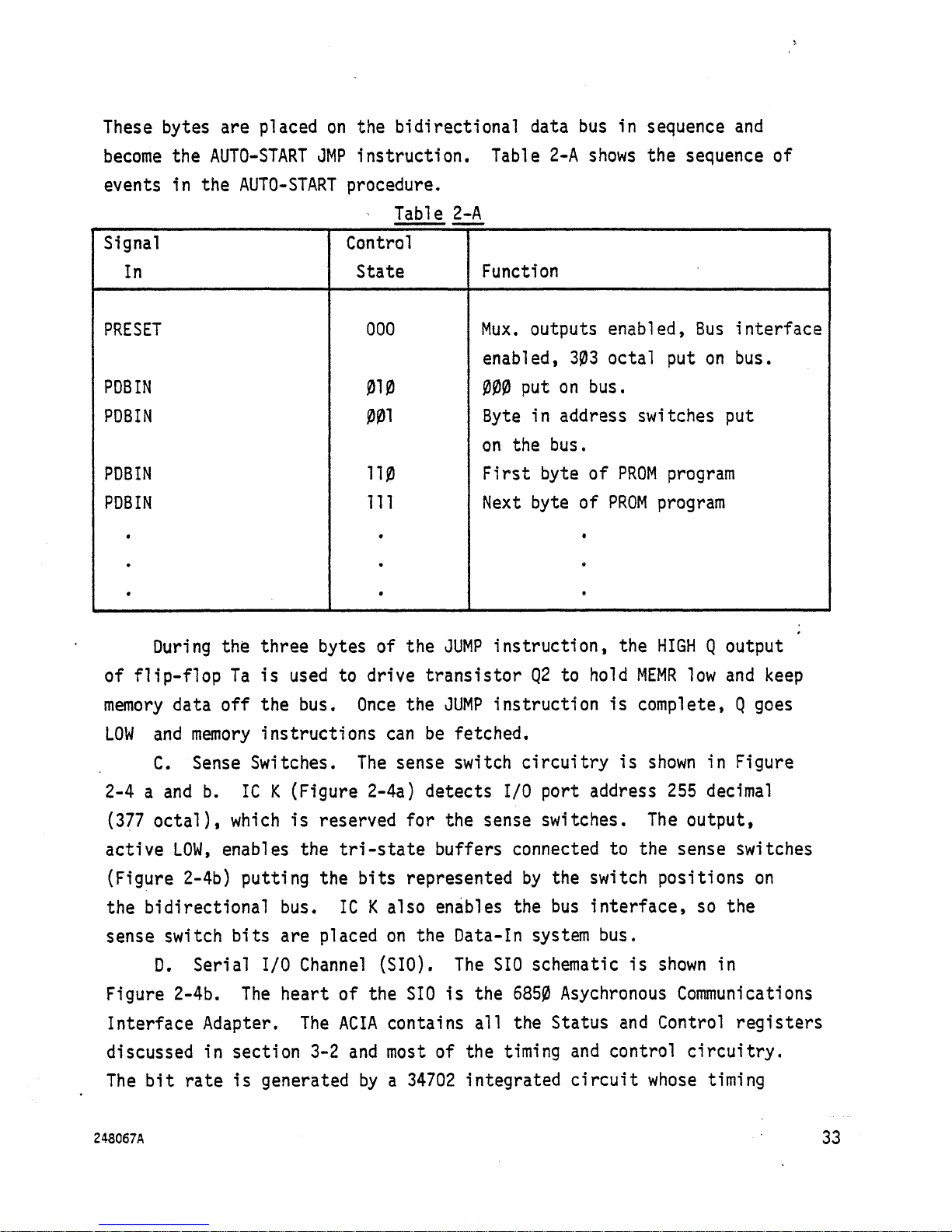
These bytes are placed on the bidirectional data bus in sequence and
become the AUTO-START JMP instruction. Table 2-A shows the sequence of
events in the AUTO-START procedure.
Table 2-A
Signal
Control
In
State
Function
PRESET
000 Mux. outputs enabled, Bus interface
enabled, 303 octal put on bus.
PDBIN
010
000 put on bus.
PDBIN
001
Byte in address switches put
on the bus.
PDBIN
110
First byte of PROM program
PDBIN
•
*
111
Next byte of PROM program
«
0
e
During thfe three bytes of the JUMP instruction, the HIGH Q output
of flip-flop Ta is used to drive transistor Q2 to hold MEMR low and keep
memory data off the bus. Once the JUMP instruction is complete, Q goes
LOW and memory instructions can be fetched.
C. Sense Switches. The sense switch circuitry is shown in Figure
2-4 a and b. IC K (Figure 2-4a) detects I/O port address 255 decimal
(377 octal), which is reserved for the sense switches. The output,
active LOW, enables the tri-state buffers connected to the sense switches
(Figure 2-4b) putting the bits represented by the switch positions on
the bidirectional bus. IC K also enables the bus interface, so the
sense switch bits are placed on the Data-in system bus.
D. Serial I/O Channel (SIO). The SIO schematic is shown in
Figure 2-4b. The heart of the SIO is the 6850 Asychronous Communications
Interface Adapter. The ACIA contains all the Status and Control registers
discussed in section 3-2 and most of the timing and control circuitry.
The bit rate is generated by a 34702 integrated circuit whose timing
248067A
33
Page 44
reference is a 2,4576 MHz crystal. Jumpers are provided to set the.
output rate of the 34702 at 1, 16 or 64 times the required bit rate.
Input signals are received by RS232 receivers that may be made
compatible with TTL or current loop signals by means of jumper-selected
pull up resistors. TTL or RS232 outputs may be selected by jumpers or
by internal cable wiring.
E. Front Panel. The front panel logic is contained on the Turnkey
Module board. The indicators and switches are connected to the
Turnkey Module by a cable and MoT ex connectors. The schematic diagram
for the front panel circuitry is in Figure 2-4a.
The bus signals PHLTA, PINTE and PINT are buffered to drive the
indicators HALT, INTE and INT, respectively. The I/O indicator is
driven by the logical sum (OR) of the INP and OUT signals. The POWER
indicator monitors the +5 volt supply on the Turnkey Module.
The bus signal PRDY is grounded when the RUN/STOP switch is in the
STOP position. PRESET is grounded momentarily by the START switch
which, in turn, initiates the AUTO-START sequence. Contact bounce
is filtered out on the CPU board to generate a reset signal suitable
for the CPU.
F. Miscellaneous Signals. Several miscellaneous signals are
handled by the rest of the circuitry on the Turnkey Module. Some are
optional and may be selected by jumpers.
1. MWRT is generated if the jumper from Ml to M2 is installed. In the
full front panel version, MWRT is generated by the front panel
logic and is used by memory boards of write functions.
2. PROT and UNPROT are used on the standard model of the Altair 8800b
for memory protect and unprotect functions. As supplied, the
Turnkey Module grounds PROT and pulses UNPROT with phase 2 of the
clock to unprotect all memory as it is accessed. This feature
may be disabled by removing the jumpers from 2 to UM and from G to
PM.
34
248067A
Page 45
3. AUX CLR is normally pulled HIGH by a resistor on the Turnkey Modlue,
but insertion of optional jumpers as described in section 3-4b
allows the signal to be used.
G. Power. All power used on the Turnkey Module and Front Panel
boards comes from the +18 volt, -18 volt and +8 volt lines on the
motherboard. The Turnkey Module^ power regulator circuitry is shown
in Figure 2-4a. The +5 volt supply is derived from the +8 volt line by
an IC regulator. The +9 volt supply comes from the +18 volt line
through a zener regulator and the -0 volt supply is derived by a
transistor-zener regulator from the -18 volt line.
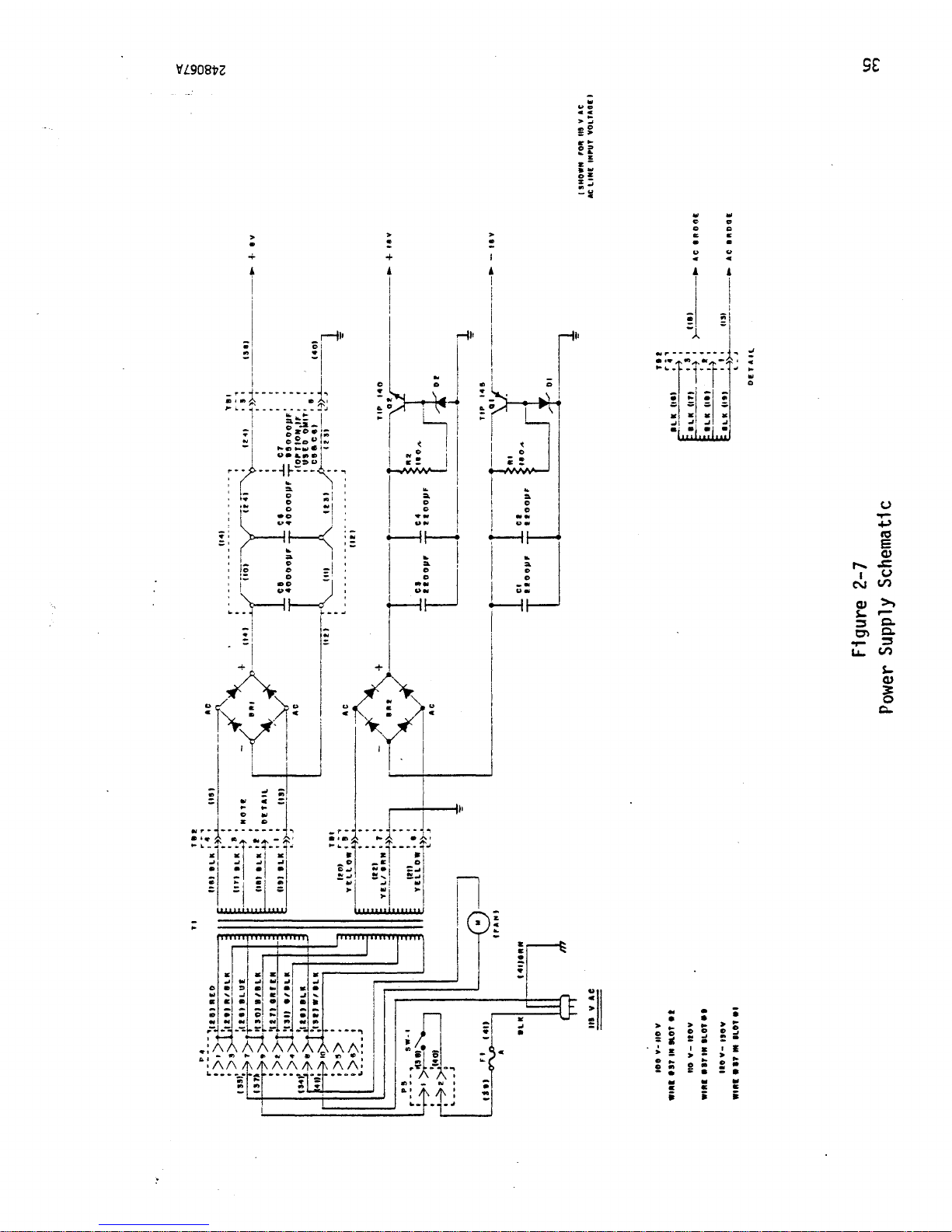
Figure 2-7 is the schematic for the power circuits in the 8800b case.
The +18 and -18 volt supplies are pre-regulated. The +8 volt supply is
not regulated, but it is adjusted by the taps on the secondary of the
power transformer.
248067A
35
Page 46
V£908t?2
> mi
© 5
10
E
CD
r^ -c
i u
C\J to
0)
= I
=
Lu
s-
<D
S
CL.
sin?*
i £ i 5 i ;
St s ; S •
Page 47

248067A
37/(38 Blank)
Page 48

Page 49
3. ADVANCED OPERATION
3-1. This Front Panel
The Front Panel contains the functional switches and status indicators
for controlling and monitoring the computer. A list of the switches and
indicators along with their functions follows:
Power switch
POWER indicator
RUN/STOP switch
START switch
HALT indicator
I/O indicator
INT indicator
INTE indicator
Turns power on and off. Key-lock switch
Indicates that power is on. Monitors the +5
volt supply on the Turnkey Module.
Causes the computer to run the program in memory
when placed in the RUN position. Execution stops
in the middle of the next machine cycle after
the switch is moved to the STOP position. Moving
the switch back to RUN continues execution at the
point where it was stopped.
When actuated, stops execution. When released,
starts execution at the START address selected
by switches on the Turnkey Module. If the
switch is actuated when the RUN/STOP switch is in the
STOP position, the computer stops in the middle
of the START sequence. Moving RUN/STOP to RUN
continues the START sequence.
Indicates that the computer is stopped either
because a HALT instruction has been executed or
because the PRESET line is LOW.
Indicates data transfer to or from an I/O port.
Indicates that an interrupt is being requested.
Indicates that the Interrupt Enable bit is set
in the CPU and that the computer may be
interrupted. When the INTE indicator is off,
interrupt requests have no effect.
248067A
39
Page 50
3-2. The Turnkey Module
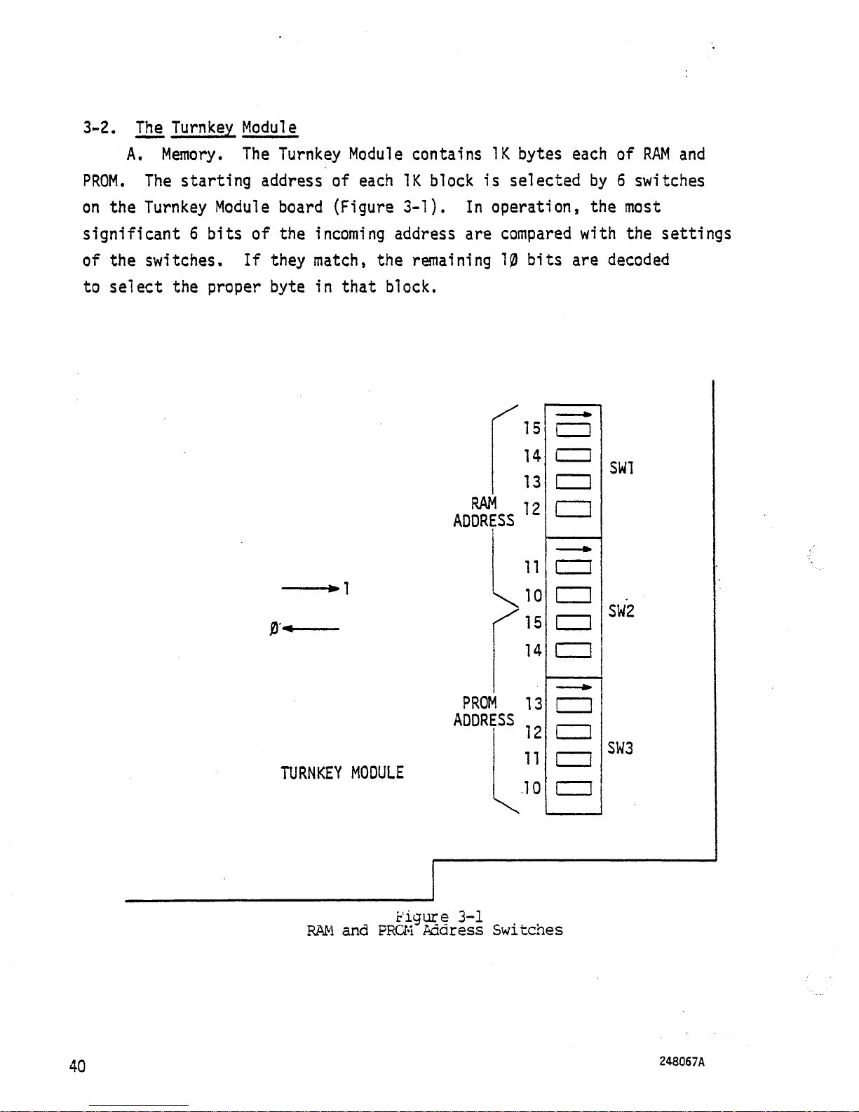
A. Memory. The Turnkey Module contains IK bytes each of RAM and
PROM. The starting address of each IK block is selected by 6 switches
on the Turnkey Module board (Figure 3-1). In operation, the most
significant 6 bits of the incoming address are compared with the settings
of the switches. If they match, the remaining 10 bits are decoded
to select the proper byte in that block.
RAM
ADDRESS
TURNKEY MODULE
15
14
13
12
11
10
15
14
PROM 13
ADDRESS
11
.10
SWl
SW2
SW3
figure 3-1
RAM and FRCM Address Switches
4Q 248067A
Page 51
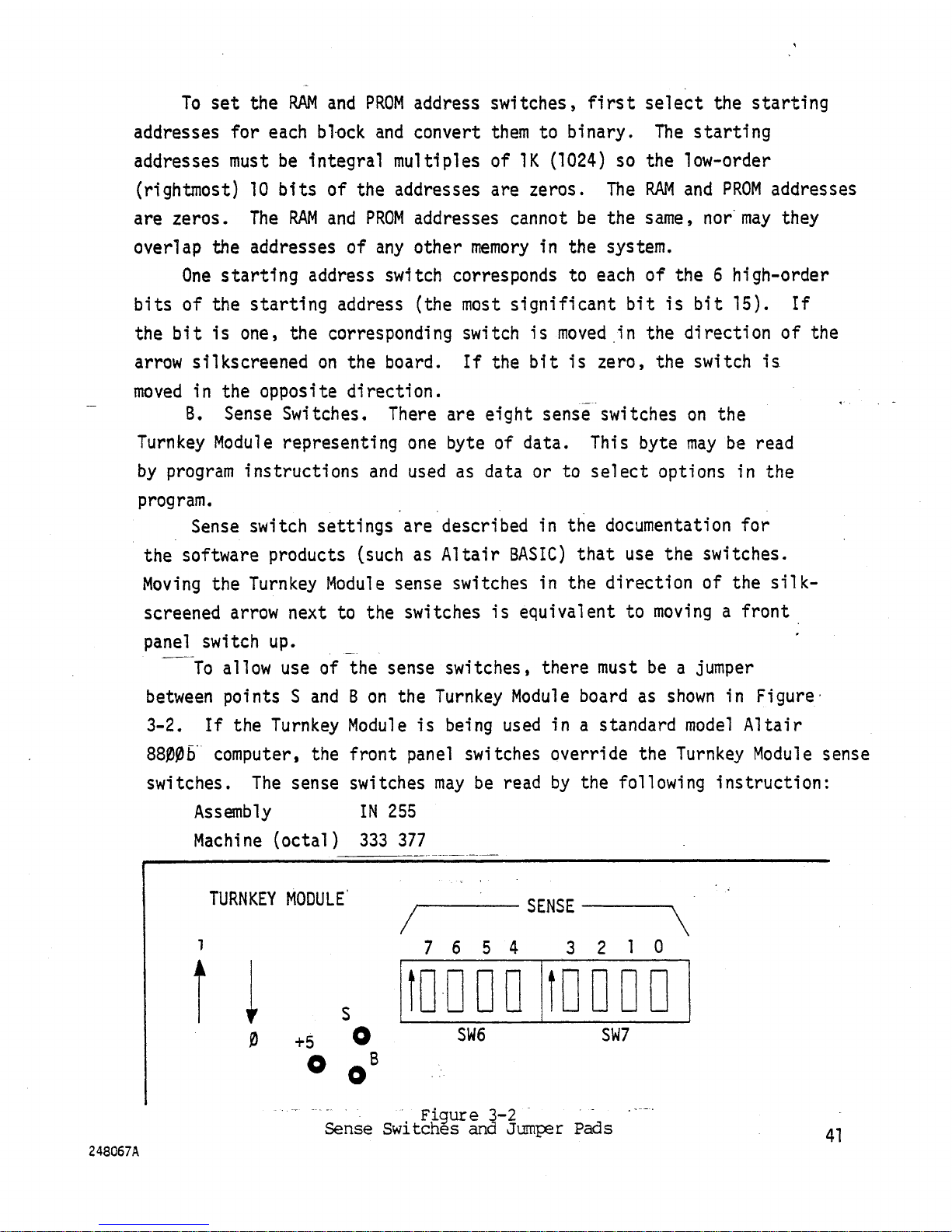
To set the RAM and PROM address switches, first select the starting
addresses for each block and convert them to binary. The starting
addresses must be integral multiples of IK (1024) so the low-order
(rightmost) 10 bits of the addresses are zeros. The RAM and PROM addresses
are zeros. The RAM and PROM addresses cannot be the same, nor may they
overlap the addresses of any other memory in the system.
One starting address switch corresponds to each of the 6 high-order
bits of the starting address (the most significant bit is bit 15). If
the bit is one, the corresponding switch is moved in the direction of the
arrow silkscreened on the board. If the bit is zero, the switch is
moved in the opposite direction.
B. Sense Switches. There are eight sense switches on the
Turnkey Module representing one byte of data. This byte may be read
by program instructions and used as data or to select options in the
program.
Sense switch settings are described in the documentation for
the software products (such as Altair BASIC) that use the switches.
Moving the Turnkey Module sense switches in the direction of the silk-
screened arrow next to the switches is equivalent to moving a front
panel switch up.
To allow use of the sense switches, there must be a jumper
between points S and B on the Turnkey Module board as shown in Figure
3-2. If the Turnkey Module is being used in a standard model Altair
88006 computer, the front panel switches override the Turnkey Module sense
switches. The sense switches may be read by the following instruction:
Assembly IN 255
Machine (octal) 333 377
1
1
f
0
. Figure 3-2
Sense Switches and Jumper Pads
EY MODULE
SENSE
7 6 5 4 3 2 1 0
+5
SW6 SW7
o
0
b
Page 52
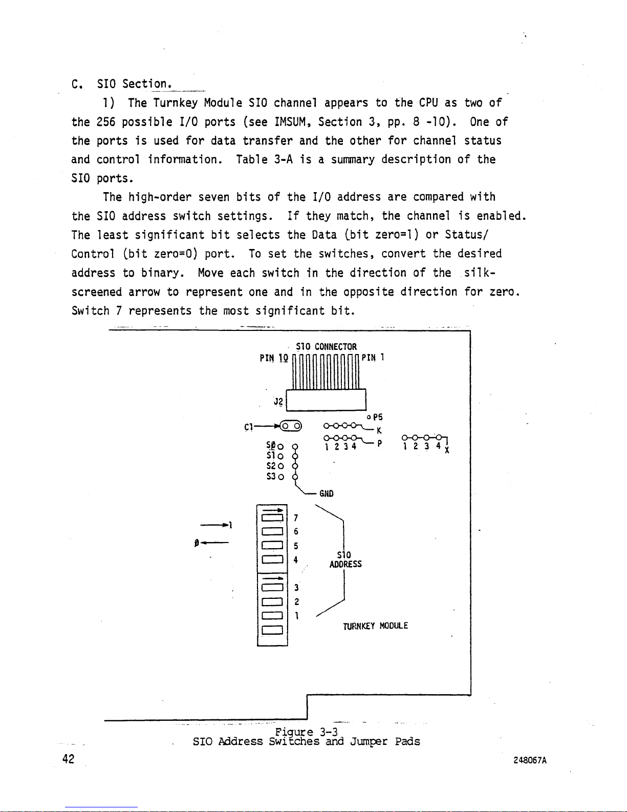
C. SIO Section.
1) The Turnkey Module SIO channel appears to the CPU as two of
the 256 possible I/O ports (see IMSUM, Section 3, pp. 8 -10). One of
the ports is used for data transfer and the other for channel status
and control information. Table 3-A is a summary description of the
SIO ports.
The high-order seven bits of the I/O address are compared with
the SIO address switch settings. If they match, the channel is enabled.
The least significant bit selects the Data (bit zero=l) or Status/
Control (bit zero=0) port. To set the switches, convert the desired
address to binary. Move each switch in the direction of the silkscreened arrow to represent one and in the opposite direction for zero.
Switch 7 represents the most significant bit.
SIO CONNECTOR
pin is nnnnnnnnnnpiN i
J2
oP5
K.
O-OOO-v n OO-O-O-j
1 2 3 4 P 1 2 3 4 i
SIO
AOORESS
TURNKEY MOOULE
42
Figure 3-3
SIO Address Switches and Jumper Pads
248067A
Page 53
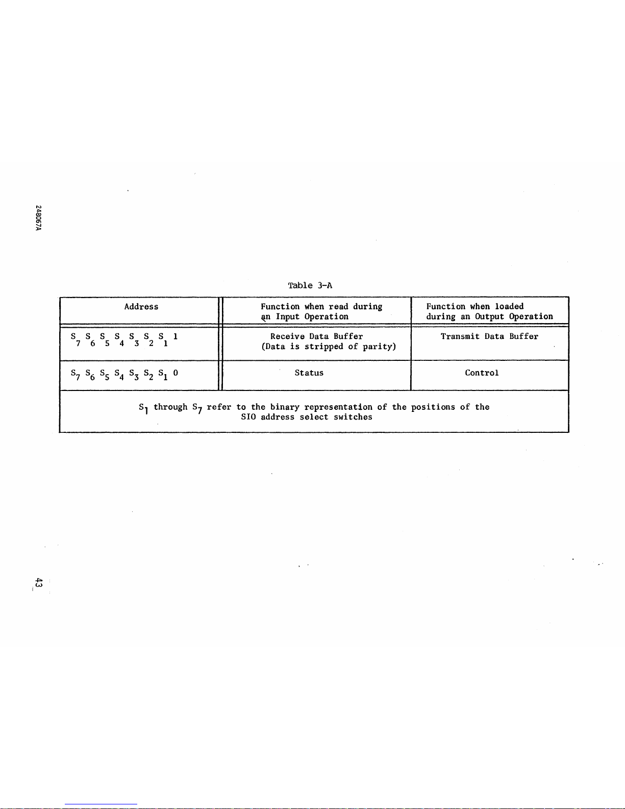
Table 3-A
Address
Function when read during
^n Input Operation
Function when loaded
during an Output Operation
SSSSSSSl
7 6 5 4 3 2 1
Receive Data Buffer
(Data is stripped of parity)
Transmit Data Buffer
S7 S6 S5 S4 S3 S2 S1 0
Status Control
S-j through Sy refer to the binary representation of the positions of the
SIO address select switches
Page 54
2) The Status Register. When the Status/Control port is read during
an input operation, the Status Register contains information on the status
of the Transmit Data Register, the Receive Data Register and error logic,
and the peripheral/modem status inputs. The function of each bit of the
status register is given in the table below.
a. Receive Data Register Full (RDRF), Bit 0. Receive Data Register
Full indicates that received data has been transferred to the Receive Data
Register. RDRF is cleared after the CPU reads the Receive Data Register or
by a master reset. The cleared or empty state indicates that the contents
of the Receive Data Register are not current. RDRF also indicates empty if
Data Carrier Detect is LOW.
b. Transmit Data Register Empty (TDRE), Bit 1. The Transmit Data Register Empty bit set to 1 indicates that the Transmit Data Register contents
have been transferred and that new data may be entered. A zero indicates that
the register is full and that transmission of a new character has not begun
since the last write data command.
c. Data Carrier Detect (DCD), Bit 2. When the DCD input from a modem
goes LOW to indicate that a carrier is not present, the Data Carrier Detect
bit is set to 1. This setting causes an Interrupt Request to be generated
if the Receive Interrupt Enable bit is set. After the DCD input returns HIGH,
DCD remains one until it is reset, either by reading first the Status Register
and then the Data Register, or by a master reset. If the DCD input remains
LOW after the Status and Data Registers have been read or a master reset occurs,
the DCD bit remains the inverse of the DCD input.
d. Clear-to-Send (CTS), Bit 3. The Clear-to-Send bit is the inverse
of the Clear-to-Send input from a modem. Thus, zero in CTS indicates that
there is a Clear-to-Send from the modem. When the Clear-to-Send signal is
LOW, the Transmit Data Register Empty bit is inhibited and the CTS" status
bit is set to one. Master reset does not affect the CTS bit.
e. Framing Error (FE), bit 4. A framing error occurs when the received
character is improperly framed by a start and a stop bit. It is detected
by the absence of the first stop bit. This indicates a synchronization error,
faulty transmission or a break condition. The Framing Error flag, FE, is
set during the receive data transfer time. Therefore, the error indicator
is present throughout the time that the associated character is available.
44
248067A
Page 55
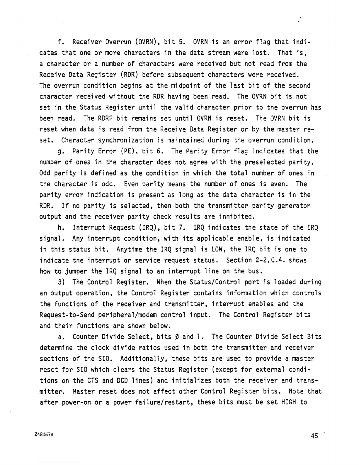
f. Receiver Overrun (OVRN), bit 5. OVRN is an error flag that indicates that one or more characters in the data stream were lost. That is,
a character or a number of characters were received but not read from the
Receive Data Register (RDR) before subsequent characters were received.
The overrun condition begins at the midpoint of the last bit of the second
character received without the RDR having been read. The OVRN bit is not
set in the Status Register until the valid character prior to the overrun has
been read. The RDRF bit remains set until OVRN is reset. The OVRN bit is
reset when data is read from the Receive Data Register or by the master reset. Character synchronization is maintained during the overrun condition.
g. Parity Error (PE), bit 6. The Parity Error flag indicates that the
number of ones in the character does not agree with the preselected parity.
Odd parity is defined as the condition in which the total number of ones in
the character is odd. Even parity means the number of ones is even. The
parity error indication is present as long as the data character is in the
RDR. If no parity is selected, then both the transmitter parity generator
output and the receiver parity check results are inhibited.
h. Interrupt Request (IRQ), bit 7. IRQ indicates the state of the IRQ
signal. Any interrupt condition, with its applicable enable, is indicated
in this status bit. Anytime the IRQ signal is LOW, the IRQ bit is one to
indicate the interrupt or service request status. Section 2-2.C.4. shows
how to jumper the IRQ signal to an interrupt line on the bus.
3) The Control Register. When the Status/Control port is loaded during
an output operation, the Control Register contains information which controls
the functions of the receiver and transmitter, interrupt enables and the
Request-to-Send peripheral/modem control input. The Control Register bits
and their functions are shown below.
a. Counter Divide Select, bits 0 and 1. The Counter Divide Select Bits
determine the clock divide ratios used in both the transmitter and receiver
sections of the SIO. Additionally, these bits are used to provide a master
reset for SIO which clears the Status Register (except for external conditions on the CTS and DCD lines) and initializes both the receiver and transmitter. Master reset does not affect other Control Register bits. Note that
after power-on or a power failure/restart, these bits must be set HIGH to
243067A
45
Page 56
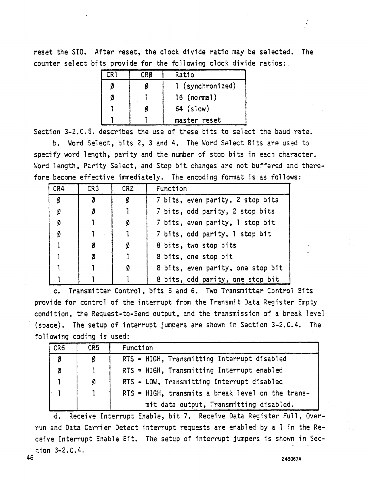
reset the SIO. After reset, the clock divide ratio may be selected. The
counter select bits provide for the following clock divide ratios:
CRT CR0 Ratio
0 0
1 (synchronized)
0
1
16 (normal)
1
0
64 (slow)
1 1 master reset
Section 3-2.C.5. describes the use of these bits to select the baud rate.
b. Word Select, bits 2, 3 and 4. The Word Select Bits are used to
specify word length, parity and the number of stop bits in each character.
Word length, Parity Select, and Stop bit changes are not buffered and therefore become effective immediately. The encoding format is as follows:
CR4 CR3
CR2
Function
0
0
0
7 bits, even parity, 2 stop bits
0
0
1 7 bits, odd parity, 2 stop bits
0
1
0
7 bits, even parity, 1 stop bit
0
1
1
7 bits, odd parity, 1 stop bit
1
0
0
8 bits, two stop bits
1
0
1
8 bits, one stop bit
1
1
0
8 bits, even parity, one stop bit
1 1
1 8 bits, odd parity, one stop bit
c. Transmitter Control, bits 5 and 6. Two Transmitter Control Bits
provide for control of the interrupt from the Transmit Data Register Empty
condition, the Request-to-Send output, and the transmission of a break level
(space). The setup of interrupt jumpers are shown in Section 3-2.C.4. The
following coding is used:
CR6 CR5 Function
0
0
RTS
= HIGH, Transmitting Interrupt disabled
0
1
RTS
= HIGH, Transmitting Interrupt enabled
1
0
RTS = LOW, Transmitting Interrupt disabled
1
1 RTS
= HIGH, transmits a break level on the trans-
mit data output, Transmitting disabled.
d. Receive Interrupt Enable, bit 7. Receive Data Register Full, Overrun and Data Carrier Detect interrupt requests are enabled by a 1 in the Receive Interrupt Enable Bit. The setup of interrupt jumpers is shown in Sec-
tion 3-2.C.4.
46 248067A
Page 57
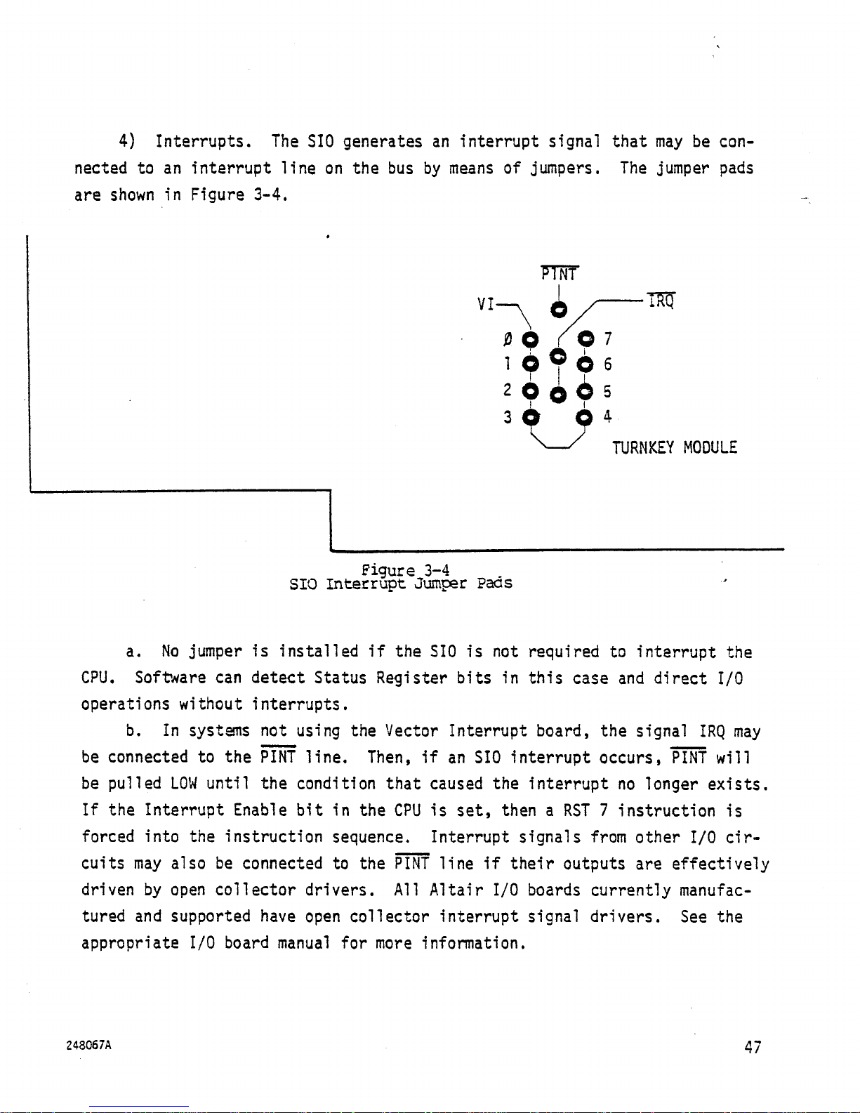
4) Interrupts. The SIO generates an interrupt signal that may be connected to an interrupt line on the bus by means of jumpers. The jumper pads
are shown in Figure 3-4.
mr
1/ TScT
0 O r O 7
??5
6
2 O o ^
5
3
0
4
N
—' TURNKEY MODULE
Figure 3-4
SIO Interrupt Jumper Pads
a. No jumper is installed if the SIO is not required to interrupt the
CPU. Software can detect Status Register bits in this case and direct I/O
operations without interrupts.
b. In systems not using the Vector Interrupt board, the signal IRQ may
be connected to the PINT line. Then, if an SIO interrupt occurs, PINT will
be pulled LOW until the condition that caused the interrupt no longer exists.
If the Interrupt Enable bit in the CPU is set, then a RST 7 instruction is
forced into the instruction sequence. Interrupt signals from other I/O circuits may also be connected to the PINT line if their outputs are effectively
driven by open collector drivers. All Altair I/O boards currently manufac-
tured and supported have open collector interrupt signal drivers. See the
appropriate I/O board manual for more information.
248067A
47
Page 58
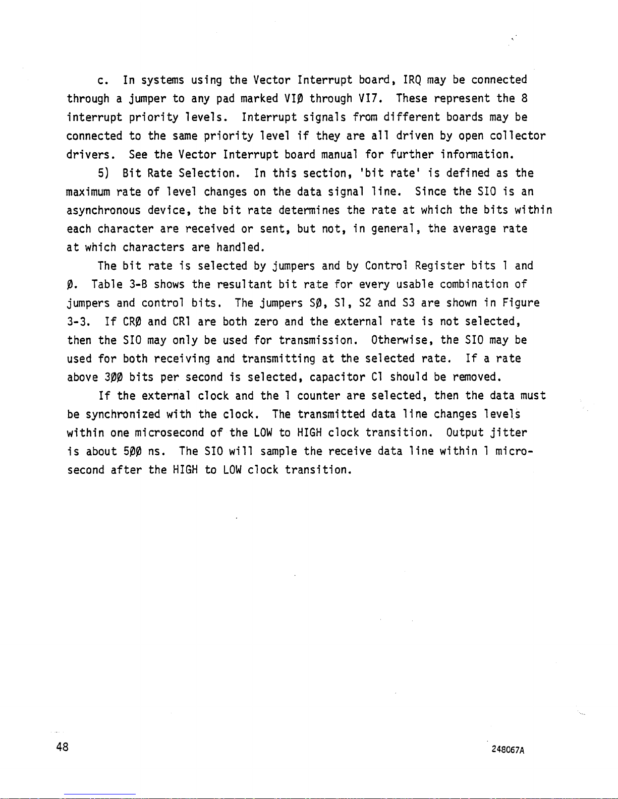
c. In systems using the Vector Interrupt board, IRQ may be connected
through a jumper to any pad marked VI0 through VI7. These represent the 8
interrupt priority levels. Interrupt signals from different boards may be
connected to the same priority level if they are all driven by open collector
drivers. See the Vector Interrupt board manual for further information.
5) Bit Rate Selection. In this section, 'bit rate1 is defined as the
maximum rate of level changes on the data signal line. Since the SIO is an
asynchronous device, the bit rate determines the rate at which the bits within
each character are received or sent, but not, in general, the average rate
at which characters are handled.
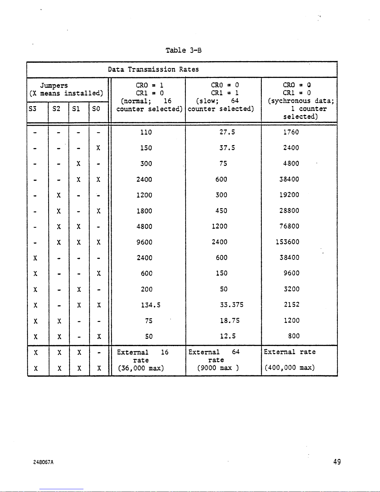
The bit rate is selected by jumpers and by Control Register bits 1 and
0. Table 3-B shows the resultant bit rate for every usable combination of
jumpers and control bits. The jumpers S0, SI, S2 and S3 are shown in Figure
3-3. If CR0 and CRT are both zero and the external rate is not selected,
then the SIO may only be used for transmission. Otherwise, the SIO may be
used for both receiving and transmitting at the selected rate. If a rate
above 300 bits per second is selected, capacitor CI should be removed.
If the external clock and the 1 counter are selected, then the data must
be synchronized with the clock. The transmitted data line changes levels
within one microsecond of the LOW to HIGH clock transition. Output jitter
is about 500 ns. The SIO will sample the receive data line within 1 microsecond after the HIGH to LOW clock transition.
48
248067A
Page 59
Jumpers
(X
means installed)
S3 S2 SI so
Table
3-B
Data Transmission Rates
CRO = 1
CRO = 1
CRl = 0
CRl = 0
(normal;
(normal;
counter selected)
counter selected)
16
16
(slow;
(slow;
counter selected)
counter selected)
CRO = 0
CRO = 0
CRl = 1
CRl = 1
64
64
CRO = 0
CRO = 0
CRl = 0
CRl = 0
(sychronous data;
(sychronous data;
1
counter
1
counter
selected)
selected)
-
- -
-
- -
-
-
- X
-
X
X
X
X
-
-
X
X
X
-
-
- X
-
-
-
X
-
X
-
X X
-
-
X
X
-
-
X
^
X
-
X
-
X
-
X 134.5
110
150
300
2400
1200
1800
4800
9600
2400
600
200
27.5
37.5
75
600
300
450
1200
2400
600
150
50
33.375
1760
2400
4800
38400
19200
28800
76800
153600
38400
9600
3200
2152
X X
X X
X
X
248067A
X
X X X
-
-
-
X 50
External
X
(36,000
75
rate
max)
16
External
rate
(9000
18.75
12.5
64
max )
1200
800
External rate
(400,000
max)
49
Page 60
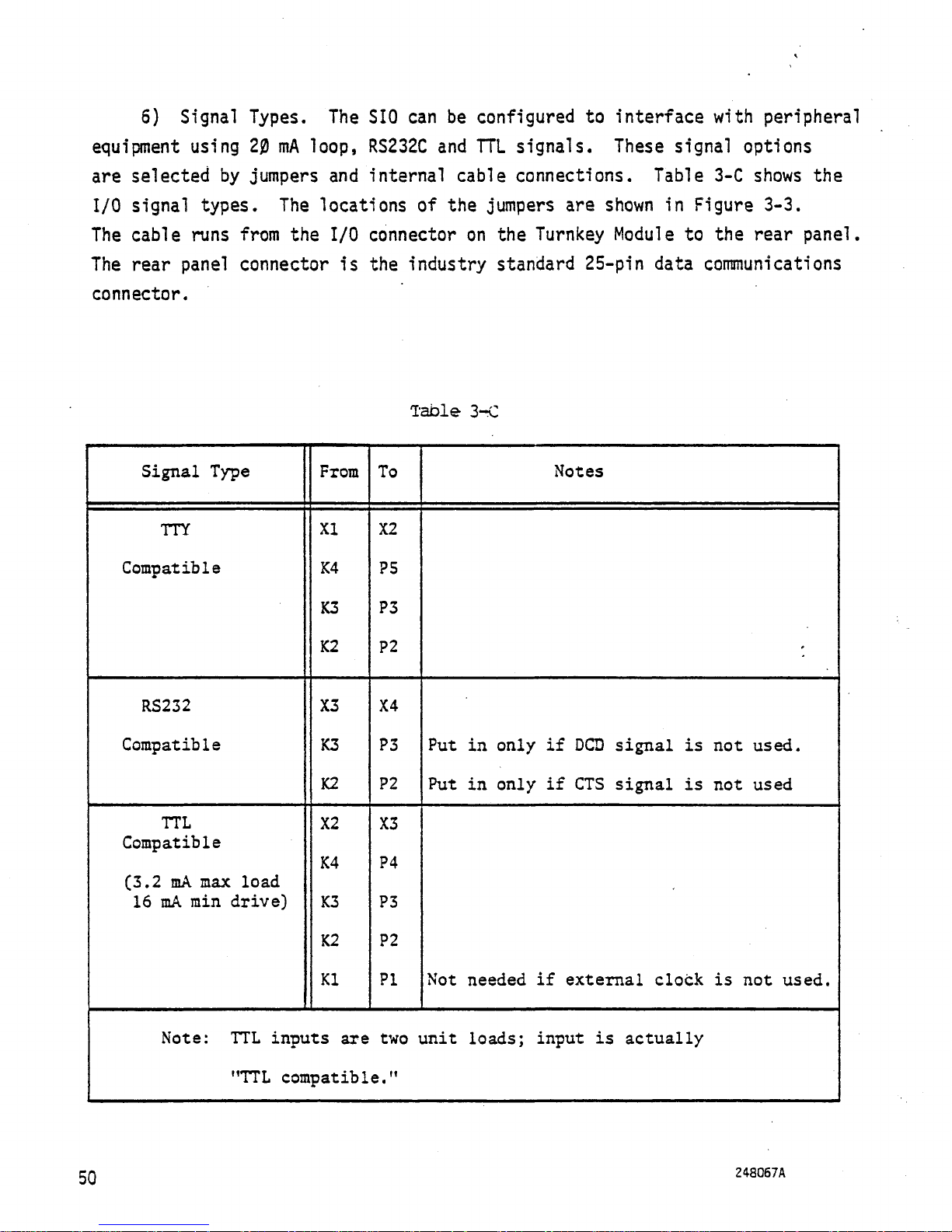
6) Signal Types. The SIO can be configured to interface with peripheral
equipment using 20 mA loop, RS232C and TTL signals. These signal options
are selected by jumpers and internal cable connections. Table 3-C shows the
I/O signal types. The locations of the jumpers are shown in Figure 3-3.
The cable runs from the I/O connector on the Turnkey Module to the rear panel.
The rear panel connector is the industry standard 25-pin data communications
connector.
Table 3-C
Signal Type From To
Notes
TTY
Compatible
XI
K4
K3
K2
X2
P5
P3
P2
RS232
Compatible
X3
K3
K2
X4
P3
P2
Put in only if DCD signal is not used.
Put in only if CTS signal is not used
TTL
Compatible
(3.2 mA max load
16 mA min drive)
X2
K4
K3
K2
K1
X3
P4
P3
P2
PI
Not needed if external clock is not used.
Note: TTL inputs are two unit loads; input is actually
"TTL compatible."
50
248067A
Page 61
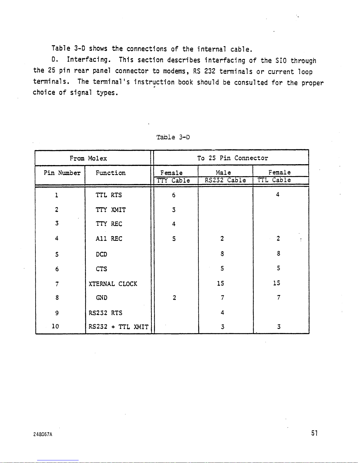
Table 3-D shows the connections of the internal cable.
D. Interfacing. This section describes interfacing of the SIO through
the 25 pin rear panel connector to modems, RS 232 terminals or current loop
terminals. The terminal's instruction book should be consulted for the proper
choice of signal types.
Table 3-D
From Molex
To 25 Pin Connector
Pin Number Function Female
Male
Female
Pin Number Function
TTY Cable
RS232 Cable
TTL Cable
1
TTL RTS 6
4
2
TTY XMIT 3
3
TTY REC
4
4
All REC
5
2
2
5
DCD
8
8
6
CTS
5
5
7 XTERNAL CLOCK
15
15
8 GND
2
7
7
9
RS232 RTS
4
10
RS232 + TTL XMIT
3
3
243G67A
51
Page 62
1) Connection to a modem is through a male to female extension cable.
The board and internal cable are set up for RS-232 I/O.
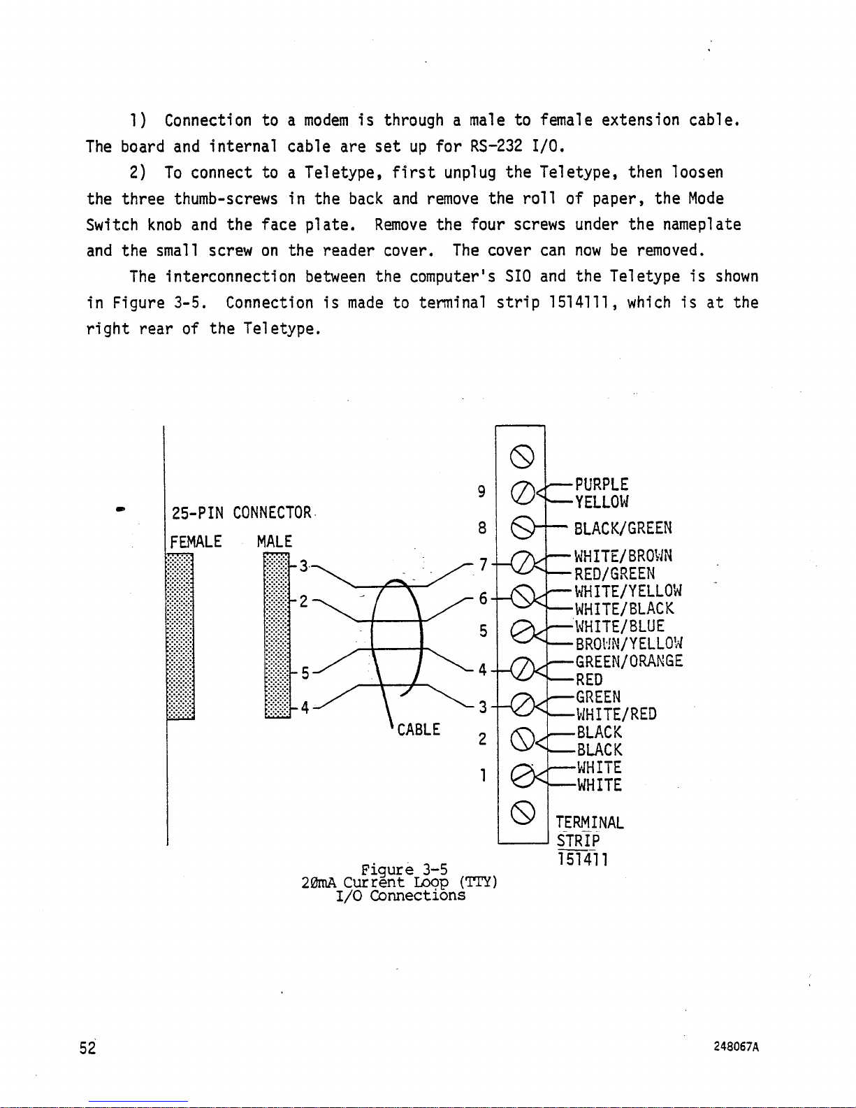
2) To connect to a Teletype, first unplug the Teletype, then loosen
the three thumb-screws in the back and remove the roll of paper, the Mode
Switch knob and the face plate. Remove the four screws under the nameplate
and the small screw on the reader cover. The cover can now be removed.
The interconnection between the computer's SIO and the Teletype is shown
in Figure 3-5. Connection is made to terminal strip 1514111, which is at the
right rear of the Teletype.
®
n\\—PURPLE
25-PIN CONNECTOR
FEMALE MALE
CABLE
I/TV—WHITE/BROWN
7
/CV'—WHITE/YELLOW
fi
_L0<'—
4
3f0d
—YELLOW
Q BLACK/GREEN
—RED/GREEN
WHITE/BLACK
£V—WHITE/BLUE
—BROWN/YELLOW
GREEN/QRANG£
•RED
-GREEN
-WHITE/RED
-BLACK
•BLACK
WHITE
—
WHITE
52
20mA Current Loop (TTY)
Figure 3-5
I/O Connections
0 TERMINAL
STRIP
151411
248067A
Page 63
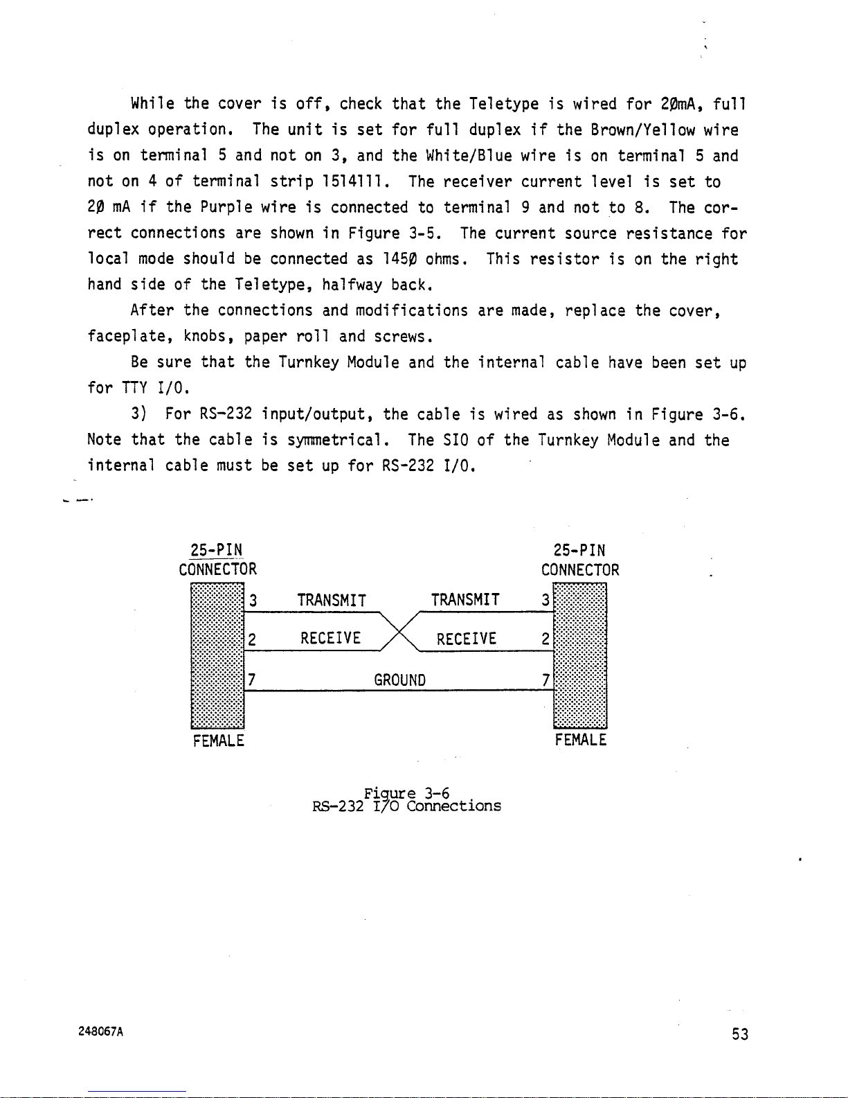
While the cover is off, check that the Teletype is wired for 20mA, full
duplex operation. The unit is set for full duplex if the Brown/Yellow wire
is on terminal 5 and not on 3, and the White/Blue wire is on terminal 5 and
not on 4 of terminal strip 1514111. The receiver current level is set to
20 mA if the Purple wire is connected to terminal 9 and not to 8. The correct connections are shown in Figure 3-5. The current source resistance for
local mode should be connected as 1450 ohms. This resistor is on the right
hand side of the Teletype, halfway back.
After the connections and modifications are made, replace the cover,
faceplate, knobs, paper roll and screws.
Be sure that the Turnkey Module and the internal cable have been set up
for TTY I/O.
3) For RS-232 input/output, the cable is wired as shown in Figure 3-6.
Note that the cable is symmetrical. The SIO of the Turnkey Module and the
internal cable must be set up for RS-232 I/O.
25-PIN
CONNECTOR
3 TRANSMIT
2 RECEIVE
7
FEMALE
25-PIN
CONNECTOR
TRANSMIT 3
RECEIVE 2
GROUND 7
FEMALE
Figure 3-6
RS-232 I/O Connections
248067A
53
Page 64
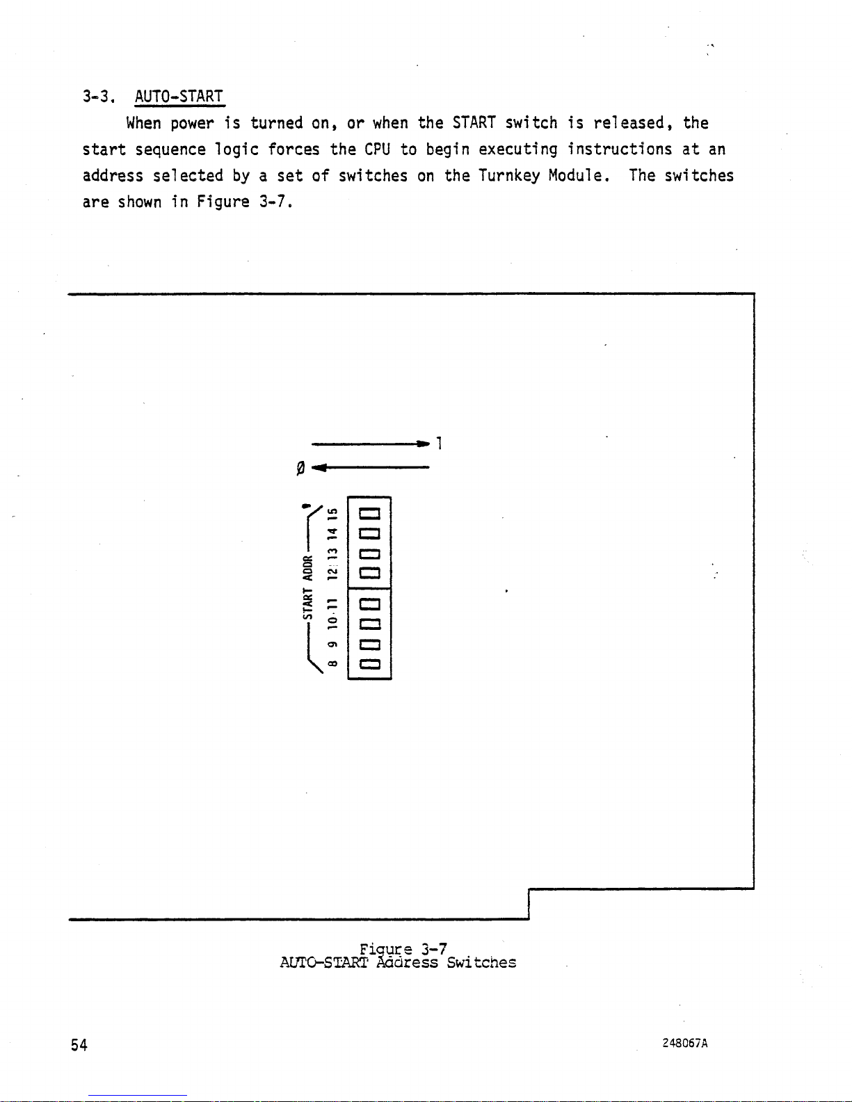
3-3. AUTO-START
When power is turned on, or when the START switch is released, the
start sequence logic forces the CPU to begin executing instructions at an
address selected by a set of switches on the Turnkey Module. The switches
are shown in Figure 3-7.
D
•
CZJ
•
•
a
a
CD
1
Figure 3-7
AUTO-START Address Switches
54
248067A
Page 65
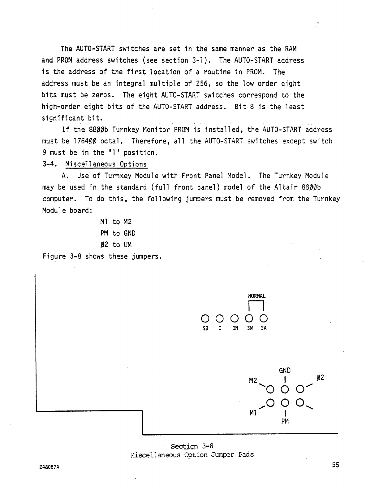
The AUTO-START switches are set in the same manner as the RAM
and PROM address switches (see section 3-1)- The AUTO-START address
is the address of the first location of a routine in PROM. The
address must be an integral multiple of 256, so the low order eight
bits must be zeros. The eight AUTO-START switches correspond to the
high-order eight bits of the AUTO-START address. Bit 8 is the least
significant bit.
If the 8800b Turnkey Monitor PROM is installed, the AUTO-START address
must be 176400 octal. Therefore, all the AUTO-START switches except switch
9 must be in the
11
1" position.
3-4. Miscellaneous Options
A. Use of Turnkey Module with Front Panel Model. The Turnkey Module
may be used in the standard (full front panel) model of the Altair 8800b
computer. To do this, the following jumpers must be removed from the Turnkey
Module board:
Ml to M2
PM to GND
02 to UM
Figure 3-8 shows these jumpers.
NORMAL
n
o o o o o
SB C ON SW SA
GND
M2 I
^O o o"
^O o o^
Ml |
PM
248067A
Section 3-8
Miscellaneous Option Jumper Pads
55
Page 66
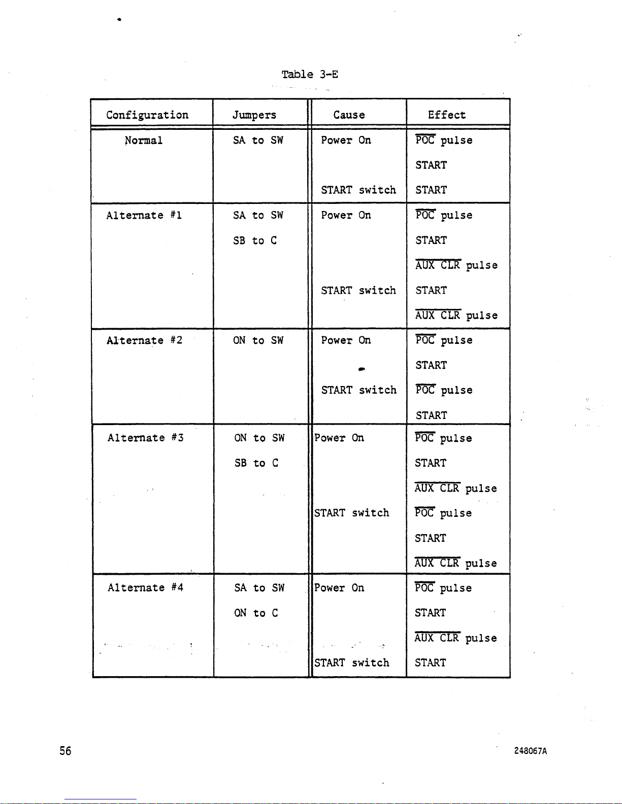
Table 3-E
Configuration Jumpers Cause Effect
formal
SA to SW
Power On
START switch
POC pulse
START
START
Alternate #1
SA to SW
SB to C
Power On
START switch
PoS" pulse
START
Alternate #1
SA to SW
SB to C
Power On
START switch
AUX CLR pulse
START
Alternate #1
SA to SW
SB to C
Power On
START switch
AUX CLR pulse
Alternate #2
ON to SW
Power On
START switch
POC pulse
START
PoiT pulse
START
Alternate #3 ON to SW
SB to C
Power On
START switch
POC" pulse
START
Alternate #3 ON to SW
SB to C
Power On
START switch
AUX CLR pulse
POC pulse
START
Alternate #3 ON to SW
SB to C
Power On
START switch
AUX CLR pulse
Alternate #4
SA to SW
ON to C
Power On
START switch
POC pulse
START
Alternate #4
SA to SW
ON to C
Power On
START switch
AUX CLR pulse
START
56
248067A
Page 67
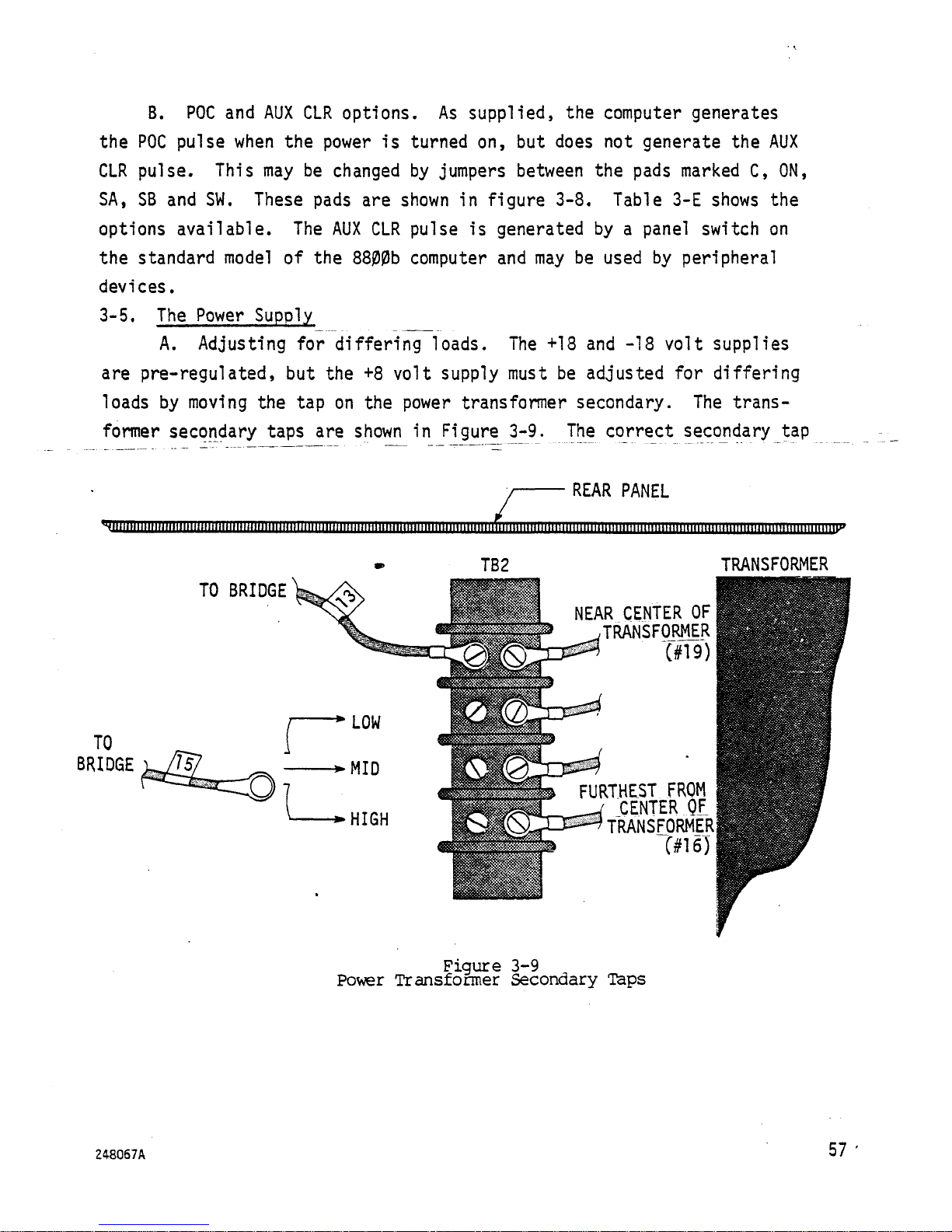
B. POC and AUX CLR options. As supplied, the computer generates
the POC pulse when the power is turned on, but does not generate the AUX
CLR pulse. This may be changed by jumpers between the pads marked C, ON,
SA, SB and SW. These pads are shown in figure 3-8. Table 3-E shows the
options available. The AUX CLR pulse is generated by a panel switch on
the standard model of the 8800b computer and may be used by peripheral
devices.
3-5. The Power Supply
A. Adjusting for differing loads. The +18 and -18 volt supplies
are pre-regulated, but the +8 volt supply must be adjusted for differing
loads by moving the tap on the power transformer secondary. The transformer secondary taps are shown in Figure 3-9. The correct secondary tap
REAR PANEL
IIIIIIllllllllllillllillllilllllllllilllllllllllllllllllllllllllMlllillllllllllllllllllllllHllimillll ITTIi
iiiiHHiiintiiiiiiHiiiHiiini)^
TO BRIDGE
TO
BRIDGE
TRANSFORMER
NEAR CENTER OF
TRANSFORMER
'(#19)
FURTHEST FROM
CENTER QF
TRANSFORMER
C#16)
Figure 3-9
Power Transformer Secondary Taps
248067A
57
Page 68
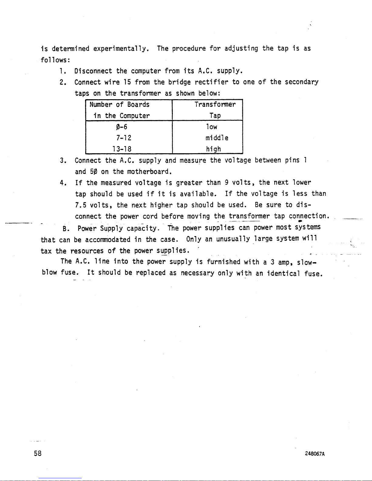
is determined experimentally. The procedure for adjusting the tap is as
follows:
1. Disconnect the computer from its A.C. supply.
2. Connect wire 15 from the bridge rectifier to one of the secondary
taps on the transformer as shown below:
Number of Boards
Transformer
in the Computer
Tap
0-6
low
7-12
middle
13-18
high
3. Connect the A.C. supply and measure the voltage between pins 1
and 50 on the motherboard.
4. If the measured voltage is greater than 9 volts, the next lower
tap should be used if it is available. If the voltage is less than
7.5 volts, the next higher tap should be used. Be sure to dis-
connect the power cord before moving the transformer tap connection.
B. Power Supply capacity. The power supplies can power most systems
that can be accommodated in the case. Only an unusually large system will
tax the resources of the power supplies.
The A.C. line into the power supply is furnished with a 3 amp, slow-
blow fuse. It should be replaced as necessary only with an identical fuse.
58 248067A
Page 69

248067A
59/(60 Blank)
Page 70

Page 71
4. TROUBLESHOOTING HINTS
4-1. Introduction
This section is not an extensive troubleshooting guide, but rather
contains guidelines that can save the troubleshooter time. Knowledge of
electronics and of the contents of Sections 2 and 3 of this manual is required
for troubleshooting.
A, Equipment. An oscilloscope with 30 MHz or greater bandwidth is
normally required to troubleshoot this unit. A voltage meter may be required
in some measurements. In most cases, either a logic analyzer or a full
panel version of the Altair 8800b computer is also needed. If the Turnkey
Module is used with the front panel, remove jumpers as described in para-
graph 3-9. To display both address lines and data lines on the logic analyzer,
clock on the falling edge of IC W pin 8 on the Turnkey Module. To view data
going to the Data Out bus as well as the Data In bus, make connections to
the bi-direction bus on the CPU board.
B, Troubleshooting Optional Boards. Troubleshooting optional memory
and I/O boards is covered in the manuals for those boards. The directions
in these manuals often assume that a full front panel is used, presenting
test loops to be executed in the single step mode. If a full front panel
is not used, use a logic analyzer and a test program instead.
C, Trouble Follows Change. An error in system change, jumper installation, repair or board modification can cause trouble. If a system change
has been made, be sure that all Turnkey Module jumpers are installed as shown
in Section 3. If boards were added, be sure that the +8 volt bus has the
correct voltage. Check that all boards and connectors are well seated and
mated correctly. If the trouble follows jumper installation, repair or
board modification, check for solder bridges and poor solder connections.
If the trouble follows repair, check that the IC pins were inserted into
the sockets properly.
4-2. Preliminary Considerations
A great deal of time can be saved by some preliminary checks.
A. First, check that all connectors and boards are well seated, that
the unit is plugged in and that the fuse is not open.
248067A
61
Page 72
B. Corner the problem by removing boards from the unit and by swapping
boards with good ones, if possible. Use this method with caution; a board
with a damaged bus driver may look OK when a good board is removed from the
system, because the load is reduced. If a board fails catastrophically,
several boards may be damaged along with cabling and power wiring. In
this case, each board should be tested in another system.
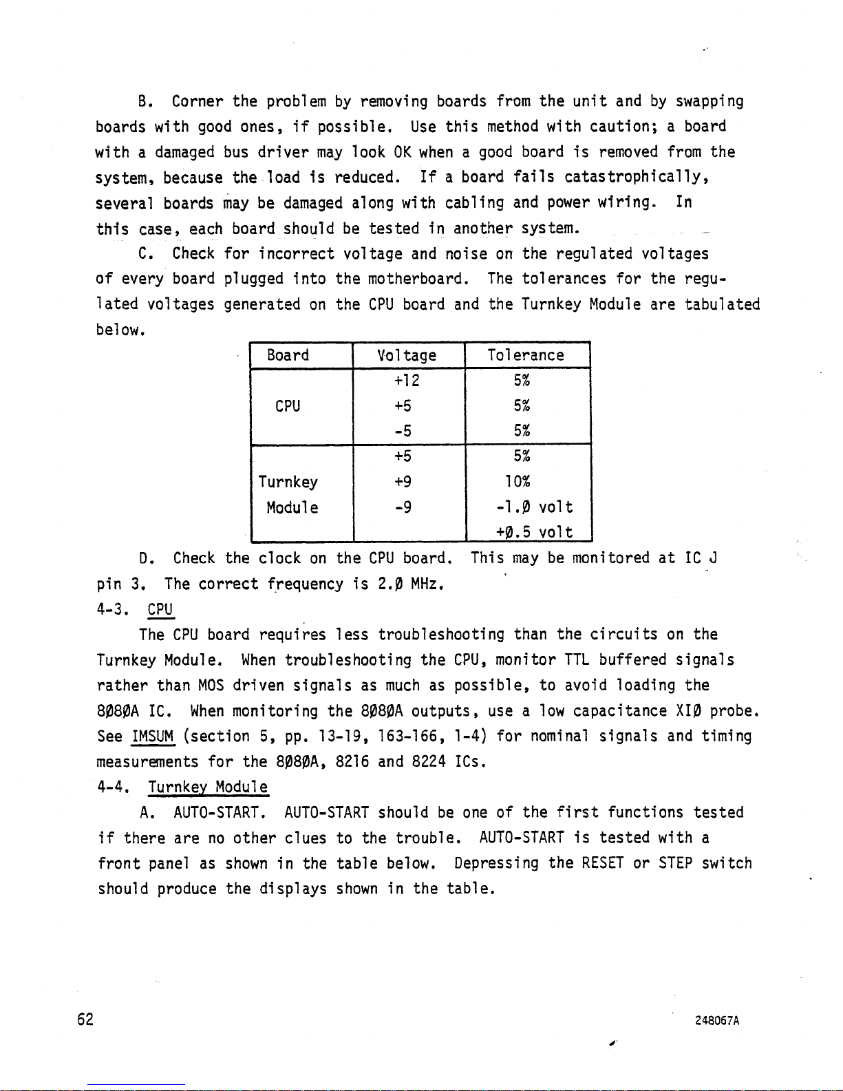
C. Check for incorrect voltage and noise on the regulated voltages
of every board plugged into the motherboard. The tolerances for the regu-
lated voltages generated on the CPU board and the Turnkey Module are tabulated
below.
Board Voltage Tolerance
+12
5%
CPU +5
5%
-5
5%
+5
5%
Turnkey
+9
10%
Module
-9
-1.0 volt
+0.5 volt
D. Check the clock on the CPU board. This may be monitored at IC 0
pin 3. The correct frequency is 2.0 MHz.
4-3. CPU
The CPU board requires less troubleshooting than the circuits on the
Turnkey Module. When troubleshooting the CPU, monitor TTL buffered signals
rather than MOS driven signals as much as possible, to avoid loading the
8080A IC. When monitoring the 8080A outputs, use a low capacitance XI0 probe.
See IMSUM (section 5, pp. 13-19, 163-166, 1-4) for nominal signals and timing
measurements for the 8080A, 8216 and 8224 ICs.
4-4. Turnkey Module
A. AUTO-START. AUTO-START should be one of the first functions tested
if there are no other clues to the trouble. AUTO-START is tested with a
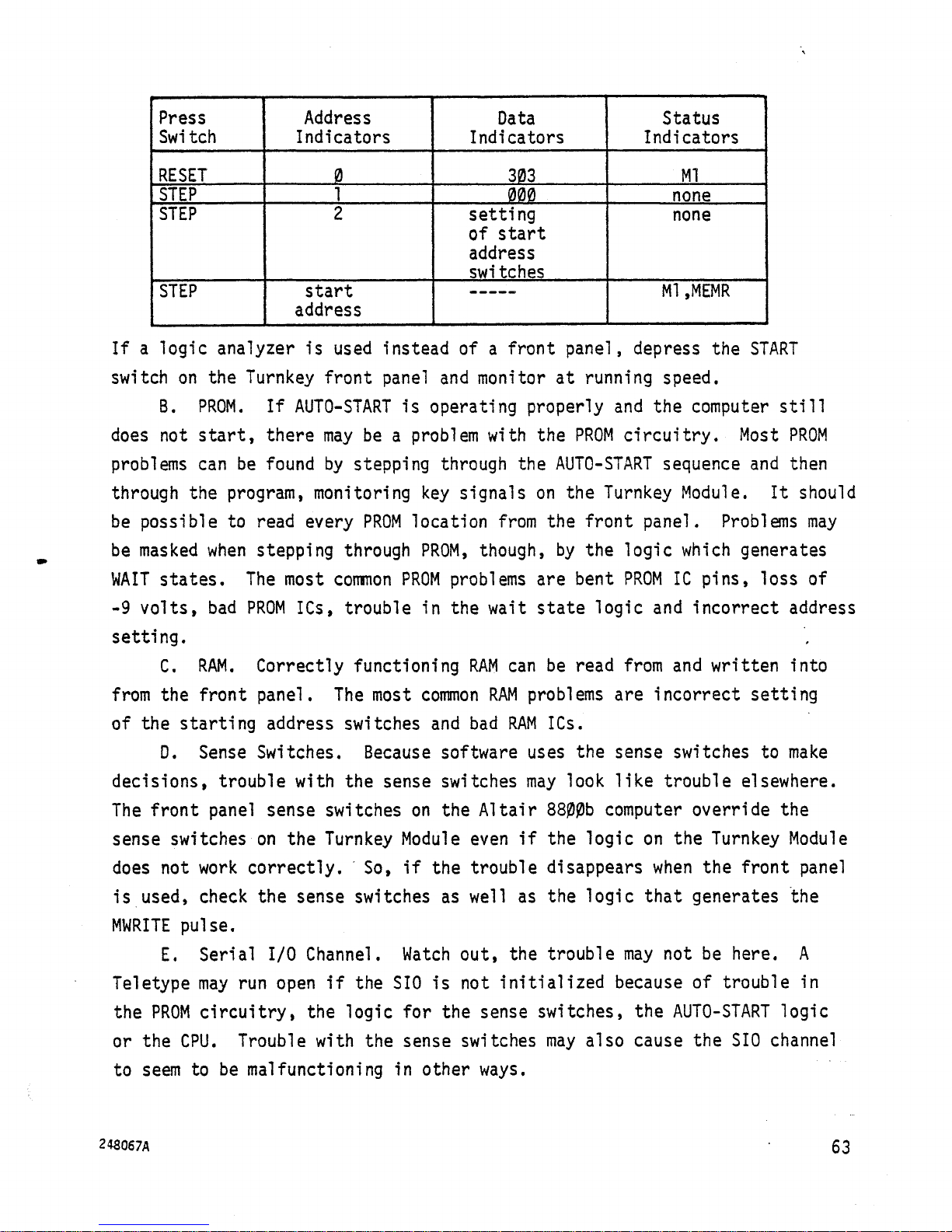
front panel as shown in the table below. Depressing the RESET or STEP switch
should produce the displays shown in the table.
62
248067A
Page 73
Press
Swi tch
Address
Indicators
Data
Indicators
Status
Indicators
RESET
0
303
Ml
STEP
1
000
none
STEP
2
setting
of start
address
switches
none
STEP start
address
—————
Ml ,MEMR
If a logic analyzer is used instead of a front panel, depress the START
switch on the Turnkey front panel and monitor at running speed.
B. PROM. If AUTO-START is operating properly and the computer still
does not start, there may be a problem with the PROM circuitry. Most PROM
problems can be found by stepping through the AUTO-START sequence and then
through the program, monitoring key signals on the Turnkey Module. It should
be possible to read every PROM location from the front panel. Problems may
be masked when stepping through PROM, though, by the logic which generates
WAIT states. The most common PROM problems are bent PROM IC pins, loss of
-9 volts, bad PROM ICs, trouble in the wait state logic and incorrect address
setting.
C. RAM. Correctly functioning RAM can be read from and written into
from the front panel. The most common RAM problems are incorrect setting
of the starting address switches and bad RAM ICs.
D. Sense Switches. Because software uses the sense switches to make
decisions, trouble with the sense switches may look like trouble elsewhere.
The front panel sense switches on the Altair 8800b computer override the
sense switches on the Turnkey Module even if the logic on the Turnkey Module
does not work correctly. So, if the trouble disappears when the front panel
is used, check the sense switches as well as the logic that generates the
MWRITE pulse.
E. Serial I/O Channel. Watch out, the trouble may not be here. A
Teletype may run open if the SIO is not initialized because of trouble in
the PROM circuitry, the logic for the sense switches, the AUTO-START logic
or the CPU. Trouble with the sense switches may also cause the SIO channel
to seem to be malfunctioning in other ways.
248067A
63
Page 74
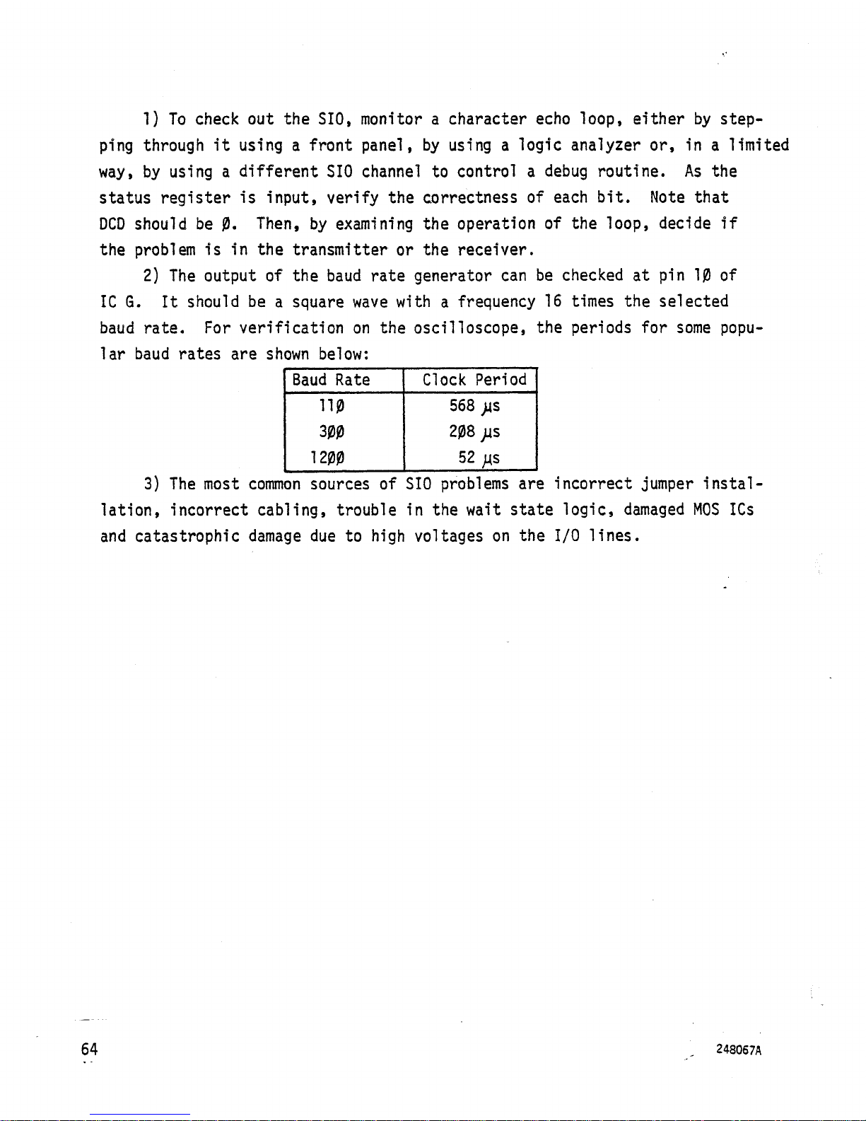
1) To check out the SIO, monitor a character echo loop, either by step-
ping through it using a front panel, by using a logic analyzer or, in a limited
way, by using a different SIO channel to control a debug routine. As the
status register is input, verify the correctness of each bit. Note that
DCD should be 0. Then, by examining the operation of the loop, decide if
the problem is in the transmitter or the receiver.
2) The output of the baud rate generator can be checked at pin 10 of
IC G. It should be a square wave with a frequency 16 times the selected
baud rate. For verification on the oscilloscope, the periods for some popular baud rates are shown below:
Baud Rate
Clock Period
110
568 ^s
300
208
)is
1200
52 us
3) The most common sources of SIO problems are incorrect jumper instal-
lation, incorrect cabling, trouble in the wait state logic, damaged MOS ICs
and catastrophic damage due to high voltages on the I/O lines.
64
248067A
Page 75

248067A
65/(60 Blank)
Page 76

Page 77

rarafnimnM
.1. JqUU JUUUUP
.
248067A
67/(60 Blank)
Page 78

Page 79
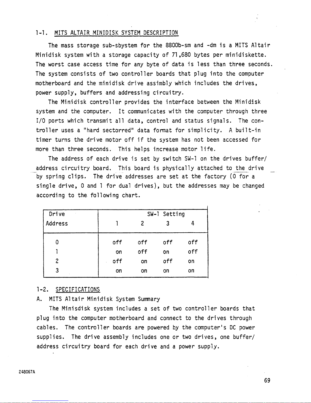
1-1. MITS ALTAIR MINIDISK SYSTEM DESCRIPTION
The mass storage sub-sbystem for the 8800b-sm and -dm is a MITS Altair
Minidisk system with a storage capacity of 71,680 bytes per minidiskette.
The worst case access time for any byte of data is less than three seconds.
The system consists of two controller boards that plug into the computer
motherboard and the minidisk drive assimbly which includes the drives,
power supply, buffers and addressing circuitry.
The Minidisk controller provides the interface between the Minidisk
system and the computer. It communicates with the computer through three
I/O ports which transmit all data, control and status signals. The controller uses a "hard sectorred" data format for simplicity. A built-in
timer turns the drive motor off if the system has not been accessed for
more than three seconds. This helps increase motor life.
The address of each drive is set by switch SW-1 on the drives buffer/
address circuitry board. This board is physically attached to the drive
by spring clips. The drive addresses are set at the factory (0 for a
single drive, 0 and 1 for dual drives), but the addresses may be changed
according to the following chart.
Dri
ve
SW-1
Setting
Address
1 2
3
4
0
off
off
off
off
1
on off on
off
2
off on off
on
3
on on
on
on
1-2. SPECIFICATIONS
A. MITS Altair Minidisk System Summary
The Minisdisk system includes a set of two controller boards that
plug into the computer motherboard and connect to the drives through
cables. The controller boards are powered by the computer's DC power
supplies. The drive assembly includes one or two drives, one buffer/
address circuitry board for each drive and a power supply.
248067A '
69
Page 80
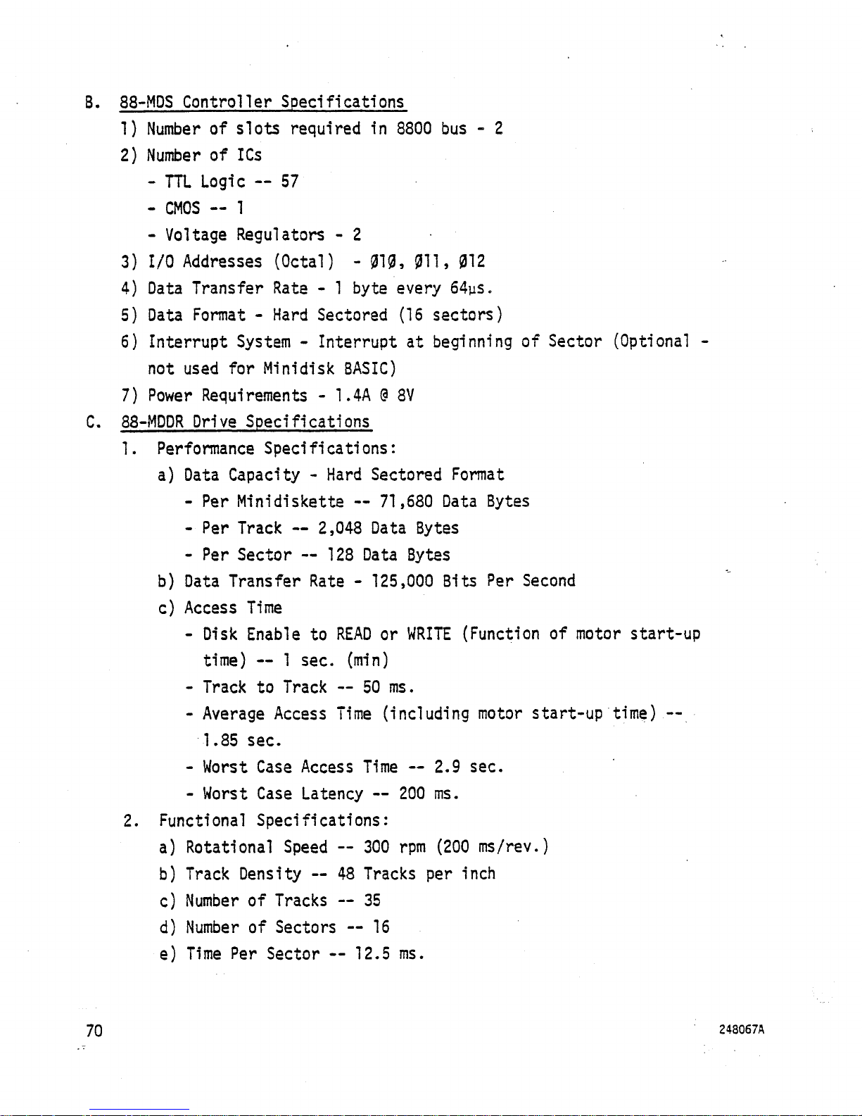
B. 88-MDS Controller Specifications
1) Number of slots required in 8800 bus - 2
2) Number of ICs
- TTL Logic — 57
- CMOS — 1
- Voltage Regulators - 2
3) I/O Addresses (Octal) - 010, 011, 012
4) Data Transfer Rate - 1 byte every 64us.
5) Data Format - Hard Sectored (16 sectors)
6) Interrupt System - Interrupt at beginning of Sector (Optional not used for Minidisk BASIC)
7) Power Requirements - 1.4A @ 8V
C. 88-MDDR Drive Specifications
1. Performance Specifications:
a) Data Capacity - Hard Sectored Format
- Per Minidiskette — 71,680 Data Bytes
- Per Track — 2,048 Data Bytes
- Per Sector — 128 Data Bytes
b) Data Transfer Rate - 125,000 Bits Per Second
c) Access Time
- Disk Enable to READ or WRITE (Function of motor start-up
time) — 1 sec. (min)
- Track to Track — 50 ms.
- Average Access Time (including motor start-up time) —
1.85 sec.
- Worst Case Access Time — 2.9 sec.
- Worst Case Latency — 200 ms.
2. Functional Specifications:
a) Rotational Speed ~ 300 rpm (200 ms/rev.)
b) Track Density — 48 Tracks per inch
c) Number of Tracks — 35
d) Number of Sectors — 16
e) Time Per Sector — 12.5 ms.
70
248067A
Page 81
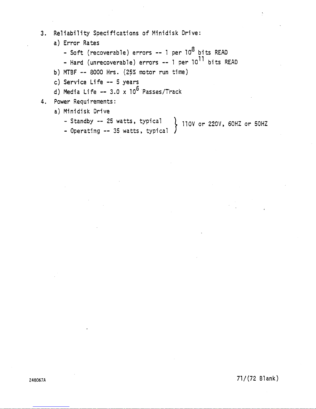
3. Reliability Specifications of Minidisk Drive:
a) Error Rates
g
- Soft (recoverable) errors — 1 per 10 bits READ
- Hard (unrecoverable) errors — 1 per 10^ bits READ
b) MTBF — 8000 Hrs. (2535 motor run time)
c) Service Life — 5 years
d) Media Life — 3.0 x 10⁶ Passes/Track
4. Power Requirements:
a) Minidisk Drive
- Standby - 25 watts, typical )
mv or 22QV> 6QHZ Qr 5QHZ
- Operating — 35 watts, typical )
248067A
71/(60 Blank)
Page 82

Page 83

crp
nn
i
fPTFninnn
b
m en? ®?
UJ
(L
248067A
73/(60 Blank)
Page 84

Page 85
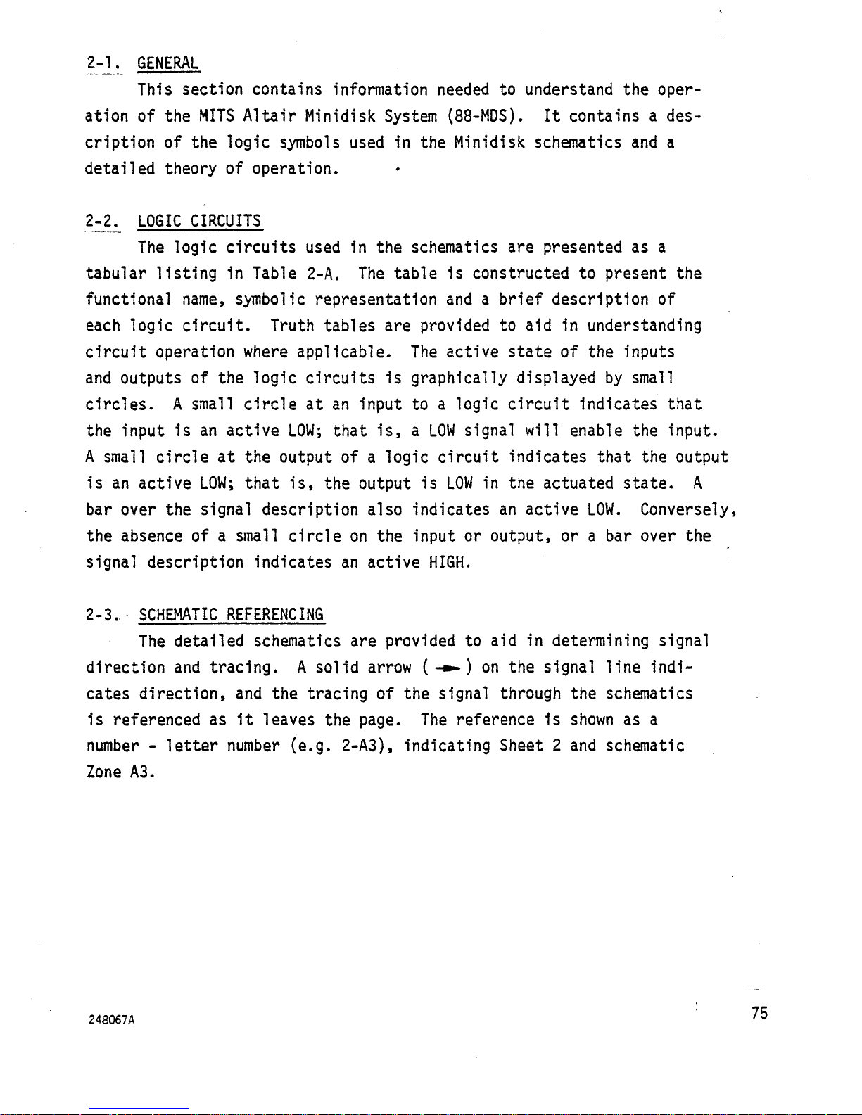
2-1. GENERAL
This section contains information needed to understand the operation of the MITS Altair Minidisk System (88-MDS). It contains a description of the logic symbols used in the Minidisk schematics and a
detailed theory of operation.
2-2. LOGIC CIRCUITS
The logic circuits used in the schematics are presented as a
tabular listing in Table 2-A. The table is constructed to present the
functional name, symbolic representation and a brief description of
each logic circuit. Truth tables are provided to aid in understanding
circuit operation where applicable. The active state of the inputs
and outputs of the logic circuits is graphically displayed by small
circles. A small circle at an input to a logic circuit indicates that
the input is an active LOW; that is, a LOW signal will enable the input.
A small circle at the output of a logic circuit indicates that the output
is an active LOW; that is, the output is LOW in the actuated state. A
bar over the signal description also indicates an active LOW. Conversely,
the absence of a small circle on the input or output, or a bar over the
signal description indicates an active HIGH.
2-3. SCHEMATIC REFERENCING
The detailed schematics are provided to aid in determining signal
direction and tracing. A solid arrow ( ) on the signal line indicates direction, and the tracing of the signal through the schematics
is referenced as it leaves the page. The reference is shown as a
number - letter number (e.g. 2-A3), indicating Sheet 2 and schematic
Zone A3.
248067A 85
Page 86
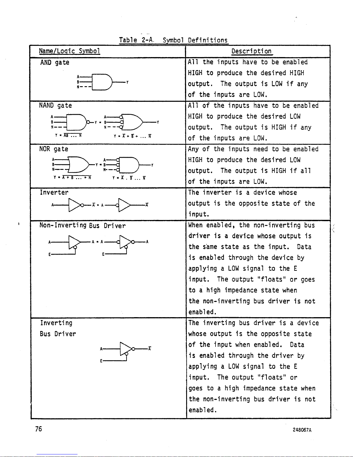
Table 2-A, Symbol Definitions
Name/Loqic Symbol
AND gate
NAND gat
e
8
Y
« Afl
••• d Y * 7T • F + ... IT
NOR gate
A X A d
B )—Y
« B
N—N- C
Y » A
• B ... • N
Y«
Inverter
A
^>0—A » A C -J
C
I
. F ...
w
Y
Descri
pti
on
All the inputs have to be enabled
HIGH to produce the desired HIGH
output. The output is LOW if any
of the inputs are LOW.
All of the inputs have to be enabled
HIGH to produce the desired LOW
output. The output is HIGH if any
of the inputs are LOW.
Any of the inputs need to be enabled
HIGH to produce the desired LOW
output. The output is HIGH if all
of the inputs are LOW.
The inverter is a device whose
output is the opposite state of the
input.
Non-Inverting Bus Driv*
sr
A A » A—C
Inverting
Bus Driver
A
£
When enabled, the non-inverting bus
driver is a device whose output is
the same state as the input. Data
is enabled through the device by
applying a LOW signal to the E
input. The output "floats11 or goes
to a high impedance state when
the non-inverting bus driver is not
enabled.
The inverting bus driver is a device
whose output is the opposite state
of the input when enabled. Data
is enabled through the driver by
applying a LOW signal to the E
input. The output "floats" or
goes to a high impedance state when
76
the non-inverting bus driver is not
enabled.
248067A
Page 87
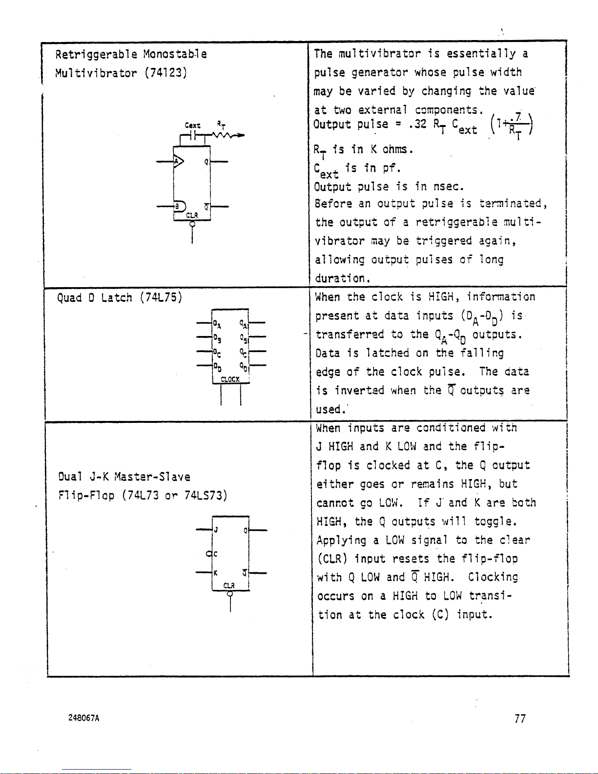
Retriggerable MonostaWe
Multivibrator (74123)
Cast
The multivibrator is essentially a
pulse generator whose pulse width
may be varied by changing the value'
at two external components.
Output pulse = .32 Rj C
gxt
Rj is in K ohms.
C
ext
is ™ pf
*
Output pulse is in nsec.
Before an output pulse is terminated,
the output of a retriggerable multivibrator may be triggered again,
allowing output pulses of long
duration.
Quad D Latch (74L75)
4
°C
*
°0
<4
accx :
u
When the clock is HIGH, information
present at data inputs (D^-O-j) istransferred to the outputs.
Oata is latched on the falling
edge of the clock pulse. The data
is inverted when the outputs are
used.'
Dual J-K Master-Slave
FT ip-Flop (74L73 or 74LS73)
When inputs are conditioned with
J HIGH and K LOW and the flipflop is clocked at C, the Q output
either goes or remains HIGH, but
cannot go LOW. If J' and K are both
HIGH, the Q outputs will toggle.
Applying a LOW signal to the clear
(CLR) input resets the flip-flop
with Q LOW and Q" HIGH. Clocking
occurs on a HIGH to LOW transi-
tion at the clock (C) input.
248067A
77
Page 88
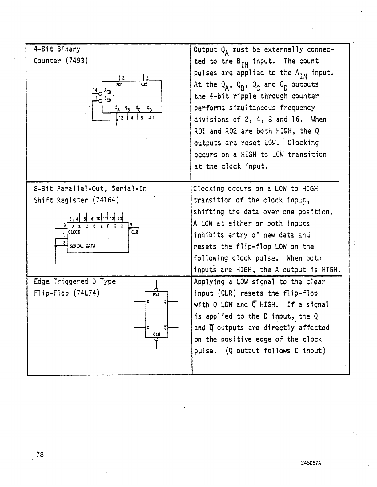
4-Bit Binary
Counter (7493)
Output Q^ must be externally connec-
ted to the input. The count
pulses are applied to the A^ input.
At the QA, QB, QC and Qq outputs
the 4-bit ripple through counter
performs simultaneous frequency
divisions of 2, 4, 8 and 16. When
ROl and R02 are both HIGH, the Q
outputs are reset LOW. Clocking
occurs on a HIGH to LOW transition
at the clock input.
8-Bit Parallel-Out, Serial-In
Shift Register (74164)
Clocking occurs on a LOW to HIGH
transition of the clock input,
shifting the data over one position.
A LOW at either or both inputs
inhibits entry of new data and
resets the flip-flop LOW on the
following clock pulse. When both
inputs are HIGH, the A output is HIGH,
Edge Triggered D Type
Flip-Flop (74L74)
Applying a LOW signal to the clear
input (CLR) resets the flip-flop
with Q LOW and $ HIGH. If a signal
is applied to the 0 input, the Q
and IT outputs are directly affected
on the positive edge.of the clock
pulse. (Q output follows D input)
78
248067A '
Page 89
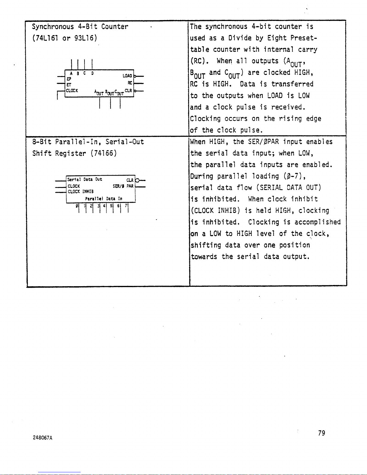
Synchronous 4-Bit Counter
The synchronous 4-bit counter is
(74L161 or 93L16)
8-Bit Parallel-In, Serial-Out
Shift Register (74166)
Serial Data Out
ri
ocx
CLOCK INHIB
Parallel
Data In
OR
SER/& PAR
SER/& PAR
31 It 21 3 4 5 61 7
used as a Divide by Eight Presettable counter with internal carry
(RC). When all outputs (AqUT,
B
and Cqjjj) are clocked HIGH,
qut
RC is HIGH. Data is transferred
to the outputs when LOAD is LOW
and a clock pulse is received.
Clocking occurs on the rising edge
of the clock pulse.
When HIGH, the SER/0PAR input enables
the serial data input; when LOW,
the parallel data inputs are enabled.
During parallel loading (2-7),
serial data flow (SERIAL DATA OUT)
is inhibited. When clock inhibit
(CLOCK INHIB) is held HIGH, clocking
is inhibited. Clocking is accomplished
on a LOW to HIGH level of the clock,
shifting data over one position
towards the serial data output.
248067A '
79
Page 90
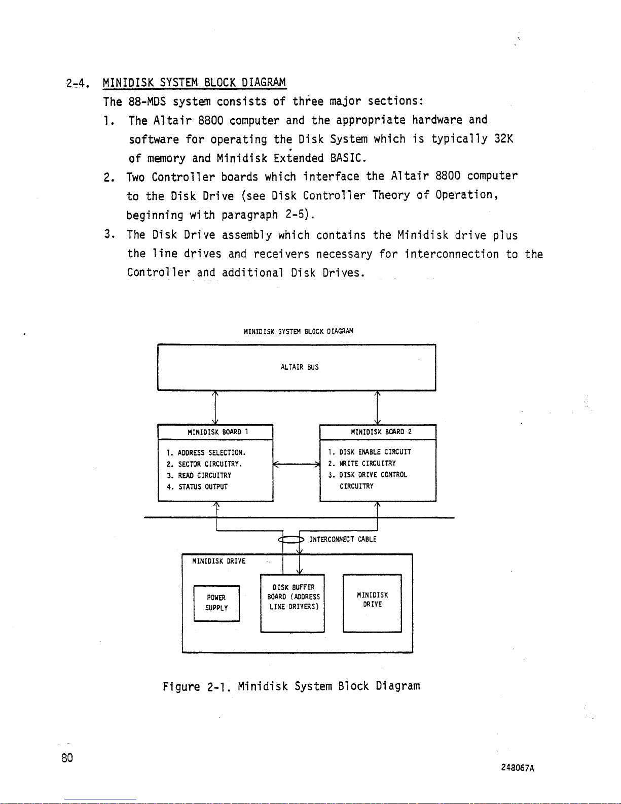
MINIDISK SYSTEM BLOCK DIAGRAM
The 88-MDS system consists of three major sections:
1. The Altair 8800 computer and the appropriate hardware and
software for operating the Disk System which is typically 32K
of memory and Minidisk Extended BASIC.
2. Two Controller boards which interface the Altair 8800 computer
to the Disk Drive (see Disk Controller Theory of Operation,
beginning with paragraph 2-5).
3. The Disk Drive assembly which contains the Minidisk drive plus
the line drives and receivers necessary for interconnection to the
Controller and additional Disk Drives.
MINIDISK SYSTEM BLOCK DIAGRAM
Figure 2-1. Minidisk System Block Diagram
243067A
Page 91
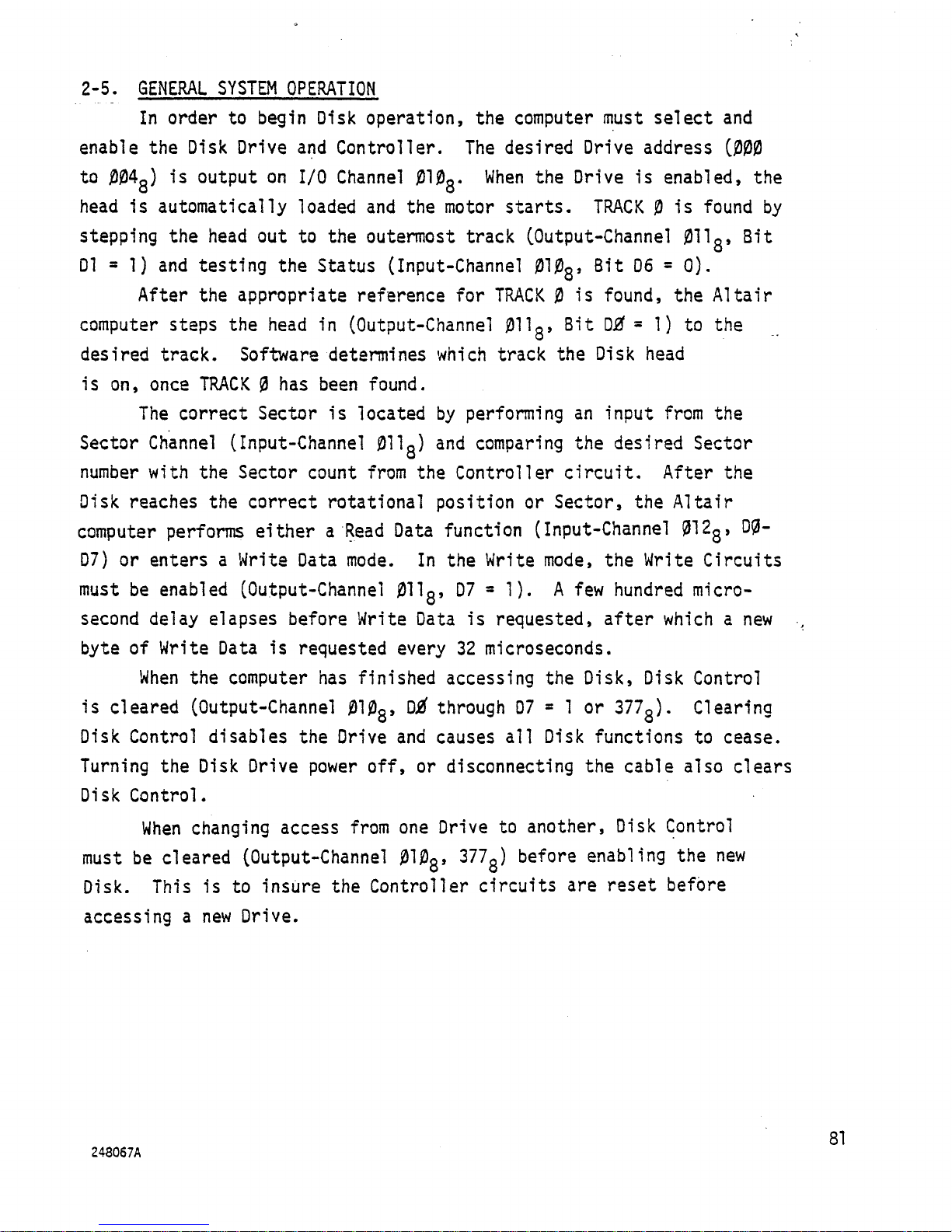
2-5. GENERAL SYSTEM OPERATION
In order to begin Disk operation, the computer must select and
enable the Disk Drive and Controller. The desired Drive address (000
to 004g) is output on I/O Channel 010g. When the Drive is enabled, the
head is automatically loaded and the motor starts. TRACK 0 is found by
stepping the head out to the outermost track (Output-Channel 011g> Bit
D1 • 1) and testing the Status (Input-Channel 010q, Bit D6 = 0).
After the appropriate reference for TRACK 0 is found, the Altair
computer steps the head in (Output-Channel 011g> Bit DJ3" = 1) to the
desired track. Software determines which track the Disk head
is on, once TRACK 0 has been found.
The correct Sector is located by performing an input from the
Sector Channel (Input-Channel 011q) and comparing the desired Sector
number with the Sector count from the Controller circuit. After the
Disk reaches the correct rotational position or Sector, the Altair
computer performs either a Read Data function (Input-Channel 012g, D0-
D7) or enters a Write Data mode. In the Write mode, the Write Circuits
must be enabled (Output-Channel 011g, D7 = 1). A few hundred micro-
second delay elapses before Write Data is requested, after which a new
byte of Write Data is requested every 32 microseconds.
When the computer has finished accessing the Disk, Disk Control
is cleared (Output-Channel 010g, DJti through D7 = 1 or 377g). Clearing
Disk Control disables the Drive and causes all Disk functions to cease.
Turning the Disk Drive power off, or disconnecting the cable also clears
Disk Control.
When changing access from one Drive to another, Disk Control
must be cleared (Output-Channel 010g, 377g) before enabling the new
Disk. This is to insure the Controller circuits are reset before
accessing a new Drive.
248067A '
81
Page 92
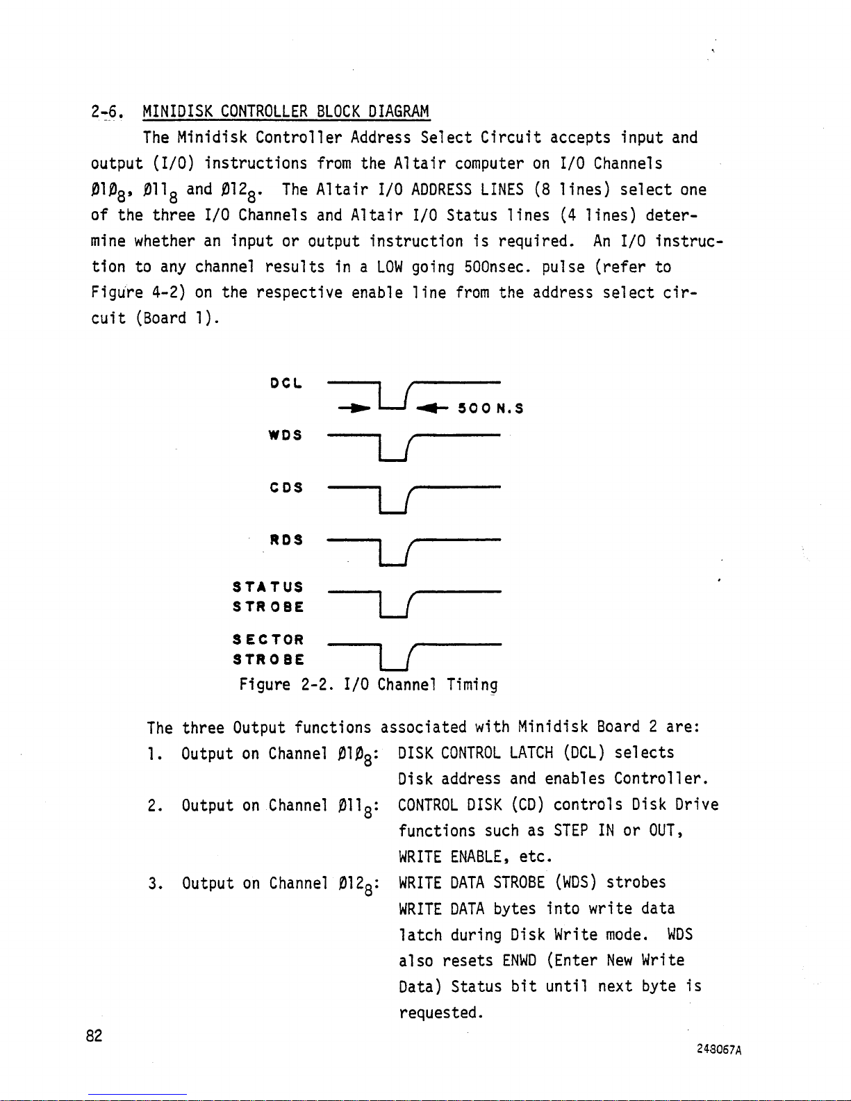
2-6. MINIDISK CONTROLLER BLOCK DIAGRAM
The Minidisk Controller Address Select Circuit accepts input and
output (I/O) instructions from the Altair computer on I/O Channels
0108, 0118 and 012g. The Altair I/O ADDRESS LINES (8 lines) select one
of the three I/O Channels and Altair I/O Status lines (4 lines) determine whether an input or output instruction is required. An I/O instruc-
tion to any channel results in a LOW going 500nsec. pulse (refer to
Figure 4-2) on the respective enable line from the address select circuit (Board 1).
OCL
u.
WOS
500 N.S
w
COS
w
ROS
w
STATUS
STR OBE
SECTOR
STROBE
Figure 2-2. I/O Channel Timing
The three Output functions associated with Minidisk Board 2 are:
1. Output on Channel 0108: DISK CONTROL LATCH (DCL) selects
2. Output on Channel 011g: CONTROL DISK (CD) controls Disk Drive
3. Output on Channel 0128: WRITE DATA STROBE (WDS) strobes
If
is
Disk address and enables Controller.
functions such as STEP IN or OUT,
WRITE ENABLE, etc.
WRITE DATA bytes into write data
latch during Disk Write mode. WDS
82
also resets ENWD (Enter New Write
Data) Status bit until next byte is
requested.
243067A
Page 93
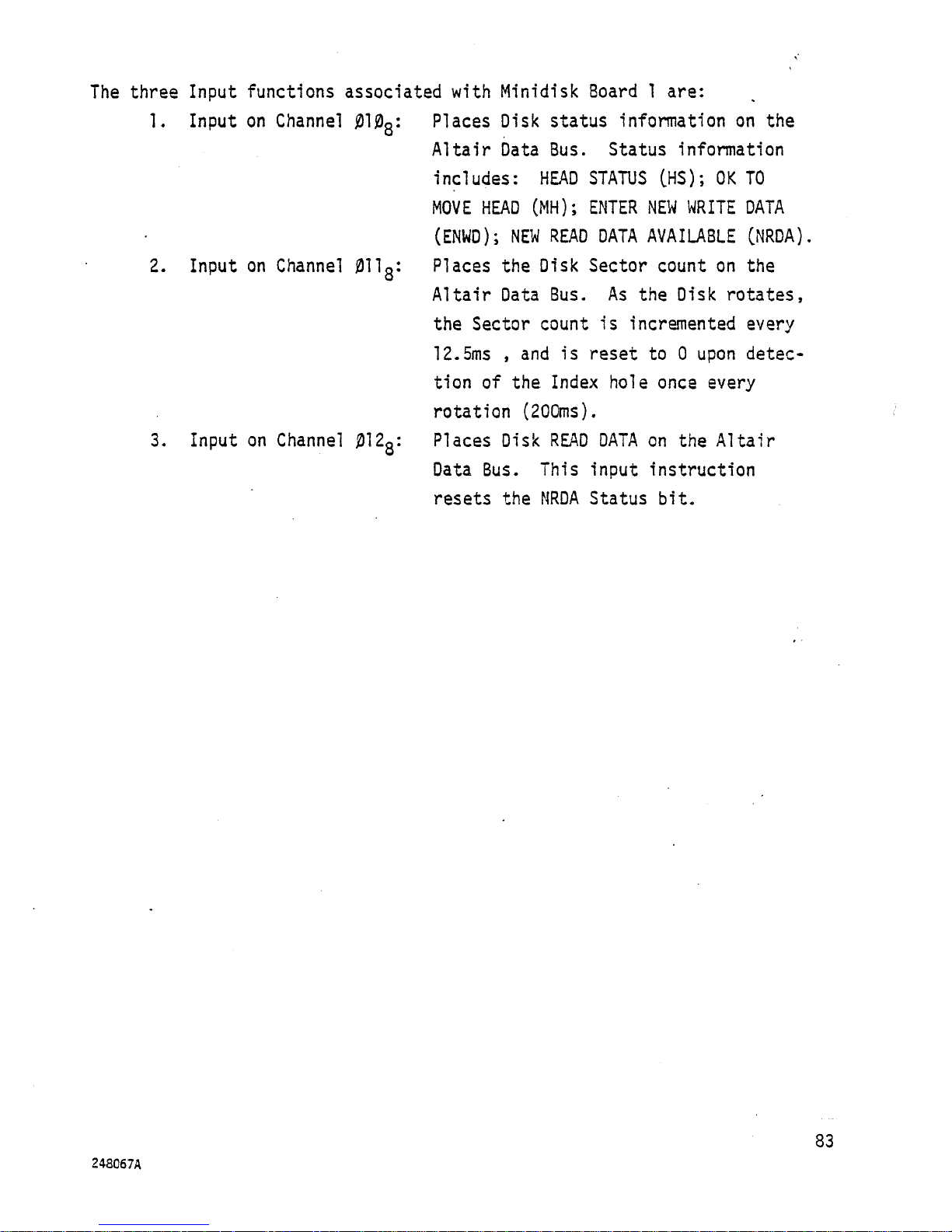
The three Input functions associated with Minidisk Board 1 are:
Input on Channel 010g:
2. Input on Channel 011g:
3. Input on Channel 012g:
Places Disk status information on the
Altair Data Bus. Status information
includes: HEAD STATUS CHS); OK TO
MOVE HEAD (MH); ENTER NEW WRITE DATA
(ENWD); NEW READ DATA AVAILABLE (NRDA).
Places the Disk Sector count on the
Altair Data Bus. As the Disk rotates,
the Sector count is incremented every
12.5ms , and is reset to 0 upon detection of the Index hole once every
rotation (200ms).
Places Disk READ DATA on the Altair
Data Bus. This input instruction
resets the NRDA Status bit.
248067A 93
Page 94
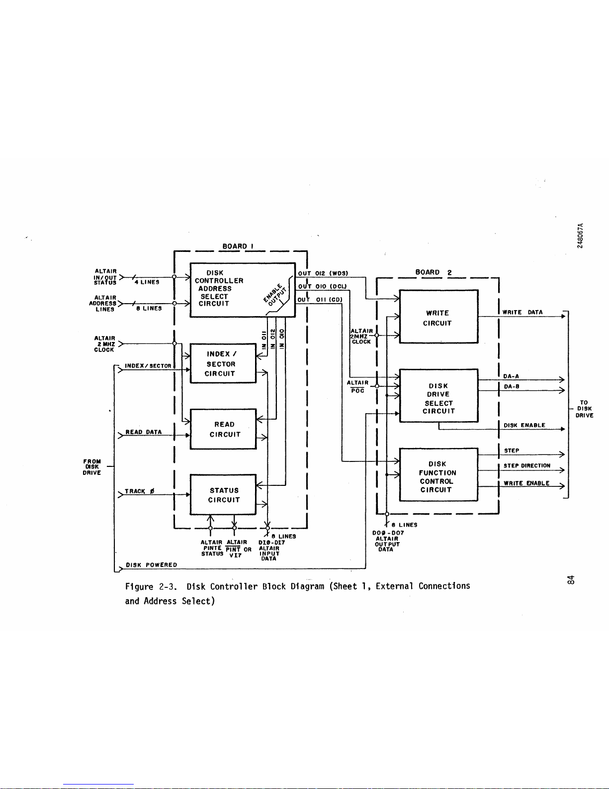
<
BOARD I ^
Figure 2-3. Disk Controller Block Diagram (Sheet 1, External Connections
and Address Select)
Page 95
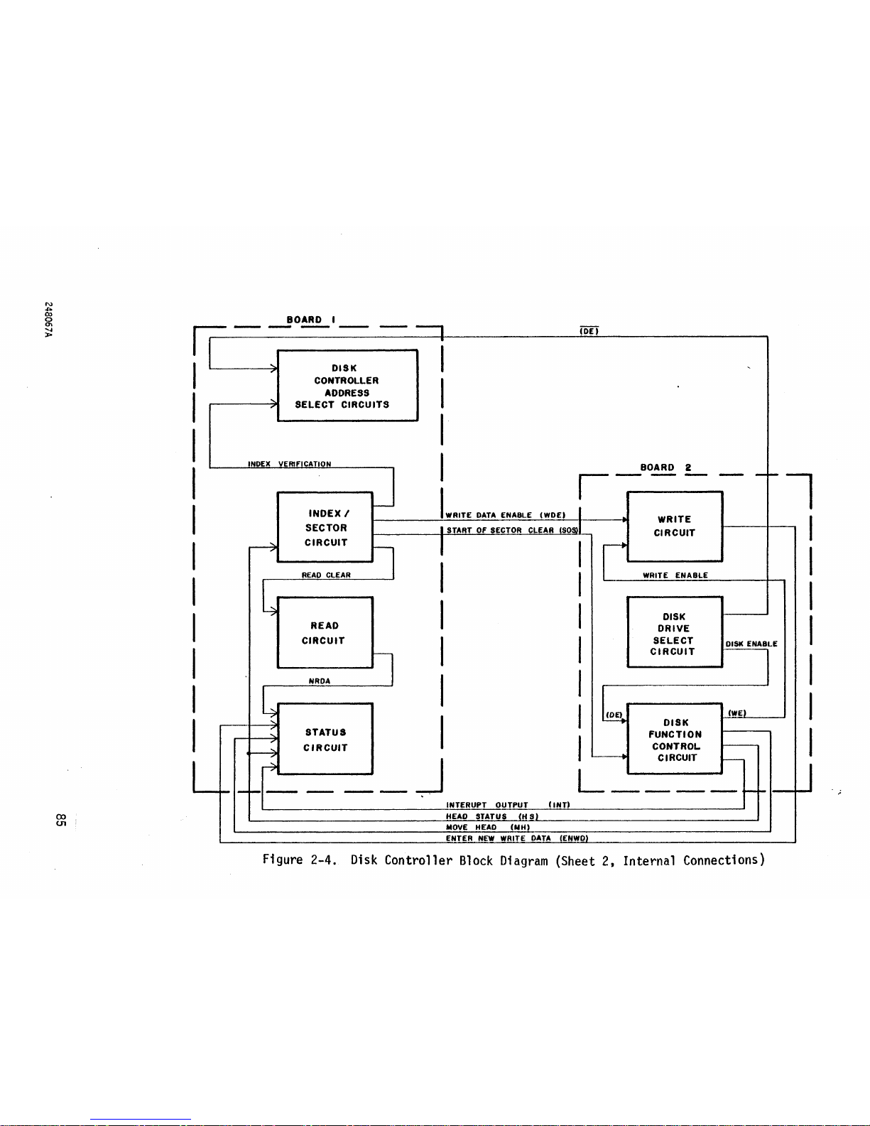
BOARD I
Figure 2-4. Disk Controller Block Diagram (Sheet 2, Internal Connections)
Page 96
Upon an Output to Channel 010g, the DISK CONTROL LATCH (DCL),
Disk Drive Select Circuits are enabled with DA-A and DA-B, selecting
one of four possible Minidisk Drives. The DISK POWERED line enables
the Disk Drive Select Circuit when the Drive selected is properly
connected and powered. When the Minidisk Drive is selected and enabled,
the DISK ENABLE (DE) signal is presented to the Disk Function Control
Circuit where DE enables the Status information.
The Disk Function Control Circuits, when selected, load the head
on the Disk (HEAD LOAD), step the head out (STEP OUT), step the head in
(STEP IN) and enable the Write Circuit (WRITE ENABLE). Control Circuits
also produce INTERRUPT OUTPUT, MOVE HEAD or HEAD STATUS signals which
are transferred to the Disk Status Circuits. Control signals, Disk
address information and WRITE DATA are transferred from the Altair
computer to Controller Board 2 by eight Output Data Lines (D0O-D07).
WRITE DATA is transferred to the Write Circuit upon an output to
Channel 012g, the WRITE DATA STROBE (WDS). The rate of serial WRITE
DATA to the Disk is controlled by dividing the Altair 2MHz Clock.
ENTER NEW WRITE DATA (ENWD) is the Status signal generated by the Write
Circuit when new WRITE OATA is requested.
When INDEX and SECTOR pulses are received by the Index/Sector
Circuit, the INDEX pulse is detected, Sector count (beginning with
Sector &) may begin. The Index/Sector Circuit is synchronized by the
Altair 2MHz Clock, and upon an Output to Channel 011g, the Sector count
is presented. The Index/Sector Circuit also provides a START OF SECTOR
CLEAR (SOS) signal to the Disk Function Control Circuit, a WRITE DATA
ENABLE (WDE) signal to the Write Circuit and the READ CLEAR signal to
the Read Circuit. INDEX VERIFICATION and a True (LOW) condition on
HEAD STATUS must be present before the Address Select Circuits can
enable the Sector information from Channel 011
g..
When READ DATA is present from the Disk Drive and transferred to
the Altair Data Bus, the Read Circuit is enabled by addressing Input
Channel 012g. The Read Circuit provides the NRDA (NEW READ DATA
AVAILABLE) Status signal when READ DATA is detected.
86 248067A
Page 97
The Status Circuit provides information on the state of the
Controller and Disk Drive. A desired track is found by referencing
TRACK 0 (the outermost track). TRACK 0, NRDA and the other Status
signals are enabled by addressing Input Channel 010g. Input data is
transferred from the Index/Sector Circuit, Read Circuit or Status Circuit to the Altair computer by eight Input Data Lines (DI0-DI7).
2-7. ADDRESS SELECT CIRCUIT
The Address Control Circuit (Figure 2-14, Sheet 1) accepts I/O
instructions from the Altair computer on Channels 0108, 0118 and 012g.
To enable any of the strobe gates A3, A4 or A5, F5 pin 8 (zone
D7) must be enabled LOW. F5 pin 8 is LOW when address lines A15-A8
(zones C8 and D8) equal 01Xg. (X represents a User Selectable condi-
tion for A8-A10). A15-A12 is LOW, inverted HIGH at G5 pins 2, 4, 6 and
8 (zone D8) and appear HIGH at F5. With All HIGH, F5 pin 8 goes LOW
and is inverted HIGH to A5 pin 1 (zone D6). Address lines A10-A8,
when equal to XX0g, XXI8 or XX2g (XX represents a User Selectable con-
dition for address lines A11-A15 described above), enable one of the
AND gates B4 pins 6, 8 or 12 (zone C6). When A8, A9 and A10 are all
LOW, B4 pin 6 is enabled, allowing an Input or Output on Channel 010g.
When A9 is HIGH and A10 and A8 are LOW, B4 pin 12 is enabled, allowing
an Input or Output on Channel 012g. When A8 is HIGH and A10 and A9 are
LOW, B4 pin 8 is enabled, allowing an Input or Output on Channel 011g.
AND gates B4 determine the I/O Channel to be addressed since only one
gate is enabled at a time. A specific output instruction is then
selected if SOUT is HIGH and PWR is LOW (zone D8), and the specific
input instruction is recognized when SINP and PDBIN are HIGH (zone D8).
When the Disk is enabled, the Disk Enable line (DE, zone D8) goes HIGH,
enabling the INPUT STATUS STROBE (Channel 0108) and allowing the Index
Verification Flip-Flop, B3 (zone C3) to be clocked.
248067A '
87
Page 98
2-8. INDEX/SECTOR CIRCUIT (J311g - Input)
As the Minidiskette rotates in the Drive, an optoelectronic sensor
detects the 16 Sector holes and the Index hole on the Diskette. The
Sector holes generate a 4.4ms pulse every 12.5ms.. (Refer to Figure
4-5 for timing diagram relating to Index/Sector Circuits). The Index
hole, located halfway between Sector holes 15 and 0, generates a 4.4ms
pulse every revolution (200.0ms.).
The Index or Sector pulse (IND) appears LOW and is inverted HIGH
to E5 pin 2 (Figure 4-14, Sheet 1, zone C6). E5 pin 3 is enabled LOW
until E3 pin 13 (zone C5) is clocked. The 2MHz Clock (zone B8) goes
LOW at pin 49 of the bus and is inverted by J3 pin 8, clocking the
Sector Pulse Compressor Flip-Flop, E3 pin 13 (zone Co). The output
pulse width (500ns £ 250ns ) of E5 pin 3 (zone C6) is dependent on
the propagation time of the flip-flop and the delay time of the RC time
constant of R7 and C30. After being inverted, E5 pin 3 appears HIGH
at the Index Window Gate, A4 pin 11 (zone C5). A4 separates the Index
pulse from the Sector pulses. A2 pin 10 is enabled HIGH when E5 pin 3
goes LOW. Sector Pulse One Shot, El pin 13 (zone C4), goes HIGH for
3G0ys which triggers Index Window One Shot, El pin 5 (zone C4), HIGH
for 9.6ms. A4 pin 8 (zone C5) is only enabled when the Index pulse
enables E5 pin 3 since El pin 4 (zone C4) and El pin 5 are HIGH at A4
pins 9 and 10 during this time. The 300us LOW going pulse at El pin 4
also toggles the 4 Bit Sector Counter, G4 pin 14 (zone A3).
El pin 5 is HIGH, leaving A2 pin 8 (zone C5) HIGH when the Index
pulse appears at A2 pin 9. As a result, A2 pin 10 is not enabled when
the Index pulse appears, allowing only Sector pulses to trigger El pin
13 (zone C4). In addition to enabling El at pin 10 (zone C4), the HIGH
300us pulse at El pin 13 is also present at E2 pin 10 (zone B6). E2
pin 8 is enabled LOW when El pin 13 is HIGH, since E3 pin 8 (zone B6)
is in a reset condition (E3 pin 8 HIGH). The 2MHz Clock enables the
Sector Pulse One Shot Compressor, F2 pin 9 (zone B7) HIGH, and on the
88
248067A '
Page 99
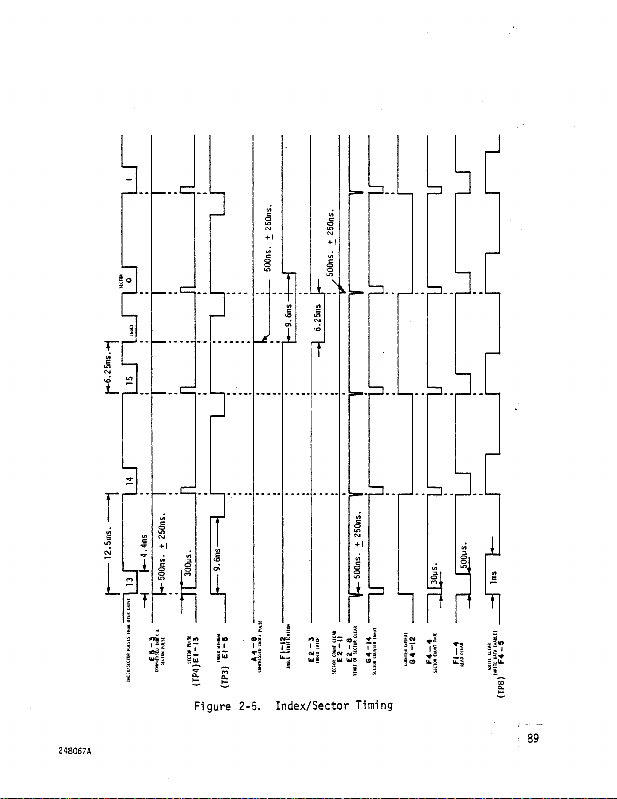
T"
-JsLJl
c
o
U)
CVJ
+1
c
o
o
W)
Ll
o
in
CVJ
+1
c
o
o
uo
c
o
CO
CM
c
o
o
to
,.LL\
CVJ
rr
I
I:
10
i
I
|UJ
CO
o.
i
1
r§
Ts
i
i
J
.-zn..
ut
c
o
cr>
CVJ
+ 1
</)
c
o
o
LO
o
o
Jj
11
1
<
CM 5
uii
5 « I _
§M CVJ-
«UI UiS
U.S
Ti
=1
5 =
CO
Q.
Figure 2-5. Index/Sector Timing
248067A
: 89
Page 100
falling edge enables E3 pin 8 LOW. When E3 pin 8 goes LOW, E2 pin 8
is disabled. When E2 pin 8 is disabled HIGH, the Sector Count True
One Shot, F4 pin 4 (zone A7), toggles LOW for 30ys. If it is the first
Sector pulse after the Index pulse,.the Index Latch, E2 pins 3 and 6
(zone A5) is reset, forcing E2 pin 3 HIGH. The LOW at E2 pin 8 also
appears on board 2 (Figure 2-15, Sheet 1, zone A8) as the START OF
SECTOR CLEAR (SOS) signal, which clears the Write Circuit at the end
of a Write mode.
After a valid Index pulse has been detected, A4 pin 8 (Figure
2-14, Sheet 1, zone B5) is enabled LOW, setting the Index Latch with
E2 pin 3 LOW. When E2 pin 3 is LOW, the Index Latch Pulse Compressor,
F3 pin 13 (zone B5), is cleared. A4 pin 8 also triggers F1 pin 12
(zone B3) LOW for 9.6ms. After 6.25ms , the Index Latch is reset by a
Sector pulse, leaving E2 pin 3 HIGH. E2 pin 11 (zone B5) is enabled LOW
until the Index Latch Pulse Compressor Flip-Flop, F3 pin 13, is
clocked by the 2MHz Clock pulse. The 500ns. (+250ns ) output pulse at
E2 pin 11 is dependent on the propagation time of F3 pin 13 and the
delay time of the RC time constant of R8 and C20. A2 pin 1 (zone C3)
is HIGH for 500ns (+250ns ) if FT pin 12 (zone B3) has been triggered LOW. This clocks B3 pin 8 (zone C3) LOW if B3 pin 7, the HEAD STATUS
(HS) signal, is HIGH. HEAD STATUS should go HIGH 50ms. after the head
is loaded on the Disk. A LOW at B3 pin 8 indicates that the correct
Index pulse has been detected. The Index Latch, in allowing E2 pin 11
to be enabled, also resets the 4 Bit Sector Counter, G4, at pins 2 and
3 (zone A3), and the 5th Bit Sector Count Flip-Flop, F3 pin 6 (zone B4).
Since this occurs on the first Sector pulse after the Index pulse, a
correct Sector count is guaranteed every revolution. INPUT SECTOR
STROBE (Channel 011g) is enabled when A2 pin 4 (zone C2) goes HIGH.
This occurs only when the Index Verification Flip-Flop is set (B3 pin
8 LOW) and the HEAD STATUS signal is LOW, indicating that the head is
properly loaded for reading and writing. Drivers H5 pins 9, 11, 5, 7, .
3 and 13 (zone B2) are then enabled when A3 pin 8 (zone B3) goes LOW.
The Sector count is then transferred to the bus. The correct Sector
is located by comparing the desired Sector number with the Sector
count from this Index/Sector Circuit. Software also checks DIO to see
gif it is the beginning of the Sector.
248067A 100
 Loading...