MITEL WL800TP1R, WL800KG, WL800 Datasheet

FEATURES
■ Low power consumption
■ 2.5GHz input
■ 144 frequencies, 1MHz steps (20MHz crystal)
■ Forms complete phase locked loop using external
VCO and loop components
■ Serially programmed via 3 wire bus
■ Contains anti-modulation circuit
■ Part of DE6038 Chip-set (WL600C, WL102)
ORDERING INFORMATION
WL800/KG/TP1R
The WL800 is a low power single chip frequency synthesiser.
The circuit is fabricated on Mitel Semiconductor HG process
and operates from a supply voltage of 2.7 - 3.6V. It is designed
to work with the Mitel Semiconductor WL600C RF and IF
circuit and the WL102 WLAN controller chip which together
make up the DE6038 frequency hopping Wireless Local Area
Network (WLAN) transceiver.
RELATED DOCUMENTS
WL600C, WL102 datasheets
TQFP 32
Fig.1 Pin connections - top view
PIN 1 IDENT
ABSOLUTE MAXIMUM RATINGS
Supply Voltage Vcc 4VDC
Transmit/Receive and -0.5VDC to Vcc +0.5VDC
Standby Input
Prescaler Inputs Pins 30 &31 No DC. Externally Capacitively
Coupled.
Output Current (any output) TBD mA
Junction temperature Tj 150°C
ESD protection: 2kV
Operating temperature -20 to +85°C
WL800
2.5GHz Frequency Synthesiser
Preliminary Information
DS4583 1.6 October1997

2
WL800
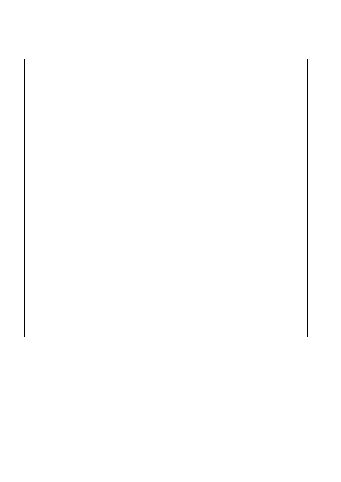
PIN REFERENCE TYPE DESCRIPTION
1 VCC1 VCC Power for serial data bus
2 CS-DATA IN Channel Data in (Synth Programming)
3 CS-CLK IN Data Clock (Synth Programming)
4 CS-LOADB IN Data Enable (Synth Programming)
5 STDBYB IN Power down control Active = Logic 1 Standby = logic 0
6 VEE1 GND Ground connection
7 ISET Set modulation current
8 ICP Set charge pump current
9 VEE3 GND Ground connection
10 TXD IN Modulation data in
11 COM CAP Compensation capacitor for modulation data
12 RCOMP OUT Resistor for V/I converter
13 IDOUT OUT Modulation data out
14 TXRXB IN Transmit/Receive control Transmit = Logic 1 Receive = Logic 0
15 VARICAP OUT Control V to varicap in VCO
16 VCC3 VCC Power for charge pump and loop amplifier and modulator
17 LOOPFILTER OUT Loop filter out (Loop Filter Components)
18 CPUMPREF Charge pump reference voltage
19 CPUMPOUT OUT Charge pump out (Loop Filter Components)
20 VEE2 GND Ground connection
21 SYSCLK OUT Reference (system) clock out
22 XTAL Crystal connection (Differential)
23 XTALB Crystal connection (Differential)
24 VCC2 VCC Power for reference oscillator
25 FREF OUT Reference frequency monitor
26 LKCAP Lock detect capacitor
27 LCKDETB OUT Lock detect output
28 FV OUT VCO frequency / (NM+A) monitor
29 VEE5 GND Ground connection
30 VCC VCC Power for prescaler, AM counter Ref divider, phase detector and
lock detector
31 VCOIPB IN Prescaler IN32 VCOIP IN Prescaler IN+
DEVICE PIN OUT

3
WL800
PRE-SCALER A COUNTER
PHASE DET
& CHARGE
PUMP
INPUT REGISTER
M COUNTER
REFERENCE
OSC
DIVIDE
BY 20
REF OUT
BUFFER
LOCK
DETECT
PRE
AMP
DATA
BUFFER
1,16,24,30
Vcc
6,9,20,29
Vee
STANDBY
5
14
TXRXB
DATA
2
CLK
3
ENABLEB
4
VCOIP
32
VCOIPB
31
DIN
10
IDOUT
13
ISET
7
21
REF
OUT
23
XTAL122XTAL2
LKCAP
26
LKDETB
27
CPUMP
REF
18
VARICAP
15
LOOP
FILTER
17
CPUMP
OUT
19
MOD
COMP
COMP
11
ICP
8
FREF
25
28
FV
12
RCOMP
VCAP
CHARGE
CAP
BUFFER
1/3
SYSCLK
STDBYB
LCKDETB
COMPCAP
TXD
CS-DATA CS-CLK
CS-LOADB
B
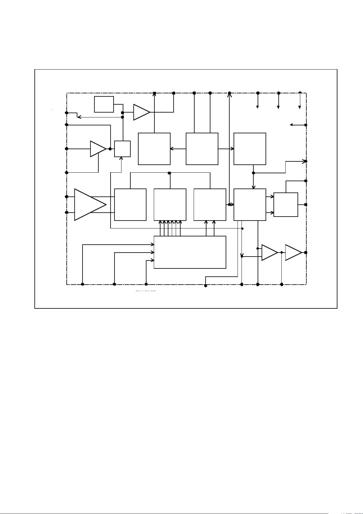
Fig. 1 WL800 block diagram
XTALB

4
WL800
ELECTRICAL CHARACTERISTICS
These characteristics are guaranteed over the following conditions (unless otherwise stated):
T
AMB
= -20°C, to +85°C, Vcc = 2.7V to 3.6V
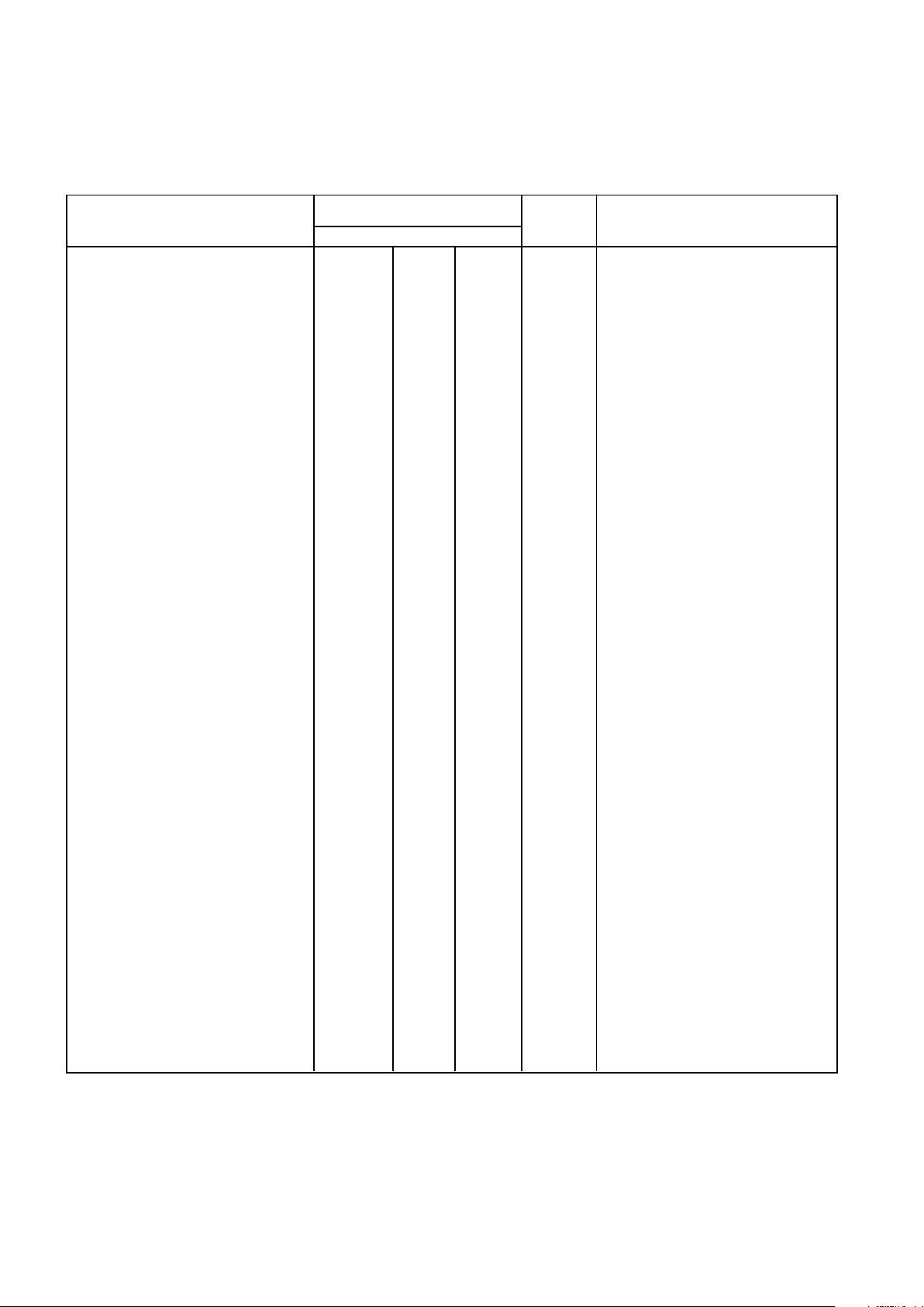
Characteristic Value Unit Condition
MIN TYP MAX
Supply current (total)
Transmit 37 50 mA
Receive 35 50 mA
Supply current in standby 3 5 mA
PROGRAMMING INPUTS
Logic low voltage 0 0.4 V
Logic high voltage 0.8Vcc Vcc V
Input current 1 µA Input level high
Data clock frequency (1/tclock) 20 MHz See Fig. 2
Data/Enable set up time (t set up) 10 ns See Fig. 2
Enable hold time (t enable) 10 ns See Fig. 2
Positive clock pulse width (tp) 20 ns See Fig. 2
Negative clock pulse width (t neg) 20 ns See Fig. 2
STANDBY INPUT
Logic low input voltage 0 0.8 V Circuit powered down
Logic high input voltage Vcc -0.7 Vcc V Circuit powered up
Input current 100 150 µA Circuit powered up
-150 µA Circuit powered down
Standby to operate time 3 µs *References operational (see note 1)
TX/RX INPUT
Logic low input voltage 0 0.8 V Receive mode
Logic high input voltage Vcc -0.7 Vcc V Transmit mode
Input current 10 µA
REFERENCE OUTPUT
Reference output frequency 20 MHz With 20MHz crystal
Reference clock output voltage 200 250 300 mVp-p With 15pF load
Reference output impedance 600 Ohms
Mark Space ratio -2% 50/50 +2% With 15pF load
Rise time 15 ns
Fall time 15 ns
Crystal Drive Levels required 200 mV Pins 22,23 differential
 Loading...