SP8858
1·5GHz Professional Synthesiser
Supersedes March 1997 version, DS3843 - 3.0 DS3843 - 4.1 July 1998
The SP8858 is a single chip synthesiser intended for PLL
signal synthesis applications up to 1.5GHz and includes a
dual modulus prescaler (4N/N11), programmable A, M and
R dividers, digital phase detector, charge pump and lock
detect circuits.
The SP8858 is a development of the SP8853 synthesiser
with low residual phase noise, increased dynamic range
above 1GHz and an improved high gain phase detector
design that eliminates the dead-band.
The low prescaler modulus, programmable to either 16/17
or 8/9, together with the 15-bit M counter and 13-bit reference
counter make this device ideal for a diverse range of high
performance applications.
The nominal phase detector gain is set by a reference
current into pin 24 and the gain can be varied over a 4:1 range
when the device is programmed. The dividers, the phase
detector sense, the prescaler modulus and the data buffer
control logic are also programmable using the three wire
serial interface. An alternative 22-bit control word for the A
and M dividers and phase detector gain can be stored so
allowing fast frequency hopping and bandwidth switching by
simply toggling the logic level on pin 13 (F1/F2). In addition,
the A counter of the ‘active’ buffer can be programmed with
only 6 bits, allowing fast hopping to adjacent channels.
A simple exclusive - or lock detect circuit is also provided,
the sensitivity of which is determined by an external capacitor.
FEATURES
■ Low Residual Phase Noise (see Reference 1)
■ Operation to 1·5GHz over Full Temperature Range
■ High Input Sensitivity
■ Improved Linear Digital Phase Detector
■ Programmable Charge Pump Current: 10µA to 2 mA
■ On-chip 416/17 or 48/9 Dual Modulus Prescaler
■ Three-wire Serial Data Interface
■ 13-bit Reference Counter
■ 15-bit M Counter
■ Stores an Alternative Programming Word
■ Facility to Program A counter Only
■ Power Saving Standby Mode
F
REF
POWER DOWN
4
V
EE
4
V
CC
1
V
CC
RF INPUT
RF INPUT
F
REF
POWER DOWN
4
V
EE
4
V
CC
1
V
CC
RF INPUT
RF INPUT
4321282726
5
*
6
7
8
9
10
11
12 13 14 15 16 17 18
5
*
6
7
8
9
10
11
12 13 14 15 16 17 18
3
*
EE
PD
NC
V
F
1
EE
V
*
PD
F
4321282726
NCCDLOCK DETECT
SP8858
F1/F2
DATA
CLOCK
ENABLE
3
EE
NC
V
NCCDLOCK DETECT
NC
CP REF
25
24
23
22
21
20
19
2
CC
V
CP REF
SP8858
1
EE
V
F1/F2
DATA
CLOCK
NC
ENABLE
2
CC
V
25
24
23
22
21
20
19
CP OUTPUT
RPD
3
V
CC
GROUND
XTAL 1
XTAL2
2
V
EE
HC28
CP OUTPUT
RPD
3
V
CC
GROUND
XTAL 1
XTAL2
2
V
EE
HP28
ABSOLUTE MAXIMUM RATINGS
Supply voltage
Storage temperature
Operating temperature
Prescaler input voltage
20·3V to 17V
265°C to 1150°C
255°C to 1125°C
2·5V p-p
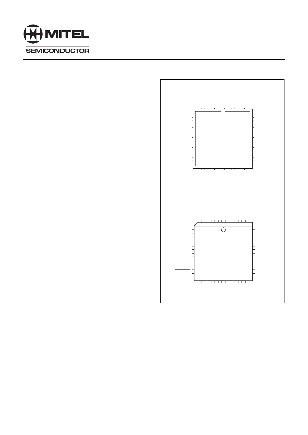
Fig. 1 Pin connections (top view)
ORDERING INFORMATION
SP8858 IG HCAR 240°C to 185°C (Industrial grade)
SP8858 MG HCAR 255°C to 1125°C (Military grade)
SP8858 IG HPAS 240°C to 185°C (Industrial grade)

SP8858
Pin Description
F
4
= M divider output pulses = RF input frequency 4(MN1A) when SENSE bit in the programming
PD
word = ‘0’. When SENSE bit = 1, this pin is F
= R divider output pulses = reference input
REF
frequency 4R. (see Data Entry and Control description and Fig. 6).
F
5
= R divider output pulses when SENSE bit in the programming word = ‘0’. When SENSE
REF
bit = 1, this pin is FPD = M divider output pulses (see Data Entry and Control description and
Fig. 6).
6 (POWER DOWN)
10, 11 (RF INPUT)
13 (F1/F2)
14 (DATA)
15 (CLOCK)
16 (ENABLE)
20 (XTAL 2)
21 (XTAL 1)
24 (RPD)
25 (CP OUTPUT)
With this pin held high the device is in the power saving standby mode. The serial interface shift
register and data buffers remain active at all times so that the device can still be programmed in
this mode.
Balanced inputs to the RF preamplifier. For single ended operation the signal is AC coupled into
pin 11 with pin 10 decoupled to ground or vice-versa.
The logic level on this input determines which of the two words stored in the internal buffers is used
to reload the A and M dividers at the end of the count cycle. With F1/F2 high the F1 buffer is selected.
Serial data on this line is clocked into a shift register under control of CLOCK and ENABLE.
Clocks the data into the shift register.
Logic high on this pin allows data to be clocked into the shift register and the subsequent falling edge
loads the buffer chosen by the LSBs of the programmed word. The clock input is ignored when
ENABLE is low.
This pin is the input to a buffer amplifier if an external reference signal is provided. Alternatively,
the amplifier provides the active element for a reference oscillator if a quartz crystal is connected
at this point (see Applications).
Leave open circuit if an external reference is used or connect load capacitors for the chosen crystal
(see Applications)
An external resistor connected between this pin and V
sets the charge pump output current. A
CC
multiplication factor can also be programmed into the device (see Table 3)
The phase detector output is a single-ended charge pump sourcing or sinking current to the
inverting input of an external loop filter.
26 (CP REF)
27 (LOCK DETECT)
28 (CD)
9 (V
1), 12 (VEE1)
CC
18 (V
2), 19 (VEE2)
CC
23 (VCC3), 2 (VEE3)
8 (V
4), 7 (VEE4)
CC
2
Connected to the non-inverting input of the loop filter to set the DC bias.
A current sink into this pin is enabled when the lock detect circuit indicates lock. Used to give
external indication of phase lock.
A capacitor connected to this point determines the lock detect integrator time constant and can be
used to vary the sensitivity of the phase lock indicator.
Pre-amp and prescaler supply.
Oscillator supply.
Charge pump supply.
ECL supply.
Table 1 Pin descriptions
MODULUS CONTROL
SP8858
RF INPUT
RF INPUT
F1/F2
DATA
CLOCK
ENABLE
POWER
DOWN
10
11
13
14
15
INTERFACE
16
6
16/17 OR 8/9
DATA
V
REF
20
CRYSTAL
COUNTER
XFV
3 BITS SELECT F1/F2
SELECT MODULUS
SELECT R
XFR
ACTIVE A
C1 C2
LSB MSB
DIVIDER
*
F
REF
sense bit in the F1/F2 programming word. The pin allocations
shown are correct when the sense bit is low (see Fig. 6).
21
f
4 BITS
PD
PD GAIN
2 BITS
PD1 PD2
DECODE
FV
XFV
FR
XFR
PHASE
DETECTOR
BUFFER
DISABLE
FV
A
COUNTER
22 BITS
16 BITS
FR
M
RESET
15 BITS
F1/F2 22-BIT DATA BUFFER
24-BIT SHIFT REGISTER
16-BIT REFERENCE BUFFER
13 BITS
R
and FPD outputs are reversed by the phase detector
LOCK
DETECT
PD
SENSE
CHARGE
PUMP
28
CD
27
LOCK
DETECT
24
RPD
25
CP OUTPUT
25
CP REF
4
FPD*
5
F
REF
*
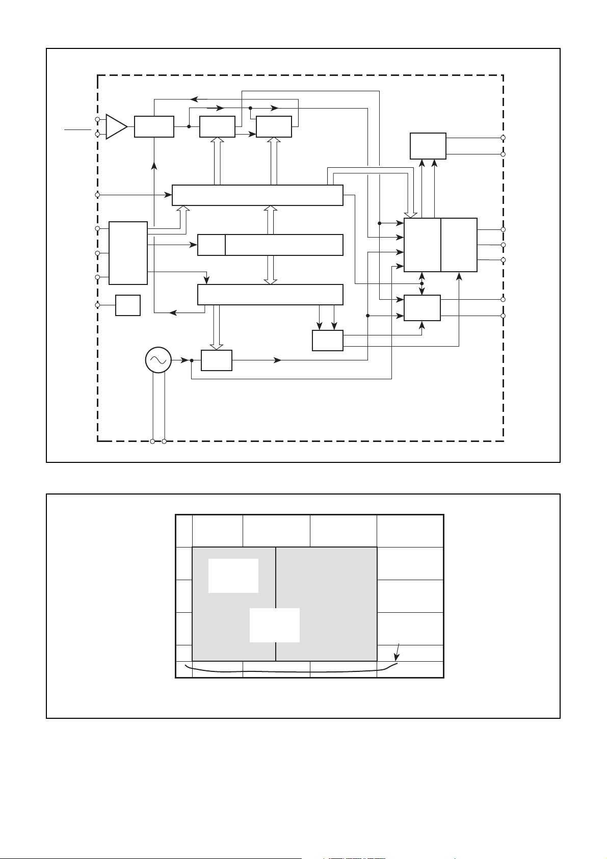
Fig. 2 SP8858 block diagram
500
400
GUARANTEED
300
200
INPUT VOLTAGE (mV RMS)
100
50
0
0
OPERATING
WINDOW
4
8/9 MODE
500
GUARANTEED
OPERATING
WINDOW
4
16/17 MODE
750
1000 150080
FREQUENCY (MHz)
Fig. 3 Typical input characteristics and input drive requirements
TYPICAL
SENSITIVITY
3

SP8858
ELECTRICAL CHARACTERISTICS
These characteristics are guaranteed over the following range of operating conditions unless otherwise stated:
Supply voltage VCC = 14·75V to 15·25V. T
= 255°C to 1125°C (Military), 240°C to 185°C (Industrial)
AMB
Characteristic Conditions
Supply current
Supply current in power down mode
Input sensitivity
Input overload
RF input division ratio
Comparison frequency
Reference oscillator input frequency
External reference input voltage
Reference division ratio
Data clock repetition rate, t
Minimum setup time, t
REP
S
DATA input high
DATA input low
CLOCK input high
CLOCK input low
ENABLE high
ENABLE low
F1/F2 input high
F1/F2 input low
POWER DOWN input high
POWER DOWN input low
F1/F2 input current
POWER DOWN input current
Current into RPD
Charge pump current
Charge pump current accuracy
Charge pump leakage
LOCK DETECT output voltage when in lock
F
and F
PD
output voltage swing
REF
Pin
8,9,18,23
8
10,11
10,11
10,11,4
4,5
20,21
20
20,5
15
14,15
14
14
15
15
16
16
13
13
6
6
13
6
24
25
25
25
27
27
Min.
400
240
56
50
50
0·6V
V
0·6V
V
0·6V
V
0·6V
V
0·6V
V
50
4
1
CC
EE
CC
EE
CC
EE
CC
EE
CC
EE
Value
Typ. Max.
95
35
110
45
50
524287
262143
5
40
600
8191
200
V
CC
0·3V
V
CC
0·3V
V
CC
0·3V
V
CC
0·3V
0·9V
0·3V
5
5
500
2
65
2
5
1
0·9
CC
CC
CC
CC
CC
CC
Units
mA
mA
mVrms
mVrms
MHz
MHz
mVrms
ns
ns
V
V
V
V
V
V
V
V
V
V
µA
µA
µA
mA
%
µA
V
See Fig. 3
See Fig. 3
With 416/17 selected
With 48/9 selected
See note 1
See Fig. 4
See Fig. 4
F1 buffer selected
F2 buffer selected
V pin 13 = 5·0V
V pin 6 = 4·5V
500µA34
Charge pump current = 2mA
I pin 27 < 3mA
= 5V, external pulldown
V
CC
may be required
LOCK DETECT output resistor
NOTE 1. The reference frequency range when using a crystal oscillator is 4-20MHz.
27
50
4
kΩ
tS1t
SP8858
CH
DATA
CLOCK
ENABLE
t
t
S-EN
2V
S
2V
t
CH
t
REP
t
S
t
CH
t
CL
t
E
t
S-EN
t
CL
t
REP
= tCH 1 tCL MIN
= 50ns MIN
= 100ns MIN
= 100ns MIN
= 50ns MIN
= [(31M)N1A]4RF INPUT (Hz)150ns
OR 14REFERENCE (Hz)150ns
WHICHEVER IS APPROPRIATE
(SEE DATA ENTRY AND CONTROL)
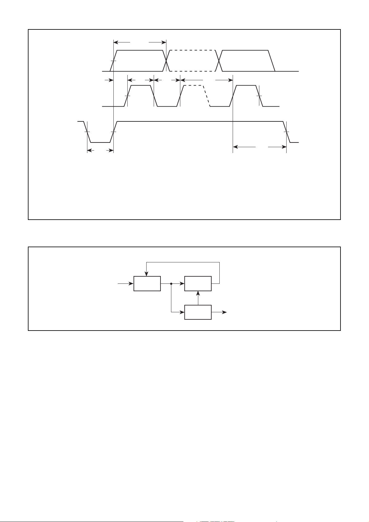
Fig. 4 DATA, CLOCK and ENABLE timing requirements
LAST DATA BITFIRST DATA BIT
2V
t
E
RF INPUT
PRESCALER
4
N / N11
MODULUS CONTROL
A
COUNTER
RESET
M
COUNTER
Fig. 5
RF INPUT 4(MN1A)
5
SP8858
DESCRIPTION
Prescaler and Dividers
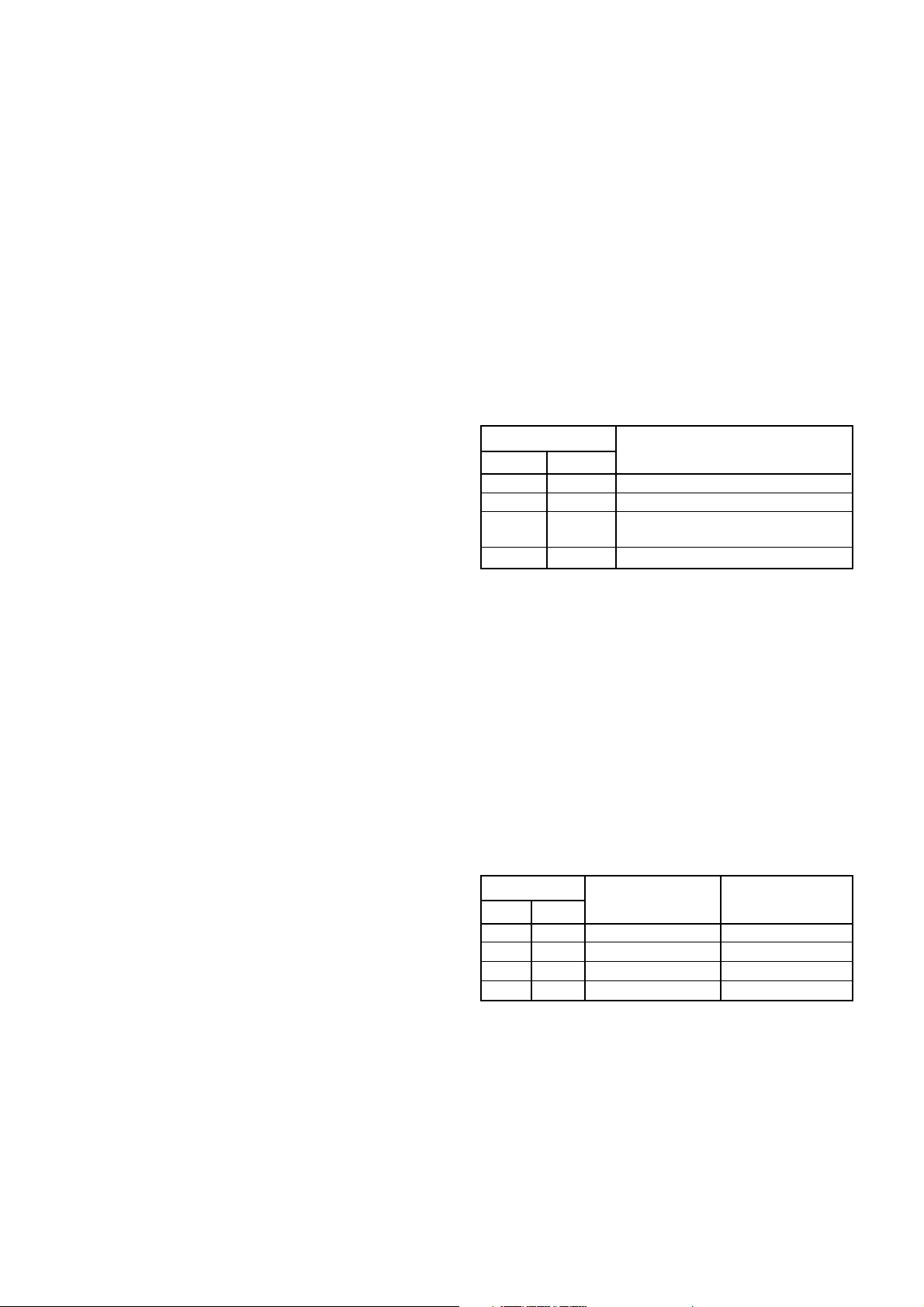
The block diagram of a dual modulus divider arrangement
is shown in Fig. 5. The N/N11 prescaler, together with the
A and M dividers, divide the RF input frequency down to the
comparison frequency at the phase detector input. The
comparison frequency, F
loop synthesiser; when A is incremented (or decremented) by
one, the loop output frequency automatically increments (or
decrements) by F
Hz. When the dividers are reset, at the
REF
end of each count cycle, the modulus of the prescaler is set
to N11 and the input frequency to the A and M dividers is then
RFinput 4(N11) Hz. The output of the A counter controls the
prescaler modulus, which is set to N when A reaches its
programmed value. The M divider continues to count at the
rate RFinput 4N until it reaches its programmed value, at
which point the dividers are reset and the count cycle starts
again. The division ratio of this arrangements is therefore
A(N11) 1 (M2A)N = MN1A
It is evident that for this arrangement to work M must
always be programmed greater than or equal to A and A must
be able to count to N21. These restrictions set a minimum
count of N
2
2N; below this value some division ratios will not
be available.
The SP8858 prescaler can be set to 48/9 or 416/17 mode
by setting the appropriate bit of the reference word. The
A divider is a 4-bit counter, whilst the M divider is a 15-bit
counter. The minimum division ratio, with the 8/9 prescaler, is
2
8
28 = 56, whilst the maximum division ratio, with the 16/17
prescaler, is 16(2
15
21)1(2421) = 524287.
If the 8/9 prescaler is used the MSB of the A counter must
be programmed to 0 and the maximum RF input frequency
must be reduced to 750MHz.
Reference Source and Divider
The reference source for the SP8858 is obtained from an
on-chip oscillator, stabilised by an external quartz crystal. The
oscillator circuit will also function as a buffer amplifier if an
external reference is preferred. In the latter case the signal,
should be AC coupled into pin 20 (see Fig. 12).
The reference oscillator drives a divider stage, the output
of which is the reference signal to the phase comparator. The
PLL controls the input voltage to an external VCO so that the
divided VCO signal is phased locked to this reference signal.
The dynamics of the control loop are determined by the
external loop filter.
The 13-bit reference divider is fully programmable and can
be set to any ratio between 1 and 8191. The programmed
word is stored in the internal reference buffer.
, sets the resolution of a single
REF
reference current into pin 24 (RPD). An external
transimpedance amplifier is required to provide the voltage
drive to the VCO. This requirement is usually performed by
the loop filter operational amplifier which is designed to
provide a type II third order control loop.
Data Entry and Control
The SP8858 is programmed using the serial data interface.
Data is entered into the chip on the DATA pin and clocked into
the internal shift register by the positive going edge of the
CLOCK signal with the ENABLE pin held high. While ENABLE
is high, changes to the shift register will not affect the current
count cycle. On the falling edge of ENABLE the data held in
the shift register is transferred to one of the three buffers (F1,
F2 or reference). Fig. 4 shows the timing requirements for
these three signals.
The 2 LSBs of the 24-bit shift register, C1 and C2, determine
which of the three buffers is loaded with the data held in the
remaining 22 bits as shown in Table 2.
2-bit SR contents
C2 C1
0
1
0
0
0
1
F1
F2
Active A (only the A divider of the
active buffer is changed)
1
1
Reference
Table 2
If the F1 buffer (C2 = 0, C1 = 0) is selected the 22 MSBs
of the shift register are transferred to it. 19 bits of the buffer
provide the data for the A and M dividers; the three remaining
bits control the charge pump current multiplication factor and
the sense of the phase detector. The F2 buffer performs the
same function so that an alternative divider word and/or
phase detector gain can be stored.
The CP current can be multiplied by up to four times by
programming bits G1 and G2 as shown in Table 3. The
maximum charge pump output current is 62mA.
The reference current can be set by resistor RPD
connected between V
Ipin 24 = (V
I
= G3Ipin 24 (G is multiplication factor)
OUT
CC
and pin 24 so that:
CC
21·5)/RPD
Phase detector gain, KPD = I
See Applications, Loop Filter Design
Buffer loaded
/2p A/rad
OUT
Phase Comparator and Charge Pump
The digital phase detector is sensitive to frequency and
phase errors. The basic circuit for a conventional digital
phase/frequency detector is based on two D type flip-flops.
Initially the flip-flops are reset, each one is then set by the
respective pulses of the M and R divider outputs. When both
flip-flops have been set they are immediately reset. In this way
the output of one flip-flop is a pulse whose width is proportional
to phase difference, whilst the second flip-flop is a narrow
pulse determined by the time to reset. The phase detector
outputs drive a charge pump amplifier. One output controls a
constant current source, the other an identical current sink
connected to the same node (CP output, pin 25). The SP8858
phase/frequency detector has been modified and improved to
provide a linear characteristic, thus eliminating deadband
effects.
The phase detector gain is determined by the output
current from the charge pump (±I
) which is set by a
OUT
6
F1 or F2 word
G2 G1
0
1
0
1
0
0
1
1
Charge pump 1
current (
µA)
50
75
125
200
Charge pump 2
multiplier
1
1·5
2·5
4
Table 3 Charge pump currents
When the SENSE bit is set to 1 the inputs and clocks to the
phase detector flip-flops are reversed. The bit should be set
to 1 for a VCO with a positive frequency v. voltage characteristic.
The sense bit also swaps the outputs FREF and FPD on pins
4 and 5. Fig. 1 shows the pin-out for SENSE = 0.
The active buffer, i.e. the one that is currently used to
update the dividers, is selected at pin 13 (F1/F2). A high on
this pin selects F1. The F2 word can be updated while F1 is
 Loading...