MITEL SP8830 Datasheet

SP8830
1.5GHz ÷ 10 Prescaler
Advance Information
DS3690 Issue 3.3 June 1999
Features
● High Speed Operation 1·5GHz
● Silicon Technology for Low Phase Noise (Typically
Better Than 2140dBc / Hz at 10kHz)
● Very Low Power Dissipation: 150mW (Typ.)
●
Single 5V Supply Operation
● High Input Sensitivity
● Very Wide Operating Frequency Range
● Available as DESC SMD 5962 - 9157201MPA
Description
The SP8830 is one of a range of very high speed low
power prescalers for professional and military
applications. The device features a complementary output
stage with on chip current sources for the emitter follower
outputs.
Ordering Information
SP8830 A DG
SP8830 B DG
DES9157201/AC/DGAZ (SMD)
● Temperature Range: 255°C to 1125°C (A Grade)
240°C to 185°C (B Grade)
Absolute Maximum Ratings
Supply voltage, V
CC
Clock input voltage 2.5V p-p
Storage temperature range 65° C to +150°C
Junction temperature + 175°C
- 6.5V
INPUT
INPUT
1
V
CC
1·25k 1·25k
1k 2k
7
OUTPUT
6
OUTPUT
42 45
2
0·8mA
3
0·8mA
1mA
5
GND
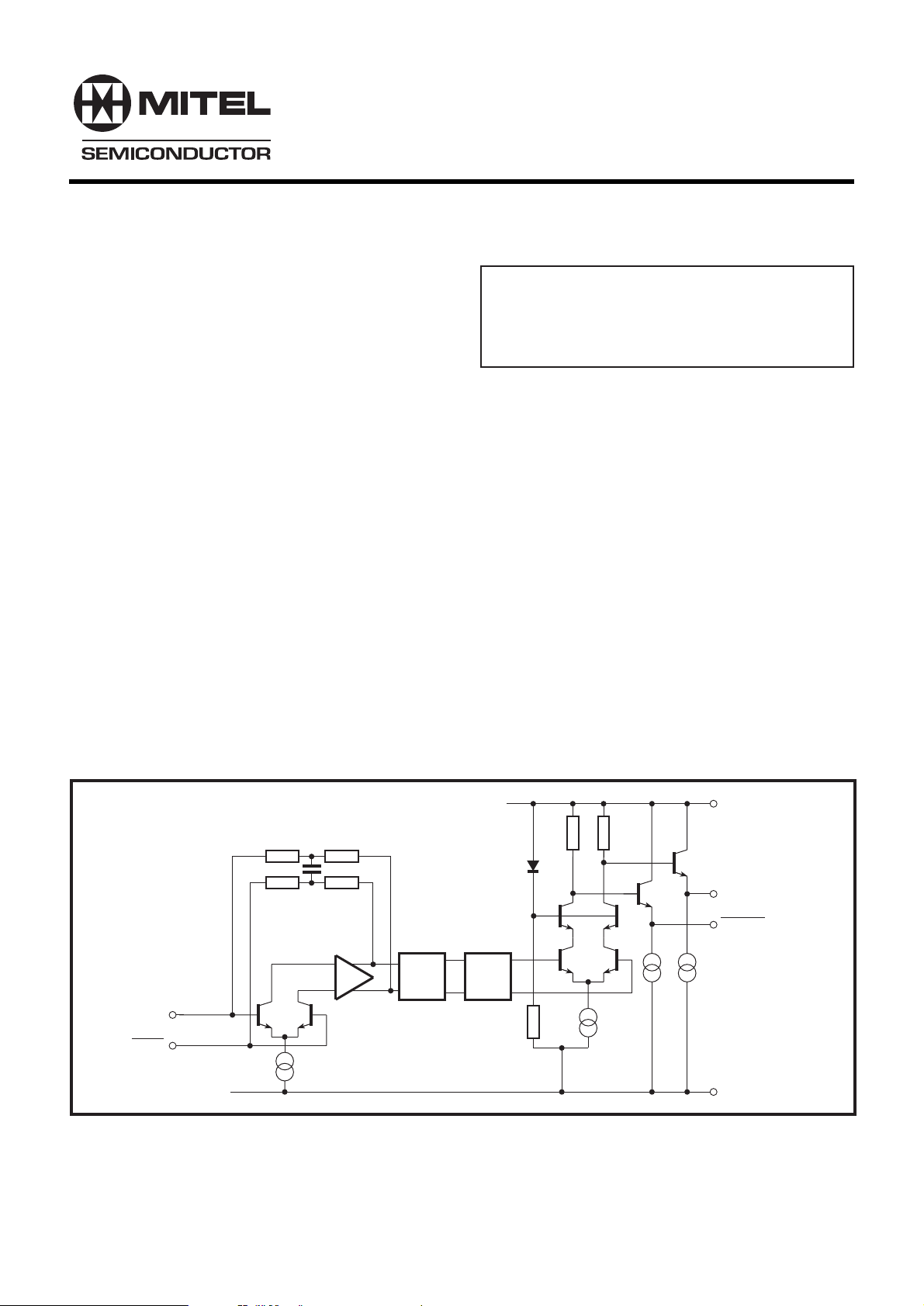
Figure 1 SP8830 block diagram

SP8830 Advance Information
(
)
V
CC
INPUT
INPUT
NC
1
2
3
4
8
7
6
5
NC
OUTPUT
OUTPUT
GND
DG8
Figure 2 Pin connections
Electrical Characteristics
Unless otherwise stated, the Electrical Characteristics are guaranteed over specified supply, frequency and
temperature range
Supply voltage, VCC -4·75V to +5·25V
Temperature, T
Characteristic
Supply current, I
Input sensitivity, 100MHz to
1500MHz
= -55°C to +125°C (A Grade), -40°C to +85°C (B Grade)
AMB
Value
Typ. Max.
40
50
100mAmV
CC
Pin
Min.
1
2, 3
Units
Conditions
RMS sinewave, measured in 50Ω
system. See Figs 3 and 4.
Input impedance (series equivalent)
Output voltage with fIN = 100MHz
Output voltage with fIN = 1500MHz
400
150
100
(mV RMS INTO 50 Ω )
IN
V
50
2, 3
6, 7
0·7
6, 7
GUARANTEED
OPERATING
WINDOW
50
2
1
0·4
*
Ω
pF
V p-p
V p-p
See Fig. 5
*
Tested as specified
in table of Electrical
Characteristics
100 500 1000 1500 2000
FREQUENCY
MHz
Figure 3 Typical input sensitivity
2
 Loading...