MITEL SP8402 Datasheet

SP8402
The SP8402 is a very low phase noise divider which divides
by powers of two. The S0, S1, S2 data inputs select the division
ratio in the range 21 to 28. Special circuits techniques have been
used to reduce the phase noise considerably below that
produced by standard dividers. The data inputs are CMOS or
TTL compatible.
The SP8402 is packaged in a 28 pin plastic SO package to
be compatible with the SP8400 and SP8401 devices.
FEATURES
■ Very low Phase Noise (Typically -155 to 160dBc/Hz at 1kHz
offset)
■ Supply Voltage 5V
ABSOLUTE MAXIMUM RATINGS
Supply Voltage 6.5V
Output Current 20mA
Storage Temperature Range -55°C to +125°C
Maximum Clock Input Voltage 2.5V p-p
ORDERING INFORMATION
SP8402 KG MPES (Commercial Grade)
Very Low Phase Noise Divider by 2
DS3738 - 2.1 March 1994
N/C
N/C
N/C
+5V
V
CC
GND
INPUT
CLOCK
CLOCK INPUT
CLOCK INPUT
INPUT
CLOCK
GND
V
+5V
CC
+5V
V
CC
N/C
S0
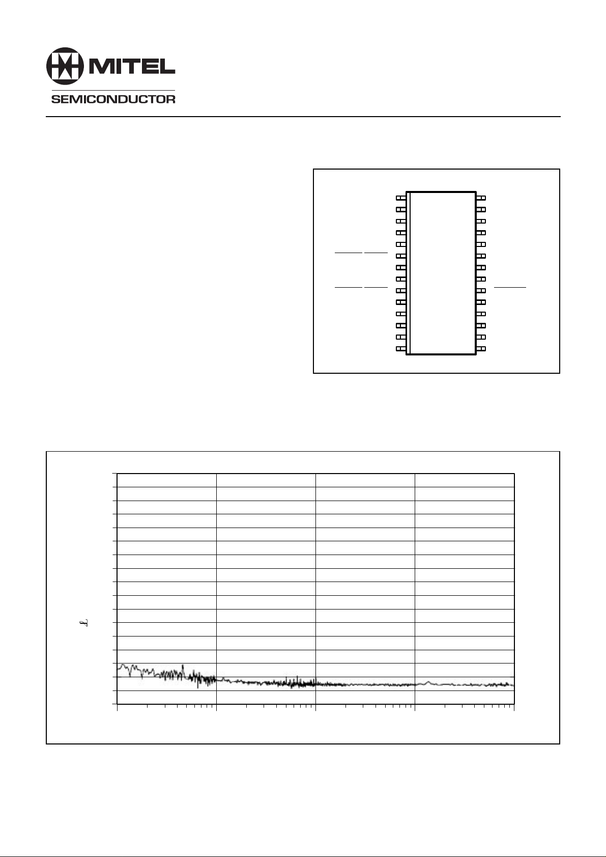
Fig.1 Pin connections - top view
1
2
3
4
5
6
7
8
9
10
11
12
13
14 15
28
27
26
25
24
23
22
21
20
19
18
17
16
N/C
N/C
N/C
N/C
N/C
N/C
N/C
OUTPUT
OUTPUT
N/C
V
+5V
CC
N/C
S2
S1
MP28
N
0
–10
–20
–30
–40
–50
–60
–70
–80
–90
–100
(f) (dBc/Hz) –3dB
–110
–120
–130
–140
–150
–160
–170
10 100 1k 10k 100k
Frequency (Hz)
Fig.2 Typical single sideband phase noise measured at 768MHz

SP8400
ELECTRICAL CHARACTERISTICS
Guaranteed over: Supply voltage VCC = +4.75V to +5.25V Temperature T
Tested at +4.75V and +5.25V at T
= +25°C
amb
= -10°C to +75°C
amb
Characteristic
Supply current
Output voltage swing
Input sensitivity 200MHz to 1.5GHz
Data Inputs
Logic high voltage
Low low voltage
Input current
600
500
400
300
mV rms
in
V
200
100
Pin
4, 11, 12, 18
20, 21
7, 8
Value
Min. Typ. Max.
92
82
320
102
410
140
(-4)
2.2
0.8
180
OPERATING WINDOW
Units
mA
mV
mV
dBm
V
V
µA
Conditions
Output loaded with 300R See Fig.5
p-p @ 1.4GHz input ÷ 256 mode
outputs loaded with 330R See Fig.5
RMS Sine wave into 50 Ohms
(dBm equivalent) See Fig.3
5V Data input voltage
355mV
140mV
0 200 400 600 800 1000 1200 1400
FREQUENCY MHz
1600
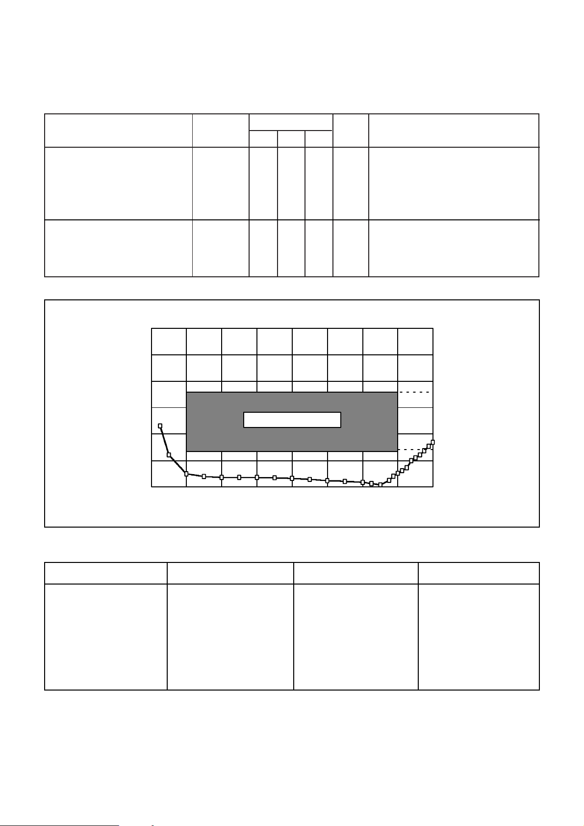
Fig.3 Typical input sensitivity
S0
L
H
L
H
L
H
L
H
S1
L
L
H
H
L
L
H
H
S2
L
L
L
L
H
H
H
H
DIVISION RATIO
2
4
8
16
32
64
128
256
Fig.4 Truth table
2
 Loading...