MITEL SP5848, SP5848KG, SP5848QP1S, SP5848QP1T Datasheet

1
Preliminary Information SP5848
SP5848
2.2/1.3GHz 3-Wire Bus Dual Low Phase Noise PLL
Preliminary Information
Features
● Dual independent PLL frequency synthesisers in a
single package, optimised for double conversion
cable tuners, offering improved application
● 2.2GHz up-synthesiser optimised for low phase
noise up to comparison frequencies of 4MHz
Ordering Information
SP5848/KG/QP1S
SP5848/KG/QP1T
Applications
● TV, VCR, and cable tuning systems
The SP5848 is a dual PLL frequency synthesizer
controlled by a 3-wire bus optimised for application in
double conversion tuners.
Each synthesiser loop within the SP5848 is
independently addressable and contains an RF
programmable divider, phase/frequency detector and
charge pump/loop amplifier section; a common
reference frequency oscillator and divider chain is
provided, whose ratios for each loop are independently
programmable.
Both synthesisers are optimised for low phase noise
performance and in addition synthesiser 2 is capable of
operation with a low comparison frequency.
● 1.3GHz down-synthesiser optimised for low phase
noise AND small step size
● Common reference oscillator and divider with
independently selectable ratios for each
synthesiser
● 10:1 programmable charge pump current ratio in up
synthesiser
● 3-Wire bus programmable, each synthesiser
indepently addressable
● Low power consumption, typ 100mW at 5V
● ESD protection, (Normal ESD handling procedures
should be observed)
DS5076 Issue 1.6 October 1999
Description
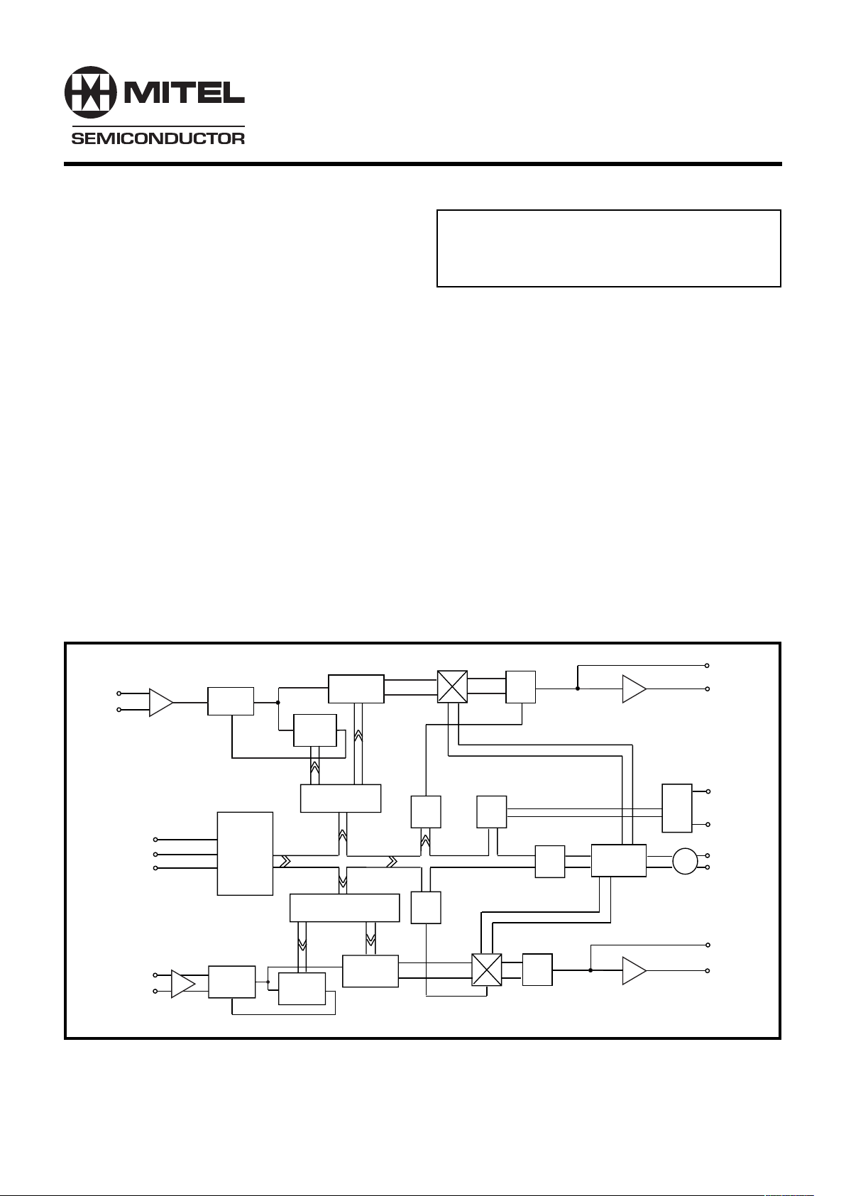
RF1 INPUT
16/17
4 BIT
COUNT
11 BIT
COUNT
15 BIT LATCH
2 BIT
LATCH
PORT P0
PUMP 1
DRIVE 1
16 BIT LATCH
DATA
CLOCK
ENABLE
2
DATA
INTERFACE
RF 2 INPUT
16/17
4 BIT
COUNT
12 BIT
COUNT
1 BIT
LATCH
2 BIT
LATCH
5 BIT
LATCH
9
DIVIDE
PORT P1
PUMP 2
DRIVE 2
Figure 1 Block Diagram

2
SP5848 Preliminary Information
Figure 2 Pin Connections
QP20
PORT P1
CHARGE PUMP 2
DRIVE 2
Vee 2
RF2 INPUT
RF2 INPUT
Vcc2
CRYSTAL
CRYSTAL CAP
Vee
PORT P0
CHARGE PUMP 1
DRIVE 1
Vee 1
RF1 INPUT
RF1 INPUT
Vcc1
ENABLE
DATA
CLOCK
Electrical Characteristics
T
amb
= -40oC to +80oC, Vcc = 4.5 to 5.5 V, These characteristics are guaranteed by either production test or design.
They apply within the specified ambient temperature and supply voltage unless otherwise stated.
Characteristic Pin Value Units Conditions
Min Typ Max
Supply voltage 7, 14 4.5 5.5 V
Supply current 18 22 mA
Synthesiser 1 (UP)
RF1 input voltage 15,16 40 300 mV
rms
80 -2200MHz
RF1 input impedance 15,16 See Figure 4
RF1 division ratio 240 32767
Reference division 1 See Table 1
ratio
Comparison frequency 1 4 MHz
Equivalent phase noise -148 dBc/Hz SSB, within loop bandwidth, all
at phase detector 1 comparison frequencies
Charge pump 1 output 19 See Table 3
current Vpin 19=2V
Charge pump 1 output 19 ±3 ±10 nA Vpin19 = 2V
leakage
Charge pump 1 drive 18 0.5 mA Vpin 18 = 0.7V
output current

3
Preliminary Information SP5848
Electrical Characteristics (continued)
T
amb
= -40oC to +80oC, Vcc = 4.5 to 5.5 V, These characteristics are guaranteed by either production test or design.
They apply within the specified ambient temperature and supply voltage unless otherwise stated.
Characteristic Pin Value Units Conditions
Min Typ Max
Synthesiser 2 (DOWN)
RF2 input voltage 5,6 30 300 mV
rms
80 -1300MHz
RF2 input impedance 5,6 See Figure 5
RF2 division ratio 240 65535
Reference division 2 See Table 2
ratio
Comparison frequency 2 16.25 4000 KHz Phase noise degrades above
250KHz
Equivalent phase noise -144 dBc/Hz SSB, within loop bandwidth, all
at phase detector 2 comparison frequencie up to
250KHz
Charge pump 2 output 2 See Table 4
current Vpin 2=2V
Charge pump 2 output 2 ±3 ±10 nA Vpin2 = 2V
leakage
Charge pump 2 drive 3 0.5 mA Vpin 3 = 0.7V
output curent
Data, clock and enable 12,11,13
Input high voltage 3 Vcc V
Input low voltage 0 0.7 V
Input current -10 10 µA All input conditions
hysterysis 0.8 Vpp
Clock rate 11 500 KHz
Bus timing Data set up 300 ns
Data hold 600 ns
Enable setup 300 ns
Enable hold 600 ns
Clock to enable 300 ns
Reference Oscillator
Crystal frequency 8, 9 2 16 MHz See Figure 6 for application
External reference input 8 2 20 MHz Sinewave coupled through
frequency 10nF blocking capacitor
External reference drive 8 0.2 0.5 Vpp Sinewave coupled through 10nF
blocking capacitor
Outputs ports P0 - P1 1, 20 See note 1
sink current 2 mA Vport = 0.7V
leakage current 10 µA Vport = Vcc
Note 1 Output ports high impedance on power up, with data, clock and enable at logic 0
 Loading...