MITEL SP5769QP1T, SP5769A, SP5769KG, SP5769MP1S, SP5769QP1S Datasheet

DS4878 Issue 4.0 October 1999
SP5769
3GHz I2C Bus Synthesiser
Preliminary information
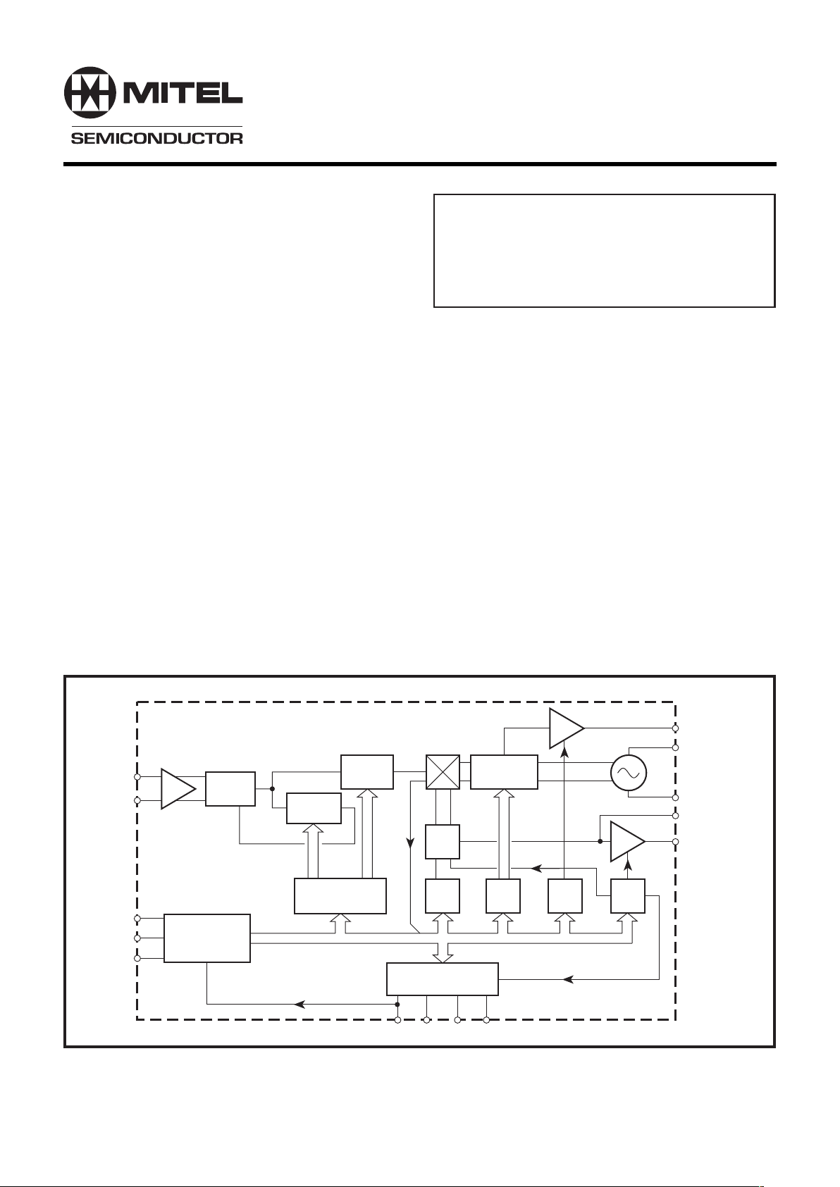
Figure 1 SP5769 block diagram
Ordering Information
SP5769A/KG/MP1S (Tubes)
SP5769A/KG/MP1T (Tape and Reel)
SP5769A/KG/QP1S (Tubes)
SP5769A/KG/QP1T (Tape and Reel)
Features
● Complete 3·0 GHz Single Chip System
● Optimised for Low Phase Noise, with Comparison
Frequencies up to 4 MHz
● No RF Prescaler
● Selectable Reference Division Ratio
● Selectable Reference/Comparison Frequency Output
● Selectable Charge Pump Current with 10:1 Ratio
● Four Selectable I
2
C Addresses
● I
2
C Fast Mode Compliant with 3·3V and 5V Logic Levels
● Four Switching Ports
● Functional Replacement for SP5659 (except ADC)
● Pin Compatible with SP5655
● Power Consumption 110mW with V
CC
= 5·5V, all Ports off
● ESD Protection 2kV min., MIL-STD-883B Method 3015
Cat.1 (Normal ESD handling procedures should be
observed)
Applications
● Digital Satellite and Cable Tuning Systems
● Communications Systems
The SP5769 is a single chip frequency synthesiser
designed for tuning systems up to 3GHz. The RF
preamplifier interfaces direct with the RF programmable
divider, which is of MN1A construction so giving a step
Absolute Maximum Ratings
All voltages are referred to VEE = 0V
Supply voltage, V
CC
RF differential input voltage
All I/O port DC offsets
SDA and SCL DC offset
Storage temperature
Junction temperature
MP16 thermal resistance
Chip to ambient, θ
JA
Chip to case, θ
JC
0·3V to 17V
2·5Vp-p
20·3 to VCC 10·3V
20·3 to 6V
255°C to 1125°C
1150°C
80°C/W
20°C/W
size equal to the loop comparison frequency and no
prescaler phase noise degradation over the full RF
operating range. The comparison frequency is obtained
either from an on-chip crystal controlled oscillator, or from
an external source. The oscillator frequency, f
REF
, or phase
comparator frequency, f
COMP
, can be switched to the REF/
COMP output providing a reference for a second frequency
synthesiser. The synthesiser is controlled via an 12C bus
4-BIT LATCH AND
PORT INTERFACE
4
16/17
4-BIT
COUNT
11-BIT
COUNT
15-BIT LATCH
REFERENCE
DIVIDER
REF/COMP
CRYSTAL CAP
CRYSTAL
CHARGE PUMP
DRIVE
I2C BUS
TRANSCEIVER
ADDRESS
SDA
SCL
RF
INPUT
P3
11
2
3
1
16
6
13
14
10
4
5
PUMP
2 BIT 4 BIT 2 BIT 3 BIT
789
P2 P1 P0
CP TEST
MODE SET
LOCK
f
PD
/2
f
PD
/2 SELECT
ENABLE/
SELECT

2
SP5769
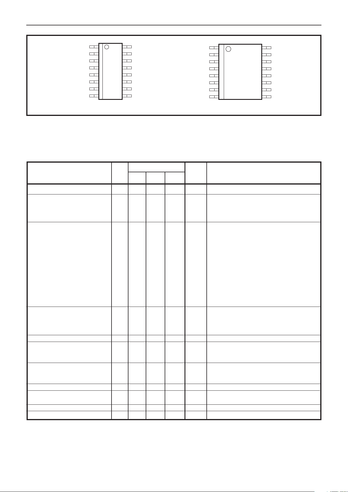
Figure 2 Pin connections - top view
Electrical Characteristics
Test conditions (unless otherwise stated): T
AMB
= 240°C to 180°C, VCC = 4·5V to 5·5V. These characteristics are
guaranteed by either production test or design. They apply within the specified ambient temperature and supply
voltage ranges unless otherwise stated.
Characteristic Conditions
Max.
Min.
Value
Typ.
Units
100MHz to 200MHz
200MHz to 3GHz
See Figure 4
5V I2C logic selected
3·3V I2C logic selected
5V I2C logic selected
3·3V I2C logic selected
Input voltage = V
CC
Input voltage = V
EE
V
CC
= V
EE
I
SINK
= 3mA
I
SINK
= 6mA
See Table 6, V
PIN1
= 2V
V
PIN1
= 2V, VCC = 15·0V, T
AMB
= 25°C
V
PIN16
= 0·7V
See Figure 5 for application
Sinewave coupled via 10nF blocking capacitor
Sinewave coupled via 10nF blocking capacitor
AC coupled, see Note 2
0·0625 to 20MHz
Enabled by bit RE = 1
SSB, within loop bandwidth, all comparison
frequencies
See Table 1
Pin
25
300
300
5·5
5·5
1·5
1
10
210
10
0·4
0·6
400
610
20
20
0·5
4
32767
Supply current
RF input
Input voltage
Input impedance
SDA, SCL
Input high voltage
Input low voltage
Input high current
Input low current
Leakage current
Input hysteresis
SDA output voltage
SCL clock rate
Charge pump
Output current
Output leakage
Drive output current
Crystal frequency
External reference
Input frequency
Drive level
Buffered REF/COMP
Output amplitude
Output impedance
Comparison frequency
Equivalent phase noise at
phase detector
RF division ratio
Reference division ratio
12
13,14
4,5
4
5
1
1
16
2,3
3
11
100
40
3
2·3
0
0
0·4
0·5
2
2
0·2
2148
240
20
63
0·35
250
mA
mVrms
mVrms
V
V
V
V
µA
µA
µA
V
V
V
kHz
nA
mA
MHz
MHz
Vp-p
Vp-p
Ω
MHz
dBc/Hz
cont…
MP16
SP
5769
1
2
3
4
5
6
7
8
16
15
14
13
12
11
10
9
CHARGE PUMP
CRYSTAL CAP
CRYSTAL
SDA
SCL
PORT P3/LOGLEV
PORT P2
PORT P1
DRIVE
V
EE
RF INPUT
RFINPUT
V
CC
REF/COMP
ADDRESS
PORTP0
QP16
16
15
14
13
12
11
10
9
1
2
3
4
5
6
7
8
SP
5769
CHARGE PUMP
CRYSTAL CAP
CRYSTAL
SDA
SCL
PORT P3/LOGLEV
PORT P2
PORT P1
DRIVE
V
EE
RF INPUT
RFINPUT
V
CC
REF/COMP
ADDRESS
PORTP0

3
SP5769
Electrical Characteristics (continued)
2
3
0
Characteristic
V
PORT
= 0·7V
V
PORT
= V
CC
See Note 1
See Table 3
VIN = V
CC
VIN = V
EE
See Note 3
5V I2C logic level selected or open circuit
3·3V I2C logic level selected
VIN = V
EE
to V
CC
Conditions
Max.
Min.
Value
Units
mA
µA
mA
µA
V
V
µA
Typ.
10
1
20·5
1·5
10
Output Ports P3 - P0
Sink current
Leakage current
Address select
Input high current
Input low current
Logic level select
Input high level
Input low level
Input current
Pin
6-9
10
6
NOTES
1. Output ports high impedance on power-up, with SDA and SCL at logic ‘0’.
2. If the REF/COMP output is not used, the output should be left open circuit or connected to VCC and disabled by setting RE = ‘0’.
3. Bi-dectional port. When used as an output, the input logic state is ignored. When used as an input, the port should be switched into
high impedance (off) state.
Functional Description
The SP5769 contains all the elements necessary, with the
exception of a frequency reference, loop filter and external
high voltage transistor, to control a varactor tuned local
oscillator, so forming a complete PLL frequency
synthesised source. The device allows for operation with
a high comparison frequency and is fabricated in high
speed logic, which enables the generation of a loop with
good phase noise performance.
The RF input signal is fed to an internal preamplifier, which
provides gain and reverse isolation from the divider signals.
The output of the preamplifier interfaces with the 15-bit
fully programmable divider which is of MN1A architecture,
where the dual modulus prescaler is 416/17, the A counter
is 4 bits, and the M counter is 11 bits.
The output of the programmable divider is applied to the
phase comparator where it is compared in both phase and
frequency domains with the comparison frequency. This
frequency is derived either from the on-chip crystal
controlled oscillator or from an external reference source.
In both cases the reference frequency is divided down to
the comparison frequency by the reference divider which
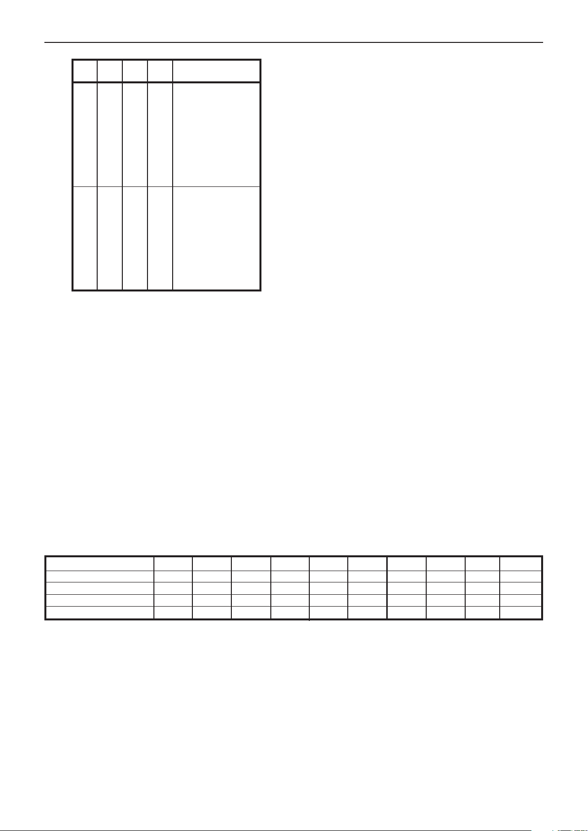
is programmable into 1 of 16 ratios as detailed inTable 1.
The output of the phase detector feeds a charge pump
and loop amplifier section, which when used with an
external high voltage transistor and loop filter, integrates
the current pulses into the varactor line voltage. The
programmable divider output fPD/2 can be switched to port
P0 by programming the device into test mode. The test
modes are described inTable 5.
Programming
The SP5769 is controlled by an I2C data bus and is
compatible with both standard and fast mode formats and
with I2C data generated from nominal 3·3V and 5V sources.
The I2C logic level is selected by the bi-directional port
P3/ LOGLEV. 5V logic levels are selected by connecting
P3/ LOGLEV to VCC or leaving it open circuit; 3·3V logic
levels are set by connecting P3/LOGLEV to ground. If this
port is used as an input the P3 data should be programmed
to high impedance. If used as an output only 5V logic levels
can be used, in which case the logic state imposed by the
port on the input is ignored.
Data and clock are fed in on the SDA and SCL lines
respectively as defined by I2C bus format . The synthesiser
can either accept data (write mode), or send data (read
mode). The LSB of the address byte (R/W) sets the device
into write mode if it is low, and read mode if it is high.
Tables 2 and 3 illustrate the format of the data. The device
can be programmed to respond to several addresses,
which enables the use of more than one synthesiser in an
I2C bus system. Table 4 shows how the address is selected
by applying a voltage to the address input. When the device
receives a valid address byte, it pulls the SDA line low
during the acknowledge period, and during following
acknowledge periods after further data bytes are received.
When the device is programmed into read mode, the
controller accepting the data must be pulled low during all
status byte acknowledge periods to read another status
byte. If the controller fails to pull the SDA line low during
this period, the device generates an internal STOP
condition, which inhibits further reading.

4
SP5769
0
0
0
0
0
0
0
0
1
1
1
1
1
1
1
1
R3
0
0
0
0
1
1
1
1
0
0
0
0
1
1
1
1
R2
0
0
1
1
0
0
1
1
0
0
1
1
0
0
1
1
R1
0
1
0
1
0
1
0
1
0
1
0
1
0
1
0
1
R0 Division ratio
byte data is retained. To facilitate smooth fine tuning, the
frequency data bytes are only accepted by the device after
all 15 bits of frequency data have been received, or after
the generation of a STOP condition.
Read mode
When the device is in read mode, the status byte read
from the device takes the form shown in Table 3.
Bit 1 (POR) is the power-on reset indicator, and this is set
to a logic ‘1’ if the VCC supply to the device has dropped
below 3V (at 25°C ), e.g. when the device is initially turned
on. The POR is reset to ‘0’ when the read sequence is
terminated by a STOP command. When POR is set high
this indicates the programmed information may be
corrupted and the device reset to power up condition.
Bit 2 (FL) indicates whether the device is phase locked, a
logic’1’is present if the device is locked, and a logic ‘0’ if it
is not.
Programable features
● RF programmable divider Function as described
above.
● Reference programmable divider Function as
described above.
● Charge pump current The charge pump current can
be programmed by bits C1 and C0 within data byte 5,
as defined in Table 6.
● Test mode The test modes are invoked by setting bit
T2 = 1, with selected test modes as defined by bits T1
and T0 as described in Table 5. Clock input on crystal
and RF input pins are required to invoke FL test modes.
● Reference/Comparison frequency output The
reference frequency f
REF
or comparison frequency f
COMP
can be switched to the REF/COMP output, function as
defined in Table 7. RE and RS default to logic’1’during
device power up, thus enabling the comparison
frequency f
COMP
at the REF/COMP output.
Write mode
With reference to Table 2, bytes 2 and 3 contain frequency
information bits 214-20 inclusive. Bytes 4 and 5 control the
reference divider ratio (see Table 1), charge pump setting
(see Table 6), REF/COMP output (see Table 7), output
ports and test modes (see Table 5).
After reception and acknowledgement of a correct address
(byte 1), the first bit of the following byte determines whether
the byte is interpreted as a byte 2 or 4, a logic ‘0’ indicating
byte 2, and a logic ‘1’ indicating byte 4. Having interpreted
this byte as either byte 2 or 4, the following data byte will
be interpreted as byte 3 or 5 respectively. Having received
two complete data bytes, additional data bytes can be
entered, where byte interpretation follows the same
procedure, without re-addressing the device. This
procedure continues until a STOP condition is received.
The STOP condition can be generated after any data byte,
if however it occurs during a byte transmission, the previous
Table 1 Reference division ratios
2
4
8
16
32
64
128
256
24
5
10
20
40
80
160
320
Address
Programmable divider
Programmable divider
Control data
Control data
1
0
2
7
1
C1
Byte 1
Byte 2
Byte 3
Byte 4
Byte 5
1
2
14
2
6
T2
C0
0
2
13
2
5
T1
RE
0
2
12
2
4
T0
RS
0
2
11
2
3
R3
P3
MA1
2
10
2
2
R2
P2
MA0
2
9
2
1
R1
P1
0
2
8
2
0
R0
P0
A
A
A
A
A
Table 2 Write data format (MSB transmitted first)
MSB LSB
A Acknowledge bit
MA1, MA0 Variable address bits (see Table 4)
214-2
0
Programmable division ratio control bits
R3-R0 Reference division ratio select (see Table 1)
C1, C0 Charge pump current select (see Table 6)
RE Reference oscillator output enable
RS REF/COMP output select when RE=1 (see Table 7)
T2-T0 Test mode control bits (see Table 5)
P3-P0 P3, P2, P1 and P0 port output states
 Loading...