MITEL SP5748KG, SP5748MP1S, SP5748MP1T, SP5748 Datasheet

FEATURES
● Complete 2.4 GHz single chip system
(for faster device refer to to SP5768)
● Optimised for low phase noise, with comparison
frequencies up to 4 MHz
● No RF prescaler
● Selectable reference division ratio
● Reference frequency output
● Selectable charge pump current
● Integrated loop amplifier
● Two switching ports
● Low power replacement for SP5658 and 5668
● Downwards software compatible with SP5658
● ESD protection, (Normal ESD handling
procedures should be observed)
ORDERING INFORMATION
SP5748/KG/MP1S (Tubes)
SP5748/KG/MP1T (Tape and Reel)
The SP5748 is a single chip frequency synthesiser
designed for tuning systems up to 2.4 GHz and is
optimized for low phase noise with comparison
frequencies up to 4 MHz. It is designed to be downwards
software compatible with the SP5658.
The RF programmable divider contains a front end dual
modulus 16/17 functioning over the full operating range
and allows for coarse tuning in the upconverter
application and fine tuning in the downconverter.
Comparison frequencies are obtained either from a
crystal controlled on-chip oscillator or from an external
source. a buffered reference frequency output is also
available to drive a second SP5748.
The device also contains 2 switching ports.
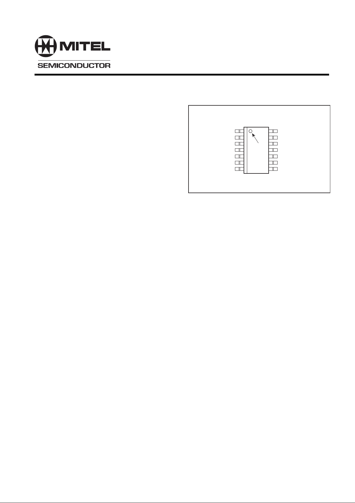
MP14
Figure1 Pin connections - top view
14
SPOT REF.
CHARGE PUMP
CRYSTAL CAP
CRYSTAL
ENABLE
DATA
CLOCK
PORT P1/OC
DRIVE
V
EE
RF INPUT
RF INPUT
V
CC
REF
PORT P0/OP
APPLICATIONS
● TV, VCR and Cable tuning systems
● Communications systems
SP5748
2.4GHz Very Low Phase Noise PLL
Advance Information
DS4875 - 1.3 November 1998

2
SP5748 Advance Information
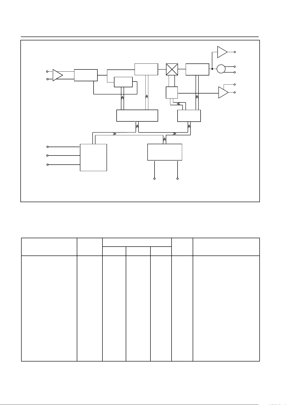
Figure 2 SP5748 block diagram
ELECTRICAL CHARACTERISTICS
These characteristics are guaranteed by either production test or design. They apply within the specified
ambient temperature and supply voltage unless otherwise stated.
T
AMB
= -40°C to 80°C, V
CC
= +4·5V to +5·5V
Characteristic Pin Value Units Conditions
Min Typ Max
Supply current 10 13 mA
RF input frequency range 11,12 80 2400 MHz
RF input voltage 11,12 30 300 mV rms
RF input impedance 11,12 See Figure 3
Data, clock & enable 5,6,4
input high voltage 3 Vcc V
input low voltage 0 0.7 V
input current -10 10 µA All input conditions
hysterysis 0.8 V
PP
PORT P1/OC
RF INPUT
16/17
13 BIT
COUNT
4 BIT
COUNT
REFERENCE
DIVIDER
REF
CRYSTAL
PUMP
DRIVE
17 BIT LATCH 6 BIT LATCH
DATA
CLOCK
ENABLE
DATA
INTERFACE
3 BIT
LATCH & PORT/
TEST MODE
INTERFACE
PORT P0/OP

3
SP5748 Advance Information
ELECTRICAL CHARACTERISTICS (continued)
These characteristics are guaranteed by either production test or design. They apply within the specified
ambient temperature and supply voltage unless otherwise stated.
T
AMB
= -40°C to 80°C, V
CC
=+ 4·5V to +5·5V
Characteristic Pin Value Units Conditions
Min Typ Max
Clock rate 6 500 kHz
Bus timing - 5,6,4 See Figure4
data set up 300 ns
data hold 600 ns
enable set up 300 ns
enable hold 600 ns
clock to enable 300 ns
Charge pump output 1 See Figure 5,
current Vpin1 = 2V
Charge pump output 1 +-3 +-10 nA Vpin1=2V
leakage
Charge pump drive 14 0.5 mA Vpin 14=0.7V
output current
Crystal frequency 2,3 2 20 MHz See Figure 6 for application
Recommended crystal 10 200 Ω 4 MHz parallel resonant
crystal. series resistance
Oscillator temperature TBC ppm/oC
stability
Oscillator supply voltage TBC ppm/V
stability
External reference input 2 2 20 MHz Sinewave coupled through
frequency TBA nF blocking capacitor
External reference drive 2 0.2 0.5 V
pp
Sinewave coupled through
level TBA nF blocking capacitor
Buffered reference 9 AC coupled
frequency output *
output amplitude 0.35 Vpp 2-20MHz
output impedance TBC Ω

4
SP5748 Advance Information
ELECTRICAL CHARACTERISTICS
These characteristics are guaranteed by either production test or design. They apply within the specified
ambient temperature and supply voltage unless otherwise stated.
T
AMB
= -40°C to 80°C, V
CC
= +4·5V to +5·5V
Characteristic Pin Value Units Conditions
Min Typ Max
Comparison frequency 4 MHz
Equivalent phase noise at -148 dBc/Hz @10 kHz, SSB, with 2 MHz
phase detector comparison from 4 MHz crystal
reference
RF division ratio 240 131071
Reference division ratio see figure (7)
Output ports P0-P1# 7, 8
sink current 2 mA Vport = 0.7V
leakage current 10 µA Vport = Vcc
* Reference output disabled by connecting to Vcc if not required
’ Output ports high impedance on power up, with data, clock and enable at logic 0

5
SP5748 Advance Information
The RF signal is fed to an internal preamplifier, which
provides gain and reverse isolation from the divider
signals. The output of the preamplifier is fed to the 17 bit
fully programmable counter, which is of MN+A
architecture. The M counter is 13 bit and the A counter
4
The output of the programmable counter is fed to the
phase comparator where it is compared in both phase
and frequency domain with the comparison frequency.
This frequency is derived either from the on board
crystal controlled oscillator or from an external
reference source. In both cases the reference
frequency is divided down to the comparison frequency
by the reference divider which is programmable into1 of
16 ratios as descried in Figure 7.
The output of the phase detector feeds the charge pump
and loop amplifier section, which when used with an
external high voltage transistor and loop filter integrates
the current pulses into the varactor line voltage. The
charge pump current setting is described in Figure 5,
A buffered crystal reference frequency suitable for
driving further synthesisers is available from pin 9. If not
required this output can be disabled by connecting to
Vcc
The programmable divider output divided by 2, Fpd/2
and comparison frequency, Fcomp can be switched to
ports P0 and P1 respectively by switching the device
into test mode. The test modes are described in Figure
8.
ABSOLUTE MAXIMUM RATINGS
All voltages are referred to VEE at 0V
Characteristic Pin Min Typ Max Units Conditions
Supply voltage, Vcc 10 -0.3 7 V
RF input voltage 11,12 2.5 V
p-p
Differential across pins
11 and 12
RF input DC offset 11,12 -0.3 Vcc+0.3 V
Port voltage 7,8 -0.3 Vcc+0.3 V
Charge pump DC offset 1 -0.3 Vcc+0.3 V
Varactor drive DC offset 14 -0.3 Vcc+0.3 V
Crystal DC offset 2,3 -0.3 Vcc+0.3 V
Buffered ref output 9 -0.3 Vcc+0.3 V
Data, clock & enable 5,6,4 -0.3 Vcc+0.3 V
DC offset
Storage temperature -55 +125 °C
Junction temperature +150 °C
MP14 thermal resistance,
chip to ambient 81 °C/W
chip to case 27 °C/W
Power consumption at TBC mW All ports off
Vcc=5.5V
ESD protection 2 kV Mil-std 883B latest revision
method 3015 cat.1.
Functional description
The SP5748 contains all the elements necessary, with
the exception of a frequency reference, loop filter and
external high voltage transistor, to control a varicap
tuned local oscillator, so forming a complete PLL
frequency synthesised source. The device allows for
operation with a high comparison frequency and is
fabricated in high speed logic, which enables the
generation of a loop with excellent phase noise
performance, even with high comparison frequencies.
The package and pin allocation is shown in Figure 1 and
the block diagram in Figure 2.
The SP5748 is controlled by a standard 3-wire bus
comprising data, clock and enable inputs. The
programming word contains 26 bits, two of which are
used for port selection, 17 to set the programmable
divider ratio, four bits to select the reference division
ratio, bits RD & R0-R2, see Figure 7, two bits to set
charge pump current, bit C0 and C1, see Figure 5, and
the remaining bit to access test modes, bit T0, see
Figure 8. The programming format is shown in Figure 4.
The clock input is disabled by an enable low signal, data
is therefore only loaded into the internal shift registers
during an enable high and is clocked into the controlling
buffers by an enable high to low transition. This load is
also synchronised with the programmable divider so
giving smooth fine tuning.
 Loading...