MITEL SP5730A, SP5730KG, SP5730MP1S, SP5730MP1T, SP5730QP1S Datasheet
...
Features
SP5730
1.3GHz Low Phase Noise Frequency Synthesiser
Preliminary Information
DS4877 issue 1.9 July 1999
● Complete 1.3GHz single chip system for
Digital Terrestrial Television applications
● Selectable reference division ratio, compatible
with (DTT) requirements
● Optimised for low phase noise, with
comparison frequencies up to 4MHz
● No RF prescaler
● Selectable reference/comparison frequency
output
● Four selectable I
2
● I
C fast mode compliant and compatible with
2
C bus address
3.3 and 5V logic levels
● Four switching ports
● ESD protection, (Normal ESD Handling
procedures should be observed)
Applications
● Digital Satellite ,Cable and Terrestrial tuning
systems
● Communications systems
Ordering Information
SP5730A/KG/MP1S Sticks
SP5730A/KG/MP1T Tape and Reel
SP5730A/KG/QP1S Sticks
SP5730A/KG/QP1T Tape amd Reel
Description
The SP5730 is a single chip frequency synthesiser
designed for tuning systems up to 1.3GHz and is
optimised for digital terrestrial applications.
The RF preamplifier interfaces direct with the RF
programmable divider, which is of MN+A construction
so giving a step size equal to the loop comparison
frequency and no prescaler phase noise degradation
over the RF operating range.
The comparison frequency is obtained either from an
on-chip crystal controlled oscillator, or from an external
source. The oscillator frequency, Fref, or phase
comparator frequency, Fcomp, can be switched to the
REF/COMP output providing a reference frequency for
a second frequency synthesiser.
The synthesiser is controlled via an I2C bus and is fast
mode compliant. It can be hard wired to respond to one
of four addresses to enable two or more synthesisers to
be used on a common bus.
The device contains four switching ports P0-P3.

SP5730 Preliminary Information
RF/COMP
enable/select
CRYSTAL
CRYSTAL CAP
RF INPUT
8/9
12 BIT
COUNT
REF DIVIDER
Osc
ADDRESS
SDA
SCL
2
I C BUS
TRANSCEIVER
3 BIT
COUNT
15 BIT LATCH
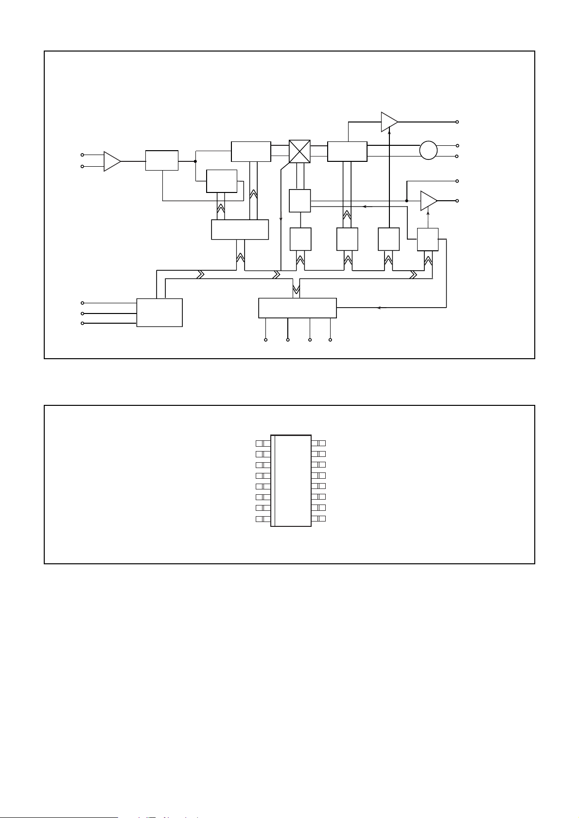
Figure 1 Block diagram
CHARGE PUMP
CRYSTAL CAP
PORT P3/LOGLEV
AGC
IOUT
CRYSTAL
VEEA
SDA
IFINB
SCL
IFIN
IVCCA
PORT P2
QOUT
PORT P1
VEEC
PORT P3
Lock
fpd/2
PUMP
2 BIT
4 BIT LATCH & PORT
INTERFACE
PORT P1
PORT P2
116
SL1711B
c/p
mode
5 BIT 2 BIT 2 BIT
fpd/2 select
PORT P0
DRIVE
VCCB
V
VCODIS
EE
RF INPUT
VCO B
RF INPUT
VCO A
V
CC
VEEB
REF/COMP
PSCAL
ADDRESS
PSCALB
PORT P0
VCCC
CHARGE PUMP
DRIVE
disable
MP16
MP16 & QP16
Figure 2 Pin connections top view
2

Preliminary Information SP5730
Electrical Characteristics
Tamb= -40oC to 85oC, VCC= 4.5 to 5.5V
These characteristics are guaranteed by either production test or design. They apply within the specified
ambient temperature and supply voltage unless otherwise stated.
Characteristic Pin Value Units Conditions
Min Typ Max
Supply current 20 mA
RF input voltage 13,14 12.5 300 mVrms 100 MHz – 1.3GHz, see Figure. 4
RF input voltage 13,14 40 300 mVrms 50MHz - 100MHz, see Figure 4
RF input impedance 13,14 See Figure. 5
SDA, SCL 4, 5
Input high voltage 3 5.5 V 5V I2C logic selected
Input low voltage 0 1.5 V 5V I2C logic selected
Input high voltage 2.3 3.5 V 3V3 I2C logic selected
Input low voltage 0 1 V 3V3 I2C logic selected
Input high current 10 µA Input voltage =Vcc
Input low current 10 µA Input voltage = Vee
Leakage current 10 µA Vee = Vcc
Hysteresis 0.4 V
SDA output voltage 4 0.4 V Isink = 3mA
0.6 V Isink = 6mA
SCL clock rate 5 400 kH
Charge pump output 1 See Table 6 Vpin1 = 2V
current
Charge pump output 1 3 10 nA Vpin1 = 2V, Vcc = 5V, +25°C
leakage
Charge pump drive 16 0.5 mA Vpin16 = 0.7V
output current
Crystal frequency 2,3 2 20 MHz See Figure 3 for application
Recommended crystal 10 200 Ω 4 MHz “parallel resonant”
series resistance crystal.
External reference input 3 2 20 MHz Sinewave coupled through
Frequency 10 nF blocking capacitor
External reference drive 3 0.2 0.5 Vpp Sinewave coupled through
level 10 nF blocking capacitor
3

SP5730 Preliminary Information
Electrical Characteristics (continued)
Tamb= -40oC to 85oC, Vcc= 4.5 to 5.5V
These characteristics are guaranteed by either production test or design. They apply within the specified
ambient temperature and supply voltage unless otherwise stated.
Characteristic Pin Value Units Conditions
Min Typ Max
Buffered REF/COMP output 11 AC coupled 0.5-20MHz
output amplitude 0.35 Vpp Enabled by bit RE= 1
output impedance 250 Ω See note 2
Phase detector Comparison 4 MHz
frequency
Equivalent phase noise at phase dBc/Hz SSB, within loop bandwidth
detector -152 Fcomp = 2MHz
-158 Fcomp = 125kHz
RF division ratio 56 32767
Reference division ratio See Table 1
Output ports P0 - P3 6-9 See Note 1
sink current 2 mA Vport = 0.7
Leakage current 10 µA Vport = Vcc
Address Select 10 See Figure 4 Table 3
Input high current 1 mA Vin = Vcc
Input low current -0.5 mA Vin = Vee
Logic level select 6 See note 3
Input high level 3 Vcc V 5V I2C logic selected, or
open circuit
Input low level 0 1.5 V 3V3 I2C logic selected
Input current -10 10 µA Vin = Vee to Vcc
Notes:
1. Output ports high impedance on power up, with data, clock, and enable at logic ‘0’
2. If the REF/COMP output is not used, the output should be left open circuit or connected to Vcc, and disabled by
setting RE = 0
3. Bi-directional port. When used as an output, the input logic state is ignored. When used as an input the port should
be switched in to high impedance (off) state.
4

Preliminary Information SP5730
Absolute Maximum Ratings
All voltages are referred to Vee at 0V
Characteristic Min Max Units Conditions
Supply voltage, Vcc -0.3 7 V Transient
RF input voltage 2.5 Vpp Differential
All I/O port DC offsets -0.3 Vcc+0.3 V
SDA and SCL DC offset -0.3 6V V
Storage temperature -55 +150
Junction temperature 150
QP16 thermal resistance,
chip to ambient 80 °C/W
chip to case 20 °C/W
Power consumption at 83 mW All ports off
Vcc = 5.5V
ESD protection 2 kV mil std 883 latest revision method 3015
o
C
o
C
class 1
Functional Description
The SP5730 contains all the elements necessary, with
the exception of a frequency reference, loop filter and
external high voltage transistor, to control a varicap
tuned local oscillator, so forming a complete PLL
frequency synthesised source. The device allows for
operation with a high comparison frequency and is
fabricated in high speed logic, which enables the
generation of a loop with good phase noise performance.
It can also be operated with comparison frequencies
appropriate for frequency offsets as required in digital
terrestrial (DTT) receivers The block diagram is shown
in Figure 2.
The RF input signal is fed to an internal preamplifier,
which provides gain and reverse isolation from the
divider signals. The output of the preamplifier interfaces
direct with the 15-bit fully programmable divider, which
is of MN+A architecture, where the dual modulus
prescaler is 8/9, the A counter is 3-bits, and the M
counter is 12 bits.
The output of the programmable divider is fed to the
phase comparator where it is compared in both phase
and frequency domain with the comparison frequency.
This frequency is derived either from the on-board
crystal controlled oscillator or from an external reference
source. In both cases the reference frequency is divided
down to the comparison frequency by the reference
divider which is programmable into 1 of 29 ratios as
detailed in Table 1.
The output of the phase detector feeds a charge pump
and loop amplifier section, which when used with an
external high voltage transistor and loop filter, integrates
the current pulses into the varactor line voltage.
The programmable divider output Fpd divided by two
can be switched to port P0 by programming the device
into test mode. The test modes are described in Table 4.
Programming
The SP5730 is controlled by an I2C data bus and is
compatible with both standard and fast mode formats
and with I2C data generated from nominal 3.3V and 5V
sources. The I2C logic level is selected by the bi-directional
port P3/LOGLEV. 5V logic levels are selected by
connecting P3/LOGLEV to Vcc or leaving open circuit
and 3.3V by connecting to ground. If this port is used as
an input the P3 data should be programmed to high
impedance. If used as an output 5V logic only levels can
be used and in this case the logic state imposed by the
port on the input is ignored.
Data and Clock are fed in on the SDA and SCL lines
respectively as defined by I2C bus format. The synthesiser
can either accept data (write mode), or send data (read
mode). The LSB of the address byte (R/W) sets the
device into write mode if it is low, and read mode if it is
high. Table 2 illustrates the format of the data. The
device can be programmed to respond to several
addresses, which enables the use of more than one
synthesiser in an I2C bus system. Table 3 shows how the
address is selected by applying a voltage to the ‘address’
input.
5
 Loading...