查询SP5658供应商
SP5658
2.7GHz 3-Wire Bus Controlled Frequency Synthesiser
Advance Information
Supersedes October 1996 Media IC Handbook HB3923-2 DS4064 - 4.1 March 1998
The SP5658 is a single chip frequency synthesiser
designed for tuning systems up to 2.7GHz.
The RF preamplifer contains a divide by two prescaler
which can be disabled for applications up to 2GHz so enabling
a step size equal to the comparison frequency up to 2GHz and
twice the comparison frequency up to 2.7GHz.
Comparison frequencies are obtained either from a crystal
controlled on–chip oscillator or from an external source.
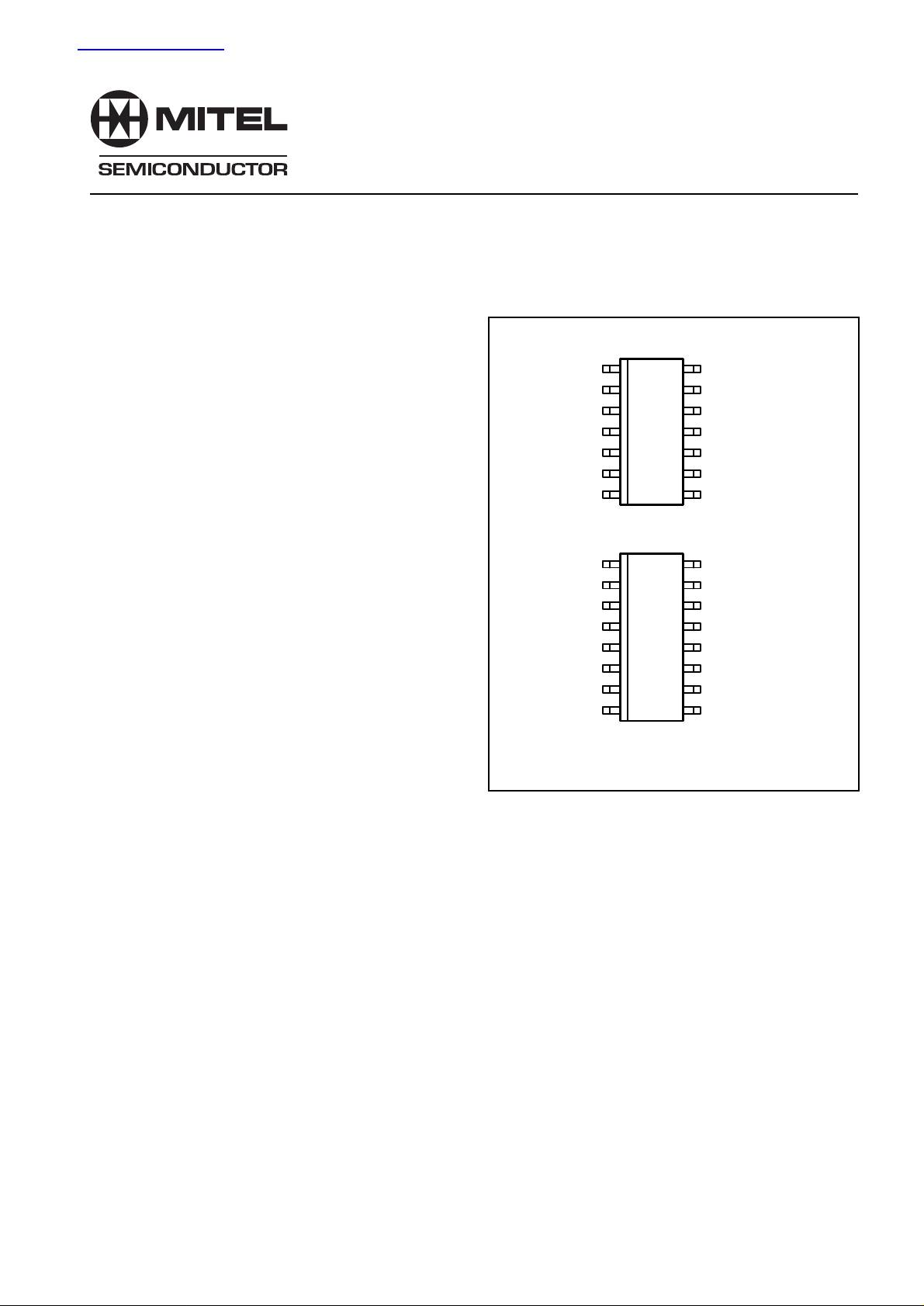
The device contains two switching ports, in the 14 pin
version and four in the 16 pin, together with an ‘‘in–lock” flag
output. The device also contains a varactor line disable and
charge pump disable facility.
FEATURES
■ Complete 2.7GHz single chip system
■ Optimised for low phase noise
■ Selectable divide by two prescaler
■ Selectable reference division ratio
■ Charge pump disable
■ Varactor line disable
■ ‘In–lock’ flag
■ Two switching ports in 14 pin version
■ Four switching ports in 16 pin version
■ Pin compatible with SP5659 I 2 C bus low
phase noise synthesiserPP
■ ESD protection (Normal ESD handling procedures
should be observed)
APPLICATIONS
■ SAT, TV, VCR and Cable tuning systems
■ Communications systems
CHARGE PUMP
CRYSTAL
DISABLE
ENABLE
DATA
CLOCK
PORT P1/OC
CHARGE PUMP
CRYSTAL
DISABLE
ENABLE
DATA
CLOCK
PORT P3
PORT P2
114
116116
SP5658S SP5658F
Fig. 1 Pin connections – top view
ORDERING INFORMATION
SP5658F/KG/MP1S (Tubes, 14 lead SO)
SP5658S/KG/MP2S (Tubes, 16 lead SO)
SP5658F/KG/MP1T (Tape and Mounted)
SP5658S/KG/MP2T (Tape and Mounted)
DRIVE
V
EE
RF INPUT
RF INPUT
V
CC
LOCK
PORT P0/OP
DRIVE
V
EE
RF INPUT
RF INPUT
V
CC
LOCK
PORT P0/OP
PORT P1/OC
MP14
MP16

SP5658
RF
INPUTS
DISABLE
ENABLE
DATA
CLOCK
13
14
PHASE
PROGRAMMABLE
DIVIDER
-16/17
DE
:
DISABLE
INTERFACE
DATA
4 BIT
COUNT
18 BIT LA
- 2/1
:
3
4
5
6
13 BIT
COUNT
TCH
LA
INTERFACE
P3 P0/OP
COMP
F
pd
CHARGE
PUMP
1 BIT
LATCH
4 BIT
TCH
AND
PORT
89
P2 P1/0C
CO
F
comp
T0
3 BIT LA
(R0,R1,R2)
REFERENCE
DIVIDER
See T
able 1
TCH
1 BIT
LATCH
FLOCK
11107
LOCK
OSC 2
1 BIT
OS
LATCH
CRYSTAL
CHARGE
1
PUMP
16
DRIVE
15
V
12
V
EE
CC
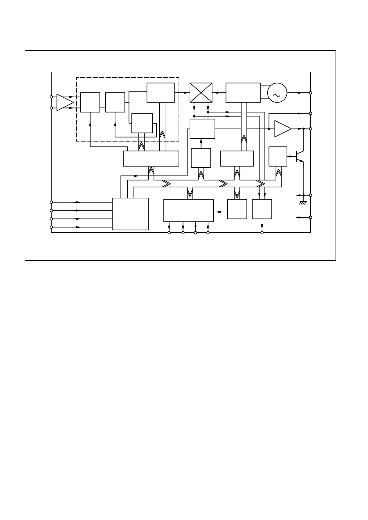
Fig. 2 SP5658S block diagram
2

SP5658
ELECTRICAL CHARACTERISTICS
T amb = –20°C to + 80°C, VCC = + 4.5V to + 5.5V. Reference frequency = 4MHz. These characteristics are guaranteed by
either production test or design. They apply within the specified ambient temperature and supply voltage ranges unless otherwise
stated.
Characteristics Pin Units Conditions
Value
(SP5658S)
Supply current, I
CC
12 59 74 mA V
RF input voltage 13, 14 40 300 mV
Min Typ Max
52 65 mA V
=5V Prescaler enabled, DE=1
CC
=5V Prescaler disabled, DE=0
CC
300MHz to 2.7GHz Prescaler
rms
enabled, DE=1, See Fig. 5b
13,14 100 300 mV
80MHz Prescaler enabled,
rms
DE=1, See Fig. 5b.
13, 14 40 300 mV
100MHz to 2.0GHz Prescaler
rms
disabled, DE=0, See Fig. 5a
13,14 50 300 mV
80MHz Prescaler disabled,
rms
DE=0, See Fig. 5a.
RF input impedance 13, 14 50 Ω Refer to Fig. 4
RF input capacitance 13, 14 2 pF Refer to Fig. 4
Data, Clock, Enable & Disable 3,4,5,6
Input high voltage 3 V
CC
V
Input low voltage 0 0.7 V
Input high current 10 µA Input voltage = V
Input low current –10 µA Input voltage = V
Clock Rate 6 500 kHz
Clock data & enable input 4,5,6 0.4 V
hysteresis
CC
EE
3

SP5658
ELECTRICAL CHARACTERISTICS
T amb = –20°C to + 80°C, VCC = + 4.5V to + 5.5V. Reference frequency = 4MHz. These characteristics are guaranteed
by either production test or design. They apply within the specified ambient temperature and supply voltage ranges unless
otherwise stated.
Characteristics Pin Value Units Conditions
(SP5658S)
Min Typ Max
Bus Timing 4,5,6
Data set up, t
Data hold, t
Enable set up, t
Enable hold, t
Clock to enable, t
SU
HD
ES
EH
CE
Charge pump output current 1 See Table 3, V
Charge pump output leakage 1 ± 3 ± 10 nA V
Charge pump drive output 16 1 mA V
current
300 ns See Fig. 3
600 ns See Fig. 3
300 ns See Fig. 3
600 ns See Fig. 3
300 ns See Fig. 3
= 2V
PIN1
= 0.7V
PIN16
PIN1
= 2V
Oscillator temperature stability 2 2 ppm/°C
Oscillator supply voltage 2 2 ppm/V
stability
External reference input 2 2 20 MHz AC coupled sinewave
frequency
External reference input 2 200 500 mV
amplitude
AC coupled sinewave
PP
Crystal frequency 2 4 12 MHz
Crystal oscillator drive level 2 45 mV
PP
Recommended crystal series 100 200 Ω Applies to 4MHz crystal only.
resistance ‘‘Parallel resonant” crystal. Figure
quoted is under all conditions
including start up.
Crystal oscillator negative 2 400 Ω Includes temperature and process
resistance tolerances.
Comparison frequency 2 MHz
Phase noise at phase detector –142 dBC/ 6kHz loop BW, phase comparator
Hz freq 250kHz. Figure measured @
1kHz offset, DSB (within loop band
width).
RF division ratio 240 131071 Prescaler disabled, DE=0
480 262142 Prescaler enabled, DE=1
Reference division ratio See Table 1
Output ports P0–P3 # 7,8,9,10
Sink current 10 mA V
Leakage current 10 µAV
PORT
PORT
=0.7V
=13.2V
Lock output 11
Sink current 1 mA V
=0.7V, ‘out of lock’
LOCK
Leakage current 10 µA ‘in lock’
4
# Ports P2 and P3 are not available on the SP5658F.

ABSOLUTE MAXIMUM RATINGS
All voltages are referred to V EE at 0V
Characteristics Pin Min Max Units Conditions
(SP5658S)
SP5658
Supply voltage, V
CC
RF input voltage 13, 14 2.5 V
12 –0.3 7 V
p–p
AC coupled as per application
RF input DC offset 13, 14 –0.3 VCC +0.3 V
Port voltage 7 – 10 –0.3 14 V Port in off state
7 – 10 –0.3 6 V Port in on state
Total port current 7 – 10 50 mA
Lock output DC offset 11 –0.3 V
Charge pump DC offset 1 –0.3 V
+0.3 V
CC
+0.3 V
CC
Drive DC offset 16 –0.3 VCC +0.3 V
Crystal DC offset 2 –0.3 VCC +0.3 V
Data, Clock, Enable & Disable DC 3 – 6 –0.3 V
+0.3 V
CC
offset
Storage temperature –55 +125 °C
Junction temperature 150 °C
MP14 Thermal Resistance
Chip to ambient 123 °C/W
Chip to case 45 °C/W
MP16 Thermal Resistance
Chip to ambient 111 °C/W
Chip to case 41 °C/W
Power consumption at V
=5.5V 407 mW All ports off, prescaler enabled
CC
ESD protection ALL 2 kV MIL–STD 883 TM 3015
FUNCTIONAL DESCRIPTION
The SP5658 contains all the elements necessary, with the
exception of a frequency reference, loop filter and external
high voltage transistor, to control a varicap tuned local
oscillator, so forming a complete PLL frequency synthesised
source. The device allows for operation with a high
comparison frequency and is fabricated in high speed logic,
which enables the generation of a loop with good phase noise
performance. The RF preamplifier contains a selectable
divide by two for operation above 2.0GHz. Up to 2GHz the RF
input interfaces directly with the programmable divider, so
eliminating degradation in phase noise due to the prescaler
action. The block diagram is shown in Fig.2.
The SP5658 is controlled by a standard 3–wire bus
comprising data, clock and enable inputs. The programming
word for the 16 pin variant contains 28 bits, four of which are
used for port selection, 18 to set the programmable divider
ratio and enable/disable the prescaler, bit DE, three bits to
select the reference division ratio, bits R0–R2, one bit to set
charge pump current, bit C0, and the remaining two bits to
access test modes, bit T0, and to disable the varactor drive,
bit OS. The data word for 14 pin variant is identical to 16 pin
except 26 bits only are required, two of which are used for port
selection. The programming format is shown in Fig. 3.
The clock input is disabled by an enable low signal, data
is therefore only clocked into the internal shift registers during
an enable high and is loaded into the controlling buffers by an
enable high to low transition. This load is also synchronised
with the programmable divider so giving smooth fine tuning.
The RF signal is fed to an internal preamplifier, which
provides gain and reverse isolation from the divider signals.
The output of the preamplifier is fed to the 2/1 selectable
prescaler and then to the 17 bit fully programmable divider,
which is of MN+A architecture. The M counter is 13 bit and the
A counter 4. If bit DE is set to a 0 the prescaler is disabled; Note
that the control function DE cannot be used dynamically.
The output of the programmable divider is fed to the phase
comparator where it is compared in both phase and frequency
domain with the comparison frequency. This frequency is
derived either from the on board crystal controlled oscillator or
from an external source. In both cases the reference
frequency is divided down to the comparison frequency by the
reference divider which is programmable into 1 of 8 ratios as
described in Table 1.
The output of the phase comparator feeds the charge
pump and loop amplifier section, which when used with an
external high voltage transistor and loop filter integrates the
current pulses into the varactor line voltage. The charge pump
can be disabled to a high impedance state by the DISABLE
input. The varactor drive output can also be disabled by the OS
bit within the data word, so switching the external transistor
‘OFF’ and allowing an external voltage to be written to the
varactor line for tuner alignment purposes.
The phase comparator also drives the lock detect circuit
which generates a lock flag. ‘In–lock’ is indicated by a high
impedance state on the lock output.
The programmable divider output divided by 2, F pd /2 and
the comparison frequency, F comp can be switched to ports P0
and P1 respectively by switching the device into test mode.
The test modes are described in Table 2.
5
 Loading...