MITEL SP5512KGMPAS Datasheet

The SP5512 is a single-chip frequency synthesiser designed
for TV tuning systems. Control data is entered in the standard
I2C BUS format. The device has six controllable open-collector
output ports (P2-P7), each capable of sinking 20mA. In addition,
P6 is a 3-bit 5-level ADC input. The information on these ports
can be read via the I2C BUS.
The device has one fixed I2C BUS address and three
programmable addresses, allowing two or more synthesisers
to be used in a system.
FEATURES
■ Complete 1·3GHz Single Chip System
■ Programmable via the I
2
C BUS
■ Low Power Consumption (215mW Typ.)
■ Low Radiation
■ Phase Lock Detector
■ Varactor Drive Amp Disable
■ 6 Controllable Outputs, 5 Bi-directional
■ 5-Level ADC
■ Variable I
2
C BUS Address for Picture in Picture TV
■ ESD Protection *
* Normal ESD handling precautions should be observed.
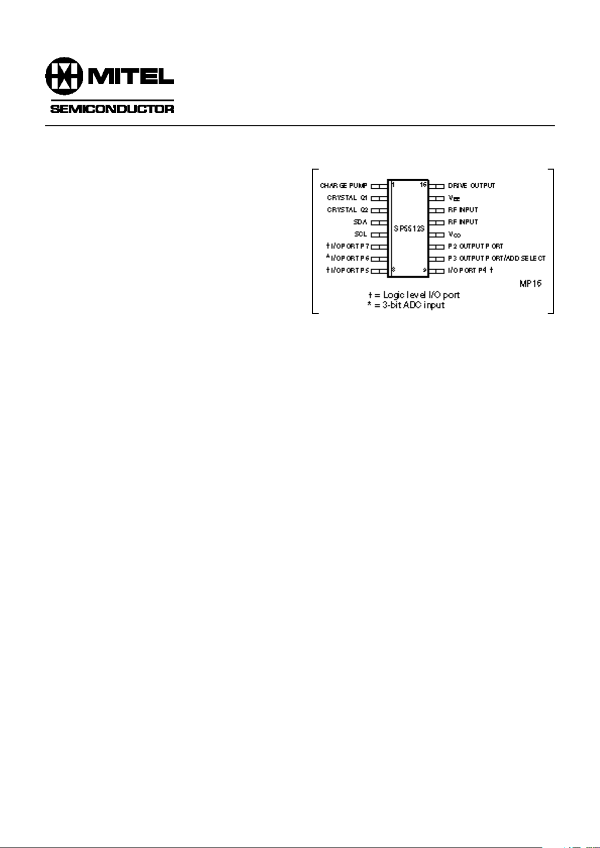
Fig. 1 Pin connections – top view
APPLICATIONS
■ Cable Tuning Systems
■ VCRs
ORDERING INFORMATION
SP5512S KG MPAS (16-lead miniature plastic package)
SP5512
1.3GHz Bidirectional I2C BUS Controlled Synthesiser
Supersedes version in April 1994 Consumer IC Handbook, HB3120 - 2.0 DS2384 - 4.0 January 1997

2
SP5512
ELECTRICAL CHARACTERISTICS
T
AMB
= 210°C to 180°C, VCC = 14·5V to 15·5V.
These Characteristics are guaranteed by either production test or design. They apply within the specified ambient temperature
and supply voltage ranges unless otherwise stated. Reference frequency 4MHz unless otherwise stated.
Supply current
Prescaler input voltage
Prescaler input impedance
Prescaler input capacitance
SDA, SCL
Input high voltage
Input low voltage
Input high current
Input low current
Leakage current
SDA
Output voltage
Charge pump current low
Charge pump current high
Charge pump output leakage current
Charge pump drive output current
Charge pump amplifier gain
Recommended crystal series resistance
Crystal oscillator drive level
Crystal oscillator negative resistance
Output Ports
P2-P7 sink current (see note 1)
P2-P7 leakage current (see note 1)
Input Ports
P3 input current high
P3 input current low
P4, P5, P7 input voltage low
P4, P5, P7 input voltage high
P6 input current high
P6 input current low
Typ.
Value
Conditions
Characteristic Pin
12
13,14
13,14
4,5
4,5
4,5
4,5
4,5
4
1
1
1
16
2
6-11
6-11
10
10
6,8,9
6,8,9
7
7
12·5
30
3
0
500
10
750
20
2·7
43
50
2
650
6170
6400
40
53
300
300
5·5
1·5
10
210
10
0·4
65
200
10
110
210
0·8
110
210
Units
Min. Max.
mA
mVrms
mVrms
Ω
pF
V
V
µA
µA
µA
V
µA
µA
nA
Ω
mV p-p
Ω
mA
µA
µA
µA
V
V
µA
µA
VCC = 5V
50MHz to 1GHz
1·3GHz, see Fig. 5
Input voltage = V
CC
Input voltage = 0V
When VCC = 0V
Sink current = 3mA
Byte 4, bit 2 = 0, pin 1 = 2V
Byte 4, bit 2 = 1, pin 1 = 2V
Byte 4, bit 4 = 1, pin 1 = 2V
V pin 16 = 0·7V
Parallel resonant crystal (note 2)
V
OUT
= 0·7V, see note 1
V
OUT
= 13·2V
V pin 10 = 13·2V
V pin 10 = 0V
See Table 3 for ADC levels
NOTES
1. Source impedance between all output ports and ground is approximately 5Ω . This should be taken into account when calculating output port
saturation voltages.
2. The recommended crystal series resistance quoted refers to all conditions including start-up.

3
SP5512
ABSOLUTE MAXIMUM RATINGS
All voltages are referred to VEE and pin 3 at 0V.
Supply voltage
RF input voltage
Port voltage
Total port output current
RF input DC offset
Charge pump DC offset
Drive output DC offset
Crystal oscillator DC offset
SDA, SCL input voltage
Storage temperature
Junction temperature
MP16 thermal resistance, chip-to-ambient
MP16 thermal resistance, chip-to-case
Power consumption at 5·5V
Conditions
Parameter
12
13,14
6-11
6-11
6-11
13-14
1
16
2
4,5
Pin
Max.Min.
Units
Value
20·3
20·3
20·3
20·3
20·3
20·3
20·3
20·3
20·3
255
V
V p-p
V
V
mA
V
V
V
V
V
V
°C
°C
°C/W
°C/W
mW
Port in off state
Port in on state
With VCC applied
V
CC
not applied
7
2·5
14
6
50
VCC10·3
VCC10·3
VCC10·3
VCC10·3
VCC10·3
5·5
1150
1150
111
41
321
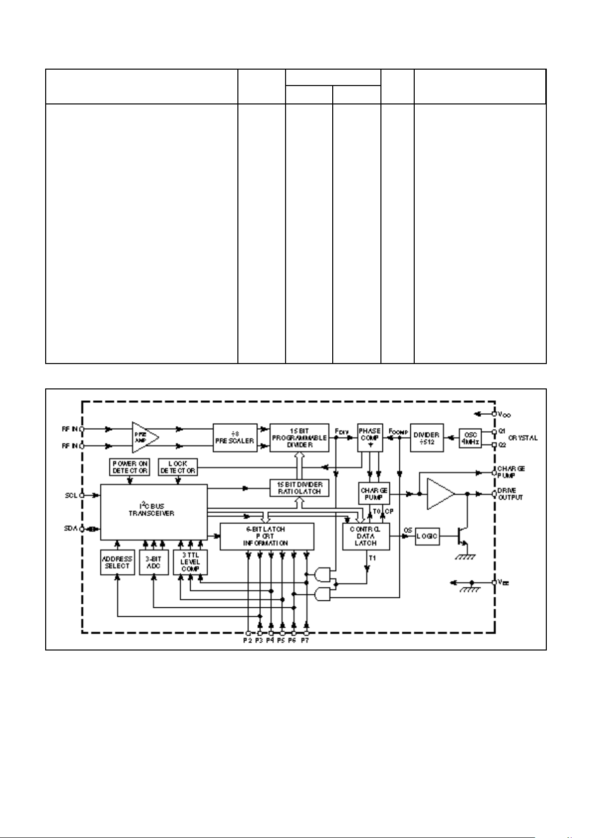
Fig. 2 Block diagram
 Loading...