MITEL SL6140MP, SL6140MPTC, SL6140NA Datasheet

Features
● 400MHz Bandwidth (R
● High voltage Gain 45dB (R
● 70dB Gain Control Range
● High Output Level at Low Gain
● Surface Mount Plastic Package
● Low Cost
=50Ω)
L
=1kΩ)
L
Applications
● RF/IF Amplifier
● High Gain Mixers
● Video Amplifiers
Description
The SL6140 is an integrated broadband AGC amplifier,
designed on an advanced bipolar process. The
amplifier provides over 15dB of linear gain into 50Ω at
400MHz. Gain control is also provided with over 70dB
of dynamic range. The SL6140 offers over 45dB of
voltage gain with an RL of 1kΩ.
SL6140
SL6140
400MHz Wideband AGC Amplifier
DS2159 Issue no 5.0 July 1999
Ordering Information
SL6140/NA/MP Industrial temperature range
SL6140/NA/MPTC Tape and Reel
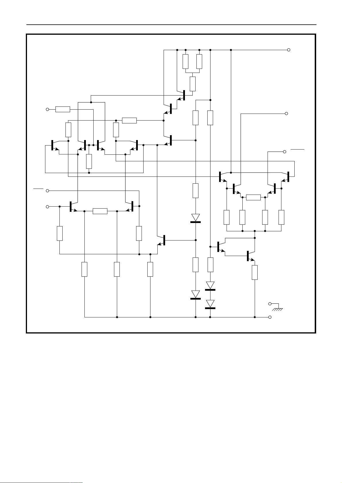
The SL6140 (Figure 3) is a high gain amplifier with an
AGC control capable of reducing the gain of the amplifier
by over 70dB. The gain is adjustable by applying a
voltage to the AGC input via an external resistor (R
the value of which adjusts the curve of gain reduction
versus control voltage (see Figure 4). As the output
stage of the amplifier is an open collector the maximum
voltage gain is determined by RL. With load resistance
of 1kΩ the single ended voltage gain is 45dB and with a
load resistance of 50Ω the voltage gain is 15dB (20log
V
OUT/VIN
). Another parameter that depends on the load
resistance is the bandwidth: 25MHz for RL = 1kΩ, as
compared with 400MHz for RL = 50Ω. RL is chosen to
give either the required bandwidth or voltage gain for the
circuit.
Figure 7 through to 10 show the typical S parameters for
the device. Figures 11 and 12 show the typical variation
in 3rd order intercept performance with AGC.
In any application, the substrate should be connected to
the most negative point in the circuit, usually to the same
point as pin 3.
miniature plastic package
AGC
10
),
AGC
INPUT
INPUT
R
AGC
10n
10n
+VCC
1.0 F
2
6
5
SL6140
4
37
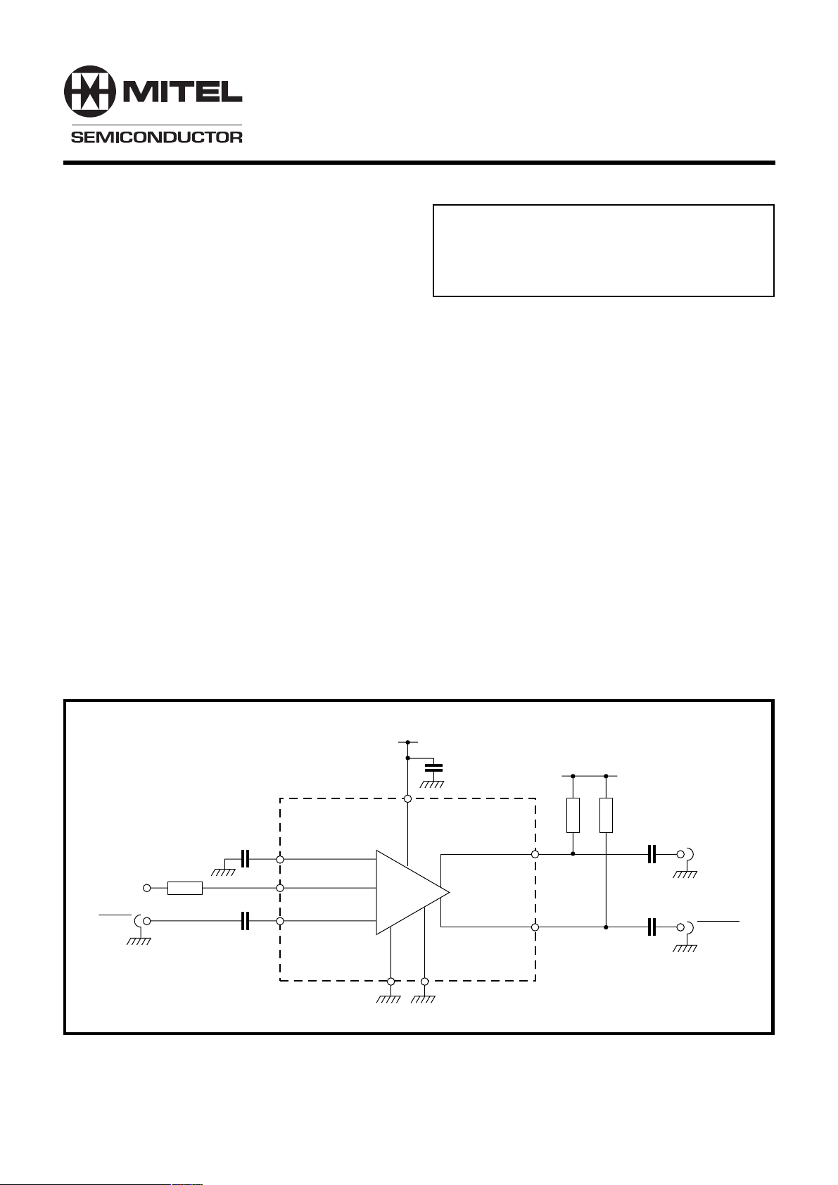
Figure 1 Typical Application
8
1
RLR
+VCC
L
10n
OUTPUT
10n
OUTPUT
1

SL6140
OUTPUT
+V
CC
GROUND INPUT
INPUT
18
27
36
45
OUTPUT
GROUND
AGC INPUT
MP8
Figure 2 Pin Connections Diagram (top view)
Electrical Characteristics
T
= 25°C, VCC = 12V +5%, VIN = 1mV
amb
These characteristics are guaranteed over the following conditions (unless otherwise stated)
Characteristic
Supply current
Output stage current
Output current matching
(magnitude of difference of output
currents)
Pin
5,6,7
5,6
(sum)
5,6
, Frequency = 6MHz, Load (RL) = 10KOHms, R
RMS
Value
TypMin
19
5
7
1.0
Max
23
9
Units
mA
mA
mA
No input signal
No input signal
Conditions
= 22KOHm
AGC
AGC range
Voltage gain (single ended)
Bandwidth (-3dB)
Maximum output level (single
ended)
0dB AGC
-30dB AGC
Noise figure
Note. 1 Guaranteed but not tested.
2
5,6
5,6
5,6
5,6
5,6
5,6
60
40
Absolute Maximum Ratings
Supply voltage, V
Input voltage (differential) +5V
AGC supply V
Storage temperature -55°C to +150°C
Operating temperature range
SL6140 MP -40°C to +85°C
Chip operating temperature
SL6140 MP +150°C
CC
at 200mW
+18V
CC
75
45
55
15
25
400
3.5
3.5
5
Thermal Resistance
Chip-to-ambient
SL6140 MP 163°C/W
Chip-to-case
SL6140 MP 57°C/W
dB
dB
dB
dB
MHz
V p-p
V p-p
dB
See Figure 4 & Note 1
(VAGC = 0V to 10V)
R
= 1kΩ See Figure 5 & Note 1
L
Tuned input and output
R
= 50Ω
L
RL = 1kΩ See Figure 5
RL = 50Ω
Note 1
R
= 1kΩ. Note 1
L
Test CCT Figure 13
2

180
470
X 2
SL6140
2
V
CC
AGC
INPUT
INPUT
70
5
I/P
2k
4
6
66
180
470470
5k5k
2.1k1.1k1.1k
7k 12.1k
1.4k
5.6k
1.9k
45
2.8k 2.8k200 200
200
1
8
OUTPUT
OUTPUT
Figure 3 Full Circuit Diagram of SL6140
7
3
SUBSTRATE
GROUND
3
 Loading...