MITEL SL1925KG, SL1925NP2S, SL1925NP2T, SL1925 Datasheet

SL1925
Satellite Zero IF QPSK Tuner IC
Preliminary Information
Description
The SL1925 is a wideband quadrature converter operating
from 950 to 2150 MHz, intended primarily for application
in satellite tuners.
The device contains all elements necessary, with the
exception of local oscillator sustaining network, to fabricate
a high performance I(n-phase) & Q(uadrature) phase
splitter and downconverter optimised for systems
containing RF AGC gain control. The device allows for
systems containing higher power analog interferers. For
most applications RF tunable filtering is not essential.
The SL1925 is optimised for use with a low phase noise
synthesiser, a range of which are available from Mitel
Semiconductor. This will form a complete front end tuner
function for digital satellite receiver systems utilising DSP
derotation recovery.
The device includes a very high signal handling front end
with AGC, this provides for gain control, reference local
oscillator with output buffer, phase splitter with I and Q
mixers and baseband buffer amplifiers with external
interstage filtering.
Features
● Single chip system for direct quadrature down
conversion from L-band
● High signal handling capability for minimum
external component count application, requires
external RF AGC of 30dB
● Compatible with DSS and DVB system
requirements
● Excellent gain and phase match up to 30MHz
baseband
● High output referred linearity for low distortion and
multi channel application
● Fully balanced low radiation design
● Integral RF AGC amplifier
● Two selectable varactor tuned local oscillators
with buffered output for driving external
synthesiser loop
● ESD protection (Normal ESD handling procedures
should be observed)
Ordering Information
SL1925/KG/NP2S (Tubes)
SL1925/KG/NP2T (Tape and Reel)
Applications
● Satellite receiver systems
● Data communications systems
DS4955 Issue - 2.0 March 1999
2
SL1925 Preliminary Information
NP28
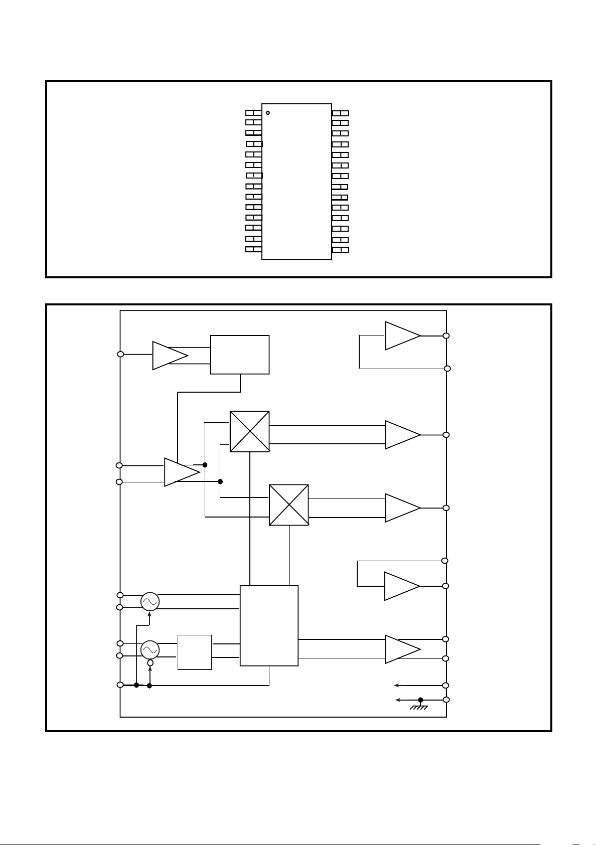
Figure 1 Pin connections
OPFI
OPFQ
Vcc
PSout
PSoutb
Vee
Tanks
Tanksb
Vee
Tankv
Tankvb
Vee
NC
Vcc
128
14
15
Vee
IPFI
Vee
Iout
LOsel
Vcc
RF
RFB
Vee
AGC
Qout
Vee
IPFQ
Vee
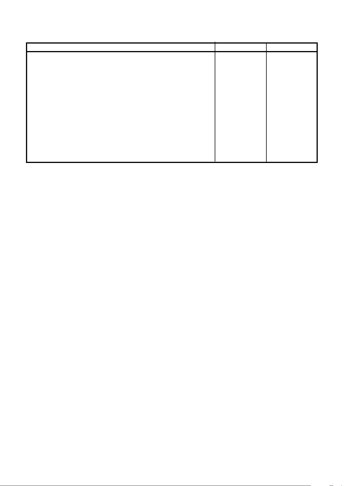
Figure 2 Block diagram
27
AGC
19
22
21
RF
RFB
9
10
Tankv
Tankvb
6
7
24
Tanks
Tanksb
LOsel
vcos
DIVIDE
BY 2
AGC
SENDER
0 DEG
25
Iout
IPFI
1
OPFI
14
OPFQ
16
IPFQ
18
Qout
3
PSout
4
PSoutb
2, 13, 23 Vcc
5, 8, 11, 15, 17, 20, 26, 28
Vee
90 DEG
vcov
FREQUENCY
AGILE
PHASE
SPLITTER
3
Preliminary Information SL1925
Quick Reference Data
Characteristic Units
Operating range 950-2150 MHz
Input noise figure, DSB, maximum gain, 1500MHz 19 dB
Maximum conversion gain (assuming 6dB filter loss) >55 dB
Minimum conversion gain (assuming 6dB filter loss) <20 dB
IP32T input referred 113 dBuV
Converter input referred IM3, two tones at 97dBµV 30 dBc
IP22T input referred 140 dBuV
P1dB input referred 103 dBuV
Baseband amplifier Output limit voltage 2.0 V
Gain match up to 22 MHz 0.2 dB
Phase match up to 22 MHz 0.7 deg
Gain flatness up to 22 MHz 0.5 dB
Local oscillator phase noise across entire 950MHz to 2150MHz band:
SSB @ 10 kHz offset 80 dBc/Hz
Table 1
The required 950MHz to 2150MHz I and Q reference LO
frequencies for quadrature direct conversion are
generated by the on board oscillators named ‘vcos’ and
‘vcov’, and the phase splitter. Oscillator ‘vcos’ operates
nominally from 1900MHz to 3000MHz and is then divided
by two to provide 950MHz to 1500MHz. Oscillator ‘vcov’
operates nominally from 1400MHz to 2150MHz. Only
one oscillator is active at any time and selection is made
within the phase splitter under the control of the LOsel
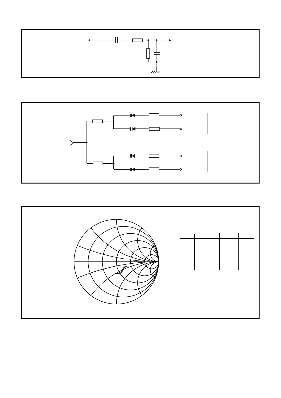
input. Each oscillator uses an external varactor tuned
resonant network optimised for low phase noise with a
single varactor line control. A recommended application
circuit for the oscillators is shown in Figure 4. The LO
from the phase splitter drives a buffer whose outputs
‘PSout’ and ‘PSoutb’ can be used for driving an external
PLL control loop for the VCO’s. The typical LO phase
noise is shown in Figure 11.
The mixer outputs are coupled to baseband buffer
outputs ‘OPFI’ and ‘OPFQ’ which drive external band
limit filters. The output impedance of these buffers is
contained in Figure 12. The outputs of the filters are then
connected to the inputs ‘IPFI’ and ‘IPFQ’ of the baseband
channel amplifiers. The outputs ‘Iout’ and ‘Qout’ provide
for a low impedance drive and can be used with a
maximum load as in Figure 3. The output impedance of
this section is contained in Figure 13. An example filter
for application with 30MS/s systems is contained in
Figure 14.
All port peripheral circuitry for the SL1925 is shown in
Figure 15a and 15b.
The typical key performance data at 5V Vcc and 25°C
ambient are shown in the ‘QUICK REFERENCE DATA’
of Table 1.
Functional Description
The SL1925 is a wideband direct conversion quadrature
downconverter optimised for application in satellite
receiver systems. A block diagram is given in Figure 2
and shows the device to include a broadband RF
preamplifier with AGC control, two oscillator sustaining
amplifiers, a frequency agile 90° phase splitter, I Q
channel mixers and I Q channel baseband amplifiers.
The only additional elements required are an external
tank circuit for each oscillator, and baseband interstage
filters. To fabricate a complete tuner an RF AGC stage
offering +20dB to -10 dB of gain range and a 2.2 GHz
PLL frequency synthesiser are also required. An example
application is shown in Figure 16.
In normal application the first satellite IF frequency of
typically 950 to 2150 MHz is fed via the tuner RF AGC
stage to the RF preamplifier, which is optimised for
impedance match and signal handling. The RF
preamplifier is designed such that no tracking RF filter is
required and also allows for analog interferers at up to
10 dB higher amplitude. The converter RF input
impedance is shown in Figure 5. The amplifier signal is
then fed to an AGC stage providing a minimum of 35dB
AGC control, which together with the RF attenuator
provides a possible overall tuner dynamic range of
65dB, to allow for normal operating dynamic range and
MCPC systems. The signal is then split into two balanced
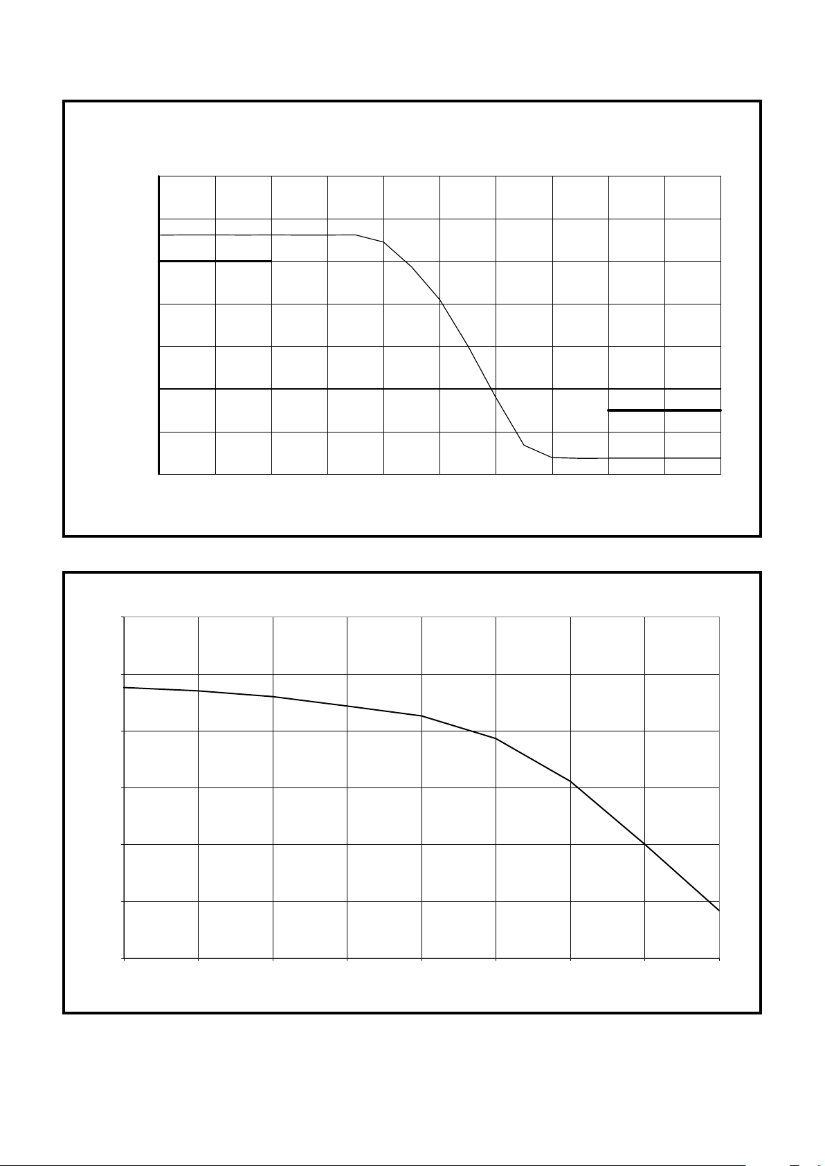
channels to drive the I and Q mixers. The AGC
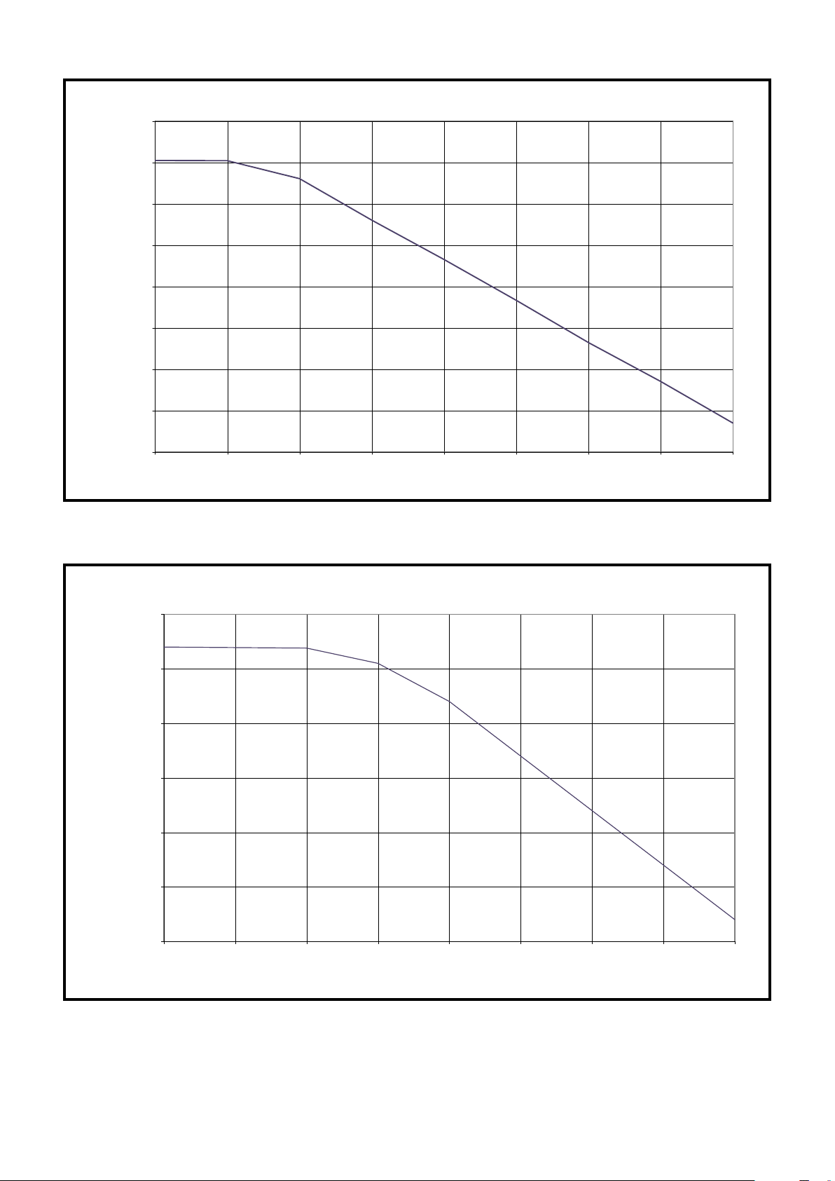
characteristic, and gain variation of IIP3, IIP2, P1dB and
NF are contained in Figs. 6, 7, 8, 9 and 10 respectively.
4
SL1925 Preliminary Information
Figure 3 Baseband output load condition
15pF
100Ω
1kΩ
Note: Stripline width =0.44mm,dimensions are approximate.
Marker Freq (MHz) Zreal Ω Zimag Ω
1 950 90 -18
2 1350 76 -15
3 1750 63 -35
4 2150 46 -29
Figure 5 Converter RF input impedance (typical)
0.50.2 10
+j0.2
+j0.5
+j1
+j2
+j5
2 5
–j5
–j2
–j1
–j0.5
–j0.2
STOP 2 500
START 700
X
X
X
X
X
1
2
3
4
Normalised to 50Ω
MHz
MHz
Figure 4 Local oscillator application circuit
"vcov"
1T379
1T379
BB811
BB811
1kΩ
Vcnt
6.15MM STRIPLINE
6.15MM STRIPLINE
9MM STRIPLINE
9MM STRIPLINE
6
7
9
10
Tanks
Tanksb
Tankv
Tankvb
"vcos"
1kΩ
5
Preliminary Information SL1925
Figure 6 Converter gain variation with AGC voltage (typical)
-20.0
-10.0
0.0
10.0
20.0
30.0
40.0
50.0
0.0 0.5 1.0 1.5 2.0 2.5 3.0 3.5 4.0 4.5 5.0
AGC control voltage (V)
Converter conversion gain (dB)
30dB minimum, AGC <1V
-5dB maximum, AGC >4V
90
95
100
105
110
115
120
-6 -1 4 9 14 19 24 29 34
Converter gain setting (dB)
Converter input referred IP3 (dBuV)
Figure 7 Converter input referred IP3 variation with gain setting (typical)
6
SL1925 Preliminary Information
100
105
110
115
120
125
130
135
140
-6 -1 4 9 14 19 24 29 34
Converter gain setting (dB)
Converter input referred IP2 (dBuV)
Figure 8 Converter input referred IP2 variation with gain setting (typical)
80
85
90
95
100
105
110
-6 -1 4 9 14 19 24 29 34
Converter gain setting (dB)
Converter RF input level at P1dB (dBuV)
Figure 9 Converter input referred 1dB gain compression, P1dB (typical)
 Loading...