MITEL SL1461KG, SL1461MPAS, SL1461SA Datasheet

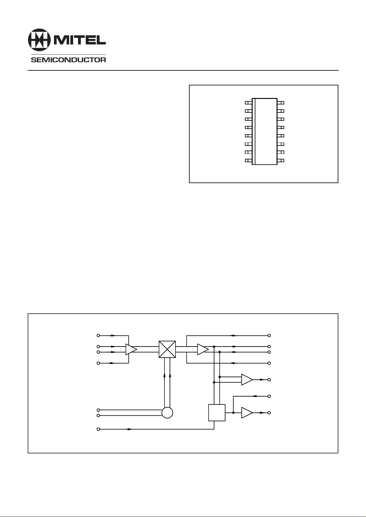
The SL1461SA is a wideband PLL FM demodulator,
intended primarily for application in satellite tuners.
The device contains all elements necessary, with the
exception of external oscillator sustaining network and loop
feedback components, to form a complete PLL system
operating at frequencies up to 800MHz.
An AFC with window adjust is provided, whose output
signal can be used to correct for any frequency drift at the head
end local oscillator.
FEATURES
■ Single chip PLL system for wideband FM
demodulation
■ Simple low component count application
■ Allows for application of threshold extension
■ Fully balanced low radiation design
■ High operating input sensivity
■ Improved VCO stability with variations in supply or
temperature
■ AGC detect and bias adjust
■ 75Ω video output drive with low distortion levels
■ Dynamic self biasing analog AFC
■ Full ESD Protection*
* Normal ESD handling procedures should be observed
Wideband PLL FM Demodulator
Advance Information
DS4049 - 1.2 December 1994
AFC PUMP
AFC WINDOW ADJUST
EE
V
OSCILLATOR +
OSCILLATOR –
AGC BIAS
AGC OUTPUT
RF INPUT
Fig.1 Pin connections - top view
APPLICATIONS
■ Satellite receiver systems
■ Data communications Systems
ORDERING INFORMATION
SL1461SA/KG/MPAS
16116
2
15
3
14
4
13
5
12
SL1461SA
6
11
10
7
89
SL1461SA
AFC OUTPUT
V
CC
VIDEO FEEDBACK +
VIDEO –
VIDEO +
VIDEO FEEDBACK –
VIDEO OUTPUT
RF INPUT
MP16
AGC BIAS
RF INPUTS
AGC OUTPUT
LOCAL
OSCILLATOR
AFC WINDOW
ADJUST
6
8
9
7
4
5
2
14
VIDEO
FEEDBACK +
12
VIDEO +
13
VIDEO –
11
VIDEO
FEEDBACK –
10
VIDEO
OUTPUT
1
AFC PUMP
16
AFC OUTPUT
Fig.2 SL1461SA block diagram

SL1461SA
ELECTRICAL CHARACTERISTICS
T
= -20°C to +80°C, VCC = +4.5V to +5.5V. The electrical characteristics are guaranteed by either production test or design.
amb
They apply within the specified ambient temperature and supply voltage unless otherwise stated.
Characteristics
Supply current
Operating frequency
Input sensitivity
Input overload
VCO sensitivity (dF/dV)
VCO linearity
VCO supply stability
VCO temperature stability
Phase detector gain
Loop amplifier input impedance
Loop amplifier output impedance
Loop amplifier open loop gain
Loop amplifier gain bandwidth product
Loop amplifier output swing
Video drive output impedance
Video drive:
Luminance nonlinearity
- differential gain
- differential phase
- intermodulation
- signal/noise
- Tilt
- baseline distortion
AGC output current
AGC bias current
AFC window current
AFC charge pump current
AFC leakage current
AFC output saturation voltage
Value
Min. Typ. Max.
36
300
40
800
-40
0
25
32
39
25
2.0
20
0.5
0.25
450
570
700
25
38
240
1.2
55
75
1.9
0.5
1.0
95
5
2.5
3
-40
66
10
0
0
72
0.3
0.4
3
2
400
250
400
50
10
0.4
Units
mA
MHz
dBm
dBm
MHz/V
%
MHz/V
KHz/°C
V/rad
V/rad
Ω
Ω
dB
MHz
Vp-p
Ω
%
%
Degree
dB
dB
%
%
µA
µA
µA
µA
µA
V
Conditions
Preamp limiting
Refer to application in Fig. 3
Refer to application in Fig. 3; with
13.5MHz p-p deviation
See note 5
See note 5
Differential loop filter
Single ended loop filter
Single ended
Single ended
Single ended
Single ended
Single ended
1KΩ load, See note 3 and 4
75KΩ load, See note 3 and 4
75KΩ load, See note 3 and 4
See notes 1, 3 and 4
1KΩ load, See note 2 and 4
1KΩ load, See note 3 and 4
1KΩ load, See note 3 and 4
Maximum load voltage drop 2V
400µA gives 1.5V deadband window
With charge pump disabled
AFC output enabled
Note 1. Product of input modulation f 1 at 4.43MHz, 13.5MHz p–p deviation and f 2 at 6MHz p–p deviation, (PAL chroma and sound
subcarriers).
Note 2. Ratio of output video signal with input modulation at 1MHz, 13.5MHz p–p deviation, to output rms noise in 6MHz bandwidth with
no input modulation.
Note 3. Input test signal pre–emphasised video 13.5MHz p–p deviation. Output voltage 600mV pk–pk.
Note 4. See page 3
Note 5. Assuming operating frequency of 479.5MHz set with V
shown in Fig. 3. also refer to Fig. 8.
@ 5.0V and ambient temperature of +20°C. Only applies to Application
CC
2

SL1461SA
TEST CONFIGURATION
VIDEO GENERATOR
ROHDE & SCHWARZ SGPF
PRE EMPHASISED BASE BAND VIDEO
DE EMPHASISED BASE BAND VIDEO 1V p–p
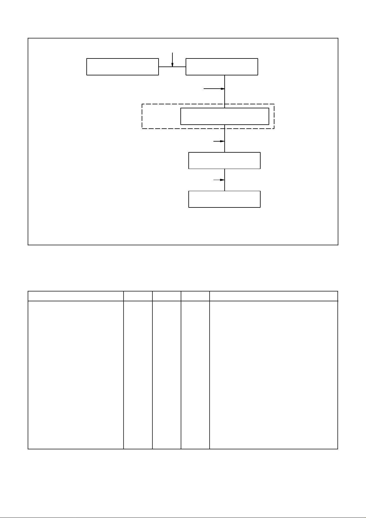
The video drive characteristics measurements were made using the above test configuration. The maximum figures recorded in
the Electrical Characteristics Table coincide with high temperatures and extremes of supply voltage. No adjustment to the recorded
figures has been made to compensate for the effects of temperature on the external components of the application test board, in
particular the varactor diodes. If operation of the device at high ambient temperatures is envisaged then attention to temperature
compensation of the external circuitry will result in performance figures closer to the stated typical figures.
BASE BAND VIDEO 1V p–p
ROHDE & SCHWARZ SFZ
RF CARRIER FREQ 479.5MHz
FM MODULATION 13.5MHz P–P
PRE–EMPHASISED VIDEO
MONTFORD
TEST OVEN
SL1461 TEST APPLICATION BOARD
See Fig. 3 for details
DE EMPHASISED NETWORK
ROHDE & SCHWARZ UAF
TV SAT TEST TX
VIDEO AMPLIFIER/
VIDEO ANAL YSER
ABSOLUTE MAXIMUM RATINGS
All voltages are referred to VEE at 0V
Characteristics
Supply voltage
RF input voltage
RF input DC offset
Oscillator ± DC offset
Video ± DC offset
Video feedback ± DC offset
Video output DC offset
AFC pump DC offset
AFC disable DC offset
AFC deadband DC offset
AGC bias DC offset
AGC output DC offset
Storage temperature
Junction temperature
MP16 package thermal resistance,
chip to ambient
Fig.2 SL1461SA block diagram
Min. Typ. Max.
-0.3
-0.3
-0.3
-0.3
-0.3
-0.3
-0.3
-0.3
-0.3
-0.3
-0.3
-55
7
2.5
V
+0.3
CC
V
+0.3
CC
V
+0.3
CC
VCC+0.3
V
+0.3
CC
V
+0.3
CC
V
+0.3
CC
VCC+0.3
V
+0.3
CC
V
+0.3
CC
125
150
111
V
Vp-p
V
V
V
V
V
V
V
V
V
V
°C
°C
°C/W
Conditions
3

SL1461SA
ABSOLUTE MAXIMUM RATINGS cont.
All voltages are referred to V
Characteristics
EE
at 0V
Min. Typ. Max.
Conditions
MP16 package thermal resistance,
chip to case
Power consumption at 5.5V
ESD protection - pins 1 to 15
ESD protection - Pin 16
2K
AGC BIAS AFC WINDOW ADJUST
RV1 RV2
D1
BB515
BB515
D2
C5
470nF
TP3
4n7
C6
2
1.7
50K
47nF 100nF
R1
4K7
R2
5K1
R3
4K7
41
250
1nF
°C/W
mW
kV
kV
27K
C2C1
16116
2
15
3
14
4
13
5
12
SL1461SA
6
11
10
7
89
C8C7
Mil-std-883 method 3015 class 1
Mil-std-883 method 3015 class 1
R6
R5
1K2
R4
1K2
1nF
TP4
C9
100pF
47
100nF
C11
C10
F
C3
TP1
TP2
100pF
F
47
C4
VIDEO OUTPUT
+5V
1nF
C12
RF INPUT
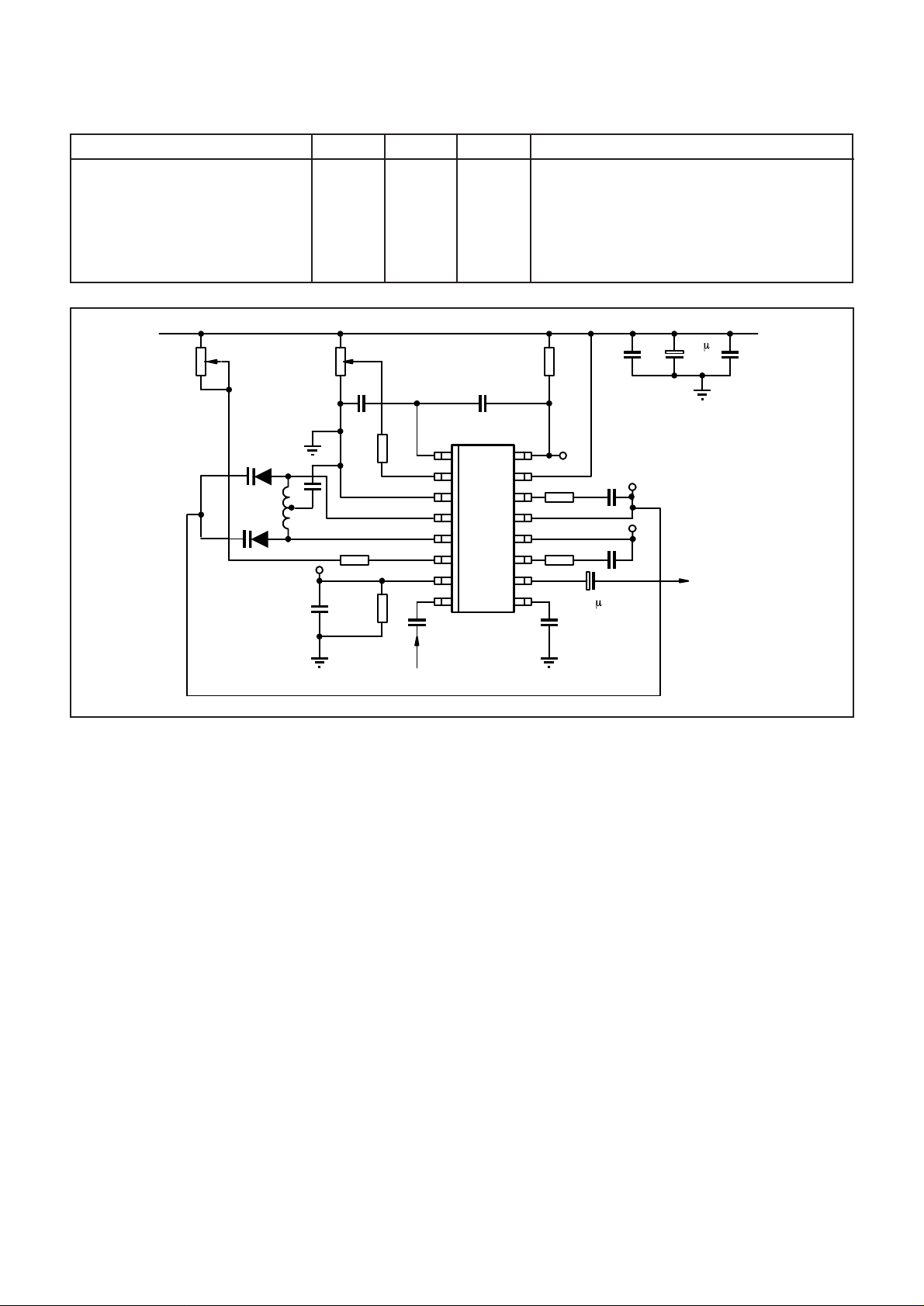
Fig.3 Standard application circuit
FUNCTIONAL DESCRIPTION
The SL1461SA is a wideband PLL FM demodulator,
optimised for application in satellite receiver systems and
requiring a minimum external component count. It contains all
the elements required for construction of a phase locked loop
circuit, with the exception of tuning components for the local
oscillator, and an AFC detector circuit for generation of error
signal to correct for any frequency drift in the outdoor unit local
oscillator. A block diagram is contained in Fig. 2 and the typical
application in Fig. 3.
The internal pin connections are contained in Fig.6/6a
In normal applications the second satellite IF frequency of
typically 402 or 479.5MHz is fed to the RF preamplifier, which
has a working sensitivity of typically -40 dBm, depending on
application and layout. The preamplifier contains an RF level
detect circuit, which generates an AGC signal that can be used
for controlling the gain of the IF amplifier stages, so maintaining
a fixed level to the RF input of the SL1461SA, for optimum
threshold performance. The bias point of the AGC circuit can
be adjusted to cater for variation in AGC line voltage
requirement and device input power. The typical AGC curves
are shown in Fig. 9. It is recommended that the device is
operated with an input signal between -30 and -35dBm. This
ensures optimum linearity and threshold performance, and
gives a good safety margin over the typical sensitivity of
-40dBm.
The output of the preamplifier is fed to the mixer section
which is of balanced design for low radiation. In this stage the
RF signal is mixed with the local oscillator frequency, which is
generatedby an on–board oscillator. The oscillator block uses
an external varactor tuned sustaining network and is optimised
for high linearity over the normal deviation range. A typical
frequency versus voltage characteristic for the oscillator is
contained in Fig. 7. The loop output is designed to compensate
for first order temperature variation effects; the typical stability
is shown in Fig. 8
The output of the mixer is then fed to the loop amplifier
around which feedback is applied to determine loop transfer
characteristic . Feedback can be applied either in differential or
single ended mode; if the appropriate phase detector gains are
assumed in calculating loop filters, both modes should give the
same loop response.
The loop amplifier drives a 75Ω output impedance buffer
amplifier, which can either be connected to a 75Ω load or used
to drive a high input impedance stage giving greater linearity
and approximately 6dB higher demodulated signal output
level.
4
 Loading...