

Datasheet PDSP16330, PDSP16330A, PDSP16330AAOAC, PDSP16330AC, PDSP16330ACOAC Datasheet (MITEL)
...Page 1
PDSP16330/A/B
Pythagoras Processor
Supersedes version September 1996, DS3884 - 1.3 DS3884 - 2.1 November 1998
The PDSP16330 is a high speed digital CMOS IC that
converts Cartesian data (Real and Imaginary) into Polar form
(Magnitude and Phase), at rates up to 20MHz. Cartesian
16+16 bit 2's complement or Sign-Magnitude data is
converted into 16 bit Phase format. The Magnitude output may
be scaled in amplitude by powers of 2. The Phase output
represents a full 2 x π field to eliminate phase ambiguities.
Polyimide is used as an inter-layer dielectric and as
glassivation.
The PDSP16330 is offered in three speed grades: a
basic 10MHz part (PDSP16330), a 20MHz version
(PDSP16330A) and a 25MHz version (PDSP16330). A MILSTD-883 version is also detailed in a separate datasheet.
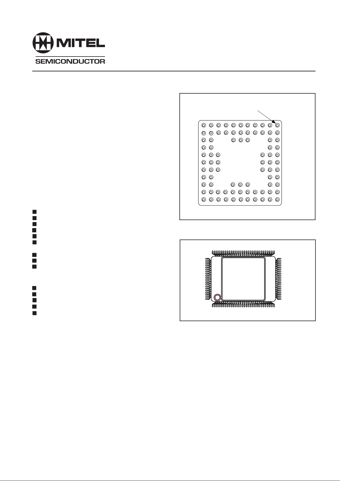
Fig.1 Pin connections - bottom view (PGA)
AC84
1234567891011
L
K
J
H
G
F
E
D
C
B
A
PIN 1A INDEX MARK
ON TOP SURFACE
FEATURES
25MHz Cartesian to Polar Conversion
16-Bit Cartesian Inputs
16-Bit Magnitude Output
12-Bit Phase Output
2’s Complement or Sign-Magnitude Input Formats
Three-state Outputs and Independent
Data Enables Simplify System Interfacing
Magnitude Scaling Facility with Overflow Flag
Less than 400 mW Power Dissipation at 10MHz
84-pin PGA or 100 pin QFP Package or 84 LCC
APPLICATIONS
Digital Signal Processing
Digital Radio
Radar Processing
Sonar Processing
Robotics
ORDERING INFORMATION
Commercial (0°C to +70°C)
PDSP16330A CO AC (20MHZ - PGA Package)
PDSP16330B CO AC (25MHZ - PGA Package)
Industrial (-40°C to +85°C)
PDSP16330A BO AC 20MHZ - PGA Package
PDSP16330A/IG/GC1R 20MHZ - GC Package
PDSP16330B BO AC 25MHZ - PGA Package
Military (-55°C to +125°C)
PDSP16330A AO AC 20MHZ - PGA Package
PDSP16330/MC/GC1R 10MHz - GC Package
Mil 883C Screened
Fig.2 Pin connections - QFP Package
GC100
ASSOCIATED PPODUCTS
PDSP16112 16 X 12 Complex Multiplier
PDSP16116 16 X 16 Complex Multiplier
PDSP16318 Complex Accumulator
PDSP16350 I/Q Splitter and NCO
PDSP16510A Stand Alone FFT Processor
Page 2
PDSP16330/A/B
2
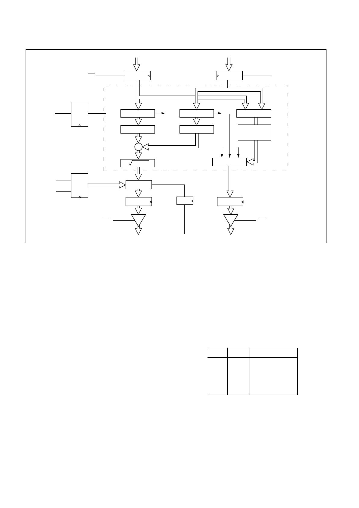
FUNCTIONAL DESCRIPTION
The PDSP16330 converts incoming Cartesian Data
into the equivalent Polar Values. The device accepts new 16
+ 16 bit complex data every cycle, and delivers a 16 bit + 12
bit Polar equivalent after 24 clock cycles.The input data can be
in 2s’ Complement or Sign Magnitude format selected via the
FORM input. The output is in a magnitude format for both the
Magnitude output and the Phase. Phase data is zero for data
with a zero Y input and positive X, and is 400 hex for zero X
data and positive Y, is 800 hex for zero Y data and negative X,
and is C00 hex for zero X and negative Y. The LSB weighting
(bit 0) is 2 x π/4096 radians. The 16 bit Magnitude result may
be scaled by shifting one, two, or three places in the more
significant direction, effectively multiplying the Magnitude
result by 2,4 or 8 respectively. Any of these shifts can under
certain conditions cause an invalid result to be output from the
device. Under these circumstances the OVR output will
become active. The PDSP16330 has independent clock
enables and three state output controls for all ports.
FORM
This input selects the format of the X and Y input data.
A low level on FORM indlcates that the Input data is twos’
complement format (Note: input data 8000 hex is not valid in
2s’ complement mode). This input refers to the format of the
current Input data and may be changed on a per cycle basis
if desired. The level of FORM is latched at the same time as
the data to which it refers.
S1-0
These inputs select the scaling factor to be applied to
the Magnitude output. They are latched by the rising edge of
CLK and determine the scaling of the output in the cycle after
they are loaded into the device. The scale factor applied is
determined by the table. Should the scaling factor applied
cause an invalid Magnitude result to be output on the M Port,
then the OVR Flag will become active for the period that the
M Port output is invalid.
The output number range is from 0 to 2 when the
scaling factor is set at x1.
S0
0
1
0
1
Scaling Factor
x1
x2
x4
x8
S1
0
0
1
1
Fig.2 Block diagram
+
SHIFT
16
32
30
15
16
16 16
9
9
12
2
OEM
S0
S1
FORM
CEX
SIGN
15
30
SIGN X SIGN Y
X > Y
OEP
P11:0OVRM15:0
X
2
MAGNITUDE MAGNITUDE
Y
2
X2 + Y
2
ROTATE
SIGN
Y/X
CEY
/4
ARCTAN
ROM
Y15:0X15:0
π
Page 3
PDSP16330/A/B
3
PIN DESCRIPTIONS
Symbol Pin Name and Description
CLK Clock: Common Clock to device Registers. Register contents change on the rising edge of clock.
Both pins must be connected.
CEX Clock Enable: Clock Enable for X Port. The clock to the X port is enabled by a low level.
CEY Clock Enable: Clock Enable for Y Port The clock to the Y port is enabled by a low level.
X15-X0 X Data Input Data presented to this input is loaded into the device by the rising edge of CLK.
X15 is the MSB
Y15-Y0 Y Data Input Data presented to this input is loaded into the device by the rising edge of CLK.
Y15 is the MSB
M15-M0 M Data Output: Magnitude data generated by the device is output on this port. Data changes on
the rising edge of CLK, M15 is the MSB. The weighting of M15 is determined by the Scale factor
selected .
P11-P0 P Data Output: Phase data generated by the device is output on this port. Data changes on the
rising edge of CLK, P11 is the MSB. The weighting of P11 is π radians.
OEM Output Enable: Output Enable for M Port. The M Port is in a high impedance state when this input
is high.
OEP Output Enable: Output Enable for P Port. The P Port is in a high impedance state when this input
is high.
FORM Format Select This input selects the format of the Cartesian Data input on the X and Y ports.
This input is latched by the rising edge of CLK, and is applied at the same time as the data to
which it refers. A low !evel indicates that two’s complement data is applied, a high indicates
Sign-Magnitude
S1-S0 Scaling Control: Control input for scaling of Magnitude Data. This input is latched by the rising
edge of CLK, and determines the scaling to be applied to the Magnitude result. The Scaling is
applied to the output data in the cycle following the cycle in which the control was latched.
OVR Overflow: Overflow flag. This signal becomes active if the scaling currently selected causes an
invalid value to be presented to the Magnitude output.
Vcc +5V supply. All Vcc pins must be connected.
GND 0V supply. All GND pins must be connected.
2's Complement
7FFF
.
.
.
0001
0000
FFFF
.
.
.
8001
Sign Magnitude
7FFF
.
.
.
0001
.
.
.
FFF
0000
8000
INPUT DATA RANGE
Page 4

PDSP16330/A/B
4
*
*
*
*
*
*
*
†
*
†
Sub-
group
1,2,3
1,2,3
1,2,3
1,2,3
1,2,3
1,2,3
1,2,3
1,2,3
ELECTRICAL CHARACTERISTICS
Test conditions (unless otherwise stated): T
amb
(Commercial) = 0°C to + 70°C, T
amb
(Industrial) = -40°C to + 85°C
V
cc
(Commercial) = 5.0V + 5%, Vcc (Industrial and Military) = 5.0V + 1%, GND = 0V
STATIC CHARACTERISTICS
Value
Characteristic Symbol Units Conditions
Min. Typ. Max.
Output high voltage V
OH
2.4 V IOH = 3.2mA
Output low voltage V
OL
0.6 V lOL=-3.2mA
Input high voltage (CMOS) V
IH
3.0 V Inputs CEX, CEY and CLK only
Input low voltage (CMOS) V
IL
1.0 V Inputs CEX, CEY and CLK only
Input high voltage (TTL) V
IH
2.2 V All other inputs
Input low voltage (TTL) V
IL
0.8 V All other inputs
Input leakage current (Note 1 ) I
IL
-10 + 120 µA GND < VIN<V
CC
Input capacitance C
IN
10 pF
Output leakage current l
oz
-50 + 50 µA GND <VIN < V
CC
Output SC current I
OS
-50 230 mA Vcc = Max
NOTES
1. All inputs except clock inputs have high value pull-down resistors
2. All parameters marked * are tested during production. Parameters marked † are guaranteed by design and characterisation.
Pin No.
AC
F3
G3
G1
G2
F1
H1
H2
J1
K1
J2
L1
K2
K3
L2
L3
K4
L4
J5
K5
L5
K6
J6
J7
L7
K7
L6
L8
K8
Function
M7
M6
M5
M4
M3
M2
M1
M0
S0
S1
GND
Vcc
FORM
Y15
Y14
Y13
Y12
Y11
Y10
Y9
Y8
Y7
Y6
Y5
Y4
Y3
Y2
Y1
Pin No.
AC
L9
L10
K9
L11
K10
J10
K11
J11
H10
H11
F10
G10
G11
G9
F9
F11
E11
E10
E9
D11
D10
C11
B11
C10
A11
B10
B9
A10
Function
YO
CEY
CLK
Vcc
GND
GND
GND
GND
GND
GND
GND
OEP
P0
P1
P2
P3
P4
P5
P6
P7
P8
P9
P10
P11
GND
Vcc
CEX
X0
Pin No.
AC
A9
B8
A8
B6
B7
A7
C7
C6
A6
A5
B5
C5
A4
B4
A3
A2
B3
A1
B2
C2
B1
C1
D2
D1
E3
E2
E1
F2
Function
X1
X2
X3
X4
X5
X6
X7
X8
X9
X10
X11
X12
X13
X14
X15
CLK
OVR
Vcc
GND
OEM
M15
M14
M13
M12
M11
M10
M9
M8
PIN FUNCTION
GC
91
92
93
94
95
96
97
98
99
100
1
6
7
8
9
10
11
12
13
14
15
16
17
18
19
20
21
22
GC
23
24
25
26
31
32
33
34
35
36
37
38
39
40
41
42
43
44
45
46
47
48
49
50
51
52
57
58
GC
59
60
61
62
63
64
65
66
67
68
69
70
71
72
73
74
75
76
81
82
83
84
85
86
87
88
89
90
Page 5

PDSP16330/A/B
5
Max.
25
24
PDSP16330A
Min.
12
2
12
0
12
2
5
50
15
15
24
Max.
25
24
25
25
25
25
180
120
Characteristic
† Input data setup to clock rising edge
† Input data Hold after clock rising edge
† CEX, CEY Setup to clock rising edge
† CEX, CEY Hold aher clock rising edge
† FORM, S1:0 Setup to clock rising edge
† FORM, S1:0 Hold after clock rising edge
† Clock rising edge to valid data
* Clock period
† Clock high time
† Clock low time
† Latency
† OEM, OEP low to data high data valid
† OEM, OEP low to data low data valid
† OEM, OEP high to data high impedance
† OEM, OEP low to data high impedance
† Vcc current (TTL input levels)
† Vcc current (CMOS input levels)
SWITCHING CHARACTERISTICS
NOTES
1. LSTTL is equivalent to IOH = 20µA, IOL = -0.4mA
2. Current is defined as negative into the device
3. CMOS input levels are defined as: VIH = VDD - 0.5V, VIL = +0.5V
4. All parameters marked * are tested during production.
Parameters marked † are guaranteed by design and characterisation.
5. All timings are dependent on silicon speed. This speed is tested by measuring clock period.
This guarantees all other timings by characterisation and design.
Value
PDSP16330
Min.
15
2
30
0
15
7
5
100
25
25
24
Max.
40
24
30
30
30
30
110
70
PDSP16330B
Min.
12
2
12
0
12
2
5
40
15
15
24
25
25
25
25
225
150
Units
ns
ns
ns
ns
ns
ns
ns
ns
ns
ns
cycles
ns
ns
ns
ns
mA
mA
Conditions
2 x LSTTL + 20pF
2 x LSTTL + 20pF
2 x LSTTL + 20pF
2 x LSTTL + 20pF
2 x LSTTL + 20pF
VCC = Max
Outputs unloaded
Clock freq. = Max
VCC = Max
Outputs unloaded
Clock freq. = Max
ABSOLUTE MAXIMUM RATINGS
Supply voltage, V
cc
-0.5V to + 7.0V
Input voltage, V
IN
-0.5V to VCC + 0.5V
Output voltage, V
our
-0.5V to VCC + 0.5V
Clamp diode current per pin, IK (see Note 2) ±18mA
Static discharge voltage (HMB), V
STAT
500V
Storage temperature. T
stg
-65°C to + 150°C
Ambient temperature with
power applied T
amb
:
Commercial 0°C to + 70°C
Industrial -40°C to + 85°C
Military -55 °C to + 125°C
Package power dissipation P
TOT
1200mW
Junction temperature 150°C
THERMAL CHARACTERISTICS
Package Type
θ
JC°C/W
θ
JA°C/W
AC 12 36
GC 12 35
NOTES
1. Exceeding these ratings may cause permanent damage.
Functional operatlon under these conditions is not implied.
2. Maximum dissipation or 1 second should not be exceeded;
only one output to be tested at any one time.
3. Exposure to Absoulte Maximum Ratings for extended periods
may affect device reliability.
Page 6

PDSP16330/A/B
6
0.5V
0.5V
0.5V
0.5V
V
H
V
L
1.5V
1.5V
Delay from ouput
low to output
high impedance
Delay from ouput
high impedance to
Output low
Delay from ouput
high to output
high impedance
Delay from ouput
high impedance to
Output high
NOTES
1. V
H
- Voltage reached when output driven high
2. V
L
- Voltage reached when output driven low
Test Waveform - measurement level
DUT
100p
I
OH
1.5V
I
OL
Fig.3 Three state delay measurement load
Page 7

Page 8

Page 9

M Mitel (design) and ST-BUS are registered trademarks of MITEL Corporation
Mitel Semiconductor is an ISO 9001 Registered Company
Copyright 1999 MITEL Corporation
All Rights Reserved
Printed in CANADA
TECHNICAL DOCUMENTATION - NOT FOR RESALE
World Headquarters - Canada
Tel: +1 (613) 592 2122
Fax: +1 (613) 592 6909
North America Asia/Pacific Europe, Middle East,
Tel: +1 (770) 486 0194 Tel: +65 333 6193 and Africa (EMEA)
Fax: +1 (770) 631 8213 Fax: +65 333 6192 Tel: +44 (0) 1793 518528
Fax: +44 (0) 1793 518581
http://www.mitelsemi.com
Information relating to products and services furnished herein by Mitel Corporation or its subsidiaries (collectively “Mitel”) is believed to be reliable. However, Mitel assumes no
liability for errors that may appear in this publication, or for liability otherwise arising from the application or use of any such information, product or service or for any infringement of
patents or other intellectual property rights owned by third parties which may result from such application or use. Neither the supply of such information or purchase of product or
service conveys any license, either express or implied, under patents or other intellectual property rights owned by Mitel or licensed from third parties by Mitel, whatsoever.
Purchasers of products are also hereby notified that the use of product in certain ways or in combination with Mitel, or non-Mitel furnished goods or services may infringe patents or
other intellectual property rights owned by Mitel.
This publication is issued to provide information only and (unless agreed by Mitel in writing) may not be used, applied or reproduced for any purpose nor form part of any order or
contract nor to be regarded as a representation relating to the products or services concerned. The products, their specifications, services and other information appearing in this
publication are subject to change by Mitel without notice. No warranty or guarantee express or implied is made regarding the capability, performance or suitability of any product or
service. Information concerning possible methods of use is provided as a guide only and does not constitute any guarantee that such methods of use will be satisfactory in a specific
piece of equipment. It is the user’s responsibility to fully determine the performance and suitability of any equipment using such information and to ensure that any publication or
data used is up to date and has not been superseded. Manufacturing does not necessarily include testing of all functions or parameters. These products are not suitable for use in
any medical products whose failure to perform may result in significant injury or death to the user. All products and materials are sold and services provided subject to Mitel’s
conditions of sale which are available on request.
 Loading...