MITEL PDSP16318A, PDSP16318GC1R, PDSP16318IG, PDSP16318MC Datasheet

PDSP16318/PDSP16318A
PDSP16318/16318A
Complex Accumulator
Advance Information
Supersedes version DS3708 - 2.4 September 1996 DS3708 - 3.1 November 1998
The PDSP16318/A contains two independent 20-bit
Adder/Subtractors combined with accumulator registers and
shift structures. The four port architecture permits full 20MHz
throughout in FFT and filter applications.
Two PDSP16318As combined with a single PDSP16112A
Complex Multiplier provide a complete arithmetic solution for
a Radix 2 DIT FFT Butterfly. A new complex Butterfly result
can be generated every 50ns allowing 1K complex FFTs to be
executed in 256µs.
FEATURES
GC100
■ Full 20MHz Throughout in FFT Applications
■ Four Independent 16-bit I/O Ports
■ 20-bit Addition or Accumulation
■ Fully Compatible with PDSP16112 Complex Multiplier
■ On Chip Shift Structures for Result Scaling
■ Overflow Detection
■ Independent Three-State Outputs and Clock
Enables for 2 Port 20MHz Operation
■ 1.4 micron CMOS
■ 500mW Maximum Power Dissipation
■ 100 CQFP package
APPLICATIONS
■ High speed Complex FFT or DFTs
■ Complex Finite Impulse Response (FIR) Filtering
■ Complex Conjugation
■ Complex Correlation/Convolution
A
REG DELAY
Fig.1 Pin connections - Top view (GC100)
ASSOCIATED PRODUCTS
PDSP16112 16 x 12 Complex Multiplier
PDSP16116 16 x 16 Complex Multiplier
PDSP1601 ALU and Barrel Shifter
PDSP16330 Pythagoras Processor
ORDERING INFORMATION
Industrial (-40°C to +85°C)
PDSP16318A/IG/GC1R (20MHz - QFP)
Military (-55°C to +125°C)
PDSP16318/MC/GC1R (10MHz - QFP
MIL STD 883C Screened)
N.B. Further details of the Military grade part are available
in a separate datasheet
B
SHIFT
REG
C
A
A
SHIFT
B
REG
B
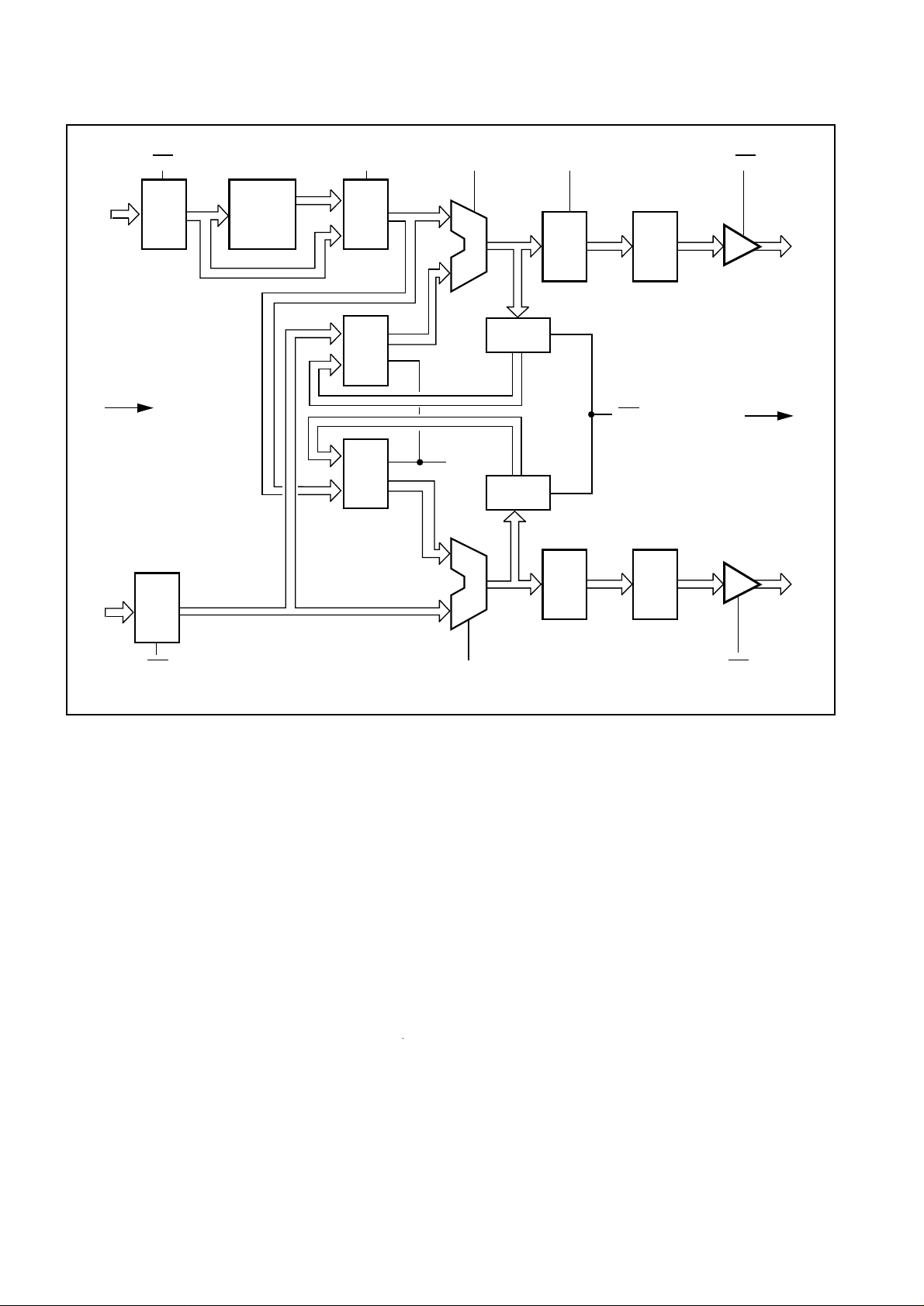
Fig. 2 PDSP16318 simplified block diagram
REG
D
1

PDSP16318/16318A
16 16
A
CLK
B
A REG
REG
S2:0ASRDELCEA
8
CYCLE
DELAY
1616
MUX
MUX
MUX
20
B
20 16 16
SHIFT
A
20
20
20
MS
20
A
B
REG
REG
20
SHIFT
REG
CLR OVR
REG
OEC
D
1616
D
CEB ASI OED
Fig. 3 Block diagram
2

FUNCTIONAL DESCRIPTION
The PDSP16318 is a Dual 20-bit Adder/Subtractor
configured to support Complex Arithmetic. The device may be
used with each of the adders allocated to real or imaginary
data (e.g. Complex Conjugation), the entire device allocated
to Real or Imaginary Data (e.g. Radix 2 Butterflys) or each of
the adders configured as accumulators and allocated to real
or imaginary data (Complex Filters). Each of these modes
ensures that a full 20MHz throughput is maintained through
both adders, the first and last mode illustrating true Complex
operation, where both real and imaginary data is handled by
the single device.
Both Adder/Subtractors may be controlled
independently via the ASR and ASI inputs. These controls
permit A + B, A - B, B - A or pass A operations, where the A
input to the Adder is derived from the input multiplexer. The
CLR control line allows the clearing of both accumulator
registers. The two multiplexers may be controlled via the MS
inputs, to select either new input data, or fed-back data from
PDSP16318/16318A
the accumulator registers. The PDSP16318 contains an 8cycle deskew register selected via the DEL control. This
deskew register is used in FFT applications to ensure correct
phasing of data that has not passed through the PDSP16112
Complex Multiplier.
The 16-bit outputs from the PDSP16318 are derived from
the 20-bit result generated by the Adders. The three bit S2:0
input selects eight different shifted output formats ranging
from the most significant 16 bits of the 20-bit data, to the least
significant 13 bits of the 20-bit data. In this mode the 14th, 15th
and 16th bits of the output are set to zero. The shift selected
is applied to both adder outputs, and determines the function
of the OVR flag. The OVR flag becomes active when either of
the two adders produces a result that has more significant
digits than the MSB of the 16-bit output from the device. In this
manner all cases when invalid data appears on the output are
flagged.
Symbol
A15:0
B15:0
C15:0
D15:0
CLK
CEA
CEB
OEC
OED
OVR
ASR1:0
ASI1:0
CLR
MS
S2:0
Type
Input
Input
Output
Output
Input
Input
Input
Input
Input
Output
Input
Input
Input
Input
Input
Description
Data presented to this input is loaded into the input register on the rising edge of CLK. A15 is the MSB.
Data presented to this input is loaded into the input register on the rising edge of CLK. B15 is the MSB
and has the same weighting as A15.
New data appears on this output after the rising edge of CLK. C15 is the MSB.
New data appears on this output after the rising edge of CLK. C15 is the MSB.
Common Clock to all internal registers
Clock enable: when low the clock to the A input register is enabled.
Clock enable: when low the clock to the B input register is enabled.
Output enable: Asynchronous 3-state output control: The C outputs are in a high impedance
state when this input is high.
Output enable: Asynchronous 3-state output control: The D outputs are in a high impedance
state when this input is high.
Overflow flag: This flag will go high in any cycle during which either the output data overflows the number
range selected or either of the adder results overflow. A new OVR appears after the rising edge of the
CLK.
Add/subtract Real: Control input for the 'Real' adder. This input is latched by the rising edge of clock.
Add/subtract Imag: Control input for the 'Imag' adder. This input is latched by the rising edge of clock.
Accumulator Clear: Common accumulator clear for both Adder/Subtractor units. This input is latched by
the rising edge of CLK.
Mux select: Control input for both adder multiplexers. This input is latched by the rising edge of CLK.
When high the feedback path is selected.
Scaling control: This input selects the 16-bit field from the 20-bit adder result that is routed to the outputs.
This input is latched by the rising edge of CLK.
DEL
VCC
GND
Input
Power
Ground
Delay Control: This input selects the delayed input to the real adder for operations involving the
PDSP16112. This input is latched by the rising edge of CLK.
+5V supply: Both Vcc pins must be connected.
0V supply: Both GND pins must be connected.
3
 Loading...