MITEL PDSP16116, PDSP16116A, PDSP16116MC Datasheet
PDSP16116/A/MC
PDSP16116/A/MC
16 By 16 Bit Complex Multiplier
Supersedes July 1993 version, DS3858 - 1.0 DS3858 - 2.0 October 1998
The PDSP16116A will multiply two complex (16 + 16) bit
words every 50ns and can be configured to output the
complete complex (32 + 32) bit result within a single cycle. The
data format is fractional two's complement.
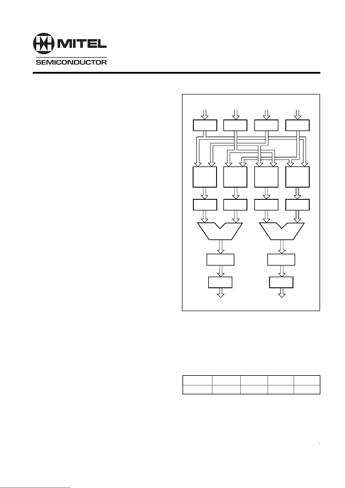
The PDSP16116/A contains four 16 x 16 Array Multipliers,
two 32 bit Adder/Subtractors and all the control logic required
to support Block Floating Point Arithmetic as used in FFT
applications. In combination with a PDSP16318, the
PDSP16116A forms a two chip 10MHz Complex Multiplier
Accumulator with 20 bit accumulator registers and output
shifters. The PDSP16116 in combination with two
PDSP16318s and two PDSP1601s forms a complete 10MHz
Radix 2 DIT FFT Butterfly solution which fully supports Block
Floating Point Arithmetic. The PDSP16116/A has an
extremely high throughput that is suited to recursive
algorithms as all calculations are performed with a single
pipeline delay (two cycle fall-through).
FEATURES
XR XI YR YI
REG REG REG REG
MULTMULTMULTMULT
REG REG REG
REG
■ Complex Number (16 + 16) X (16 + 16) Multiplication
■ Full 32 bit Result
■ 20MHz Clock Rate
■ Block Floating Point FFT Butterfly Support
■ -1 times -1 Trap
■ Two's Complement Fractional Arithmetic
■ TTL Compatible I/O
■ Complex Conjugation
■ 2 Cycle Fall Through
■ 144 pin PGA or QFP packages
APPLICATION
■ Fast Fourier Transforms
■ Digital Filtering
■ Radar and Sonar Processing
■ Instrumentation
■ Image Processing
ASSOCIATED PRODUCTS
PDSP16318/A Complex Accumulator
PDSP16112/A (16 + 16) X (12 + 12) Complex Multiplier
PDSP16330/A Pythagoras Processor
PDSP1601/A ALU and Barrel Shifter
PDSP16350 Precision Digital Modulator
PDSP16256 Programmable FIR Filter
PDSP16510 Single Chip FFT Processor
+/- +/-
SHIFT
REG
PR PI
Fig.1 Simplified Block Diagram
CHANGE NOTIFICATION
The change notification requirements of MIL-M-38510 will be
implemented on this device type. Known customers will be
notified of any changes since last buy when ordering further
parts if significant changes have been made.
Rev A B C D
Date JULY 1993 OCT 1998
SHIFT
REG
1
PDSP16116/A/MC
The PDSP16116 has a number of features tailored for
System applications.
-1 x -1 Trap
In multiply operations utilising Twos Complement
Fractional notation, the -1 x -1 operation forms an invalid result
as +1 is not representable in the fractional number range. The
PDSP16116/A eliminates this problem by trapping the
-1 x -1 operation and forcing the Multiplier result to become the
most positive representable number.
Complex Conjugation
Many algorithms utilising complex arithmetic require
conjugation of complex data stream. This operation has
Signal
Type
Description
traditionally required an adiditional ALU to multiply the
imaginary component by -1. The PDSP16116 eliminates the
requirement for the extra ALU by offering on chip complex
conjugation of either of the two incoming complex data words
with no loss in throughput.
Easy Interfacing
As with all PDSP family members the PDSP16116 has
registered I/O for data and control. Data inputs have
independent clock enables and data outputs have
independent three state output enables.
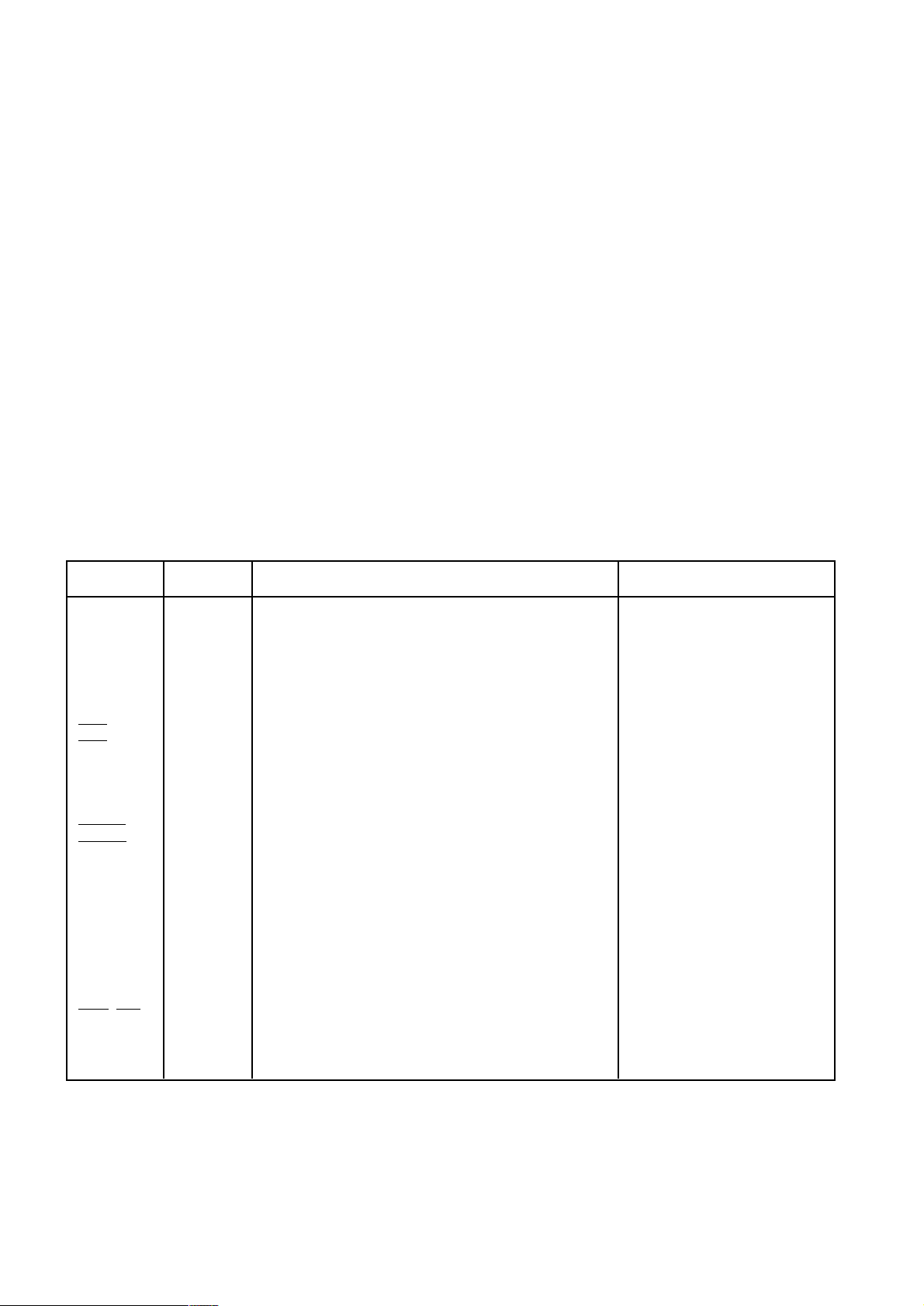
Normal mode Configuration
XR15:0
XI15:0
YR15:0
YI15:0
PR15:0
PI15:0
CLK
CEX
CEY
CONX
CONY
ROUND
MBFP
SOBFP
EOPSS
AR15:13
AI15:13
WTA1:0
WTB1:0
WTOUT1:0
SFTA1:0
SFTR2:0
GWR4:0
OSEL1:0
OER, OEI
VDD
GND
INPUT
INPUT
INPUT
INPUT
OUTPUT
OUTPUT
INPUT
INPUT
INPUT
INPUT
INPUT
INPUT
INPUT
INPUT
INPUT
INPUT
INPUT
INPUT
INPUT
OUTPUT
OUTPUT
OUTPUT
OUTPUT
INPUT
INPUT
POWER
POWER
16 bit input for real x data
16 bit input for imag x data
16 bit input for reaal y data
16 bit input for imag y data
16 bit output for real p data
16 bit output for img p data
Clock, new data is loaded on rising edge of CLK
Clock, enable X-port input register
Clock, enable Y-port input register
Conjugate X data
Conjugate Y data
Rounds the real & imag results
Mode select (BFP/Normal)
Start of BFP operations **
End of pass **
3 MSB's from real part of A-word **
3 MSB's from imag part of A-word **
Word tag from A-word
Word tag from B-word / shift control *
Word tag output **
Shift control for A-word / overflow flag *
Shift control for accumulator resul **
Global weighting register contents **
Selects the desired output configuration
Output enables
+5V Supply All supply pins
0V Supply must be connected
Tie Low
Tie Low
Tie Low
Tie Low
Tie Low
Tie Low
* Indicates pin performs different functions in BFP / Normal modes.
** Indicates pin is used only in BFP mode
Table.1 Signal Descriptions
2
CEX
PDSP16116/A/MC
XR XI YR YI
CEY
REG REG REG REG
'1'
ROUND
WTA
AR15:13
WTB
AI15:13
SOBFP
EOPSS
SFTR
SFTA
GWR4:0
WTOUT
C
O
M
P
OVR
CONTROL
16X16
MULT
MUX MUX MUX MUX
REG REG REG REG
C
O
M
P
16X16
MULT
C
O
M
P
16X16
MULT
C
O
M
P
ADD/SUB ADD/SUB
CONX CONY
SHIFT SHIFT
LOGIC
REG
DECODE
REG
16X16
MULT
MUX
OSEL
MUX
OEIOER
PIPR
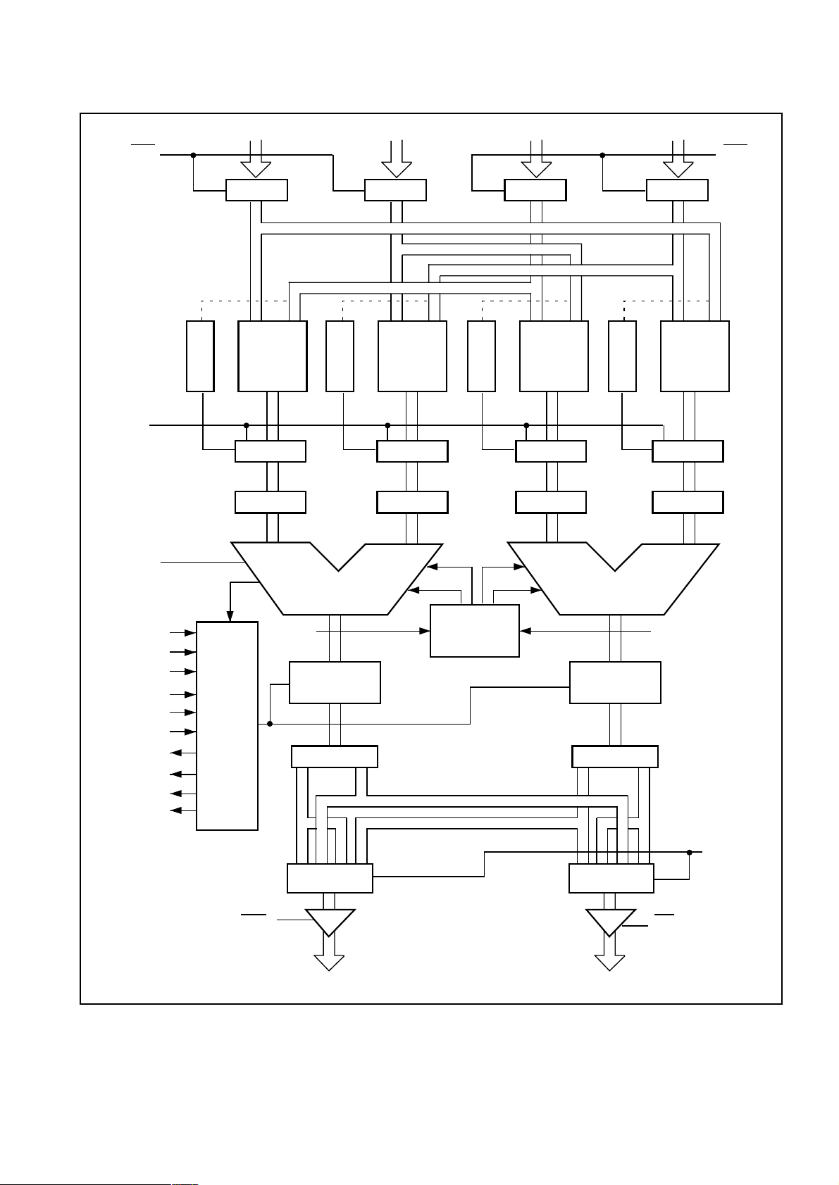
Fig.2 Block Diagram
3

PDSP16116/A/MC
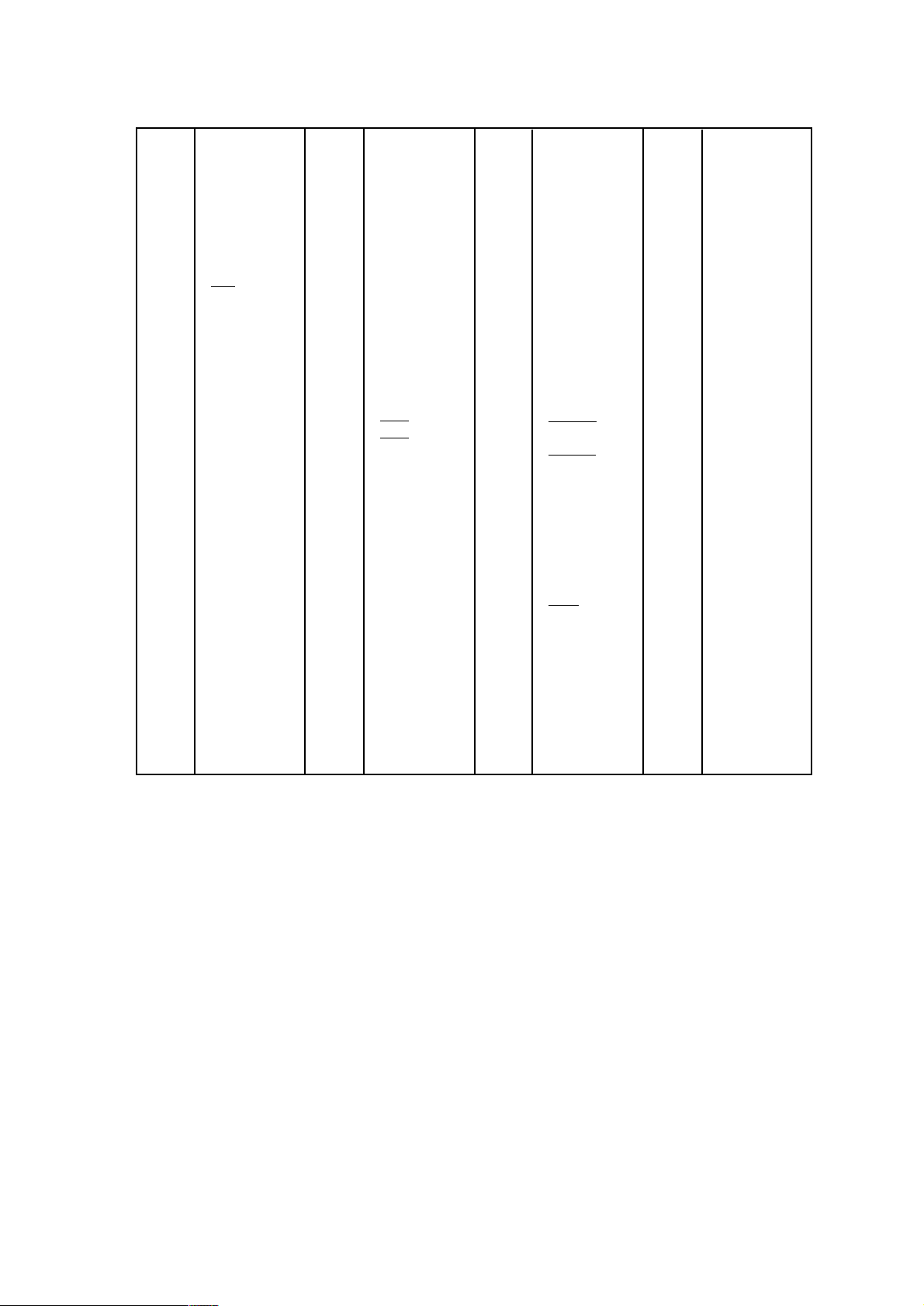
Fig.3 Pin Allocation Diagram (Bottom View)
144 pin PGA - AC144
4
PDSP16116/A/MC
GG
1
2
3
4
5
6
7
8
9
10
11
12
13
14
15
16
17
18
19
20
21
22
23
24
25
26
27
28
29
30
31
32
33
34
35
36
SIG
PI14
PI15
WTOUT1
WTOUT0
SFTR0
SFTR1
SFTR2
OEI
CONX
CONY
ROUND
AI13
AI14
AI15
AR13
AR14
AR15
YI15
YI14
YI13
YI12
YI11
YI10
YI9
YI8
YI7
YI6
YI5
YI4
YI3
YI2
YI1
YI0
XI0
GND
VDD
GG
37
38
39
40
41
42
43
44
45
46
47
48
49
50
51
52
53
54
55
56
57
58
59
60
61
62
63
64
65
66
67
68
69
70
71
72
SIG
XI1
XI2
XI3
XI4
XI5
XI6
XI7
XI8
XI9
XI10
XI11
XI12
XI13
XI14
XI15
CEY
CEX
XR15
XR14
XR13
XR12
XR11
XR10
XR9
XR8
XR7
XR6
XR5
XR4
XR3
XR2
XR1
XR0
YR15
YR14
YR13
GG
73
74
75
76
77
78
79
80
81
82
83
84
85
86
87
88
89
90
91
92
93
94
95
96
97
98
99
100
101
102
103
104
105
106
107
108
SIG
GND
VDD
YR12
YR11
YR10
YR9
YR8
YR7
YR6
YR5
YR4
YR3
YR2
YR1
YR0
EOPSS
VDD
SOBFP
WTB1
WTB0
WTA1
WTA0
MBFP
CLK
OSEL1
OSEL0
OER
SFTA0
SFTA1
GWR0
GWR1
GWR2
GWR3
GWR4
PR15
PR14
GG
109
110
111
112
113
114
115
116
117
118
119
120
121
122
123
124
125
126
127
128
129
130
131
132
133
134
135
136
137
138
139
140
141
142
143
144
SIG
GND
VDD
PR13
PR12
PR11
PR10
PR9
PR8
PR7
PR6
PR5
GND
VDD
PR4
PR3
PR2
PR1
PR0
PI0
PI1
PI2
PI3
PI4
VDD
PI5
GND
PI6
PI7
PI8
PI9
PI10
PI11
PI12
PI13
GND
VDD
All GND and VDD pins must be used.
Fig.3A Pin Allocation Diagram - 144 pin ceramic QFP - GC144
5
PDSP16116/A/MC
NORMAL MODE OPERATION
When the MBFP mode select input is held low the ‘Normal’
mode of operation is selected. This mode supports all
Complex Multiply operations that do not require Block Floating
Point arithmetic.
Multiplier Satge
Complex two's complement fractional data is loaded into
the X and Y input registers via the X and Y Ports on the rising
edge of CLK. The Real and Imaginary components of the
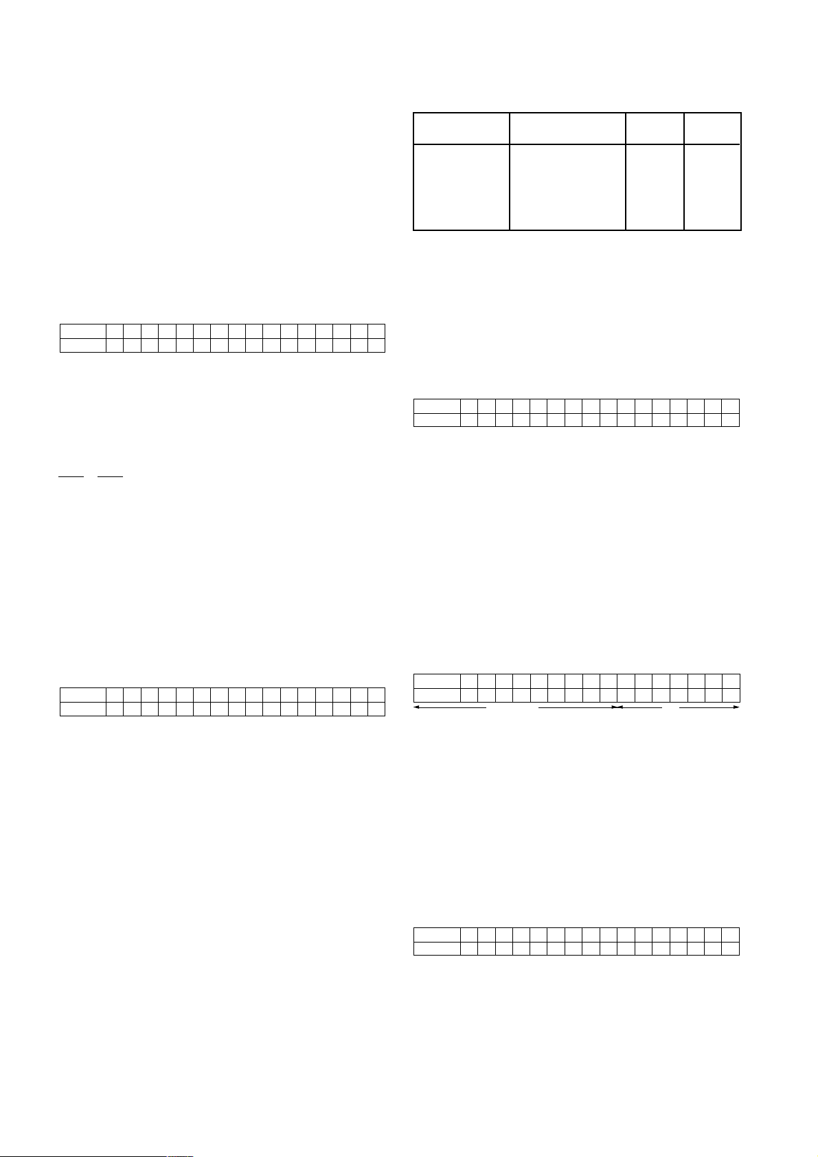
fractional data are each assumed to have the following format
BIT NUMBER 15 14 13 12 11 10 9 8 7 6 5 4 3 2 1 0
WEIGHTING S 2
Where S = sign bit which has an effective weighting -2
The value of the 16 bit two’s complement word is
Value = (-1xS)+(bit14x2-1)+(bit13x2-2)+(bit12x2-3). . .
The X & Y port registers are individually enabled by the
CEX & CEY signals respectvely. If the registers are required
to be permanently enabled, then these signals may be tied to
ground. On each clock cycle the contents of the input registers
are passed to the four multipliers to start a new Complex
Multiply operation. Each Complex Multiply operation requires
four partial products (Xr x Yr), (Xr x Yi), (Xi x Yr), (Xi x Yi), all
of which are calculated in parallel by the four 16 x 16
Multipliers. Only one clock cycle is required to complete the
multiply stage before the Mutliplier results are loaded into the
Multiplier output registers for passing on to the Adder/
Subtractors in the next cycle. Each multiplier produces a 31
bit result with the duplicate sign bit eliminated. The format of
the output data from the Multipliers is
BIT NUMBER 30 29 28 27 26 25 24 . . . 7 6 5 4 3 2 1 0
WEIGHTING S 2
-12-22-32-42-52-62-72-82-92-102-112-122-132-142-15
0
-12-22-32-42-52-6
-232-242-252-262-272-282-292-30
. . . 2
FUNCTION
X x Y
X x Conj Y
Conj X x Y
Invalid
OPERATION
(XR+XI)x(YR+YI)
(XR+XI)x(YR-YI)
(XR-XI)x(YR+YI)
Invalid
CONX
low
low
high
high
CONY
low
high
low
high
Table 3 Conjugate Functions
Adder / Subtractor Stage
The 31 bit Real and Imaginary results from the Multipliers
are passed to two 32 bit Adder/Subtractors. The Adder
calculates the imaginary result ((Xr x Yi) + (Xi x Yr)) and the
Subtractor calculates the Real result ((Xr x Yr) = (Xi x Yi)).
Each Adder/Subtractor produces a 32 bit result with the
following format.
BIT NUMBER 31 30 29 28 27 26 . . . 8 7 6 5 4 3 2 1 0
WEIGHTING S 2
The effective weighting of the sign bit is -2
02-12-22-32-4
-222-232-242-252-262-272-282-292-30
. . . 2
1
Rounding
The ROUND control when asserted rounds the most
significant 16 bits of the full 32 bit result from the Adder/
Subtractor. If the ROUND signal is active (High), then bit 16
is set to a one, rounding the most significant 16 bits of the
Adder/Subractor result. (The least siginificant 16 bits are
unaffected). Inserting a one ensures that the rounding error
is never greater than 1LSB, and that no DC bias is introduced
as a result of the rounding processes.
The format of the Rounded result is;
BIT NUMBER 31 30 29 28 27 . . . 18 17 16 15 14 13 . . . 2 1 0
WEIGHTING S 2
02-12-22-3
-122-132-142-152162-17
. . . 2
-282-292-30
. . . 2
LBS'sROUNDED VALUE
The effective weighting of the sign bit is -2
0
Result Correction
Due to the nature of the fraction twos complement
representation it is possible to represent -1 exactly but not 1.
With conventional multipliers this causes a problem when -1
is multiplied by -1 as the multiplier produces an incorrect
result. The PDSP16116 includes a trap to ensure that the
most positive number (value = 1.2
-30
), (hex = 7FFFFFFFF) is
subsituted for the incorrect result. The multiplier result is
therefore always a (correct) fractional value.
Complex Conjugation
Either the X or Y input data may be complex conjugated by
asserting the CONX or CONY signals respectively. Asserting
either of these signals has the effect of inverting (multiplying
by -1) the imaginary component of the respective input. Table
3 shows the effect of CONX and CONY on the X and Y inputs.
6
The effective weighting of the sign is -2
1
Shifter
Each of the two Adder/Subtractors are followed by Shifters
controlled via the WTB control input. These shifters can each
apply four different shifts, however the same shift is applied to
both real and imaginary components. The four shift options
are:
i) WTB1:0 = 11 Shift complex product one place to the left
giving a shifter output format:
BIT NUMBER 31 30 29 28 27 26 25 . . . 7 6 5 4 3 2 1 0
WEIGHTING S 2
The effective weighting of the sign bit is -2
-12-22-32-42-52-6
-242-252-262-272-282-292-302-31
. . . 2
0
 Loading...